si8931/32 data sheet
TRANSCRIPT

Si8931/32 Data Sheet
Isolated Amplifier for Voltage MeasurementThe Si8931/32 is a galvanically isolated analog amplifier optimized for voltage sensing. Its 2.5V input range is ideal for isolated voltage sensing applications. The output is a differentialanalog signal (Si8931) or single-ended signal (Si8932) that is proportional to the input voltage.
The Si8931/32 provides excellent linearity with low offset and gain drift to ensure that accuracyis maintained over the entire operating temperature range. Exceptionally high common-modetransient immunity means that the Si8931/32 delivers accurate measurements even in thepresence of high-power switching as is found in motor drive systems and inverters.
The Si8931/32 isolated voltage sensing amplifier utilizes Skyworks’ proprietary isolation tech-nology. It supports up to 5.0 kVrms withstand voltage per UL1577. This technology enableshigher performance, reduced variation with temperature and age, tighter part-to-part matching,and longer lifetimes compared to other isolation technologies.
Applications:• Industrial, HEV and renewable energy inverters• AC, Brushless, and DC motor controls and drives• Variable speed motor control in consumer white goods• Isolated switch mode and UPS power supplies• General industrial data acquisition and sensor interface• Automotive onboard chargers, battery management systems, and charging stations
Safety Approvals (pending):• UL 1577 recognized
• Up to 5000 Vrms for 1 minute• CSA approval
• IEC 60950-1, 62368-1 (reinforced insulation)• VDE certification conformity
• VDE0884 Part 11 (basic/reinforced insulation)• CQC certification approval
• GB4943.1-2011
KEY FEATURES
• 0 to 2.5 V nominal input voltage• Low signal delay: 1 µs• Typical input offset: 0.16 mV• Typical gain error: ±0.06%• Excellent drift specifications
• 0.75 µV/°C offset drift• 6 ppm/°C typical gain drift
• Typical nonlinearity: 0.01%• Typical SNR: 76 dB• High common-mode transient
immunity: 75 kV/µs• Auomotive-grade OPNs
• AIAG-compliant PPAPdocumentation support
• IMDS and CAMDS listingsupport
• Compact packages• 8-pin wide body stretched SOIC• 8-pin narrow body SOIC
• –40 to 125 °C
OSC
PWMVIN
ReceiverNC
Transmitter
AOP
AONPWM
VDDB
GNDB
VDDA
GNDA
Si8931
CM
OS
Isol
atio
n
OSC
PWMVIN
ReceiverNC
Transmitter
PWM
VDDB
GNDB
VDDA
GNDA
AO
GNDB
Si8932
CM
OS
Isol
atio
n
Skyworks Solutions, Inc. • Phone [781] 376-3000 • Fax [781] 376-3100 • [email protected] • www.skyworksinc.com1 Rev. 0.8 • Skyworks Proprietary Information • Products and Product Information are Subject to Change Without Notice • December 4, 2021 1

1. Ordering Guide
Ordering PartNumber1, 2, 3
AutomotiveOrdering PartNumber1, 2, 3, 4
Ordering Options
Input Range Isolation Rating Output Package Type
Si8931D-IS4 Si8931D-AS4 0 to 2.5 V nominal 5.0 kVrms Differential WB StretchedSOIC-8
Si8931B-IS Si8931B-AS 0 to 2.5 V nominal 2.5 kVrms Differential NB SOIC-8
Si8932D-IS4 Si8932D-AS4 0 to 2.5 V nominal 5.0 kVrms Single-ended WB StretchedSOIC-8
Si8932B-IS Si8932B-AS 0 to 2.5 V nominal 2.5 kVrms Single-ended NB SOIC-8
Note:1. All packages are RoHS-compliant.2. “Si” and “SI” are used interchangeably.3. AEC-Q100 pending qualification.4. Automotive-Grade devices ("-A" suffix) are identical in construction materials, topside marking, and electrical parameters to their
Industrial Grade ("-I suffix") version counterparts. Automotive-Grade products are produced utilizing full automotive process flowsand additional statistical process controls throughout the manufacturing flow. The Automotive-Grade part number is included onshipping labels.
Si8931/32 Data Sheet • Ordering Guide
Skyworks Solutions, Inc. • Phone [781] 376-3000 • Fax [781] 376-3100 • [email protected] • www.skyworksinc.com2 Rev. 0.8 • Skyworks Proprietary Information • Products and Product Information are Subject to Change Without Notice • December 4, 2021 2

Table of Contents1. Ordering Guide . . . . . . . . . . . . . . . . . . . . . . . . . . . . . . 2
2. System Overview . . . . . . . . . . . . . . . . . . . . . . . . . . . . . . 42.1 Fail-Safe and Low-Power Modes . . . . . . . . . . . . . . . . . . . . . . . . 5
3. Voltage Sense Application . . . . . . . . . . . . . . . . . . . . . . . . . . 6
4. Electrical Specifications . . . . . . . . . . . . . . . . . . . . . . . . . . . 74.1 Regulatory Information . . . . . . . . . . . . . . . . . . . . . . . . . . .12
4.2 Typical Operating Characteristics . . . . . . . . . . . . . . . . . . . . . . . .14
5. Pin Descriptions . . . . . . . . . . . . . . . . . . . . . . . . . . . . . 195.1 Si8931 Pin Descriptions . . . . . . . . . . . . . . . . . . . . . . . . . . .19
5.2 Si8932 Pin Descriptions . . . . . . . . . . . . . . . . . . . . . . . . . . .20
6. Packaging . . . . . . . . . . . . . . . . . . . . . . . . . . . . . . . 216.1 Package Outline: 8-Pin Wide Body Stretched SOIC . . . . . . . . . . . . . . . . .21
6.2 Package Outline: 8-Pin Narrow Body SOIC . . . . . . . . . . . . . . . . . . . .23
6.3 Land Pattern: 8-Pin Wide Body Stretched SOIC . . . . . . . . . . . . . . . . . . .25
6.4 Land Pattern: 8-Pin Narrow Body SOIC . . . . . . . . . . . . . . . . . . . . .26
6.5 Top Marking: 8-Pin Wide Body Stretched SOIC . . . . . . . . . . . . . . . . . . .27
6.6 Top Marking: 8-Pin Narrow Body SOIC . . . . . . . . . . . . . . . . . . . . . .28
7. Revision History . . . . . . . . . . . . . . . . . . . . . . . . . . . . . 29
Skyworks Solutions, Inc. • Phone [781] 376-3000 • Fax [781] 376-3100 • [email protected] • www.skyworksinc.com3 Rev. 0.8 • Skyworks Proprietary Information • Products and Product Information are Subject to Change Without Notice • December 4, 2021 3
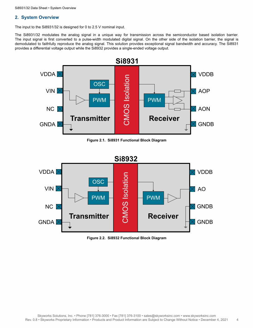
2. System Overview
The input to the Si8931/32 is designed for 0 to 2.5 V nominal input.
The Si8931/32 modulates the analog signal in a unique way for transmission across the semiconductor based isolation barrier.The input signal is first converted to a pulse-width modulated digital signal. On the other side of the isolation barrier, the signal isdemodulated to faithfully reproduce the analog signal. This solution provides exceptional signal bandwidth and accuracy. The Si8931provides a differential voltage output while the Si8932 provides a single-ended voltage output.
OSC
PWMVIN
ReceiverNC
Transmitter
AOP
AONPWM
VDDB
GNDB
VDDA
GNDA
Si8931
CM
OS
Isol
atio
n
Figure 2.1. Si8931 Functional Block Diagram
OSC
PWMVIN
ReceiverNC
Transmitter
PWM
VDDB
GNDB
VDDA
GNDA
AO
GNDB
Si8932
CM
OS
Isol
atio
n
Figure 2.2. Si8932 Functional Block Diagram
Si8931/32 Data Sheet • System Overview
Skyworks Solutions, Inc. • Phone [781] 376-3000 • Fax [781] 376-3100 • [email protected] • www.skyworksinc.com4 Rev. 0.8 • Skyworks Proprietary Information • Products and Product Information are Subject to Change Without Notice • December 4, 2021 4

2.1 Fail-Safe and Low-Power Modes
The Si8931/32 implements a fail-safe output when the high-side supply voltage VDDA goes away. This is important for safe operationin systems with high safety requirements. The fail-safe output is nominally 2.8 V (Si8932) or –2.8 V (Si8931) which can be differentiatedfrom the maximum clipping output voltage of 2.6 V to simplify diagnostics on the system level.
Device Output Voltage(VDDA Normal)
Output Voltage(VDDA Removed)
Si8931 ~ ±2.6 V ~ –2.8 V
Si8932 0 to ~2.6 V ~ +2.8 V
In addition to the fail-safe output, when a loss of VDDA supply occurs, the part will automatically move into a lower power mode thatreduces IDDB current to approximately 1 mA. The controller side continues to monitor high-side communications to determine whenVDDA supply returns. When the supply voltage is returned, normal operation begins in approximately 250 μs. Similarly, a loss of VDDBsupply will reduce IDDA current to approximately 1 mA.
Si8931/32 Data Sheet • System Overview
Skyworks Solutions, Inc. • Phone [781] 376-3000 • Fax [781] 376-3100 • [email protected] • www.skyworksinc.com5 Rev. 0.8 • Skyworks Proprietary Information • Products and Product Information are Subject to Change Without Notice • December 4, 2021 5

3. Voltage Sense Application
A typical isolated voltage sensing application circuit is shown below. In this example, a high voltage is divided down to produce avoltage (VIN) within the optimum input signal range of the Si8931/32. Numerous alternative inputs configurations are possible withthe flexibility of a high impedance input isolator. The Si8931 senses the single-ended input voltage and reproduces it as a differential(or single-ended with the Si8932) output voltage across the galvanic isolation barrier. The Si8931 differential outputs (AOP, AON) canbe routed directly to a differential ADC as shown below. The Si8932 senses the single-ended input voltage and reproduces it as asingle-ended output voltage across the galvanic isolation barrier. The single-ended output can be routed directly to a standard ADC (notshown). If the voltage sensed is > 2.5 V, a simple voltage divider consisting of R1 and R2 can be used to scale down any voltage to fitthe input range of the Si8931/32. R2 < 10 kΩ is recommended for best performance.
C2
0.1µF
Si8931
VDDA
VIN
GNDA GNDB
VDDB
NC
1
2
3
4
3 to 5.5V Supply
3 to 5.5V Supply
C4
0.1µF
AOP7
5
8
6C6
R5
R6ADC
+
-
AON To ControllerC1
Vsource
R2 ≤ 10KΩ
R1
Figure 3.1. Voltage Sense Application
The amplifier bandwidth of the Si8931/32 is approximately 600 kHz. For applications where input filtering is required, a passive,differential RC low-pass filter can be placed at the input pin. Consider the source resistance of the signal measured (or the parallelcombination of R1 and R2 if using a voltage divider) as it should be included in the filter calculation. Capacitor C1 should be sized tomake a band limiting filter at the desired frequency.
C4, the local bypass capacitor for the B-side of Si8931/32, should be placed closed to VDDB supply pin with its return close to GNDB.The output signal at AOP and AON is differential with unity gain and common mode of 1.4 V. The outputs are sampled by a differentialinput ADC. Depending on the sample rate of the ADC, an anti-aliasing filter may be required. A simple anti-aliasing filter can bemade from the passive components, R5, C6, and R6. The characteristics of this filter are dictated by the input topology and samplingfrequency of the ADC. However, to ensure the Si8931/32 outputs are not overloaded, R5 = R6 > 5 kΩ and C6 can be calculated by thefollowing equation:
C6 = 12 × π × R5 + R6 × f3dB
Si8931/32 Data Sheet • Voltage Sense Application
Skyworks Solutions, Inc. • Phone [781] 376-3000 • Fax [781] 376-3100 • [email protected] • www.skyworksinc.com6 Rev. 0.8 • Skyworks Proprietary Information • Products and Product Information are Subject to Change Without Notice • December 4, 2021 6

4. Electrical Specifications
Table 4.1. Electrical Specifications
TA = –40 to +125 °C; typical specs at 25 °C with VDDA = VDDB = 5 V unless specified differently under Test Condition
Parameter Symbol Test Condition Min Typ Max Units
Input Side Supply Voltage VDDA 3.0 5.5 V
Input SupplyCurrent Si8931/32 IDDA VDDA = 3.3 V 3.8 4.7 5.7 mA
Output Side Supply Voltage VDDB 3.0 5.5 V
Output SupplyCurrent
Si8931 IDDB VDDB = 3.3 V 2.8 3.5 4.5 mA
Si8932 IDDB VDDB = 3.3 V 3 4.3 5 mA
Amplifier Bandwidth 600 kHz
Amplifier Input
Specified LinearInput Range VIN 0.25 2.25 V
Maximum Input Voltagebefore Clipping VIN 2.5 V
Input Referred Offset VOSTA = 25 °C,
VIN = 0.25 V–1 ±0.16 1 mV
Input Offset Drift VOST –25 ±0.75 25 µV/°C
Input Impedance RIN 500 MΩ
Amplifier Output
Full-scale Output 2.5 Vpk
Gain 1
Gain Error TA = 25 °C –0.25 ±0.06 0.25 %
Gain Error DriftSi8931 –40 6 20 ppm/°C
Si8932 –30 –5 30 ppm/°C
Output CommonMode Voltage Si8931 (VAOP + VAON)/2 1.34 1.39 1.44 V
NonlinearitySi8931 TA = 25 °C –0.04 0.01 0.04 %
Si8932 TA = 25 °C –0.05 0.01 0.05 %
Nonlinearity Drift TA = 25 °C –5 5 ppm/°C
Signal-to-NoiseRatio
Si8931 SNR 100 kHz bandwidth 73 77 dB
Si8932 SNR 100 kHz bandwidth 72 76 dB
Total HarmonicDistortion
Si8931 THD FIN = 1 kHz –80 –70 dB
Si8932 THD FIN = 1 kHz –80 –66 dB
Si8931/32 Data Sheet • Electrical Specifications
Skyworks Solutions, Inc. • Phone [781] 376-3000 • Fax [781] 376-3100 • [email protected] • www.skyworksinc.com7 Rev. 0.8 • Skyworks Proprietary Information • Products and Product Information are Subject to Change Without Notice • December 4, 2021 7

Parameter Symbol Test Condition Min Typ Max Units
Power Supply Rejection Ratio PSRR
VDDA at DC –100 dB
VDDA at 100 mV and 10kHz ripple –100 dB
VDDB at DC –100 dB
VDDB at 100 mV and 10kHz ripple –100 dB
Output ResistiveLoad
Si8931RLOAD
Between AON and AOP 5 kΩ
Si8932 Between AO and GND 5 kΩ
Output Capacitive Load CLOAD Each pin to ground 100 pF
Timing
Signal Delay tPD 50% to 50% 1 µs
Rise Time tR 10% to 90% 1.6 µs
Common-Mode TransientImmunity1 CMTI VIN = GNDA,
VCM = 1500 V 50 75 kV/µs
Note:1. An analog CMTI failure is defined as an output error of more than 100 mV persisting for at least 1 µs.
Figure 4.1. Common-Mode Transient Immunity Characterization Circuit
Si8931/32 Data Sheet • Electrical Specifications
Skyworks Solutions, Inc. • Phone [781] 376-3000 • Fax [781] 376-3100 • [email protected] • www.skyworksinc.com8 Rev. 0.8 • Skyworks Proprietary Information • Products and Product Information are Subject to Change Without Notice • December 4, 2021 8

Table 4.2. IEC Safety Limiting Values1
Parameter Symbol Test Condition Characteristic Unit
Safety Temperature TS 150 °C
Safety Input Current (WB Stretched SOIC-8) IS
θJA = 90 °C/W
VDD = 5.5 V
TJ = 150 °C
TA = 25 °C
253 mA
θJA = 90 °C/W
VDD = 3.6 V
TJ = 150 °C
TA = 25 °C
386 mA
Safety Input Current (NB SOIC-8) IS
θJA = 112 °C/W
VDD = 5.5 V
TJ = 150 °C
TA = 25 °C
203 mA
θJA = 112 °C/W
VDD = 3.6 V
TJ = 150 °C
TA = 25 °C
310 mA
Safety Input Power (WB Stretched SOIC-8) PS
θJA = 90 °C/W
TJ = 150 °C
TA = 25 °C
1389 mW
Safety Input Power (NB SOIC-8) PS
θJA = 112 °C/W
TJ = 150 °C
TA = 25 °C
1116 mW
Device Power Dissipation (WB Stretched SOIC-8) PD 1.39 W
Device Power Dissipation (NB SOIC-8) 1.12 W
Note:1. Maximum value allowed in the event of a failure. Refer to the thermal derating curves below.
Si8931/32 Data Sheet • Electrical Specifications
Skyworks Solutions, Inc. • Phone [781] 376-3000 • Fax [781] 376-3100 • [email protected] • www.skyworksinc.com9 Rev. 0.8 • Skyworks Proprietary Information • Products and Product Information are Subject to Change Without Notice • December 4, 2021 9

Table 4.3. Thermal Characteristics
Parameter Symbol WB StretchedSOIC-8 NB SOIC-8 Unit
IC Junction-to-Air Thermal Resistance θJA 90 112 °C/W
Figure 4.2. WB Stretched SOIC-8 Thermal Derating Curve for Safety Limiting Current
0
50
100
150
200
250
300
350
0 20 40 60 80 100 120 140 160
Safe
ty Li
miti
ng C
urre
nt (m
A)
Ambient Temperature (oC)
3.6 V 5.5 V
Figure 4.3. NB SOIC-8 Thermal Derating Curve for Safety Limiting Current
Si8931/32 Data Sheet • Electrical Specifications
Skyworks Solutions, Inc. • Phone [781] 376-3000 • Fax [781] 376-3100 • [email protected] • www.skyworksinc.com10 Rev. 0.8 • Skyworks Proprietary Information • Products and Product Information are Subject to Change Without Notice • December 4, 2021 10

Table 4.4. Absolute Maximum Ratings1
Parameter Symbol Min Max Unit
Storage Temperature TSTG –65 150 °C
Ambient Temperature Under Bias TA –40 125 °C
Junction Temperature TJ — 150 °C
Supply Voltage VDDA, VDDB –0.5 6.0 V
Input Voltage respect to GNDA VIN –0.5 VDDA + 0.5 V
Output Sink or Source Current |IO| — 5 mA
Total Power Dissipation PT — 212 mW
Lead Solder Termperature (10 s) — 260 °C
Human Body Model ESD Rating 6000 — V
Capacitive Discharge Model ESD Rating 2000 — V
Maximum Isolation (WB Stretched SOIC-8 Input to Output)(1 s) — 6500 VRMS
Maximum Isolation (NB SOIC-8 package Input to Output)(1 s) — 4500 VRMS
Note:1. Permanent device damage may occur if the absolute maximum ratings are exceeded. Functional operation should be restricted to
conditions as specified in the operational sections of the data sheet.
Si8931/32 Data Sheet • Electrical Specifications
Skyworks Solutions, Inc. • Phone [781] 376-3000 • Fax [781] 376-3100 • [email protected] • www.skyworksinc.com11 Rev. 0.8 • Skyworks Proprietary Information • Products and Product Information are Subject to Change Without Notice • December 4, 2021 11
4.1 Regulatory Information
Table 4.5. Regulatory Information (Pending)1, 2
CSA
The Si8931/32 is certified under CSA. For more details, see Master Contract File 232873.
60950-1, 62368-1: Up to 600 VRMS reinforced insulation working voltage; up to 1000 VRMS basic insulation working voltage.
VDE
The Si8931/32 is certified according to VDE 0884-11. For more details, see File 5006301-4880-0001.
VDE 0884-11: Up to 1414 Vpeak for reinforced insulation working voltage.
UL
The Si8931/32 is certified under UL1577 component recognition program. For more details, see File E257455.
Rated up to 5000 VRMS isolation voltage for basic protection.
CQC
The Si8931/32 is certified under GB4943.1-2011.
Rated up to 600 VRMS reinforced insulation working voltage; up to 1000 VRMS basic insulation working voltage.
Note:1. Regulatory Certifications apply to 5 kVRMS rated devices which are production tested to 6.0 kVRMS for 1 sec.2. Regulatory Certifications apply to 2.5 kVRMS rated devices which are production tested to 3.0 kVRMS for 1 sec.
Table 4.6. Insulation and Safety-Related Specifications
Parameter Symbol Test ConditionValue
UnitWB StretchedSOIC-8
NBSOIC-8
Nominal External Air Gap (Clearance) CLR 9.01 4.9 mm
Nominal External Tracking(Creepage) CPG 8.01 4.01 mm
Minimum Internal Gap(Internal Clearance) DTI 36 36 µm
Tracking Resistance PTI or CTI IEC60112 600 600 V
Erosion Depth ED 0.04 0.04 mm
Resistance (Input-Output)2 RIO 1012 1012 Ω
Capacitance (Input-Output)2 CIO f = 1 MHz 1 1 pF
Note:1. The values in this table correspond to the nominal creepage and clearance values. VDE certifies the clearance and creepage
limits as x.x mm minimum for the WB Stretched SOIC-8 package. UL does not impose a clearance and creepage minimum forcomponent-level certifications. CSA certifies the clearance and creepage limits as x.x mm minimum for the WB Stretched SOIC-8package.
2. To determine resistance and capacitance, the Si8931/32 is converted into a two-terminal device. Pins 1–4 are shorted togetherto form the first terminal, and pins 5–8 are shorted together to form the second terminal. The parameters are then measuredbetween these two terminals.
Si8931/32 Data Sheet • Electrical Specifications
Skyworks Solutions, Inc. • Phone [781] 376-3000 • Fax [781] 376-3100 • [email protected] • www.skyworksinc.com12 Rev. 0.8 • Skyworks Proprietary Information • Products and Product Information are Subject to Change Without Notice • December 4, 2021 12

Table 4.7. IEC 60664-1 Ratings
Parameter Test ConditionsSpecification
WB StretchedSOIC-8 NB SOIC-8
Basic Isolation Group Material Group I I
Installation
Classification
Rated Mains Voltages < 150 VRMS I-IV I-IV
Rated Mains Voltages < 300 VRMS I-IV I-IV
Rated Mains Voltages < 600 VRMS I-IV I-III
Table 4.8. VDE 0884-11 Insulation Characteristics1
Parameter Symbol Test ConditionCharacteristic
UnitWB StretchedSOIC-8 NB SOIC-8
Maximum Working Insula-tion Voltage
VIORM 1414 560 V peak
Input to Output Test Voltage VPR
Method b1
(VIORM x 1.875 = VPR, 100%
Production Test, tm = 1 sec,
Partial Discharge < 5 pC)
2650 1050 V peak
Transient Overvoltage VIOTM t = 60 sec 8000 4000 V peak
Surge Voltage VIOSM
Tested per IEC 60065 with surgevoltage using rise/decay time of 1.2
μs/50 μs
6250(Tested with 10 kV)
6250(Tested with 10
kV)V peak
Pollution Degree(DIN VDE 0110, Table 1) 2 2
Insulation Resistance at TS,VIO = 500 V
RS >109 >109 Ω
Note:1. This isolator is suitable for reinforced electrical isolation only within the safety limit data. Maintenance of the safety data is
ensured by protective circuits. The Si8931/32 provides a climate classification of 40/125/21.
Si8931/32 Data Sheet • Electrical Specifications
Skyworks Solutions, Inc. • Phone [781] 376-3000 • Fax [781] 376-3100 • [email protected] • www.skyworksinc.com13 Rev. 0.8 • Skyworks Proprietary Information • Products and Product Information are Subject to Change Without Notice • December 4, 2021 13

4.2 Typical Operating Characteristics
-0.1
-0.05
0
0.05
0.1
-40 -20 0 20 40 60 80 100 120
INL
(%)
Temperature (˚C)Si8931 Si8932
Figure 4.4. Nonlinearity (%) vs. Temperature (°C)
-0.1
-0.05
0
0.05
0.1
3.0 3.5 4.0 4.5 5.0 5.5
INL
(%)
VDDA (V)Si8931 Si8932
Figure 4.5. Nonlinearity (%) vs. VDDA Supply (V)
-0.3
-0.2
-0.1
0
0.1
0.2
0.3
0.0 0.5 1.0 1.5 2.0 2.5
INL
(%)
Input Signal Amplitude (V)
Figure 4.6. Si8931 Nonlinearity (%) vs. Input Signal Ampli-tude (mV)
-0.3
-0.2
-0.1
0
0.1
0.2
0.3
0.0 0.5 1.0 1.5 2.0 2.5
INL
(%)
Input Signal Amplitude (V)
Figure 4.7. Si8932 Nonlinearity (%) vs. Input Signal Ampli-tude (mV)
40
50
60
70
80
90
100
-40 -20 0 20 40 60 80 100 120
SNR
(dB
)
Temperature (˚C)Si8931 Si8932
Figure 4.8. Signal-to-Noise Ratio (dB) vs. Temperature(°C)
40
50
60
70
80
90
100
3.0 3.5 4.0 4.5 5.0 5.5
SNR
(dB
)
VDDA Supply (V)Si8931 Si8932
Figure 4.9. Signal-to-Noise Ratio (dB) vs. VDDA Supply(V)
Si8931/32 Data Sheet • Electrical Specifications
Skyworks Solutions, Inc. • Phone [781] 376-3000 • Fax [781] 376-3100 • [email protected] • www.skyworksinc.com14 Rev. 0.8 • Skyworks Proprietary Information • Products and Product Information are Subject to Change Without Notice • December 4, 2021 14

40
50
60
70
80
90
100
0.0 0.5 1.0 1.5 2.0 2.5
SNR
(dB
)
Input Signal Amplitude (V)
Figure 4.10. Si8931 Signal-to-Noise Ratio (dB) vs. InputSignal Amplitude (V)
40
50
60
70
80
90
100
0.0 0.5 1.0 1.5 2.0 2.5
SNR
(dB
)
Input Signal Amplitude (V)
Figure 4.11. Si8932 Signal-to-Noise Ratio (dB) vs. InputSignal Amplitude (V)
40
50
60
70
80
90
100
1.0 5.0
SNR
(dB
)
Input Signal Frequency (kHz)Si8931 Si8932
Figure 4.12. Signal-to-Noise Ratio (dB) vs. Input SignalFrequency (kHz)
-0.5
0
0.5
1
1.5
2
2.5
3
-0.50 0.00 0.50 1.00 1.50 2.00 2.50 3.00 3.50
Out
put (
V)
Vin (V)
Figure 4.13. Output Voltage (V) vs. Input Voltage (V)
-110
-100
-90
-80
-70
-60
-50
-40 -20 0 20 40 60 80 100 120
THD
(dB
)
Temperature (˚C)Si8931 Si8932
Figure 4.14. Total Harmonic Distortion (dB) vs. Tempera-ture (°C)
-110
-100
-90
-80
-70
-60
-50
3.0 3.5 4.0 4.5 5.0 5.5
THD
(dB
)
VDDA Supply (V)Si8931 Si8932
Figure 4.15. Total Harmonic Distortion (dB) vs. VDDA Sup-ply (V)
Si8931/32 Data Sheet • Electrical Specifications
Skyworks Solutions, Inc. • Phone [781] 376-3000 • Fax [781] 376-3100 • [email protected] • www.skyworksinc.com15 Rev. 0.8 • Skyworks Proprietary Information • Products and Product Information are Subject to Change Without Notice • December 4, 2021 15

-100
-90
-80
-70
-60
-50
-40
0.0 0.5 1.0 1.5 2.0 2.5
THD
(dB
)
Input Signal Amplitude (V)
Figure 4.16. Si8931 Total Harmonic Distortion (dB) vs.Input Signal Amplitude (V)
-110
-100
-90
-80
-70
-60
-50
1.0 5.0
THD
(dB
)
Input Signal Frequency (kHz)Si8931 Si8932
Figure 4.17. Total Harmonic Distortion (dB) vs. Input Sig-nal Frequency (kHz)
-3
-2
-1
0
1
2
3
-40 -20 0 20 40 60 80 100 120
Inpu
t Offs
et (
mV)
Temperature (˚C)Si8931 Si8932
Figure 4.18. Input Offset (mV) vs. Temperature (°C)
-3
-2
-1
0
1
2
3
3.0 3.5 4.0 4.5 5.0 5.5
Inpu
t Offs
et (
mV)
VDDA Supply (V)Si8931 Si8932
Figure 4.19. Input Offset (mV) vs. VDDA Supply (V)
-0.3
-0.2
-0.1
0
0.1
0.2
0.3
-40 -20 0 20 40 60 80 100 120
Gai
n Er
ror (
%)
Temperature (˚C)Si8931/32
Figure 4.20. Gain Error (%) vs. Temperature (°C)
-0.3
-0.2
-0.1
0
0.1
0.2
0.3
3.0 3.5 4.0 4.5 5.0 5.5
Gai
n Er
ror (
%)
VDDA (V)Si8931/32
Figure 4.21. Gain Error (%) vs. VDDA Supply (V)
Si8931/32 Data Sheet • Electrical Specifications
Skyworks Solutions, Inc. • Phone [781] 376-3000 • Fax [781] 376-3100 • [email protected] • www.skyworksinc.com16 Rev. 0.8 • Skyworks Proprietary Information • Products and Product Information are Subject to Change Without Notice • December 4, 2021 16

0
2
4
6
8
10
12
-40 -20 0 20 40 60 80 100 120
IDD
A (m
A)
Temperature (˚C)Si8931/32
Figure 4.22. IDDA (mA) vs. Temperature (°C)
0
2
4
6
8
10
12
-40 -20 0 20 40 60 80 100 120
IDD
B (m
A)
Temperature (˚C)Si8931 Si8932
Figure 4.23. IDDB (mA) vs. Temperature (°C)
0
20
40
60
80
100
120
1 5
PSR
R (d
B)
Power Supply Frequency (kHz)
Figure 4.24. PSRR (dB) vs. Power Supply Frequency (kHz)
-45
-30
-15
0
15
30
45
100 1000 10000 100000 1000000
Nor
mal
ized
Gai
n (d
B)
Input Frequency (Hz)
Figure 4.25. Amplifier Bandwidth
1.25
1.3
1.35
1.4
1.45
1.5
1.55
1.1
1.15
1.2
1.25
1.3
1.35
1.4
-1.E-05 -8.E-06 -6.E-06 -4.E-06 -2.E-06 0.E+00 2.E-06 4.E-06 6.E-06 8.E-06 1.E-05
Out
put (
V)
Inpu
t (V)
Time (s)Input Output
25°CCL = 100 pF
Tfall = 540 ns
Figure 4.26. Si8931 High-to-Low Step Response
1.25
1.3
1.35
1.4
1.45
1.5
1.55
1.1
1.15
1.2
1.25
1.3
1.35
1.4
-1.E-05 -8.E-06 -6.E-06 -4.E-06 -2.E-06 0.E+00 2.E-06 4.E-06 6.E-06 8.E-06 1.E-05
Out
put (
V)
Inpu
t (V)
Time (s)Input Output
25°CCL = 100 pF
Trise = 560 ns
Figure 4.27. Si8931 Low-to-High Step Response
Si8931/32 Data Sheet • Electrical Specifications
Skyworks Solutions, Inc. • Phone [781] 376-3000 • Fax [781] 376-3100 • [email protected] • www.skyworksinc.com17 Rev. 0.8 • Skyworks Proprietary Information • Products and Product Information are Subject to Change Without Notice • December 4, 2021 17

1.1
1.15
1.2
1.25
1.3
1.35
1.4
1.1
1.15
1.2
1.25
1.3
1.35
1.4
-1.E-05 -8.E-06 -6.E-06 -4.E-06 -2.E-06 0.E+00 2.E-06 4.E-06 6.E-06 8.E-06 1.E-05
(V)
Time (s)Input Output
25°CCL = 100 pF
Tfall = 640 ns
Figure 4.28. Si8932 High-to-Low Step Response
1.1
1.15
1.2
1.25
1.3
1.35
1.4
1.1
1.15
1.2
1.25
1.3
1.35
1.4
-1.E-05 -8.E-06 -6.E-06 -4.E-06 -2.E-06 0.E+00 2.E-06 4.E-06 6.E-06 8.E-06 1.E-05
(V)
Time (s)Input Output
25°CCL = 100 pF
Trise = 680 ns
Figure 4.29. Si8932 Low-to-High Step Response
Si8931/32 Data Sheet • Electrical Specifications
Skyworks Solutions, Inc. • Phone [781] 376-3000 • Fax [781] 376-3100 • [email protected] • www.skyworksinc.com18 Rev. 0.8 • Skyworks Proprietary Information • Products and Product Information are Subject to Change Without Notice • December 4, 2021 18

5. Pin Descriptions
5.1 Si8931 Pin Descriptions
Table 5.1. Si8931 Pin Descriptions
Name Pin Number Description
VDDA 1 Input side power supply
VIN 2 Voltage input
NC1 3 No Connect
GNDA 4 Input side ground
GNDB 5 Output side ground
AON 6 Analog output low
AOP 7 Analog output high
VDDB 8 Output side power supply
Note:1. No Connect. These pins are not internally connected. To maximize CMTI performance, these pins should be connected to the
ground plane.
Si8931/32 Data Sheet • Pin Descriptions
Skyworks Solutions, Inc. • Phone [781] 376-3000 • Fax [781] 376-3100 • [email protected] • www.skyworksinc.com19 Rev. 0.8 • Skyworks Proprietary Information • Products and Product Information are Subject to Change Without Notice • December 4, 2021 19

5.2 Si8932 Pin Descriptions
Si8932
5
6
7
8
4
3
2
1VDDA
VIN
NC
GNDA
AO
GNDB
GNDB
VDDB
Table 5.2. Si8932 Pin Descriptions
Name Pin Number Description
VDDA 1 Input side power supply
VIN 2 Voltage input
NC1 3 No Connect
GNDA 4 Input side ground
GNDB 5 Output side ground
GNDB 6 Output side ground
AO 7 Analog output
VDDB 8 Output side power supply
Note:1. No Connect. These pins are not internally connected. To maximize CMTI performance, these pins should be connected to the
ground plane.
Si8931/32 Data Sheet • Pin Descriptions
Skyworks Solutions, Inc. • Phone [781] 376-3000 • Fax [781] 376-3100 • [email protected] • www.skyworksinc.com20 Rev. 0.8 • Skyworks Proprietary Information • Products and Product Information are Subject to Change Without Notice • December 4, 2021 20

6. Packaging
6.1 Package Outline: 8-Pin Wide Body Stretched SOIC
The figure below illustrates the package details for the Si8931/32 in a 8-Pin Wide Body Stretched SOIC package. The table lists thevalues for the dimensions shown in the illustration.
Figure 6.1. 8-Pin Wide Body Stretched SOIC Package
Table 6.1. 8-Pin Wide Body Stretched SOIC Package Diagram Dimensions
SymbolMillimeters
Min Max
A 2.49 2.79
A1 0.36 0.46
b 0.30 0.51
c 0.20 0.33
D 5.74 5.94
E 11.25 11.76
E1 7.39 7.59
e 1.27 BSC
L 0.51 1.02
h 0.25 0.76
Si8931/32 Data Sheet • Packaging
Skyworks Solutions, Inc. • Phone [781] 376-3000 • Fax [781] 376-3100 • [email protected] • www.skyworksinc.com21 Rev. 0.8 • Skyworks Proprietary Information • Products and Product Information are Subject to Change Without Notice • December 4, 2021 21

SymbolMillimeters
Min Max
θ 0° 8°
aaa — 0.25
bbb — 0.25
ccc — 0.10
Note:1. All dimensions shown are in millimeters (mm) unless otherwise noted.2. Dimensioning and Tolerancing per ANSI Y14.5M-1994.3. Recommended reflow profile per JEDEC J-STD-020C specification for small body, lead-free components.
Si8931/32 Data Sheet • Packaging
Skyworks Solutions, Inc. • Phone [781] 376-3000 • Fax [781] 376-3100 • [email protected] • www.skyworksinc.com22 Rev. 0.8 • Skyworks Proprietary Information • Products and Product Information are Subject to Change Without Notice • December 4, 2021 22

6.2 Package Outline: 8-Pin Narrow Body SOIC
The figure below illustrates the package details for the Si8931/32 in an 8-Pin Narrow Body SOIC package. The table lists the values forthe dimensions shown in the illustration.
Figure 6.2. 8-Pin Narrow Body SOIC Package
Table 6.2. 8-Pin Narrow Body SOIC Package Diagram Dimensions
Dimension Min Max
A 1.35 1.75
A1 0.10 0.25
A2 1.40 REF 1.55 REF
B 0.33 0.51
C 0.19 0.25
D 4.80 5.00
E 3.80 4.00
e 1.27 BSC
H 5.80 6.20
h 0.25 0.50
L 0.40 1.27
α 0° 8°
Si8931/32 Data Sheet • Packaging
Skyworks Solutions, Inc. • Phone [781] 376-3000 • Fax [781] 376-3100 • [email protected] • www.skyworksinc.com23 Rev. 0.8 • Skyworks Proprietary Information • Products and Product Information are Subject to Change Without Notice • December 4, 2021 23

Dimension Min Max
Note:1. All dimensions shown are in millimeters (mm) unless otherwise noted.2. Dimensioning and Tolerancing per ANSI Y14.5M-1982.3. This drawing conforms to JEDEC Outline MS-012.4. Recommended card reflow profile is per the JEDEC/IPC J-STD-020B specification for Small Body Components.
Si8931/32 Data Sheet • Packaging
Skyworks Solutions, Inc. • Phone [781] 376-3000 • Fax [781] 376-3100 • [email protected] • www.skyworksinc.com24 Rev. 0.8 • Skyworks Proprietary Information • Products and Product Information are Subject to Change Without Notice • December 4, 2021 24
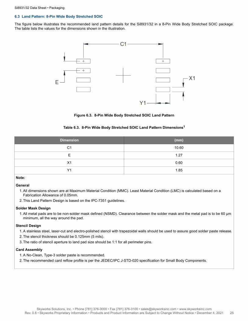
6.3 Land Pattern: 8-Pin Wide Body Stretched SOIC
The figure below illustrates the recommended land pattern details for the Si8931/32 in a 8-Pin Wide Body Stretched SOIC package.The table lists the values for the dimensions shown in the illustration.
Figure 6.3. 8-Pin Wide Body Stretched SOIC Land Pattern
Table 6.3. 8-Pin Wide Body Stretched SOIC Land Pattern Dimensions1
Dimension (mm)
C1 10.60
E 1.27
X1 0.60
Y1 1.85
Note:
General1. All dimensions shown are at Maximum Material Condition (MMC). Least Material Condition (LMC) is calculated based on a
Fabrication Allowance of 0.05mm.2. This Land Pattern Design is based on the IPC-7351 guidelines.
Solder Mask Design1. All metal pads are to be non-solder mask defined (NSMD). Clearance between the solder mask and the metal pad is to be 60 µm
minimum, all the way around the pad.
Stencil Design1. A stainless steel, laser-cut and electro-polished stencil with trapezoidal walls should be used to assure good solder paste release.2. The stencil thickness should be 0.125mm (5 mils).3. The ratio of stencil aperture to land pad size should be 1:1 for all perimeter pins.
Card Assembly1. A No-Clean, Type-3 solder paste is recommended.2. The recommended card reflow profile is per the JEDEC/IPC J-STD-020 specification for Small Body Components.
Si8931/32 Data Sheet • Packaging
Skyworks Solutions, Inc. • Phone [781] 376-3000 • Fax [781] 376-3100 • [email protected] • www.skyworksinc.com25 Rev. 0.8 • Skyworks Proprietary Information • Products and Product Information are Subject to Change Without Notice • December 4, 2021 25

6.4 Land Pattern: 8-Pin Narrow Body SOIC
The figure below illustrates the recommended land pattern details for the Si8931/32 in an 8-Pin Narrow Body SOIC package. The tablelists the values for the dimensions shown in the illustration.
Figure 6.4. 8-Pin Narrow Body SOIC Land Pattern
Table 6.4. 8-Pin Narrow Body SOIC Land Pattern Dimensions
Symbol mm
C1 5.40
E 1.27
X1 0.60
Y1 1.55
Note:1. This Land Pattern Design is based on IPC-7351 pattern SOIC127P600X173-8N for Density Level B (Median Land Protrusion).2. All feature sizes shown are at Maximum Material Condition (MMC) and a card fabrication tolerance of 0.05 mm is assumed.
Si8931/32 Data Sheet • Packaging
Skyworks Solutions, Inc. • Phone [781] 376-3000 • Fax [781] 376-3100 • [email protected] • www.skyworksinc.com26 Rev. 0.8 • Skyworks Proprietary Information • Products and Product Information are Subject to Change Without Notice • December 4, 2021 26

6.5 Top Marking: 8-Pin Wide Body Stretched SOIC
The figure below illustrates the top markings for the Si8931/32 in a 8-Pin Wide Body Stretched SOIC package. The table explains thetop marks shown in the illustration.
S i 8 9 X V
T T T T T TY Y WW
3
Figure 6.5. 8-Pin Wide Body Stretched SOIC Top Marking
Table 6.5. 8-Pin Wide Body Stretched SOIC Top Mark Explanation
Line 1 Marking: Customer Part Number
Si893X
X = Base part number• 1 = Differential output• 2 = Single-ended output
V = Insulation rating:• D = 5.0 kVrms
Line 2 Marking: TTTTTT = Mfg Code Manufacturing Code from the Assembly Purchase Order form.
Line 3 Marking:
YY = Year
WW = Work Week
Circle = 43 mils Diameter
Left-Justified
Assigned by the Assembly House. Corresponds to the year andwork week of the mold date.
Si8931/32 Data Sheet • Packaging
Skyworks Solutions, Inc. • Phone [781] 376-3000 • Fax [781] 376-3100 • [email protected] • www.skyworksinc.com27 Rev. 0.8 • Skyworks Proprietary Information • Products and Product Information are Subject to Change Without Notice • December 4, 2021 27

6.6 Top Marking: 8-Pin Narrow Body SOIC
The figure below illustrates the top markings for the Si8931/32 in an 8-Pin Narrow Body SOIC package. The table explains the topmarks shown in the illustration.
S i 8 9 X VC C Y Y WW
3
T T T T T T
Figure 6.6. 8-Pin Narrow Body SOIC Top Marking
Table 6.6. 8-Pin Narrow Body SOIC Top Marking Explanation
Line 1 Marking: Customer Part Number
Si893X = Isolator Amplifier Series
X = Base part number• 1 = Differential output• 2 = Single-ended output
S = Input Range:• A = ±62.5 mV• B = ±250 mV
V = Insulation rating:• B = 2.5 kVrms
Line 2 Marking:
CC = Country of Origin ISO Code Ab-breviation
YY = Year
WW = Work Week
Assigned by the Assembly House. Corresponds to the year and work weekof the mold date.
Line 3 Marking:
TTTTTT = Mfg Code
Circle = 19.7 mils Diameter
Left-Justified
Manufacturing Code from the Assembly Purchase Order form.
Si8931/32 Data Sheet • Packaging
Skyworks Solutions, Inc. • Phone [781] 376-3000 • Fax [781] 376-3100 • [email protected] • www.skyworksinc.com28 Rev. 0.8 • Skyworks Proprietary Information • Products and Product Information are Subject to Change Without Notice • December 4, 2021 28

7. Revision History
Revision 0.8
May, 2021• Added Automotive OPNs to 1. Ordering Guide.• Updated Figure 3.1 Voltage Sense Application on page 6.• Updated Table 4.4 Absolute Maximum Ratings1 on page 11.• Added Surge Voltage parameter to Table 4.8 VDE 0884-11 Insulation Characteristics1 on page 13.• Changed "60 mm" to "60 µm" in Solder Mask Design note in Table 6.3 8-Pin Wide Body Stretched SOIC Land Pattern Dimensions1
on page 25.
Revision 0.7
December, 2019• Updated Applications and Key Features on front page.• Updated 4. Electrical Specifications after full characterization.• Added section for Automotive Grade OPNs.• Updated Table 4.6 Insulation and Safety-Related Specifications on page 12.• Updated 6.6 Top Marking: 8-Pin Narrow Body SOIC.• Changed Si8932 Pin 6 from NC to GND.• Numerous clarifications throughout.
Revision 0.5
March, 2019• Updated specifications.• Added narrow body SOIC-8 package.
Revision 0.2
May, 2018• Corrections and clarifications.
Revision 0.1
January, 2018• Initial draft.
Si8931/32 Data Sheet • Revision History
Skyworks Solutions, Inc. • Phone [781] 376-3000 • Fax [781] 376-3100 • [email protected] • www.skyworksinc.com29 Rev. 0.8 • Skyworks Proprietary Information • Products and Product Information are Subject to Change Without Notice • December 4, 2021 29

Copyright © 2021 Skyworks Solutions, Inc. All Rights Reserved.Information in this document is provided in connection with Skyworks Solutions, Inc. (“Skyworks”) products or services. These materials, including the information contained herein, are provided by Skyworks as a service to its customers and may be used for informational purposes only by the customer. Skyworks assumes no responsibility for errors or omissions in these materials or the information contained herein. Skyworks may change its documentation, products, services, specifications or product descriptions at any time, without notice. Skyworks makes no commitment to update the materials or information and shall have no responsibility whatsoever for conflicts, incompatibilities, or other difficulties arising from any future changes.
No license, whether express, implied, by estoppel or otherwise, is granted to any intellectual property rights by this document. Skyworks assumes no liability for any materials, products or information provided hereunder, including the sale, distribution, reproduction or use of Skyworks products, information or materials, except as may be provided in Skyworks’ Terms and Conditions of Sale.
THE MATERIALS, PRODUCTS AND INFORMATION ARE PROVIDED “AS IS” WITHOUT WARRANTY OF ANY KIND, WHETHER EXPRESS, IMPLIED, STATUTORY, OR OTHERWISE, INCLUDING FITNESS FOR A PARTICULAR PURPOSE OR USE, MERCHANTABILITY, PERFORMANCE, QUALITY OR NON-INFRINGEMENT OF ANY INTELLECTUAL PROPERTY RIGHT; ALL SUCH WARRANTIES ARE HEREBY EXPRESSLY DISCLAIMED. SKYWORKS DOES NOT WARRANT THE ACCURACY OR COMPLETENESS OF THE INFORMATION, TEXT, GRAPHICS OR OTHER ITEMS CONTAINED WITHIN THESE MATERIALS. SKYWORKS SHALL NOT BE LIABLE FOR ANY DAMAGES, INCLUDING BUT NOT LIMITED TO ANY SPECIAL, INDIRECT, INCIDENTAL, STATUTORY, OR CONSEQUENTIAL DAMAGES, INCLUDING WITHOUT LIMITATION, LOST REVENUES OR LOST PROFITS THAT MAY RESULT FROM THE USE OF THE MATERIALS OR INFORMATION, WHETHER OR NOT THE RECIPIENT OF MATERIALS HAS BEEN ADVISED OF THE POSSIBILITY OF SUCH DAMAGE.
Skyworks products are not intended for use in medical, lifesaving or life-sustaining applications, or other equipment in which the failure of the Skyworks products could lead to personal injury, death, physical or environmental damage. Skyworks customers using or selling Skyworks products for use in such applications do so at their own risk and agree to fully indemnify Skyworks for any damages resulting from such improper use or sale.
Customers are responsible for their products and applications using Skyworks products, which may deviate from published specifications as a result of design defects, errors, or operation of products outside of published parameters or design specifications. Customers should include design and operating safeguards to minimize these and other risks. Skyworks assumes no liability for applications assistance, customer product design, or damage to any equipment resulting from the use of Skyworks products outside of Skyworks’ published specifications or parameters.
Skyworks, the Skyworks symbol, Sky5®, SkyOne®, SkyBlue™, Skyworks Green™, Clockbuilder®, DSPLL®, ISOmodem®, ProSLIC®, and SiPHY® are trademarks or registered trademarks of Skyworks Solutions, Inc. or its subsidiaries in the United States and other countries. Third-party brands and names are for identification purposes only and are the property of their respective owners. Additional information, including relevant terms and conditions, posted at www.skyworksinc.com, are incorporated by reference.
Portfoliowww.skyworksinc.com
Qualitywww.skyworksinc.com/quality
Support & Resourceswww.skyworksinc.com/support
Connecting Everyone
and Everything,
All the Time
Skyworks Solutions, Inc. | Nasdaq: SWKS | [email protected] | www.skyworksinc.comUSA: 781-376-3000 | Asia: 886-2-2735 0399 | Europe: 33 (0)1 43548540 |