rapid prototyping of a micro pump for microelectronic .../67531/metadc683248/m2/1/high...rapid...
TRANSCRIPT

SANDIA REPORT SAND96-2463 UC-705 Unlimited Release Printed May 1997
Rapid Prototyping of a Micro Pump for Microelectronic Applications
C. Channy Wong, Dahwey Chu, Sally L. Liu, Melanie R. Tuck, Douglas R. Adkins, Jeffry J. Sniegowski
Prepared by Sandia National Laborat Albuquerque, New Mexi

Issued by San& Laboratories, operated for the United States Department of E; ad ia Corporation. NOTICE: This 2 . vas prepared as an account of work sponsored by an agency of the United States Government. Neither the United States Govern- ment nor any agency thereof, nor any of their employees, nor any of their contractors, subcontractors, or their employees, makes any warranty, express or implied, or assumes any legal liability or responsibility for the accuracy, completeness, or usefulness of any information, apparatus, prod- uct, or process disclosed, or represents that its use would not infringe pri- vately owned rights. Reference herein to any specific commercial product, process, or service by trade name, trademark, manufacturer, or otherwise, does not necessarily constitute or imply its endorsement, recommendation, or favoring by the United States Government, any agency thereof, or any of their contractors or subcontractors. The views and opinions expressed herein do not necessarily state or reflect those of the United States Govern- ment, any agency thereof, or any of their contractors.
Printed in the United States of America. This report has been reproduced directly from the best available copy.
Available to DOE and DOE contractors from Office of Scientific and Technical Information P.O. Box 62 Oak Ridge, TN 37831
Prices available from (615) 576-8401, FTS 626-8401
Available to the public from National Technical Information Service U.S. Department of Commerce 5285 Port Royal Rd Springfield, VA 22161
NTIS price codes Printed copy: A03 Microfiche copy: A01

PoFtiOns of this document mag be illegible in electronic m e products Images are produced fiom the best available original dOr?umeXlL
SAND96-2463 Unlimited Release Printed May 1997
Rapid Prototyping of a Micro Pump for Microelectronic Applications
C. Channy Wong, Dahwey Chu, Sally L. Liu, Melanie R. Tuck,
Douglas R. Adkins, Jeff ry J. Sniegowski
Engineering Sciences Center and Microelectronics and Photonics Center
Sandia National Laboratories Albuquerque, NM 871 85
Abstract
A micro electro-hydrodynamic (EHD) injection pump has been developed using laser micromachining technology. Two designs have been fabricated, tested, and evaluated. The first design has two silicon parts with KOH-etched wells which are stacked on the top of each other. The wells are etched into one side of the wafer, and gold is deposited on the other side to serve as the pump electrodes. A Nd:YAG laser is used to drill an array of circular holes in the well region of both silicon parts. This creates a grid distribution with a square pattern. Next the well regions of the silicon parts are aligned, and the parts are bonded together using a Staystik thermoplastic. Together, the bonded silicon parts form the pump. The pump unit is then mounted into a ceramic package with a large hole drilled in the bottom of the package to permit fluid flow. Aluminum ribbon wire bonds are used to connect the pump electrodes to the package leads. Isolation of the metallization and wires is achieved by filling the package cavity and coating the wires with polyimide. When a voltage is applied to the electrodes, ions are injected into the working fluid, such as an organic solvent, thus inducing flow. The second design has the silicon parts oriented ‘back-to-back7 and bonded together with Stayform. A ‘back-to-back7 design will decrease the grid distance so that a smaller voltage is required for pumping. Experimental results have demonstrated that this micro pump can achieved a pressure head of about 287 Pa with an applied voltage of 120 V.

Acknowledgment
This work was supported by the United States Department of Energy under Contract DE-ACO4- 94AL85000 through the Laboratory Directed Research and Development (LDRD) Program. Micro pumps were fabricated at the DOE’S Microelectronics Development Laboratory and the testing were conducted at the Engineering Sciences Center Experimental Facility at Sandia National Laboratories. Their supports are really appreciated.
The authors would like to acknowledge Simone Smith, John White, and Nao Moore in assisting the construction of the micro pump and John Henfling and Zahid Mahmud for helping out the micro pump experiment. Many thanks to David Shen, Ronald Dykhuizen, Ken S . Chen, Vincent Amatucci and Timothy O’Hern for their valuable comments and discussions.
.. 11

Contents .. Acknowledgment 11 .......................................................................................................
Executive Summary ................................................................................................... vi
Rapid Prototyping of a Micro Pump for Microelectronic Applications
1 Introduction 1 1.1 Background 1 1.2 System Integration ............................................................................................ 1.3 Rapid Prototyping 2
............................................................................................................. .......................................................................................................
1 .............................................................................................
2 Laser Micromachining ............................................................................................ 2.1 Advantages of Laser Micromachining .............................................................. 2.2 Laser Micromachining Technology at Sandia ..................................................
3 Design of an EHD Injection Pump ......................................................................... 3.1 Electro-hydrodynamic Principle ...................................................................... 3.2 First Iteration: a Stacked Geometry .................................................................. 3.3 Second Iteration: a Back-to-back Geometry .....................................................
4 Test Results of the EHD Injection Pumps .............................................................. 4.1 Setup of the EHD Experiment .......................................................................... 4.2 Test Results ....................................................................................................... 4.3 Discussions on Recent Development ................................................................
3 3 3 5 5 9
13
17 17 17 18
5 Conclusions and Recommendations ....................................................................... 21
6 References ............................................................................................................... 23
A- 1 B- 1
APPENDIX A - Experimental Procedure ............................................................... APPENDIX B - LDRD Proposal ............................................................................
... 111
~
1.1 3.1 3.2 3.3 3.4 3.5 3.6 3.7
3.8 4.1 4.2
4.3
Figures
Schematic Diagram of an Active Cooling System ................................................
Cross-sectional Diagram of the Stacked Geometry Injection Pump ..................... Cross-sectional Photograph of Laser-drilled Holes ............................................... Cross-sectional Photograph of Assembled Stacked Pump .................................... Top View Photograph of the Assembled Stacked Injection Pump ........................ Cross-sectional Diagram of the Back-to-back EHD Pump .................................... Exit Hole Cracking and Damage when Laser Drilling Two Layers of Silicon and Stayform 421 between the Two Layers ............................................................ Cross-sectional Photograph of Clean Laser-drilled Holes without Cracking ........ Setup of the Micro Electro-hydrodynamic Injection Pump Experiment ............... Induced Pressure as a Function of Applied Voltage . (EHD Pump: 'Back-to-back', 0.004" Grid Size, Spacing, & Distance.) ...................................... Induced Pressure and Power Input as a Function of Applied Voltage of a Micro Pump (from the 3rd Design Iteration; Grid Distance-153 pm) ...............
Illustration of the Electro-hydrodynamic Principle ............................................... 2 5 9
10 10 11 13
14 15 17
18
19
iv

Tables
3.1 3.2
First Iteration EHD Pump Design (Stacked Version) -- Process Flow ................. Second Iteration EHD Pump Design (Back-to-back Version) -- Process Flow ...
12 16
V

Executive Summary
As the first phase of the system integration process of micro-electro-mechanical devices, a micro electro-hydrodynamic (EHD) injection pump has been developed using laser micromachining technology. Laser micromachining can deliver a faster processing time and is relatively cheaper for use in the development of a conceptional micro devices. Two designs have been fabricated, tested, and evaluated. The first design has two silicon parts with KOH-etched wells which are stacked on the top of each other. The wells are etched into one side of the wafer, and gold is deposited on the other side to serve as the pump electrodes.
A Nd:YAG laser is used to drill an array of circular holes in the well region of both silicon parts. This creates a grid distribution with a square pattern. Next the well regions of the silicon parts are aligned, and the parts are bonded together using a Staystik thermoplastic. Together, the bonded silicon parts form the pump. The pump unit is then mounted into a ceramic package with a large hole drilled in the bottom of the package to permit fluid flow. Aluminum ribbon wire bonds are used to connect the pump electrodes to the package leads. Isolation of the metallization and wires is achieved by filling the package cavity and coating the wires with polyimide. When a voltage is applied to the electrodes, ions are injected into the working fluid, such as an organic solvent, thus inducing flow.
The second design has the silicon parts oriented ‘back-to-back’ and bonded together with Stayform. A ‘back-to-back’ design will decrease the grid distance so that a smaller voltage is required for pumping. Experimental results have demonstrated that this micro pump can achieved a pressure head of about 287 Pa with an applied voltage of 120 V.

1 Introduction
1.1 Background
Recent advances in the fabrication of silicon micro-structures have created a new technology for the miniaturization of many structural, thermal and fluid flow devices such as pressure and temperature sensors, micro motors, and micro actuators. The characteristic length of these devices is on the order of microns. They can achieve high reliability and are relatively inexpensive to manufacture because they can be produced in a large quantities. This technology, known as Micro-Electro-Mechanical Systems or MEMS, will revolutionize manufacturing, sensing, and diagnostics processes because it can reduce the size of a device by several orders of magnitude. If incorporated into an engineering system, the integrated MEMS unit can be built smaller, lighter, smarter, and cheaper than current systems. Thus MEMS technology has the potential of changing the way we live and work in the future.
The MEMS silicon micro-structure technology has been advancing rapidly over the past decade. However most MEMS research has been focused on the fabrication and testing of single components. Very limited work exists in the integration of MEMS devices into an engineering system. Building and testing such systems is a complex and difficult task.
1.2 System Integration
The original goal of this research program focused on developing and demonstrating a process for system integration of micro-devices. System integration has many processes and may require several iterations between different processes. These processes include: project goal and definition, design and development, fabrication, testing and evaluation, and delivery of a final product. Because MEMS development is research intensive, several iterations between design and testing process are typically or usually needed in order to produce a final product.
The approach to speeding up the system integration process is to incorporate computational modeling into the design loop and by including mechanical analysis in electrical design considerations at an early phase of the system development. This will minimize the number of design iterations, thus speeding up the product’s design cycle time and reducing its costs. This intense and directed interdisciplinary teamwork is also part of the uniqueness of this program.
To demonstrate how the MEMS integration process would work, we are designing, building, and testing an active cooling system for microelectronics applications (Fig. 1.1). The integrated unit will have the following components: a field array of temperature sensors to locate local hot spots, thermally driven micro-actuators, micro-pumps and micro-channels. This cooling system can be considered as a single loop micro-heat
1

exchanger to remove heat from a hot spot region and reject heat at some other location where heating is less critical.
/ /
EHD Pump & Flow Control chip
Smart Inkgrated Cooling Module
Figure 1.1 Schematic Diagram of an Active Cooling System.
1.3 Rapid Prototyping
The manufacturing cost of MEMS can be low because many devices can be manufactured in one lot. Thus, the cost of MEMS devices is dominated by the development cost. In the MEMS research and development phase, current techniques to produce MEMS structures include silicon micromachining using wet and dry etching, excimer laser micromachining, and LIGA (Lithographie, Galvanoformung, Abformung, German words for lithography, electro-plating, and molding. LIGA is also known as deep-UV etching.) All these methods require high capital cost, special equipment, and facilities. Hence in order to reduce the development cost, MEMS researchers and engineers have been looking for ways to shorten the ‘research-to-development-production’ cycle and time.
Our initial effort is to develop and test single components and then follow-up with the system integration. Since this is an ambitious task, our desire is to rapidly prototype these single components and to evaluate our design concept quickly. This report addresses the design and fabrication of a micro electro-hydrodynamic (EHD) injection pump using laser micromachining and material bonding. This allows us to achieve a quick turn-around time and develop a cost effective prototyping process.
2
2 Laser Micromac hin i ng
2.1 Advantages of Laser Micromachining
Laser micromachining bridges the gap between the resolution obtainable by conventional mechanical machining operations and chemical micromachining techniques. Using conventional machining processes, it is extremely difficult, if not impossible, to produce machined components with structures several mils (1 mil c- 25 microns) in size with tolerances of a quarter of a mil. Chemical micromachining techniques allow much smaller structures (in micron size) to be produced; these techniques have limitations in the materials that can be machined and in obtaining high-aspect-ratio geometries. In general, chemical micromachining techniques are a planar technology and rely on isotropic etchants to remove the excess material. Thus, material is removed uniformly from the substrate in all directions. However using a chemical micromachining process to develop and fabricate a conceptional micro-device takes time and is relatively expensive.
For bulk micromachining processing, laser micromachining has the distinct advantage of being able to produce high aspect ratio geometries with micron, or several micron, resolution. In addition,-the laser process is applicable to a broad range of materials and the laser wavelength can be modified to insure optimum coupling of the laser radiation to the material being machined. The laser process also has a faster process time and is relatively cheaper for use in the development of a conceptional micro-device.
2.2 Laser Micromachining Technology at Sandia
Sandia has acquired Nd:YAG (Neodymium: Yttrium Aluminum Garnet) laser technology, a unique technology, that is well suited for rapid prototyping. Unlike excimer lasers that are expensive and have potential environmental, safety, and health concerns due to the toxic gases used, the Nd:YAG laser is more cost effective to acquire and to operate. Moreover the Nd:YAG laser will allow the operational wavelength to be converted to several frequencies from the near infrared portion of the spectra to the ultraviolet portion of the spectra.
The Nd:YAG laser system was originally designed to process silicon of varying thicknesses, hole diameters, and geometries. Initially all work was accomplished at the fundamental wavelength (A) of 1064 nm. Creation of through holes in the silicon (Si) at the wavelength of 1064 nm is done largely by melting the silicon. Most of the fabrication done on the micro pump uses this wavelength (1064 nm) for a quick turn-around time. Through various experimental procedures and cross-sectional evaluation, it was determined that the absorption coefficient at this wavelength for Si was not optimal for laser machining. However, the laser system could be modified to produce the second harmonic, with a wavelength of 532 nm. Second harmonic generation (SHG) was produced using intra- cavity frequency doubling with a non-linear crystal.
3

The development of SHG was done specifically to laser process silicon for two primary reasons. First, the absorption coefficient in silicon at the wavelength of 532 nm is approximately 2 times greater than at the wavelength of 1064 nm. Secondly, the focused spot size at this wavelength is =: 12 pm. Using the equation for spot size,
spot size = (wavelength x focal length /beam diameter)
we calculate the focused spot size for SHG to be half the diameter of the beam with a wavelength of 1064 nm. The combination of greater energy absorption in silicon at the wavelength of 532 nm combined with the significantly smaller focused spot size creates a mechanism of vaporization and ablation for removing silicon material. This is due to a significant increase in the absorbed power density. The calculated irradiance at the sample for the wavelength of 532 nm is equal to 5 . 8 ~ 1 0 ~ watt/cm2 based on a repetition rate of 4 kHz and a pulse width of 150 nsec. The wavelength of 532 nm also proved to be very efficient in laser machining silicon with minimal debris and side wall micro-cracking in the through hole.
The next major development in the laser system was to design a system capable of fourth harmonic generation (FHG) to produce an output beam in the ultraviolet at the wavelength of 266 nm. This would allow simultaneous drilling through Si and organics. The development of the fourth harmonic generation included a combination 4th harmonic crystal holder with focusing lenses, optical wavelength separator and ultraviolet up- collimator. The average output power at the wavelength of 266 nm was approximately 400- 600 milliwatts, and irradiance per pulse = 2 .35~10~ watt/cm*.
As a result of numerous process requirements, a laser system was developed with extensive machining capabilities, due mainly to the capability of utilizing wavelengths ranging from the near infrared, through the visible, to the ultraviolet spectrum.
4

3 Design of an EHD Injection Pump
Designing and fabricating a micro pump for microelectronic applications is a challenging task. The design requirement is to extract heat from the hot spot region in a multiple-chip module at about 30 watt/cm2. This requires a volumetric flow rate in a micro- channel to be in the order of 3 milliliters per minute. Several existing micro and conventional pump designs have been investigated. These include membrane pumps2-4 as well as pumps without moving parW7. Most pump design can achieve a pumping rate of several hundred microliters per minute and only a few design can reach a pumping rate of milliliters per minute.
3. I Elect ro- h yd rod y nam ic Principle
One fluid pump design that is very attractive in theory is an electro-hydrodynamic injection pump7, also known as an ion drag pump. The principle behind the ion drag pumps is as follows: consider two screen electrodes placed at a fixed distance apart inside a rectangular conduit with an insulating wall (Fig. 3.1). When an electrical potential is applied to the electrodes, charged particles are uniformly injected into a nonconductive fluid at the upstream electrode (x=O) and then collected at the downstream electrode (x=L). These charged particles are ions generated by a corona discharge. The motion of these charged particles, as they are traveling between the electrodes, will drag the fluid molecules along, thus creating a pumping motion.
x=o x=L I I
Z JL V
Figure 3.1 Illustration of the Electro-hydrodynamic Principlex.
5

Next in this section, we will derive a simple model to illustrate the interaction between the electric field and the induced flow. Interested readers should refer to Melcher (1981) for more detailed information on electro-mechanics.
The current density, Jxj associated with the ions discharge and fluid motion in the x- direction is as follows:
where pi , b, and v, are the charge density, mobility, and fluid velocity, respectively.
The first term corresponds to the current generated from the charged particles motion relative to the air. The second term corresponds to the current generated from the induced fluid motion. To simplify our analysis, we will neglect the diffusion and generation of charged particles in the fluid. If we assume that the electric field induced by charges in the fluid is relatively small compared to the electric field imposed by means of the electrodes,
This implies that for a constant applied voltage (V), the E field will increase with a decreasing separation distance (L).
To simplify this analysis, we will only consider a fully developed flow in the x- direction and the flow field is invariant in the z-direction. Hence we can treat the problem as a one-dimensional problem. The general solutions are of the form:
ap ax ? = J J y ) - i?x - = constant
This general solutions will satisfy the required governing equation which is the x- component of the Navier-Stokes equation.
6

The current density, J,, usually varies in the y-direction and can be determined at the inlet. However we can approximate the variation is relatively small and negligible, thus J, = J, and is uniform over the cross section. From Eq. (l), we can solve for the charged particle density, pi, and substitute into Eq. (4) to obtain a differential equation for the velocity profile:
The nonlinear expression in Eq. (5) can be reduced to a linear term by restricting attention to circumstances when bE, >> v, so that (bE,+ v,)-l G (bE,)-* - v,(bEJ2. Then Eq. (5) can be written as a linear ordinary differential with spatial varying coefficients:
Equation (6) can be re-arranged as:
where
K=F Pb E,
and
7

The boundary conditions are:
at y= 0, v, = 0
at y= d, v, = 0
Hence the solution for the fluid velocity field is as follows:
1
K
sinh Kd - sinh KY - sinh K (d - y ) sinh K d V,(Y) = 2 - 77 *
Since the electric Hartman number, He , is defined as: He =
we can express Eq. (10) as:
sinhHe - sinhH e($) - sinhHe( 1 - $) V,(Y 1 b dx sinh H e (1 1)
The pump characteristic is obtained by integrating Eq. (1 1) over the channel cross section (where d is the height and w is the width) and the volumetric flow rate, Qv, will be:
* d * w Qv = Vavg
where
The last term in Eq. (13) is always smaller than 1 for different electric Elatman number, H e . Its value spans from 0.0008 for He=O.l to 0.98 for H,=lOO. Hence the average fluid velocity with respect to pumping mostly depends on the square of the ratio, d/He. This implies:
8

As the separation distance between electrodes decreases, for a constant applied voltage, the E, field will increase (Eq. 2) and so does the average fluid velocity (Eq. 14). This analysis illustrates why micro electro-hydrodynamic pump is very attractive for our integrated system.
3.2 First iteration: a stacked geometry
The first pump design uses two stacked silicon wells which are laser drilled to form a grid and metallized on one side for electrical contact (Figure 3.2). The wells are formed with a KOH etch, and then drilled from the well side to create a grid structure. Hole sizes for the grid are about 0.003" to 0.004" (76 pm to 102 pm) in diameter and spaced about 0.008" to 0.01" (203 pm to 254 pm) apart (Figure 3.3). Well dimensions are 0.180" x 0.150" (4.57 mm x 3.81 mm) and 0.009" (229 pm) deep. Some are 0.012" (305 pm) deep. The bottom part is 0.340" x 0.340" (8.64 mm x 8.64 mm) and the top part is 0.3 10" x 0.340" (7.87 mm x 8.64 mm) to allow room at the edge for wire bonding. Staystik 383, a nonconductive thermoplastic, is used to join the top and bottom parts along the well perimeters. Using the same Staystik adhesive, the assembled unit is mounted into a 40 pin DIP (Dual-Inline Package) that has a 0.150" (3.8 1 mm) diameter hole laser drilled through the bottom of the package cavity (Figure 3.4). Aluminum ribbon wire (0.020" x 0.001" or 508 pm x 25 pm) is tacked on to the pump electrodes and connected to package leads (Figure 3.5). Polyimide (MicroSi 115) and Staystik 383 is used to fill the package cavity and to coat the wire bonds. This isolates the wires and metal layers to prevent shorting through the fluid at higher voltages. This was observed as the failure mechanism of
ribbon bonds
+ holes gold
-7
Figure 3.2 Cross Sectional Diagram of the Stacked Geometry Injection Pump.
9
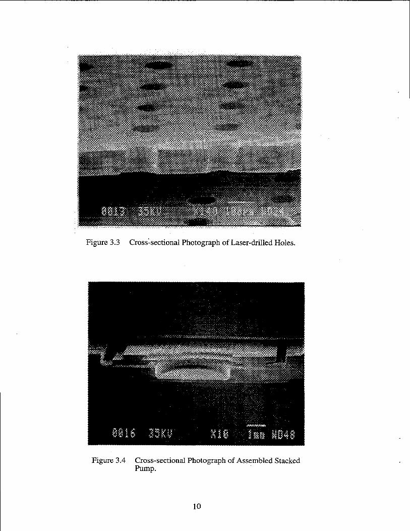
Figure 3.3 Crosskectional Photograph of Laser-drilled Holes.
Figure 3.4 Cross-sectional Photograph of Assembled Stacked Pump.
10

Figure 3.5 Top View Photograph of the Assembled Stacked Injection Pump.
uninsulated pumps. Wires are also attached to opposite sides of the package to eliminate shorting between wires.
Since lower voltages can be used to obtain pumping if the grid distance (Figure 3.2) is reduced, several pumps were constructed with a thinner top part (with thicknesses of 0.006" and 0.004", i.e. 153 pm and 102 pm). This reduces the grid distance from 0.013" (330 pm) to 0.007" (178 pm) and 0.005" (127 pm), respectively. Grid distance is equal to the top part thickness plus approximately 0.001" (25 pm) for the adhesive layer. The process flow for the stacked pump is given in Table 3.1.
Next these stacked micro-pumps were tested and evaluated for their performance. The working fluid being used for the tests is propanol, an organic solvent or alcohol. Preliminary test results show that these micro-pumps can pump fluid and produce a pressure head. The design with 0.004" (102 pm) holes and a 0.006" (152 pm) grid distance demonstrates that pumping starts at about 60 Volt, which is consistent with other electro- hydrodynamic micro-pump designs. More discussion of the testing and evaluation will appear in section 4. All these results have been fed back to the development process for any design improvement.
1 1

Table 3.1 First iteration EHD pump design (stacked version) -- process flow
Part description: Silicon pieces with KOH-etched wells
0 dimensions of bottom part: 0.340" x 0.340" (8.636 mm x 8.636 mm)
0 dimensions of top part: 0.310" x 0.340" (7.874 mm x 8.636 mm) [take a 'bottom' part and cut one edge in 0.030" (176.2 pm)]
0 both parts have gold deposited on front side (well side = back side)
0 thickness = 0.012" (304.8 pm)
0 well depth = 0.009" (228.6 pm) well size -. 0.180 x 0.150 (4.572 mm x 3.81 mm)
1. drill grid into top and bottom parts
wavelength = 1064 nm with 02, from back (well) side
hole size = 0.003" or 0.004" (76.2 pm or 101.6 pm) spacing = 0.008" or 0.01" (203 pm or 254 pm)
0 ultrasonic clean to remove debris
2. thin top part to decrease grid distance (top part is 0.004" or 0.006", i.e. 101.6 pm or 152.4 pm)
optional step; smaller grid distance + less voltage required for pumping
3. drill 0.150' (3.81 mm) diameter hole in center of package cavity (40 pin DIP)
package cavity = 0.370" x 0.370" (9.398 mm x 9.398 mm)
4. assemble pump
join top and bottom parts using Staystik 383 (non-conductive thermoplastic)
0 apply Staystik to the edge of the top part (along well perimeter)
aligning parts properly shodd also align pump grids (three sides should match up)
0 cure: 160 "C, 10 min.
5. part attach apply Staystik to the bottom of pump unit (back edge of bottom part)
align grids over hole in package
0 cure: 160 OC, 10 min.
6. wire bond: Al ribbon wire
0 thickness = 1 mil (25.4 pm), width = 20 mil (508 pm)
bond bottom part to pin 1, top part to pin 2 1
7. isolation of metallization and wires
fill package cavity and coat wire bonds with Staystik 383 or polyimide (MicroSi SP115) 0 allow to air cure & reapply insulative material to fill any gaps which formed during air cure
0 cure: 160 O C , 10 min. (Staystik); 175 "C, 1 hr (polyimide)
12
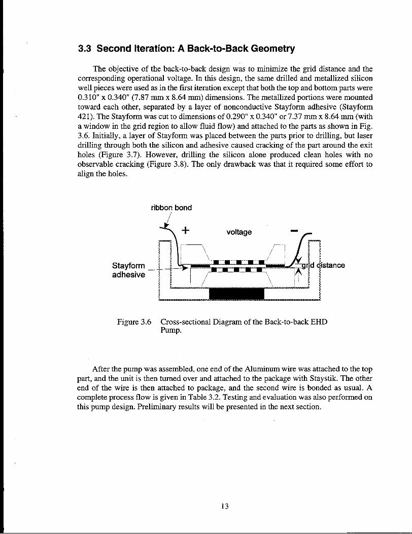
3.3 Second Iteration: A Back-to-Back Geometry
The objective of the back-to-back design was to minimize the grid distance and the corresponding operational voltage. In this design, the same drilled and metallized silicon well pieces were used as in the first iteration except that both the top and bottom parts were 0.310" x 0.340" (7.87 mm x 8.64 mm) dimensions. The metallized portions were mounted toward each other, separated by a layer of nonconductive Stayform adhesive (Stayform 421). The Stayform was cut to dimensions of 0.290" x 0.340" or 7.37 mm x 8.64 mm (with a window in the grid region to allow fluid flow) and attached to the parts as shown in Fig. 3.6. Initially, a layer of Stayform was placed between the parts prior to drilling, but laser drilling through both the silicon and adhesive caused cracking of the part around the exit holes (Figure 3.7). However, drilling the silicon alone produced clean holes with no observable cracking (Figure 3.8). The only drawback was that it required some effort to align the holes.
ribbon bond / 5+ voltage
Stayform istance adhesive
Figure 3.6 Cross-sectional Diagram of the Back-to-back EHD Pump.
After the pump was assembled, one end of the Aluminum wire was attached to the top part, and the unit is then turned over and attached to the package with Staystik. The other end of the wire is then attached to package, and the second wire is bonded as usual. A complete process flow is given in Table 3.2. Testing and evaluation was also performed on this pump design. Preliminary results will be presented in the next section.
13

Figure 3.7 Exit Hole Cracking and Damage when Laser Drilling Two Layers of Silicon and Stayform 421 between the Two Layers.
14

Figure 3.8 Cross-sectional Photograph of Clean Laser-drilled Holes without Cracking.
15 ,
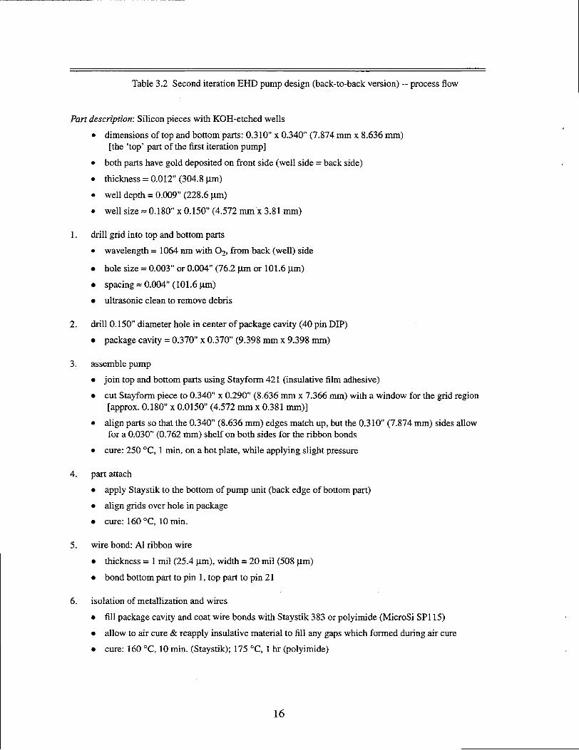
Table 3.2 Second iteration EHD pump design (back-to-back version) -- process flow
Part description: Silicon pieces with KOH-etched wells
1.
2.
3.
4.
5.
6.
dimensions of top and bottom parts: 0.310" x 0.340' (7.874 mm x 8.636 mm)
both parts have gold deposited on front side (well side = back side)
thickness = 0.012" (304.8 pm)
well depth = 0.009'' (228.6 pm)
well size = 0.180" x 0.150" (4.572 mm x 3.81 mm)
[the 'top' part of the first iteration pump]
drill grid into top and bottom parts
0 wavelength = 1064 nm with 02, from back (well) side
hole size = 0.003" or 0.004" (76.2 pm or 101.6 pm) spacing = 0.004" (101.6 pm)
ultrasonic clean to remove debris
drill 0.150" diameter hole in center of package cavity (40 pin DIP) package cavity = 0.370' x 0.370' (9.398 mm x 9.398 mm)
assemble pump join top and bottom parts using Stayform 421 (insulative film adhesive)
cut Stayform piece to 0.340" x 0.290" (8.636 mm x 7.366 mm) with a window for the grid region [approx. 0.180' x 0.0150" (4.572 mm x 0.381 mm)]
0 align parts so that the 0.340 (8.636 mm) edges match up, but the 0.310" (7.874 mm) sides allow for a 0.030" (0.762 mm) shelf on both sides for the ribbon bonds
cure: 250 "C, 1 min. on a hot plate, while applying slight pressure
part attach apply Staystik to the bottom of pump unit (back edge of bottom part)
align grids over hole in package
cure: 160 "C, 10 min.
wire bond: A1 ribbon wire
thickness = 1 mil (25.4 pm), width = 20 mil (508 pm)
bond bottom part to pin 1, top part to pin 21
isolation of metallization and wires
fill package cavity and coat wire bonds with Staystik 383 or polyimide (MicroSi SP115) allow to air cure & reapply insulative material to fill any gaps which formed during air cure
cure: 160 "C, 10 min. (Staystik); 175 "C, 1 hr (polyimide)
16
4 Test Results of the EHD Injection Pumps
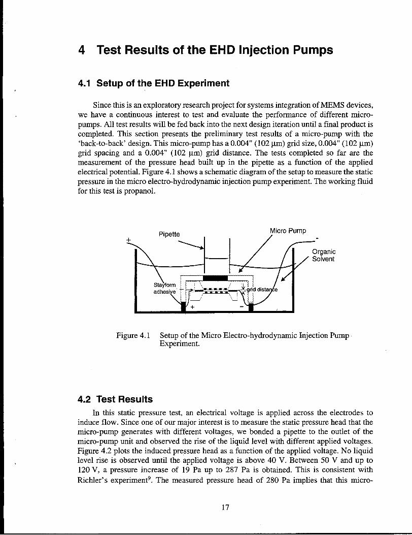
4.1 Setup of the EHD Experiment
Since this is an exploratory research project for systems integration of MEMS devices, we have a continuous interest to test and evaluate the performance of different micro- pumps. All test results will be fed back into the next design iteration until a final product is completed. This section presents the preliminary test results of a micro-pump with the 'back-to-back' design. This micro-pump has a 0.004" (102 pm) grid size, 0.004" (102 pm) grid spacing and a 0.004" (102 pm) grid distance. The tests completed so far are the measurement of the pressure head built up in the pipette as a function of the applied electrical potential. Figure 4.1 shows a schematic diagram of the setup to measure the static pressure in the micro electro-hydrodynamic injection pump experiment. The working fluid for this test is propanol.
PiDette Micro Pump 1
Organic Solvent
Figure 4.1 Setup of the Micro Electro-hydrodynamic Injection Pump Experiment.
4.2 Test Results In this static pressure test, an electrical voltage is applied across the electrodes to
induce flow. Since one of our major interest is to measure the static pressure head that the micro-pump generates with different voltages, we bonded a pipette to the outlet of the micro-pump unit and observed the rise of the liquid level with different applied voltages. Figure 4.2 plots the induced pressure head as a function of the applied voltage. No liquid level rise is observed until the applied voltage is above 40 V. Between 50 V and up to 120V, a pressure increase of 19 Pa up to 287 Pa is obtained. This is consistent with Richler's experiment9. The measured pressure head of 280 Pa implies that this micro-
17
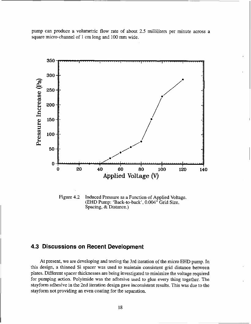
pump can produce a volumetric flow rate of about 2.5 milliliters per minute across a square micro-channel of 1 cm long and 100 rmn wide.
0 20 40 60 80 100 120 140 Applied Voltage (V)
Figure 4.2 Induced Pressure as a Function of Applied Voltage. (EHD Pump: 'Back-to-back', 0.004" Grid Size, Spacing, & Distance.)
4.3 Discussions on Recent Development
At present, we are developing and testing the 3rd iteration of the micro EHD pump. In this design, a thinned Si spacer was used to maintain consistent grid distance between plates. Different spacer thicknesses are being investigated to minimize the voltage required for pumping action. Polyimide was the adhesive used to glue every thing together. The stayform adhesive in the 2nd iteration design gave inconsistent results. This was due to the stayform not providing an even coating for the separation.
18
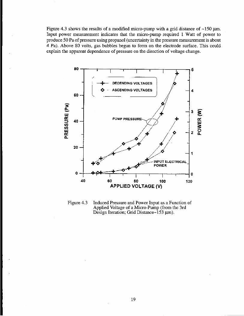
Figure 4.3 shows the results of a modified micro-pump with a grid distance of -150 pm. Input power measurement indicates that the micro-pump required 1 Watt of power to produce 50 Pa of pressure using propanol (uncertainty in the pressure measurement is about 4 Pa). Above 80 volts, gas bubbles began to form on the electrode surface. This could explain the apparent dependence of pressure on the direction of voltage change.
BO
60 - (P h
w e => 40 v) u) w L
Y
20
0
L I I 1 I I I - 5
-
1
/ 1- I
yw INPUT ELECTRICAL- -.re #+’ POWER
c --*-=+-- I I 1 0 I I
40 60 80 100 1 20 APPLiED VOLTAGE (V)
Figure 4.3 Induced Pressure and Power Input as a Function of Applied Voltage of a Micro-Pump (from the 3rd Design Iteration; Grid Distance- 153 pm).
19

20

5 Conclusions and Recommendations
As part of a system integration project of micro-devices, we have developed and demonstrated an electro-hydrodynamic injection micro pump using a laser micromachining technology. Our goal is to rapidly prototype and test single components so that we can speed up the development-to-production cycle. Eventually our deliverable will be an active built-in cooling system for microelectronics applications. Two designs have been investigated. The first design has the silicon parts stacked on top of each other and the second design has the silicon parts bonded back-to-back. A Nd:YAG laser is used to drill an array of circular holes in the well region of both silicon parts. This creates a grid distribution with a square pattern. The purpose of the second design is to reduce the grid distance so that a smaller voltage is required to induce flow. Preliminary results show that the second design qualitatively generates a higher pressure head. More tests are underway to further evaluate the two designs and also the influence of different grid size, grid spacing, grid distance, and hole size. For the micro-pump bonded ‘back-to-back‘ with 0.004” (102 pm) spacing, an induced pumping pressure of 287 Pa was achieved with 120 V.
21

22

6 References ’C . C. Wong, D. Chu, S. L. Liu, M. R. Tuck, Z. Mahmud, V. Amatucci, “Rapid
prototyping of a micro pump with laser micro-machining,” SPIE paper 2642-1 8, Micromachining and Microfabrication 1995, Austin TX, October 23-24 1995.
2H. T. G. Van Lintel, E C. M. Van De Pol, and S. Bouwstra, “A piezoelectric micropump based on micromachining of silicon,” Sensors and Actuators, Vol. 15, pp. 153- 167,1988.
3S. Miyazaki, T. Kawai, and M. Araragi, “A piezo-electric pump driven by a flexural progressive wave,” Proceedings of IEEE MicroElectroMechanical Systems, Nara, Japan, pp. 283-288, Jan./Feb. 1991.
4R. Zengerle, A. Richter, and H. Sandmaier, “A micro membrane pump with electrostatic actuation,” Proceedings of IEEE MicroEZectroMechanicaZ Systems, Travemunde, Germany, pp. 19-24, February 1992.
’S. E Bart, L. S. Tavrow, M. Mehregany, and J. H. Lang, “Microfabricated electrodydrodynamic pumps,” Sensors and Actuators, A. Physical, Vol. A2 1-23, pp. 193- 197,1990.
6G. Fuhr, R. Hagedorn, T. Muller, W. Benecke, and B. Wagner, “Microfabricated electrohydrodynamic (EHD) pumps for liquid of higher conductivity,” Journal of MicroElectroMechanical Systems, Vol. 1, No. 3, pp. 141-146, September 1992.
7A. Richter and H. Sandmaier, “An electrodydrodynamic micropump,” Proceedings ofIEEE MicroElectroMechanical Systems, Napa Valley, CA, pp. 99-104, February 1990.
‘J. R. Melcher, Continuum Electromechanics, MIT Press, Cambridge, Massachusetts, 198 1.
9A. Richler, A. Plettner, K. A. Hofmann, and H. Sandmaier, ““Electrohydrodynamic pumping and flow measurement,” Proceedings of IEEE MicroElectroMechanical Systems, Nara, Japan, pp. 271-276, Jan./Feb. 1991.
23

24

Appendix A - Experimental Procedure
A.l STANDARD OPERATING PROCEDURE
A.1 .I Prerequisites When preparing for the micro pump experiment, perform the following steps: a. Solder leads to pump. b. Adhere discharge tube to pump with hi-peel (orange) epoxy. c. Insulate pins with leads with epoxy. Let cure for 24 hours.
Before experiment, the authorized user shall familiarize himherself with the equipment schematics given in Figure 4.1 and be alert where the fire extinguisher is. Operator Checklists are in Table A. 1.
A.1.2 Procedure
I. Pre-run Adjustments
1. Set-up Wire power supply to pump. Place pump in the organic solvent such as propanol.
2. Inspection Prior to the test, the apparatus should be inspected. Items to look for are: (a) the micro pump is completely submerged, (b) there are no loose connections, (c) place a metal sheet over the container. If anything suspect is found, it must be rectified before running the experiment. Also, the lab should be checked for good housekeeping so that in the event of an emergency obstacles do not block critical paths.
11. Test Operation
1. Turn on power supply. 2. Adjust power supply to the desired setting. 3. Gather data, i.e. flow rate, pumping pressure, and voltage. 4. Turn off power at the conclusion of data collection.
111. System Shutdown
1. Unplug the power supply. 2. Disconnect the micro pump from power supply.
IV. Any Abnormal Event
1. Turn off power. 2, Unplug the power supply.
A- 1

A.1.3 Emergency Procedures
Because of the safe design of the experiment, the hazards have been minimized. The identifiable hazards that remain are due to operator error or failure of a part of the system. Below is a list of possible accidents, our planned prevention techniques and the planned response. In case of fire, injury, or any other emergency, call 91 1. Then call 15 12 Manager / 1515 Manager, Building 865 ES&H Coordinator, and 1500 Center ES&H Coordinator.
I. Fire An accident may happen such that the micro pump may be pulled out of the liquid or
the container may be knocked over such that the ignition may occur. Precaution has been taken to prevent any ignition. The precaution steps are listed as follows: (1) the micro EHD pump experiment will be performed under a fume hood in Room 13, (2) the micro EHD pump will be completely submerged in the organic solvent during the experiment to prevent any continuous supply of oxygen, (3) wooden blocks or sand bags will be placed around the small container to prevent any knock over, (4) the small container with wooden blocks or sand bags will be placed on a bigger, fatter pan to contain any spilling, (5) the micro EHD pump and the wiring will be tied down so that the micro pump will not be accidently pulled out of the liquid. If an ignition occurs, the burning will confined within the small container and will extinguish quickly because the container will be covered with a sheet of metal to cut off oxygen supply. Be alert where the fire extinguisher is and use the fire extinguisher if needed. If there is fire in the pan, use fire extinguisher.
A.1.4 Follow-Up Actions
In the event that there is an unforeseen accident, a root cause analysis will be done. Department 15 12 and 15 15 Managers are responsible for writing the report.
A.2 WASTE DISPOSAL
Any waste generated or recovered from the system will be sent to waste operations through a Chemical Waste Disposal Request in accordance with the Sandia ES&H Manual. All waste must be sent to waste operations within 60 days of being declared waste.
A-2

Table A.l Operator Checklists
Micro Electrohydrodynamic Injection Pump Operation:
1 .O Pre-run Adjustments 1.1 1.2 1.3 1.4 1.5
1.6 1.7 1.8 1.9
Power supply is off and disconnected Place the micro pump in a container Put the container onto a fatter, bigger pan Place wooden blocks or sand bags around the container Take the units (container, blocks, and pan) and place them in the hood
Turn on the exhaust fan of the hood Pour organic solvent into the container Make sure the micro pump is completely submerged Use syringe to extract out any air
1.10 Place a flame suffocation metal sheet on top to cover up the container
1.1 1 Wire power supply to micro pump 1.12 Tie down the wiring and the micro pump 1.13 Check all electrical connections
2.0 Experiment Operation 2.1 Turn on power supply 2.2 2.3 Collect data 2.4 Turn off power supply
Adjust power supply to the desired setting
3.0 System Shutdown 3.1 Unplug the power supply 3.2 Disconnect the micro pump from power supply 3.3 Pour the organic solvent back into a safe container
Signature Date
Comments :

A-4
Appendix B - LDRD FY95 PROPOSAL
Project Title: System Integration of MicroElectroMechanical Devices ~
Responsible Project Manager (PM): C. Channy Wong, 1554 ~~~ ~~ ~~
Vincent Amatucci, 1553, Dahwey Chu, 1333, Jeffrey Payne, 1554, Jeffry Sniegowski, 1325, C. Channy Wong, 1554. PrincipalInvestigator(s):
Abstract (Nature of Work): The silicon microstructure technology, also known as MicroElectroMechanical System (MEMS),
has evolved rapidly over the past decade. However most MEMS research has been focused on fabrication and single component testing. Very limited work has been performed to integrate these MEMS devices into engineering systems and to investigate their performance. Such a system integration effort is a challenging task and is required to make the MEMS devices more widely acceptable.
This research project will focus on developing a system integration process for MEMS devices. This integration process would involve the following phases: project goal and definition, design and devel- opment, fabrication, test and evaluation, and final product development. Because of the exploratory nature of this work, a few iterations are probably needed in order to achieve a satisfactory final product. We believe that the integration process will be expedited if computational modeling is incorporated into the design loop. To demonstrate how this integration would work, we will design and build an active cooling system for microelectronics application. It will have the following components: a field array of temperature sensors to locate local hot spots, thermally driven micro-actuators, micro-pumps and micro-channels. This cooling sys- tem can be considered as a 2-loop heat exchanger. The operational sequence would be as follows: if the tem- perature increases beyond an acceptable limit, the temperature sensor will relay a signal to turn on a cooling pump and actuator. This will initiate the coolant flow to remove heat away from the multichip module or printed circuit board.
This research project involves multiple disciplines including electrical engineering as well as tradi- tional engineering science disciplines. Moreover the flow physics in this microscale level may involve non- continuum mechanics that requires particle dynamic simulations.Thus the proposed work will cover not only all aspects of experimental processes (design, fabrication, and testing) but also the full range of computa- tional modeling including continuum, transitional, and free-molecular flow regimes. This multi-discipline research can only be carried out at Sandia due to our unique combination of engineering capability.
Previous Year’s Accomplishments (2nd & 3rd Year Renewals Only): NIA - This is a new proposal.
Work Proposed for Next Year: During the first year, our primary effort will be to design and develop each of the discrete elements
in the cooling system. Then we will test and analyze the performance of each of these micro-devices. In a parallel effort, we will define the flow characteristics and the requirements for the micro-channels and pumps. When the results of the tests and computational simulations are available, we will update the component specifications and improve the design of the integrated system, if necessary. At the end of the first year, we will finalize the design and layout of the active cooling system and prepare for fabrication.
B-1

Introduction
iaturization of many structural, thermal and fluid flow devices such as pressure and temperature sensors, micromotors, and micro-actuators. The characteristic length of these devices is on the order of a micron. They are very reliable and inexpensive to manufacture. This technology, known as MicroElectroMechanical Systems or MEMS, will revolutionize manufacturing, sensing, and diagnostics processes because it can reduce the size of a device by several orders of magnitude. If incorporated into an engineering system, the integrated MEMS unit can be built smaller, lighter, and smarter. This new MEMS technology will soon affect our daily lives just as microelectronics technology does today. Its impact on U.S. economy will be enormous.
The MEMS silicon microstructure technology has developed rapidly over the past decade. However most MEMS research has been focused on fabrication and testing of single components. Very limited work exists to integrate these MEMS devices into an engineering system and investigate their performance. This is a difficult task.
Recent advances in the fabrication of silicon microstructures have created a new technology for the min-
This proposed research project will focus on developing and demonstrating a process for system inte- gration of the micro-devices. System integration has many processes and may require several iterations between different processes. The processes are: project goal and definition, design and development, fabrica- tion, testing and evaluation, and final product. Because this is an exploratory research project, several itera- tions between design and testing process are probably needed in order to achieve a final product. Our goal is to speed up the process by incorporating computational modeling into the design loop and by including mechanical analysis in electrical design considerations at an early phase of the system development. This will minimize the number of design iterations. This type of strong interactions and teaming between multi- ple disciplines is part of the uniqueness of this project.
To demonstrate how this system integration works, we propose to design and build an active liquid cool- ing system with temperature sensors for microelectronics application. This integrated cooling system, when developed, will help solve thermal management problems that currently exist in microelectronics packaging. Such a system would consists of the following components: a field array of temperature sensors to locate hot spots, thermally driven micro-actuators, micro-pump and micro-channels to direct the flow which would also serve as a heat exchanger for heat removal.
This research project involves multiple disciplines including electrical as well as mechanical engineer- ing disciplines. Moreover, it is probable that the flow physics at this micro-scale level will involve non-con- tinuum mechanics that requires particle dynamic simulations. Thus the proposed work will cover not only all aspects of experimental processes (design, fabrication, and testing) but also the full range of computational modeling including continuum, transitional, and free-molecular flow regimes. This multi-disciplinary research can only be carried out at Sandia.
Scientific and Technical Soundness Most of the existing work in MEMS development is in the area of fabrication and testing of single com-
ponents. Much effort is needed in the area of system integration. System integration of microelectromechan- ical devices is not an easy task and involves different processes (Figure B.l).This project will cover work throughout the research and development cycle, starting with a design goal and ending with a deliverable product. Usually, several iterations between design and testing process are needed in order to achieve a final product. Our goal is to speed up the process and minimize the number of iterations by incorporating compu- tational modeling into the design loop and including mechanical analysis in electrical design considerations at an early phase of the system development. To demonstrate how the integration process is done, we pro- pose to develop and fabricate an active liquid cooling system for microelectronics application. Thus, this cooling system becomes a test vehicle for system integration of micro-devices. By building and testing this integrated unit, we prove the compatibility, capabilities, and performance of these microelectromechanical devices.
The proposed active cooling system is a closed-loop, electrical powered unit and has the following dis- crete elements: temperature sensors, flow channels, thermally driven actuators, and pumps (Figure B.2).
B -2

Computational Modeling
Design Process
f
Figure B. 1 Flow Chart of the System Integration Process
Each individual component either has been previously developed or is currently being checked out within micro-fabrication capabilities at Sandia. Specifically, the temperature sensing elements can be made of sili- con diodes which have already been well characterized for temperature measurements. Micro-channels and thermally driven micro-actuators have been fabricated and checked out for other applications (Ref. 1). The micro-pump being considered for use in this system is based on an ElectroHydroDynamic (EHD) pumping technique. This technique has been proven elsewhere (Ref. 2) and can be readily incorporated into the pro- posed system, with present micromachining capabilities. The required fabrication technology already exists in-house at Sandia's Microelectronics Development Laboratory (MDL). The present effort is then to incor- porate these components into a closed-loop integated modular system.
I' I
flow channels t- heat out
Figure B.2 A Schematic Diagram of the Active Cooling System
When integrating these micro-devices together as a unit, some modifications are needed to satisfy the design specifications. (For example, when setting a design goal of heat removal rate at 100 Wh'. a typical peak thermal loading for the next generation microelectronic module to be used in weapons and supercom- puters, we might need to slightly modify the design to meet this requirement.) A few design considerations are: What is the needed geometry of the flow channels and its flow rate? Does the pump require multiple stages? Can the temperature sensor and other components interface well with each other and provide ade- quate responses? These are the engineering questions that we have already asked but can only be answered by actually building an integrated unit.
Since the micro-pump is based on the ElectroHydroDynamic principle, simulating the flow inside the pump requires modeling the electrostatic forces with an advanced numerical flow solver. Theoretically, the pump works in the following matter. Convection occurs when a traveling electromagnetic wave is applied across a fluid media in which an electrical conductivity or permittivity gradient exists. This inhomogeneous state of the electrical property of the fluid can be generated by local heating. Thus, in order to model the flow in the pump, we need to resolve the velocity and temperature fields in detail. This type of modeling is state- of-the-art research in fluid dynamics.
B -3
When working with this system integration process, we will address two technical issues. The first one corresponds to how different the fluid flow and heat transfer in the micro-scale environment (on the order of 1 to 10 pm) will be from macro-scale problems. At this length scale, the dominant flow physics may be dif- ferent. The length scale may be so small that non-continuum mechanics and particle dynamic simulation will have to be considered (which can be modeled with Direct Simulation Monte Carlo technology). At present, the preliminary design work will be based on the technical knowledge of the macro-scale level (on the order of 0.01 to 1 m). When a prototype of the integrated system is built, it will be tested and evaluated. The test results will be fed back into the development loop for a design modification. The second technical issue is associated with the difficulty of fabricating all components into a single modular unit and ensuring system reliability at the same time. This is not an easy task but is also needed. System integration is a crucial step, bringing the MEMS technology into the next higher level - for use in general engineering practice. This crucial step in MEMS technology is what we intend to contribute in this LDRD project.
Before proceeding to develop and fabricate the integrated unit, we will first design, fabricate, and test each component separately. This shake-down process will help us to identify and fix any potential problem areas early and more effectively. We expect this process will be completed before the end of the first year. Then we will design and fabricate a prototype of the integrated unit. Next testing and evaluation will be per- formed on this unit. The test results will be fed back into the development process for design improvement.
At the end of the project, we will have established a system integration process for the micro-electro- mechanical industry. We will also have a deliverable product - an active cooling system with built-in temper- ature sensors for microelectronic application. This active cooling system is desperately needed in the elec- tronics industry.
Creativity and Innovation System integration is new in microelectromechanical systems (MEMS) technology development. The
creativity of this project lies in the effort to combine discrete MEMS devices into a closed-loop engineering system. This integrated unit is highly compact due to its micromachining nature. It is reliable and capable of running unattended with the built-in sensing devices and the associated control mechanisms. These MEMS devices are relatively cheap to manufacture because of the maturity of the micro-fabrication methods. The innovation of the project is: (1) the use of computational simulation to expedite the ‘design-to-production’ processes, and (2) the system approach to create a micro-machined, active cooling module for microelec- tronics application. Thermal management in the multichip module is an important design issue that many electronic engineers face today. Incorporating an active cooling device would be a large step forward to enable improved system architecture and performance.
by building an active cooling module, the present approach also produces a valuable product for microelec- tronics application. Since most of the proposed discrete elements have been fabricated and tested at Sandia, our approach is reasonable. With a clearly defined goal in mind, strong interaction, and good team work at the early design phase, we are very confident with the success of the project.
There are a few risks in this endeavor. First the fabrication for the integrated system that consists of mul- tiple components, has not been done before at Sandia. It will require some careful thinking and engineering analysis. Second, the performance of the integrated system may be different than what is anticipated. The present fluid flow design is based on the knowledge of the macroscale level (in the order of meter). Fluid and thermal flow in a microscale level (in the order of micron) may be different and may require more detailed investigations using non-continuum techniques. We are prepared to analyze continuum as well as non-con- tinuum fluid dynamics if necessary.
Though the focus of this proposed project is to develop and demonstrate a system integration process,
Project Plan Schedule
Complete the preliminary design of the flow channels, actuator, and pumps - December 1994, Design experiments to check out the performance of each discrete component - March 1995, Perform computational simulation to investigate the dominant flow physics for design improvement - June 1995,
B -4
Fabricate and build each discrete component; test and evaluate their performance - August 1995, Review the earlier design and complete the layout of the first prototype of the integrated unit - September 1995,
Fabricate and build the first prototype of the integrated unit - December 1995, Test and evaluate the performance of the first prototype of the integrated unit - March 1996, Publish a SAND report on design, fabrication, and testing of the micro-devices - July 1996. Improve the design, fabricate and test the final version of the active cooling system - August 1996, Publish a SAND report on the system integration process- September 1996.
StafJing Vincent Amatucci (1553): Vincent will design and conduct experiments to test and evaluate the performance of the micro-devices. He has extensive experience performing experimental work in fluid mechanics and heat transfer. Dahwev Chu (1333): Dahwey will design and fabricate the micropumps and microchannels. He has been actively working on microelectronic packaging in the past 6 years. Jeffrev L. Pavne (15541: Jeff will apply computational simulation techniques to characterize the flow in the active cooling system. He has computational simulation experience in both continuum and non-continuum flows. Jeffrv J. Sniegowski (13251: Jeff will consult on the design and fabrication of the MEMS devices. He has 9 years of design and fabrication experience in micromechanics technology for sensors and actuators. C. Channv Wono (15541: Channy will manage the project, perform analytical modeling of the flow, and lead the team to build the active cooling system for system integration. He has worked on fluid dynamics and heat transfer problems for seventeen years. He has experience in incompressible swirling flow in nuclear reactor engineering, two-phase flow for nuclear reactor safety, hydrogen combustion, and hypersonic reentry flow.
Budget (total FY95 = $395K)
Staff FTE LC
Vincent Amatucci 0.3 50k Dahwey Chu 0.5 70k Jeffrey L. Payne 0.2 30k Jeffry J. Sniegowski 0.1 17k C. Channy Wong 0.4 59k
DCs of $70k are requested for IT95 to pay for laboratory supplies ($8K), masks ($lOk), contract labor in the fabrication facilities ($30k) and test facilities ($17k), and travel ($5K). SC of 21k is for use of the LAN in 1500.
Programmatic Impact
devices such as pressure and temperature sensors, motors, and actuators by several orders of magnitude. This technological advancement will revolutionize the manufacturing, sensing, and diagnostics industries. If incorporated into an engineering system, the integrated unit can be built smaller, lighter, cheaper, and smarter. This new MicroElectroMechanical (MEMS) technology will soon affect our daily lives and have substantial impact on U.S. economy just as microelectronics technology does today.
This system integration of micro-devices brings MEMS research to a new, higher level for broad-based engineering applications. It will also advance technology in other research areas that are important to engi- neering science research at Sandia. A few example are: (1) field-array sensing, (2) simultaneous measure- ment of state variables such as velocities, pressure, and temperature, and (3) diagnostic of a rapid processes.
The proposed LDRD would involve close teaming between two engineering disciplines and would sup- port continued core competencies at Sandia. The effort would position Sandia as a national leader, not only in MEMS technology but also in the implementation and engineered systems aspect of these devices. With- out question, a project such as this would help move MEMS technology out of the laboratory and into com- mercial use which would, in turn, open up exciting new market opportunities for Sandia as a national
The silicon microstructure technology can miniaturize many existing structural, thermal and fluid flow
B-5

laboratory.
Signatures C. Channy Wong, 1554, PI, PM
Vincent Amatucci, 1553, PI
Dahwey Chu, 1333, PI
Jeffrey Payne, 1554, PI
Jeffry Sniegowski, 1325, PI
David McCloskey, 1500, CD
References 1. Sniegowski, J.J., et al., “Micromachined Actuator and Sensor Capabilities at the Microelectronics Devel-
opment Laboratory,” SAND-93-08 16C, Sandia National Laboratories, Albuquerque, New Mexico, December 1993.
2. Richter, A., and Sandmaier, H., “An Electrohydrodynamic Micropump,” in hoc . MEMS 90, 1990, p. 99-104.
B-6

Distribution
1 1 1 1 1 1 1 1 5 1 1 1 1 1 1 1 1 1 1 1 1 1 1 1 1 1 5 1 1 1 5 2
MS 0188 1079 1413 1425 1080 1080 1082 1082 1082 1082 0959 048 1 0329 07 10 9056 9055 9161 084 1 0828 0826 0834 0835 0835 0825 0825 0827 0827 0439 1003 9018 0899 0619
C. E. Meyers, 4523 A. D. Romig, 1300 T. A. Michalske, 11 14 G. C. Frye, 1315 P. J. Mcwhorter, 1325 J. J. Sniegowski, 1325 D. W. Palmer, 1333 D. A. Benson, 1333 D. Chu, 1333 M. R. Tuck, 1333 J. D. Weed, 1471 K. D. Meek, 2167 D. W. Plummer, 2643 A. P. Sylwester, 6210 J. Vitko, 8 102 D. J. Rakestraw, 8353 W. G. Wolfer, 8717 (route to W. D. Wilson) P. J. Hommert, 9100 R. D. Skocypec, 9102 S . N. Kempka, 91 14 (route to W. Hermina) A. C. Ratzel, 91 12 (route to W. M. Trott) T. C. Bickel, 91 13 D. R. Adkins, 9 1 13 W. H. Rutledge, 91 15 V. A. Amatucci, 9 1 15 A. S . Geller, 91 14 C . C. Wong, 91 14 D. R. Martinez, 9234 (route to T. Hinnerichs) R. D. Robinett, 961 1 (route to B. L. Spletzer) Central Technical Files, 8523-2 Technical Library, 44 14 Review and Approval / Desk, 12630 For DOEIOSTI