rapid prototyping of functional three-dimensional...
TRANSCRIPT

Rapid Prototyping of Functional Three-DimensionalMicrosolenoids and Electromagnets by
High-Pressure Laser Chemical Vapor Deposition
J. Maxwell,t K. Larsson, M. BomanDept. of Inorganic Chemistry, Angstrom Laboratory, Uppsala Univ., Uppsala, Sweden
P. Hooge, Kirk Williams, P. CoaneInstitute for Micromanufacturing, Louisiana Tech URiv., 911 Hergot Ave., Ruston, LA, USA
High field-density microsolenoids from 100 to 500 microns in diameter were prototyped using both low and high pressure laser chemical vapor deposition. Tungstenlines were drawn about coated Co-Fe-Si-B magnetic cores from a mixture ofWF6 andhydrogen, yielding prototype microelectromagnets. Free-standing tungsten carbidecoils and single crystal tungsten needles were deposited at high deposition rates from avariety ofWF6-H2-He mixtures. The WF6-HT He system was studied to obtain desiredcrystal morphologies. The convective cooling and diffusion ofXe vs. He was explored.Carbon fibers and helices were also grown at pressures up to 3000 mbarfrom ethylene.Peak temperatures during the growth process were monitored continuously with a simple apparatus which will be described. The future of high-pressure LCVD for microscale rapidprototyping ofmetals appears to be promising.
Keywords: Laser Deposition, Tungsten, Carbon, Direct-writing, FreejormGrowth, Microsolenoid, Microelectromagnet, Microcoils, Microsprings, Probes
I. IntroductionThree-dimensional laser chemical vapor deposition (3D-LCVD) is an emerging process
which bridges the gap between various macro-scale rapid prototyping (RP) systems and microfabrication technologies. With the ability to deposit both metals and dielectrics 3D-LCVDmay be used to prototype integrated electromechanical components from sub-micron to centimeter scales. This technological niche is increasingly important with the ever-decreasing sizeand sophistication of consumer and industrial products.
The objective of this work was the development of functional microsolenoids and electromagnets, using 3D-LCVD as the primary fabrication tool. High-aspect-ratio microsolenoidshave the potential to generate much greater magnetic-field densities than their thin-film counterparts, l and have many advantages when used as actuators in microelectromechanical systems (MEMS).2 3D-LCVD provides a means of fabricating such helical structures, with anease unparalleled by any lithographic or rapid prototyping process.
II. MethodThere are several ways in which 3D-LCVD can be used to generate a microcoil. The first
and simplest method is the direct-writing of a conductive line on an insulated fiber. In this case,the laser beam is focused onto the fiber, normal to the axis of rotation, while the fiber rotatesabout its axis and is pulled at constant velocity along the axis. This is illustrated in Fig. IA.The method was first demonstrated with the growth of a tungsten line about a silicon fiber.3
Note that the fiber itself may also have been previously grown using 3D-LCVD, allowing acomplete microsolenoid to be fabricated with one production tool. If the fiber is grown fromthe gas phase, it can be made to differ in composition from that of the conductive line, merely
t Visiting Fellow at Angstrom Laboratory
529

1:
a freeform coil toto
by changing the precursor gases.4 may also be coated with an JlJl....J' ....Jle;,t"VJl
vapor phase, either by localized direct-writing or large-area soisolated from the core fiber. way, a ferromagnetic material
cobalt (or an alloy of the same) can form the core of an electromagnet,trically-insulated from one or more by InterI1l1echa1:e .... 'n.nt-..... r ......
writing process may be repeated, allowing coils about aated increase magnetic field
Free/orm coils may be grown via as illustratedinitially focused on the end of a which is offset from an axishelix radius. Once three-dimensional growth initiates, rotation commences
structure is drawn downwards. tangential velocity of atmatch (or be slightly less than) deposition rate, so that growthevolving helix appears stationary at laser focus.
Comparing the convective transfersolenoid, one can see that the coil is more ..,........."".................surface area heat losses. two coils of coil UJl'''J.JlJl'''''''''''J..
a effective surface area by a factor of JtroN, where ro isand N is the number of loops unit a
the freeform coil 5 times more efficient at dHlSU)atllllQ'greater currents may be passed the solid fiberwrite coil, so much greater densities may be obtained
potential to fabricate free-standin~microsolenoidsstrated successfully at Uppsala University, with growth of a Ire:e-~rUUIOlng,
boron coil. However, a conductive coil which could be used to Q'el[1er'ateflexible coil with adequate properties had notdescribes using both ..Lu ...IJ.J. ..... U ..JLVJlJl " ..... ..,...........,."-1

531
zone was allowed to pass-where the peak temperature (and brightest signal) would beobserved. This also simplified the temperature measurement, so that a local micro-scale temperature could be inferred, rather than an average temperature over the growth front. A relaylens (h) was then used to concentrate the light onto a photodiode (i), through a chopper (j) andnarrow band filter (k) with center wavelength at 1100 nm. The chopper frequency selected forall experiments was 142 Hz. The signal from the photodiode was passed into a current preamp,then into a lock-in amplifier (1) to eliminate noise. This simple temperature measurement system works with a signal-to-noise ratio of over 25 dB, and is able to accurately detect temperatures to within ±10°C, which is sufficient to avoid melting of the deposit during transientgrowth and adequate for rudimentary growth rate control in the kinetically-limited regime.
For the deposition of tungsten, the precursor tungsten hexafluoride, WF6, was employed invarious ratios to hydrogen, which acts as a reducer. The overall deposition reaction was:
WF6 + 3H2 --> w(S} + 6HF. (1)
Tungsten hexafluoride is a liquid at room temperature, with a vapor pressure of approximately 800 mbar. Hot air guns were directed at the chamber windows, and run continuously, toeliminate condensation (and deposition) on the windows. It was found that pre-heating thewindows under vacuum to 100°C for 15-20 minutes prior to the introduction of WF6 greatlyreduced the probability of adsorption and condensation on the windows, presumably due todesorption of all water on the window surfaces.
Competition between deposition and etching was also observed on the boron substrates.Boron may be etched by both hydrogen and fluorine; the reaction:
2B(s} + 3H2 --> 2BH3 (2)
dominates if the relative hydrogen concentration is high, while:
2B(S) + 3F2 --> 2BF3 (3)
is dominant if the relative concentration of WF6 is high. Thus, it was necessary to balance themolar ratio of H2/WF6 to eliminate etching. A variety of hydrogen to WF6 ratios wereattempted from 1:5 to 10: 1.
Tungsten carbide was also grown using a mixture ofWF6, H2, and ethylene, C2H4. A stochiometric mix was employed to obtain the intermetallic WC:
2WF6 + C2H4+ 4H2 --> 2WC(s} + 12HF. (4)
As the tungsten hexafluoride threshold temperature for decomposition is approximately300°C in the presence of H2, while that for ethylene is over 800°C, ethylene is not necessarilyan ideal precursor. To compensate for the tendency to grow tungsten-rich deposits, greater ethylene concentrations were also investigated, as well as deposition temperatures over 1oo0°C.
IV.. Results
A) Direct-write MicrosolenoidsTo fabricate microsolenoids using the direct-write technique, 100 JIm boron fibers were
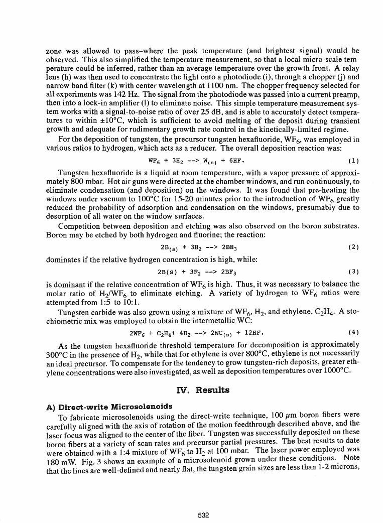
carefully aligned with the axis of rotation of the motion feedthrough described a~ove, and thelaser focus was aligned to the center of the fiber. Tungsten was successfully deposited on theseboron fibers at a variety of scan rates and precursor partial pressures. The best results to datewere obtained with a 1:4 mixture of WF6 to H2 at 100 mbar. The laser power e~ployed was180 mW. Fig. 3 shows an example of a microsolenoid grown under these conditions.. Notethat the lines are well-defined and nearly flat, the tungsten grain sizes are less than microns,
532

Tungsten on Boron Microsolenoid by Laser Direct-writing
and there little deposition of tungsten or etching of boron between the lines. Average centralthickness was 3 }lm.
The thickness of the tungsten lines was found to be inversely proportional to the scan rate,while the width of the lines was approximately the same as the spot size (10-15 }lm) over awide range of scan rates, but broadened as the scan rate approached zero velocity, reducing theresolution of the helix and number of possible turns per unit length. In addition, it was notedthat increasing overall pressure tended to increase the deposition rate and reduce the grain sizeof the tungsten deposit. So, to maintain consistent results and high definition lines, the scanrate had to be raised as the pressure was increased.
addition to the boron-core microsolenoids, tungsten was also deposited on 100 }lm diameter alloy fibers. To insulate the core from the tungsten coil, the fibers wereCVD-coated with a }lm thick silicon layer using a silane and hydrogen ambient and resistive heating of the Co-alloy fibers. The adhesion of the silicon coating to the Co-alloy fiberswas adequate. Tungsten could be readily grown on these fibers, as in the case of the boroncore microsolenoids, although higher laser powers, on the order of 500 mW, were required tocompensate for the thermal conductivity of Co-alloy, and the Si coating was readilyetched, leaving the metal lines uninsulated. Ongoing efforts are being made to substitute aboron coating for silicon, so that these microelectromagnets may be fully tested.
rele-~;ta,nClin~g Microsolenoidsa basis comparison and because of its outstanding mechanical properties and favor-
able microstructure, carbon was selected as the preliminary deposit material for growing freestanding microcoils, since the 3D-LCVD of amorphous carbon rods from ethylene has beenpreviously characterized.6 As described earlier, functional microsolenoids could also be fabricated using the carbon helices as cores, or carbon could be used as a sacrificial layer in theproduction of microtubes.
Again, boron fibers were used as the substrates, aligned to the rotary feedthrough axis. Ethylene was introduced at pressures between 400 and 3000 mbar, and laser powers between150 mW 1200 mW provided a variety of carbon fiber diameters. At 930 mbar and
mW, smooth, amorphous carbon fibers could be grown with a diameter of only 14 }lm.
Using as a basis, several dozen helices were grown, one of which is displayedindividual coils could be spaced less than 5 }lm apart without affecting
533


the "' .........JljOi, ...." .............. U....,IJV':;IJlLL>
(EDS). No traceratios as low as
535

Freeform Growth of we HelicesTo obtain conductive, freestanding helices, experiments were also performed in the growth
of tungsten carbide from a stochiometric mix of WF6' CZH4, and Hz. Again, very rapid continuous growth was obtained, up to 175 Jtrrtls, while the diameter of the fibers was much smallerthan that of the pure tungsten samples-as narrow as 20 pm across. Focal tracking wasemployed to grow fibers as long as 4 mm, with height-to-width aspect ratios of 200: 1. Thefibers tended to grow in spurts, as hexagonal single-crystals with peak growth rates exceeding200 pmJs in many instances. Single-crystal deposition rates were so rapid that they were difficult to measure. To obtain polycrystalline deposits, a chopper at 72 Hz was introduced, andsmooth, continuous growth at 10-20 pmJs was obtained. In this way, it was possible to changethe axial direction of the growth, allowing helices of WC to be prototyped, such as that shownin Fig. 5B. This helix was grown with a 1:2:2 ratio of WF6:CzH4:Hzat 765 mbar.
Morphology of the tungsten carbide deposits depended strongly on the laser poweremployed. At the highest powers, several different phases of the W-C system were present,while at low powers, bare hexagonal crystals of WC were obtained. X-ray diffraction studiesare currently underway to identify all of the phases. A thin, pure tungsten coating was presenton the exterior of many WC structures, due to the differential in threshold decomposition temperatures between WF6 and CZH4• This coating may be readily delaminated, and can be eliminated through the use of low powers, pulsed lasers, or alternate precursors for carbon.
V. ConclusionsBoth direct-write and free-standing microsolenoids and electromagnets may be fabricated
using 3D-LCVD. Future work will include the incorporation of ferromagnetic materials, thetesting and characterization of the resulting microelectromagnets, and their application inmicroelectromechanical systems (MEMS). Additional studies will be carried out on the effectsof noble gases on heat losses during 3D-LCVD, and the deposition of tungsten andtungsten carbide systems will be fully characterized.
VI. Bibliography1. 1.A. Rodgers, R. J. Jackman, G. M. Whitesides, "Constructing Single- and Multiple- Helical Microcoils and Char
acterizing Their Performance as Components of Microinductors and Microelectrornagnets," Journal of Microelectromechanical Systems, Vol. 6, No.3, Sept. 1997, pp. 184-191.
Z. J. Klein, H. Guckel, "High Winding Density Micro Coils for Magnetic Actuators," HARMST '97, Madison, WI,Jun. 1997.
3. H. Westberg, M. Boman, "Free-standing Silicon Microstructures Fabricated by Laser Chemical Processing,"J. Appl. Physics, Vol. 73, No. 11, 1 Jun. 1993, pp. 7864-7871.
4. Maxwell, J., Pegna, J., DeAngelis, D., Messia, D., "Three-dimensional Laser Chemical Vapor Deposition of Nickel-Iron Alloys," Material Research Society Symposium Proceedings, v. 397 (B3.30): Advanced Laser Processing,MRS Fall 1995 Meeting, Boston, MA (Nov. 27--Dec.l, 1995).
5. S. Johansson, J. Schweitz, H. Westberg, M. Boman, "Microfabrication of Three-Dimensional Boron Structuresby Laser Chemical Processing," 1. A~~l. Phys., Vol. 72, No. 12, 15 Dec. 1992, pp. 5956-5963.
6. J. Maxwell, "Three-Dimensional Laser-Induced Pyrolysis: Modelling, Growth Rate Control, and Application toMicro-Scale Prototyping," PhD Thesis, Rensselaer Polytechnic Institute, 1996.
7. P. Lorrain, D. Corson, Electromagnetic Fields and Waves, 2nd Edition, Freeman Pub!. San Francisco, CA, 1970,
pp.398.
8. Maxwell J., Krishnan, K., "High-Pressure, Convectively-Enhanced, Laser Chemical Vapor Deposition of Titaniurn," Proc. Solid Freeform Fabrication Symposium, Austin, Texas, Aug. 1997.
536