real time testing and validation of a novel short circuit
TRANSCRIPT

Western University Western University
Scholarship@Western Scholarship@Western
Electronic Thesis and Dissertation Repository
8-20-2015 12:00 AM
Real Time Testing and Validation of a Novel Short Circuit Current Real Time Testing and Validation of a Novel Short Circuit Current
(SCC) Controller for a Photovoltaic Inverter (SCC) Controller for a Photovoltaic Inverter
Vishwajitsinh H. Atodaria, The University of Western Ontario
Supervisor: Dr. Rajiv K. Varma, The University of Western Ontario
A thesis submitted in partial fulfillment of the requirements for the Master of Engineering
Science degree in Electrical and Computer Engineering
© Vishwajitsinh H. Atodaria 2015
Follow this and additional works at: https://ir.lib.uwo.ca/etd
Part of the Power and Energy Commons
Recommended Citation Recommended Citation Atodaria, Vishwajitsinh H., "Real Time Testing and Validation of a Novel Short Circuit Current (SCC) Controller for a Photovoltaic Inverter" (2015). Electronic Thesis and Dissertation Repository. 3166. https://ir.lib.uwo.ca/etd/3166
This Dissertation/Thesis is brought to you for free and open access by Scholarship@Western. It has been accepted for inclusion in Electronic Thesis and Dissertation Repository by an authorized administrator of Scholarship@Western. For more information, please contact [email protected].

REAL TIME TESTING AND VALIDATION OF A NOVEL SHORT CIRCUIT CURRENT (SCC) CONTROLLER FOR A PHOTOVOLTAIC INVERTER
(Thesis format: Monograph)
by
Vishwajitsinh Atodaria
Graduate Program in Electrical and Computer Engineering
A thesis submitted in partial fulfillment of the requirements for the degree of
Master of Engineering Science
The School of Graduate and Postdoctoral Studies The University of Western Ontario
London, Ontario, Canada
© Vishwajitsinh Atodaria 2015

ii
Abstract
About 45% applications from PV solar farm developers seeking connections to the
distribution grids in Ontario were denied in 2011-13 as the short circuit current (SCC)
capacity of several distribution substations had already been reached. PV solar system
inverters typically contribute 1.2 p.u. to 1.8 p.u. fault current which was not considered
acceptable by utility companies due to the need for very expensive protective breaker
upgrades. Since then, this cause has become a major impediment in the growth of PV based
renewable systems in Ontario.
A novel predictive technique has been patented in our research group for management of
short circuit current contribution from PV inverters to ensure effective deployment of solar
farms. This thesis deals with the real time testing and validation of a short circuit current
(SCC) controller based on the above technique. With this SCC controller, the PV inverter
can be shut off within 1-2 milliseconds from the initiation of any fault in the grid that can
cause the short circuit current to exceed the rated current of the inverter. Therefore, the
power system does not see any short circuit current contribution from the PV inverter and
no expensive upgrades in protective breakers are required in the system.
The performance of the PV solar system with the short circuit current controller is
simulated and tested using (i) industry grade electromagnetic transients software
PSCAD/EMTDC (ii) real time simulation studies on the Real Time Digital Simulator
(RTDS) (iii) physical implementation on dSPACE board to generate firing pulses for the
inverter. The validation of controller is done on dSPACE board with actual PV inverter
short circuit waveforms obtained from Southern California Edison Short Circuit Testing
Lab. This novel technology is planned to be showcased on a physical 10 kW PV solar
system in Bluewater Power Distribution Corporation, Sarnia, Ontario. This proposed
technology is expected to remove the technical hurdles which caused the denials of
connectivity to several PV solar farms, and effectively lead to greater connections of PV
solar farms in Ontario and in similar jurisdictions, worldwide.

iii
Keywords
Renewable Energy, Solar System, Photovoltaic Power System, Protection, Inverter,
Predictive Control, Short Circuit Current, Real Time Digital Simulation, Distributed
Generator.

iv
Dedicated to my
Family and Friends

v
Acknowledgments
I would like to express my sincere gratitude to my supervisor, Dr. Rajiv K. Varma, for his
generous support, valuable suggestions, and constructive guidelines in every step of my
graduate career at Western University. I feel very proud to have had the opportunity to
work under his kind supervision and to have the opportunity to work within industry that
has enriched my knowledge and built my confidence to succeed in my future career. No
words are adequate to express my gratefulness to him. I, herewith, convey my sincere and
warmest regards to him.
I am highly obliged to Tim Vanderheide, Chief Operating Officer, Bluewater Power
(BWP) Corporation to have provided me the rare opportunity to work closely with
industrial people. I convey my profound respect to him as well. I would also like to thank
Maureen Glaab, Energy Services Coordinator, BWP, for her very co-operative and friendly
manner which made my working environment much more informal.
I would like to gratefully acknowledge Mr. Richard J. Bravo and Mr. Steven Robles for
providing actual short circuit results for commercial inverters from Southern California
Edison Short Circuit Testing Lab. I am also thankful to Dr. Vijay Parsa for the valuable
discussions and suggestions in the initial part of this project.
I also acknowledge the Ontario Centres of Excellence (OCE), Hydro One Networks Inc.,
Bluewater Power Corp., and Natural Sciences and Engineering Research Council
(NSERC) for their financial support for two years.
I am deeply thankful to all my friends Sibin, Diwash, Sridhar, Ehsan, Hesam, Mohammed,
and Reza for their constant encouragement and support during my stay at Western
University.
I would like to express my affectionate appreciation to my family for their unwavering
faith and continuous encouragement to work hard during my academic education. It would
not have been possible without their love.
VISHWAJITSINH ATODARIA

vi
Table of Contents
Abstract ............................................................................................................................... ii
Acknowledgments............................................................................................................... v
Table of Contents ............................................................................................................... vi
List of Tables ..................................................................................................................... xi
List of Figures ................................................................................................................... xii
List of Appendices .......................................................................................................... xvii
List of Abbreviations ..................................................................................................... xviii
List of Symbols ................................................................................................................. xx
CHAPTER 1 ....................................................................................................................... 1
INTRODUCTION .............................................................................................................. 1
1.1 GENERAL .............................................................................................................. 1
1.2 PV INVERTER MODELING ................................................................................ 2
1.2.1 PV Inverter Configuration .......................................................................... 2
1.2.2 Control Schemes for PV Inverter ................................................................ 4
1.2.3 Inverter Firing Strategy ............................................................................... 4
1.3 SHORT CIRCUIT CURRENT CONTRIBUTION OF GRID CONNECTED
PV SOLAR SYSTEM............................................................................................. 4
1.4 CONDITIONS FOR DISCONNECTING PV INVERTER ................................... 5
1.5 FAULT DETECTION TECHNIQUES .................................................................. 6
1.6 SIMULATION STUDIES ...................................................................................... 8
1.6.1 Electromagnetic Transients Software Simulation Studies .......................... 9
1.6.2 Real Time Digital Simulation Studies ........................................................ 9

vii
1.6.3 Implementation on Digital Controller Board ............................................ 10
1.7 MOTIVATION OF THESIS ................................................................................ 10
1.8 OBJECTIVE AND SCOPE OF THESIS ............................................................. 11
1.9 OUTLINE OF THESIS......................................................................................... 12
CHAPTER 2 ..................................................................................................................... 14
MODELING OF THREE PHASE GRID CONNECTED PHOTOVOLTAIC SYSTEM
WITH SHORT CIRCUIT CURRENT CONTROLLER ............................................. 14
2.1 INTRODUCTION ................................................................................................ 14
2.2 SYSTEM MODEL................................................................................................ 15
2.2.1 System Description ................................................................................... 15
2.2.2 PV Source Model ...................................................................................... 17
2.2.3 Inverter Control Modeling ........................................................................ 17
2.2.4 DC Link Capacitor .................................................................................... 27
2.2.5 LCL Filter Modeling and Design .............................................................. 29
2.2.6 Step Up Transformer................................................................................. 31
2.3 SHORT CIRCUIT CURRENT CONTROLLER DESIGN .................................. 32
2.3.1 Concept ..................................................................................................... 32
2.3.2 Short Circuit Current Controller Module .................................................. 32
2.3.3 Performance of Short Circuit Current Controller Module ........................ 37
2.4 CONCLUSION ..................................................................................................... 41
CHAPTER 3 ..................................................................................................................... 42
ELECTROMAGNETIC TRANSIENTS SIMULATION USING PSCAD
SOFTWARE ................................................................................................................ 42
3.1 INTRODUCTION ................................................................................................ 42
3.2 SYSTEM MODEL................................................................................................ 42
3.3 IMPLEMENTATION OF SCC CONTROLLER IN PSCAD SOFTWARE ....... 44

viii
3.4 ASYMMETRICAL FAULT STUDIES ............................................................... 48
3.4.1 Single Line - Ground Fault ....................................................................... 48
3.4.2 Line - Line Fault ....................................................................................... 51
3.4.3 Line - Line - Ground Fault ........................................................................ 55
3.5 SYMMETRICAL FAULT STUDIES .................................................................. 55
3.5.1 Line - Line - Line Fault ............................................................................. 55
3.5.2 Line - Line - Line Ground Fault ............................................................... 59
3.6 FAULT STUDIES AT DIFFERENT TIME INSTANTS .................................... 59
3.6.1 Asymmetrical Fault ................................................................................... 59
3.6.2 Symmetrical Fault ..................................................................................... 63
3.7 RESPONSE TIME OF SCC CONTROLLER FOR FAULTS AT DIFFERENT
TIME INSTANTS ................................................................................................ 67
3.8 LOAD SWITCHING ............................................................................................ 68
3.9 CONCLUSION ..................................................................................................... 69
CHAPTER 4 ..................................................................................................................... 71
REAL TIME SIMULATION USING REAL TIME DIGITAL SIMULATOR (RTDS)
...................................................................................................................................... 71
4.1 INTRODUCTION ................................................................................................ 71
4.2 OVERVIEW OF REAL TIME DIGITAL SIMULATOR ................................... 71
4.2.1 Concept ..................................................................................................... 71
4.2.2 Hardware Structure ................................................................................... 72
4.3 SYSTEM MODEL................................................................................................ 75
4.4 IMPLEMENTATION OF SCC CONTROLLER IN RTDS ................................ 75
4.5 ASYMMETRICAL FAULT STUDIES ............................................................... 77
4.5.1 Single Line - Ground Fault ....................................................................... 77
4.5.2 Line - Line Fault ....................................................................................... 81

ix
4.5.3 Line - Line - Ground Fault ........................................................................ 84
4.6 SYMMETRICAL FAULT STUDIES .................................................................. 85
4.6.1 Line - Line - Line Fault ............................................................................. 85
4.6.2 Line - Line - Line - Ground Fault ............................................................. 89
4.7 FAULT STUDIES AT DIFFERENT TIME INSTANTS .................................... 92
4.7.1 Asymmetrical Fault ................................................................................... 92
4.7.2 Symmetrical Fault ..................................................................................... 96
4.8 LOAD SWITCHING .......................................................................................... 100
4.9 COMPARISON BETWEEN RTDS AND PSCAD RESULTS ......................... 101
4.10 CONCLUSION ................................................................................................... 102
CHAPTER 5 ................................................................................................................... 104
VALIDATION OF SHORT CIRCUIT CURRENT CONTROLLER ON dSPACE ..... 104
5.1 INTRODUCTION .............................................................................................. 104
5.2 CONCEPT OF dSPACE SIMULATION ........................................................... 104
5.3 OVERVIEW OF dSPACE PLATFORM ........................................................... 105
5.3.1 dSPACE Software ................................................................................... 105
5.3.2 dSPACE Controller Board ...................................................................... 106
5.4 ANALYSIS OF ACTUAL SHORT CIRCUIT CURRENT WAVEFORMS .... 107
5.4.1 Single - Line Ground Fault ..................................................................... 108
5.4.2 Line - Line Fault ..................................................................................... 110
5.4.3 Line - Line - Ground Fault ...................................................................... 112
5.5 IMPLEMENTATION OF SCC CONTROLLER ON dSPACE BOARD ......... 114
5.6 dSPACE RESULTS ............................................................................................ 117
5.6.1 Single Line - Ground Fault ..................................................................... 118
5.6.2 Line - Line Fault ..................................................................................... 121

x
5.6.3 Line - Line - Ground Fault ...................................................................... 124
5.7 COMPARISON BETWEEN dSPACE AND RTDS RESULTS........................ 127
5.8 ACTUAL IMPLEMENTATION OF SCC CONTROLLER ............................. 127
5.8.1 TMS320F28335 eZdsp Board................................................................. 128
5.8.2 Current Sensor ........................................................................................ 129
5.8.3 DC Switch ............................................................................................... 130
5.8.4 AC Switch ............................................................................................... 130
5.8.5 Interfacing Circuits ................................................................................. 131
5.8.6 Hardware Implementation of the Short Circuit Current Controller ........ 134
5.8.7 Customization ......................................................................................... 134
5.9 CONCLUSION ................................................................................................... 135
CHAPTER 6 ................................................................................................................... 137
CONCLUSIONS AND FUTURE WORK ..................................................................... 137
6.1 INTRODUCTION .............................................................................................. 137
6.2 A NOVEL SHORT CIRCUIT CURRENT CONTROLLER FOR PV SOLAR
SYSTEM ............................................................................................................. 138
6.3 ELECTROMAGNETIC TRANSIENT SIMULATION USING PSCAD
SOFTWARE ....................................................................................................... 138
6.4 REAL TIME SIMULATION USING RTDS ..................................................... 139
6.5 VALIDATION OF SHORT CIRCUIT CURRENT CONTROLLER ON
dSPACE .............................................................................................................. 140
6.6 THESIS CONTIBUTIONS ................................................................................ 141
6.7 PUBLICATIONS ................................................................................................ 142
6.8 FUTURE WORK ................................................................................................ 142
REFERENCES ............................................................................................................... 143
APPENDIX: System Data .............................................................................................. 152

xi
List of Tables
Table 1.1: Voltage Range and Maximum Clearing Time ....................................................5
Table 1.2: Frequency Range and Maximum Clearing Time ...............................................6
Table 3.1: Response Time of SCC Controller during LL Fault ........................................67
Table 3.2: Response Time of SCC Controller during LLL Fault .....................................67
Table 5.1: Oscillation Frequencies of the Inverter Current during SLG Fault ................109
Table 5.2: Oscillation Frequencies of the Inverter Current during LL Fault ...................111
Table 5.3: Oscillation Frequencies of the Inverter Current during LLG Fault ................113
xii
List of Figures
Figure 1.1: Cumulative installed PV capacity 2000-2013 .................................................. 1
Figure 1.2: Typical PV solar farm inverter ......................................................................... 3
Figure 2.1: Single Line Diagram of System Model .......................................................... 15
Figure 2.2: Detailed PV System Inverter and Conventional Controller with Incorporated
Short Circuit Current Controller ....................................................................................... 16
Figure 2.3: General VSI based PV Inverter Controller..................................................... 18
Figure 2.4: Vector Representation of Three Phase Electrical Variables in Stationary (abc)
and Rotating Reference (dq) Frame .................................................................................. 20
Figure 2.5: Schematic Diagram of PV Inverter Connected to Grid .................................. 21
Figure 2.6: Block Diagram of Inner Loop VSI Current Controller .................................. 26
Figure 2.7: Sinusoidal Pulse Width Modulation Technique for VSI ............................... 27
Figure 2.8: Block Diagram of SCC Controller Module .................................................... 33
Figure 2.9: Flow Chart of SCC Controller........................................................................ 36
Figure 2.10: Inverter Output Current for SLG Fault (a) Phase A (b) Phase B ................. 38
Figure 2.11: Inverter Output Current for LL Fault (a) Phase A (b) Phase B .................... 39
Figure 2.12: Inverter Output Current for LLG Fault (a) Phase A (b) Phase B ................. 40
Figure 3.1: System Model with PV System Inverter, Conventional Controller and the
incorporated Short Circuit Current Controller in PSCAD/EMTDC ................................. 43
Figure 3.2: Implementation of SCC Controller in PSCAD .............................................. 44

xiii
Figure 3.3: (a) Inverter Fault Current at t = 2 sec. (b) Triggering Signals (c) Inverter Fault
Current with SCC Controller ............................................................................................ 49
Figure 3.4: Zoomed Waveforms of (a) Inverter Fault Current at t = 2 sec. (b) Triggering
Signals (c) Inverter Fault Current with SCC Controller ................................................... 50
Figure 3.5: (a) Inverter Fault Current at t = 2 sec. (b) Triggering Signals (c) Inverter Fault
Current with SCC Controller ............................................................................................ 53
Figure 3.6: Zoomed Waveforms of (a) Inverter Fault Current at t = 2 sec. (b) Triggering
Signals (c) Inverter Fault Current with SCC Controller ................................................... 54
Figure 3.7: (a) Inverter Fault Current at t = 2 sec. (b) Triggering Signals (c) Inverter Fault
Current with SCC Controller ............................................................................................ 57
Figure 3.8: Zoomed Waveforms of (a) Inverter Fault Current at t = 2 sec. (b) Triggering
Signals (c) Inverter Fault Current with SCC Controller ................................................... 58
Figure 3.9: (a) Inverter Fault Current at t = 4.5 sec. (b) Triggering Signals (c) Inverter Fault
Current with SCC Controller ............................................................................................ 61
Figure 3.10: Zoomed Waveforms of (a) Inverter Fault Current at t = 4.5 sec. (b) Triggering
Signals (c) Inverter Fault Current with SCC Controller ................................................... 62
Figure 3.11: (a) Inverter Fault Current at t = 5 sec. (b) Triggering Signals (c) Inverter Fault
Current with SCC Controller ............................................................................................ 65
Figure 3.12: Zoomed Waveforms of (a) Inverter Fault Current at t = 5 sec. (b) Triggering
Signals (c) Inverter Fault Current with SCC Controller ................................................... 66
Figure 3.13: (a) PV Inverter Current with 60 MW, 0.9 pf Load Switching (b) Triggering
Signals from SCC Controller ............................................................................................ 69
Figure 4.1: RTDS Hardware ............................................................................................. 74
Figure 4.2: Implementation of SCC Controller in RSCAD .............................................. 76

xiv
Figure 4.3: D Flip-Flop ..................................................................................................... 76
Figure 4.4: (a) Inverter Fault Current at t = 2 sec. (b) Triggering Signals (c) Inverter Fault
Current with SCC Controller ............................................................................................ 78
Figure 4.5: Zoomed Waveforms of (a) Inverter Fault Current at t = 2 sec. (b) Triggering
Signals (c) Inverter Fault Current with SCC Controller ................................................... 80
Figure 4.6: (a) Inverter Fault Current at t = 2 sec. (b) Triggering Signals (c) Inverter Fault
Current with SCC Controller ............................................................................................ 82
Figure 4.7: Zoomed Waveforms of (a) Inverter Fault Current at t = 2 sec. (b) Triggering
Signals (c) Inverter Fault Current with SCC Controller ................................................... 84
Figure 4.8: (a) Inverter Fault Current at t = 2 sec. (b) Triggering Signals (c) Inverter Fault
Current with SCC Controller ............................................................................................ 86
Figure 4.9: Zoomed Waveforms of (a) Inverter Fault Current at t = 2 sec. (b) Triggering
Signals (c) Inverter Fault Current with SCC Controller ................................................... 88
Figure 4.10: (a) Inverter Fault Current at t = 2 sec. (b) Triggering Signals (c) Inverter Fault
Current with SCC Controller ............................................................................................ 90
Figure 4.11: Zoomed Waveforms of (a) Inverter Fault Current at t = 2 sec. (b) Triggering
Signals (c) Inverter Fault Current with SCC Controller ................................................... 91
Figure 4.12: (a) Inverter Fault Current at t = 5.0018 sec. (b) Triggering Signals (c) Inverter
Fault Current with SCC Controller ................................................................................... 94
Figure 4.13: Zoomed Waveforms of (a) Inverter Fault Current at t = 5.0018 sec. (b)
Triggering Signals (c) Inverter Fault Current with SCC Controller ................................. 95
Figure 4.14: (a) Inverter Fault Current at t = 3.5077 sec. (b) Triggering Signals (c) Inverter
Fault Current with SCC Controller ................................................................................... 98

xv
Figure 4.15: Zoomed Waveforms of (a) Inverter Fault Current at t = 3.5077 sec. (b)
Triggering Signals (c) Inverter Fault Current with SCC Controller ................................. 99
Figure 4.16: (a) PV Inverter Current with 60 MW, 0.9 pf. Load Switching (b) Triggering
Signals from SCC Controller .......................................................................................... 101
Figure 5.1: Block Diagram of dSPACE Software System ............................................. 105
Figure 5.2: Block Diagram of dSPACE Hardware System ............................................ 106
Figure 5.3: FFT of Inverter Fault Current during SLG Fault ......................................... 108
Figure 5.4: FFT of Inverter Fault Current during LL Fault ............................................ 110
Figure 5.5: FFT of Inverter Fault Current during LLG Fault ......................................... 112
Figure 5.6: Implementation of SCC Controller on dSPACE .......................................... 115
Figure 5.7: Filter Delay ................................................................................................... 116
Figure 5.8: dSPACE Test Set Up .................................................................................... 117
Figure 5.9: (a) Inverter Fault Current (b) Filtered Inverter Fault Current (c) Triggering
Signal and (d) Inverter Fault Current with SCC Controller ............................................ 119
Figure 5.10: Performance of SCC Controller in Yokogawa during SLG Fault.............. 120
Figure 5.11: (a) Inverter Fault Current (b) Filtered Inverter Fault Current (c) Triggering
Signal and (d) Inverter Fault Current with SCC Controller ............................................ 122
Figure 5.12: Performance of SCC Controller in Yokogawa during LL Fault ................ 123
Figure 5.13: (a) Inverter Fault Current (b) Filtered Inverter Fault Current (c) Triggering
Signal and (d) Inverter Fault Current with SCC Controller ............................................ 125
Figure 5.14: Performance of SCC Controller in Yokogawa during LLG Fault ............. 126
Figure 5.15: Implementation of SCC Controller on a 10 kW PV Solar System ............ 128
xvi
Figure 5.16: TMS320F28335 eZdsp Board .................................................................... 129
Figure 5.17: Current Sensor LA 55-P ............................................................................. 130
Figure 5.18: DC Switch .................................................................................................. 131
Figure 5.19: AC Switch .................................................................................................. 131
Figure 5.20: Interfacing between Current Sensor and TMS320F28335 eZdsp Board ... 132
Figure 5.21: Interfacing between TMS320F28335 eZdsp Board and Gating Signals .... 133
Figure 5.22: Interfacing Circuit between TMS320F28335 eZdsp Board and DC Switch
......................................................................................................................................... 134
Figure 5.23 : Hardware of the Short Circuit Current Controller..................................... 135

xvii
List of Appendices
APPENDIX: System Data ...............................................................................................152

xviii
List of Abbreviations
AC Alternating Current
DC Direct Current
DG Distributed Generation
DDAC Digital to Digital Analog Converter
DSP Digital Signal Processor
EMTDC Electromagnetic Transient including DC
EMTP Electromagnetic Transient Program
FACTS Flexible AC Transmission System
FCL Fault Current Limiter
Fortan Formula Translation
GTDI Gate Transceiver Digital Input
GTO Gate Turn Off Thyristor
HIL Hardware-in-the-Loop
HV High Voltage (winding)
IEEE Institute of Electrical & Electronics Engineers
IGBT Insulated Gate Bipolar Transistor
IIR Infinite Impulse Response
LV Low Voltage (winding)
LVRT Low Voltage Ride Through
LL Line to Line Fault
LLG Line to Line to Ground Fault
LLL Line to Line to Line Fault
LLLG Line to Line to Line to Ground Fault
MPPT Maximum Power Point Tracking

xix
ON Ontario
PCC Point of Common Coupling
PI Proportional Integral
PLL Phase Locked Loop
PSCAD Power System Computer Aided Design
p.u. per unit
PV Photovoltaic
PWM Pulse Width Modulation
RMS Root Mean Square
SCC Short Circuit Current
SCE Southern California Edison
SLG Single Line to Ground Fault
SPICE Simulation Program with Integrated Circuit Emphasis
SPWM Sinusoidal Pulse Width Modulation
STC Standard Test Condition
TDD Total Demand Distortion
THD Total Harmonic Distortion
VAr Reactive Volt Ampere
VSC Voltage Source Converter
VSI Voltage Source Inverter

xx
List of Symbols
θ Instantaneous angle between a-axis and d-axis
Ω Grid frequency (377 rad/s)
∆ Transformer winding configuration (delta)
Ω Ohm unit
µ Micro unit
𝜏 Time constant
m Millisecond

1
CHAPTER 1
INTRODUCTION
1.1 GENERAL
Renewable energy sources are being increasingly implemented worldwide for
environmental considerations. Solar energy is the most widely available source of
nonpolluting energy. Although photovoltaic (PV) technology (converts sunlight into
electricity) is expensive, it is receiving strong encouragement through various global
incentives programs [1,2]. An unprecedented growth of photovoltaic system has been seen
over the past few years both in Canada and worldwide. On a global scale, approximately
39,000 MW of new PV were added during 2013, raising the total installed capacity to 138.9
GW [3]. Figure 1.1 shows the evolution of a global PV installation capacity from 2000 to
2013.
Figure 1.1: Cumulative installed PV capacity 2000-2013 [3]

2
Integration of more Distributed Generators (DGs) in the power system network presents
several challenges such as voltage variations, reverse power flows and increase in the short
circuit current contribution of the DGs during faults [4,5]. Hence, utility companies,
especially in Ontario, Canada, are limiting the connections of DGs into their networks
where the short circuit current capacity limits has already been reached [6]. This is done
due to the apprehension that short circuit current contribution from DGs may overload the
breaker equipment and necessitate expensive breaker protective upgrades [6,7]. A novel
technique has been developed and patented for management of short circuit contribution
from PV inverters [8,9]. This thesis deals with the comprehensive testing of a short circuit
current (SCC) controller based on the above technique through Real Time Digital
Simulation (RTDS), dSPACE simulation and validation with actual short circuit current
signals obtained from the Southern California Edison (SCE) Short Circuit Testing Lab. The
developed SCC controller disconnects the PV inverter from the grid within 1-2
milliseconds from the initiation of any fault in the grid that is likely to cause the short
circuit current to exceed the rated inverter current. With this technique, the power system
does not experience any short circuit current contribution from the PV inverter and hence
the electrical system is protected from any potential damage caused by high magnitude of
fault currents.
1.2 PV INVERTER MODELING
1.2.1 PV Inverter Configuration
In PV power plants, there are a number of PV arrays connected to the power converter
depending on the size of PV inverters. PV systems of low power level i.e., less than 10 kW
are usually configured with a single phase inverter or three phase inverter. However, PV
solar systems in the power range of 10 kW to 100 kW are configured with a three phase
inverter at a line voltage of 480 V [12]. The output voltage of the PV inverters is
transformed to a higher voltage internally or externally to the inverter through step-up
transformers [12].
There are two types of inverter configurations employed presently in solar farms. They are
string inverters and micro inverters. In string inverter technology, several modules in string

3
configuration are fed into a single large inverter and are grouped together to feed into a
large grid [13,14]. Micro-inverter is also known as AC module technology. Each module
has its own inverter and the output of all micro-inverters are integrated together to feed the
grid [15,16].
Numerous inverter topologies have been employed for grid connected PV solar farms.
They are single state topology for single modules [17], two state topology for multiple
modules [18], multilevel inverter topology [19,20], fly-back type inverter [21], fly-back
current fed inverter [22] and resonant inverter [23]. Performance of different topologies
used by several commercial manufacturers are compared in review of PV modules [24,25].
To construct inverter circuits, manufacturers use Metal-Oxide Semiconductor Field Effect
Transistor (MOSFET), Gate Turn-Off (GTO) thyristor, and Insulated Gate Bipolar
Transistor (IGBT) switches [26]. Mostly manufacturers use IGBT switches because of their
low loss and ease of switching [26,27]. A typical solar farm inverter is a six pulse inverter
comprised of 6 IGBT switches as shown in Figure 1.2 [28], with associated snubber circuits
for smooth switching operations. The firing pulses to trigger the IGBT switches are
generated from the inverter controller.
gt1
gt4
gt3
gt6
gt5
gt2
Vdc
A
B
C
CdcAC Filter
PCC Coupling Transformer
PV Inverter Controller
Voltage Source Inverter
PV
Mo
du
le o
r D
C-D
C
Co
nve
rte
rIGBT
Figure 1.2: Typical PV solar farm inverter

4
1.2.2 Control Schemes for PV Inverter
Typically, the controller of a PV solar system is a combination of two control loops: Outer
and Inner Control Loop. The outer control loop can be of different types depending upon
the operational objectives from the PV system [29,30]. This loop can be used for
controlling real and reactive power, AC voltage, DC voltage, etc. The reference currents
are generated by the outer control loop. The inner control loop tracks these reference
currents. This loop is a current control loop, generating signals for the switching pulse
generation module to generate firing pulses for the inverter switches.
1.2.3 Inverter Firing Strategy
Various techniques are used to generate firing pulses for the IGBTs in the inverter such as
Sinusoidal Pulse Width Modulation (SPWM), Sinusoidal Vector Pulse Width Modulation
(SVPWM) and Hysteresis control [31,32]. Among all these techniques, the SPWM
technique is widely used for high power PV inverter applications [31]. In SPWM [32],
generation of desired output voltage is achieved by comparing the desired reference
waveform with a high frequency triangular carrier wave.
1.3 SHORT CIRCUIT CURRENT CONTRIBUTION OF GRID CONNECTED PV SOLAR SYSTEM
About 45% applications from PV solar farm developers seeking connections to the
distribution grids in Ontario were denied during the period 2011-13 as the short circuit
current capacity of the substations was already reached [33]. The short circuit current
contribution from a PV system inverter is in the range of 1.2 times the rated current for the
large size inverter (1MW), 1.5 times for the medium size inverter (500kW) and 2 - 3 times
for the smaller inverters [32,33]. Further this short circuit current contribution continues
for a period ranging from 4 to 10 cycles [31,34]. Although this amount of short circuit
current is small for each PV solar system, the total amount of fault contribution becomes
unacceptably large for a distribution line that has a large number of PV systems [33,35].
This was not considered acceptable by utility companies due to the need of very expensive
upgrades of protective breakers [31]. This has resulted into the substantial loss of

5
opportunity to integrate more PV based renewable generation at least in the Ontario
network.
1.4 CONDITIONS FOR DISCONNECTING PV INVERTER
According to several grid interconnection standards [38,39,40], regardless of fault level, it
is required to disconnect the PV solar farms or any other DGs upon detection of fault on
the system. Therefore, it is not only important to detect the faults rapidly, but also to
disconnect the DGs from the network as quickly as possible. IEEE Standard 1547
standardizes the rules for connecting distributed generation including PV inverters to the
distribution network. This Standard is intended to ensure that Distributed Generators do
not violate some of the basic rules of the distribution system for safe and reliable operation
of an electrical system. PV inverter manufacturers strive to comply with IEEE 1547 [38],
implement anti-islanding operation and ensure that PV inverters stay connected within
allowable voltage time and frequency time operating region [12]. Table 1 lists the operating
voltage and maximum clearing time and Table 2 lists the operating frequency and
maximum clearing time for distributed generation as specified in IEEE 1547 [38].
Voltage Range
(% Nominal)
*Max. Clearing Time
(seconds)
V < 50% 0.16
50% < V < 88% 2
V > 120% 0.16
110% < V < 120% 1
(*) For DER ≤ 30 kW; default clearing times for DER > 30 kW
Table 1.1: Voltage Range and Maximum Clearing Time [12]

6
Frequency Range
(Hz)
Max. Clearing Time
(seconds)
f > 60.5 0.16
* f < 57.0 0.16
** 57.0 < f < 59.8 0.16 - 300
(*) 59.3 Hz if DER ≤ 30 kW; (**) for DER > 30 kW
Table 1.2: Frequency Range and Maximum Clearing Time [12]
There are also additional disconnection requirements included in IEEE 1547 [12]:
Detect island condition and cease to energize within 2 seconds of the formation of
an island, which is known as anti-islanding.
Cease to energize for faults on the area of electrical power system (EPS) circuit.
Cease to energize prior to circuit reclosure.
1.5 FAULT DETECTION TECHNIQUES
During a short circuit fault in the grid, the fault current from the PV inverter can potentially
damage the breakers and other customer equipment in the power system network.
Therefore, it is necessary to detect the faults and disconnect the DGs from the network at
a very rapid rate. This issue has not been adequately addressed in literature. Various
techniques have been developed to detect short circuit condition in PV solar system. All
these techniques are described below.
As a first step, adequate modeling of PV solar plants for predicting their short circuit
current contributions during network faults is essential [41,42]. The traditional relay
technologies mainly use overvoltage, undervoltage and overcurrent signals to detect the
faults and subsequently operate the protective breakers. A DG generating more than 1 MW
is required for transfer-trip, according to DG interconnection requirement by a utility [39].
Instantaneous over current relay used by the utility takes 17 ms to detect the fault and 5-10

7
ms to transfer the trip signal [39]. The operating time of traditional breaker is 83 ms.
Therefore, the current practice of detecting the fault and disconnecting DGs from network
through transfer trip method takes around 105-110 ms. However, by that time the short
circuit current continues to flow for 7-8 cycles and exceeds its maximum permissible limit
[39].
Grid connected inverters are required to operate at a power factor of unity [43]. However,
during the event of short circuit fault in distribution line, a larger amount of fault current
generally flows through the distribution line. Due to this, the phase angle and the absolute
value of the voltage on the distribution line changes significantly by the effect of line
impedance of distribution line at the short circuit fault [44]. A technique has been proposed
for quick detection of fault through the monitoring of change in the voltage phase angle
[45]. However, this method is not effective because in most parts of the distribution line
the voltage phase change was less than 3°. Also, it cannot detect a short circuit fault with
high fault resistance. Therefore, combined voltage phase and magnitude [44] technique
was designed for PV systems to detect short circuit fault with high fault resistance. The
drawback of this design was that it was not able to restrain the fault current completely at
substation. Also, the operation of controller during capacitor and transformer energization
effect was not taken into account.
The occurrence of grid fault can be identified by using Continuous Wavelet Transform
(CWT) [46]. The technique processes voltage and current transients for calculating the
change in supply impedance. The fault can be identified within half a cycle and decision is
made if the fault requires a DG to be disconnected. A four stage fault protection scheme
has been proposed [47] against short circuit fault for inverter based DGs. The inverter is
initially controlled as a voltage source, which changes to current controlled mode on
detection of fault, thereby limiting the inverter output current.
A protection scheme based on detecting variation in d-q components [48] of voltage
magnitude at the point of common coupling is proposed. This method depends on detecting
the oscillations in the voltage waveform which will increase the difficulty of the fault
detection. Therefore, it fails to detect all types of faults. In [49,50] the positive sequence

8
component of fundamental voltage is monitored to protect the grid against faults. There is
a time delay after the fault because of the positive sequence transformation, d-q reference
frame transformation and filter process. This affects the time to detect the fault [49]. It also
requires a complicated protection circuitry.
As per the technique reported in [12], when the voltage at any one of the phases of output
power of an inverter is less than 50%, the protective relay is set to disconnect the PV
inverter after 5 cycles. However, till 5 cycles, the PV inverter continues to contribute short
circuit current in the grid which is not acceptable.
A protection scheme based on harmonics detection during short circuit faults is proposed
in [51]. However, inverters manufactured nowadays try to keep the Total Harmonic
Distortion (THD) as low as possible. If the inverter filtering effect is good, and the
magnitude of harmonics generated is less than the threshold value, the fault can neither be
detected nor will the tripping signal be generated.
Electronically triggered fault current limiters have been used effectively to limit short
circuit currents. A concept of rate of change of current has been proposed as a minimum
fault-current change rate limit to prevent nuisance current limiter operation [52,51]. The
technique proposed in [50] contradicts with its suggestion stating rate of change of current
setting that permits tripping on symmetrical value of current, but blocks it for the same
threshold value of asymmetrical current. The technique suggested in [51] does not consider
the performance of the proposed controller during high impedance faults in the system.
So far, all the above fast fault detection techniques have been used for protection of
networks and DGs; and for asymmetrical fault detection in fault current limiters. However,
such techniques have not been used to prevent any short circuit current contribution in
excess of the rated or utility acceptable current output of PV solar inverters.
1.6 SIMULATION STUDIES
Development of new power electronic technologies needs to be analyzed comprehensively
to understand their operating characteristics and impact on power systems. The control
system is an essential part of a power electronic system which needs to be evaluated

9
thoroughly before installing it in the network. A formal procedure needs to be carried out
to transfer the simulation model to the final hardware implementation. This procedure
includes: Electromagnetic Transients Software simulation, Real-time simulation,
implementation on a digital controller board, and finally, the commissioning of the device
[54,55]. These procedures are described below.
1.6.1 Electromagnetic Transients Software Simulation Studies
The initial studies for the design of a prototype hardware model are done by using an
electromagnetic transients simulation software. This is an efficient tool for the designer to
learn about the designed power electronic system and its controller. The performance of
controller during fault or any abnormal conditions, along with steady-state operation in
power system environment can be predicted from these simulation studies. Different types
of commercial softwares are available to simulate power electronic systems such as
PSPICE [56], MATLAB/SIMULINK [57] and PSCAD/EMTDC [58], etc. PSPICE is
generally used for the simulation of low power electronic applications. Similarly,
MATLAB/SIMULNIK and PSCAD/EMTDC are employed for low and high power
electronic applications [59].
1.6.2 Real Time Digital Simulation Studies
Electromagnetic transients simulation software offers a wide range of power system
models for different type of studies. However, the main disadvantage of these tools is that
they operate in non-real time. It means that more time is taken by the software to simulate
the system phenomenon than the actual real time of the phenomena [60,61]. For instance,
a five-cycle fault may take several seconds or minutes of simulation time depending upon
the size of the system. Recent advancements in technology have enabled to simulate the
power system models in real-time [62,63]. This has become possible due to improvement
of parallel-processing computer hardware, digital signal processing and sophisticated
power system modeling techniques.
The most popular real-time digital simulation platforms available in market are RTDS and
OPAL-RT [64,65]. Real-Time Digital Simulator (RTDS) is a digital power system
simulator used widely in the application of power system controls and protection

10
equipment for performing real time and Hardware-in-the loop (HIL) simulations [66,67].
RTDS is a unique state-of-the-art simulator having multiprocessor architecture designed
specifically to simulate electrical power systems in real time [68,69]. This means that a
physical phenomenon of 1 sec. in power systems is simulated within 1 sec. of simulation
time. 44The power electronic converters having PWM carrier frequency of 5-10 kHz
require a smaller time step to validate the performance of the system. RTDS with its small
time step simulation feature has the capability to simulate power electronics controllers in
less than 2 μs [64].
1.6.3 Implementation on Digital Controller Board
The power systems network incorporated with short circuit current (SCC) controller is
simulated in real time in RTDS. Therefore, a real time hardware controller platform is
needed for a physical implementation of the SCC controller which gives real trip signals
and not simulated signals.
For rapid prototype developments, different types of real time controller platforms are used
such as dSPACE [70], National Instruments [71] and xPC targets [72]. dSPACE is a digital
controller board used extensively in several industrial applications due to its various
advantages such as visualization tools, different hardware and extensive array of software
options [73,74]. It is adopted by various industries and research centers for testing control
systems and protective relays [73,75]. The performance of the SCC controller can be
validated by testing it on dSPACE controller board. It presents an actual environment to
the control system running with real hardware, and exchanges signals in a realistic manner.
A dSPACE has a Graphical User Interface (GUI) software known as Control Desk which
is used to monitor the program variables during the run time of the simulation [70].
1.7 MOTIVATION OF THESIS
Since a significant number of applications seeking solar farm connections were denied in
Ontario, there was a substantial loss of opportunity to integrate PV based renewable
generation. Also, solar farms need to be disconnected rapidly when a fault is detected in
order to conform to technical connection requirements of the utilities. As stated in literature
search (Section 1.5), no technique has been developed so far for fast fault detection and

11
disconnection of PV solar systems. Therefore, an improved fault current management
technique is needed to ensure effective deployment of solar farms.
A novel technique has been developed and patented [10,11] according to which the PV
inverter is shut off within 1-2 milliseconds from the initiation of any fault in the grid
without the inverter current exceeding its rated peak value. The technique is based on the
rate of rise of current together with the current magnitude in a PV solar system based DG.
The power system network therefore does not see any short circuit current contribution
from the PV inverter, and no protective upgrades are required in the system. The objective
of this thesis to test, validate and implement this novel technique in Lab environment,
leading to a field demonstration of this technique.
It is emphasized that the objective of this thesis is not to detect the occurrence of any fault
in the network but only to identify such fault conditions during which the inverter current
is likely to exceed its rated magnitude. This technique is also not intended to provide Low
Voltage Ride Through (LVRT) capability to PV inverter [4].This novel technology is
expected to remove the technical hurdles which caused the denials of connectivity to PV
solar farms, and effectively lead to greater connections of PV solar farms in Ontario and
worldwide.
1.8 OBJECTIVE AND SCOPE OF THESIS
The objective and scope of the thesis are as follows:
To model and design a short circuit current (SCC) controller which disconnects a
PV solar farm from the power system network before the inverter current exceeds
its rated peak value during a grid fault.
To perform various simulation studies of the short circuit current controller using
industry grade electromagnetic transients software PSCAD/EMTDC on a typical
feeder used in Ontario-Canada.
To test the performance of the short circuit current controller on a Real Time Digital
Simulator (RTDS).

12
To validate the performance of developed controller on a Digital Signal Processor
(DSP) based dSPACE system with actual PV inverter short circuit waveforms
obtained from Southern California Edison Short Circuit Testing Lab.
1.9 OUTLINE OF THESIS
A chapter-wise summary of this thesis is given below:
Chapter 2 explains the modeling of a three phase grid connected 7.5 MW photovoltaic solar
system. It includes designing of the inverter control, DC link capacitor, LCL filter and step-
up transformer. This chapter also presents the concept of the developed short circuit current
controller and fault current management technique based on monitoring of slope and
magnitude of inverter output current.
Chapter 3 demonstrates the electromagnetic transients simulation studies using PSCAD
software for 7.5 MW PV solar system with the SCC controller incorporated. To understand
the performance of controller, case studies are performed by applying different types of
faults at PCC. The effectiveness of controller is analyzed during occurrence of faults at
different time instants and load switching event.
Chapter 4 presents real time simulation studies of short circuit current controller with three
phase grid connected solar system using Real Time Digital Simulator (RTDS). The
performance of the short circuit controller is evaluated by applying different types of faults
at the inverter terminals. Case studies are performed to understand the effectiveness of
controller for faults at different time instants and also during load switching event.
Chapter 5 presents the implementation of the SCC controller on dSPACE platform. The
performance of the controller is validated on dSPACE board with actual PV inverter short
circuit waveforms obtained from Southern California Edison (SCE) Short Circuit Testing
Lab in California. The dSPACE results are investigated thoroughly for asymmetrical fault
cases. Finally, the hardware of SCC controller is developed with TMS320F28335 eZdsp
board and various interfacing circuits. This will lead to the demonstration of this
technology on a 10kW PV solar system at Bluewater Power Distribution Corporation,
Sarnia, Canada.

13
Chapter 6 concludes the entire thesis, and presents the thesis contribution and
recommendation for future work.

14
CHAPTER 2
MODELING OF THREE PHASE GRID CONNECTED PHOTOVOLTAIC SYSTEM WITH SHORT CIRCUIT
CURRENT CONTROLLER
2.1 INTRODUCTION
This chapter presents the modeling of a three phase grid connected photovoltaic system
incorporated with a novel patented predictive technique of short circuit current
management controller from PV inverters . The study system model consists of a typical
feeder used in Ontario, Canada. It is assumed that the short circuit current capacity has
already reached its limit in this study system. A grid connected 7.5 MW PV solar farm is
represented which is connected to the electrical network at the point of common coupling
(PCC). The DC power generated by PV solar panels based on solar insolation and
temperature is given to the DC-AC converter. The maximum DC power can be obtained at
particular solar insolation and temperature by incorporating it with Maximum Power Point
Tracking (MPPT) algorithm. With inverter switching, input DC power is transformed into
AC power which is supplied to the grid through PCC. A filter is used to maintain power
quality by removing unwanted high frequency harmonics. The output voltage of the
inverter is stepped up with transformer and transferred to the grid. The modeling of all the
above components of the grid connected PV solar system is described in this chapter.
The design of the short circuit current controller as proposed in [8.9] is discussed in this
chapter. This novel technique is based on the rate of rise of current together with the
magnitude in a PV solar system based DG. The proposed controller promises to shut off
the PV inverter within 1-2 milliseconds from the initiation of any fault in the grid without
exceeding maximum rated value of inverter current. Therefore, the power system network
does not see any short circuit current contribution from PV inverters. This strategy can
alleviate the problem of denial of connectivity of solar farms to the Ontario electrical
network whose short circuit current capacity has already reached to its limit.

15
Section 2.2 describes the system model; Section 2.3 delineates the modeling of short circuit
current controller. Finally, Section 2.4 concludes the chapter.
2.2 SYSTEM MODEL
The system model comprises a typical distribution network of Ontario, Canada, connected
with a PV solar farm at the end of the feeder [76]. The short circuit current limit for this
distribution network has already been reached without the PV solar farm being connected.
The modeling and design of the different components of the network are described below.
2.2.1 System Description
Figure 2.1 depicts the single line diagram of study system model. The 27.6 kV overhead
distribution line is supplied by a substation of two 47 MVA transformers with an
impedance of 18.5% each [76]. The distribution line spans over 25 km with a total load of
around 15 MVA [76]. Also, a 60 MW adjacent feeder load at 0.9 pf (power factor) is
lumped as a single load as shown in the Figure. A 7.5 MW solar farm is connected at the
end of feeder. The system data is given in Appendix-A.
Figure 2.1: Single Line Diagram of System Model

16
Figure 2.2 illustrates the detailed PV system inverter and conventional controller with the
short circuit current controller incorporated.
Figure 2.2: Detailed PV System Inverter and Conventional Controller with
Incorporated Short Circuit Current Controller
The system consists of a 7.5 MW solar farm as shown in Figure 2.2(a), voltage source
inverter as illustrated in Figure 2.2(b), LCL filter as demonstrated in Figure 2.2(c), and the
inverter controller as depicted in Figure 2.2(d). The novel controller for management of
short circuit current from PV inverter is shown in Figure 2.2(e). Figure 2.2(f) represents

17
the GTO based switch used to isolate the solar panels during short circuit scenarios. The
modeling of all the above mentioned components is described in subsequent sections.
2.2.2 PV Source Model
The power generating modules in a photovoltaic solar system are PV panels. A number of
PV panels are connected in series to form a string. These strings are then connected in
parallel to form an array. PV panels consist of various cells connected in series and shunt
configuration. These cells produce DC current which is provided to the input terminals of
an inverter and corresponding voltage is produced through DC link capacitor.
The generalized model of a photovoltaic panel used is described in [14,77]. The PV panel
is modeled by using the parameters provided in the manufacturers’ datasheet as mentioned
in Appendix-B. The solar farm consists of 12905 parallel modules and 8 series modules to
generate 7.5 MW of power. The module parameters such as series resistance, shunt
resistance and diode ideality factor are modeled at Standard Temperature Conditions
(STCs) without any repetitive iteration method. The equations used to model PV source
are described in [77]. The output of PV module 𝐼𝑝𝑣 is given to the current controlled source
which is connected across the DC link capacitor of an inverter. Thus, DC voltage is
regulated and given to the input terminals of an inverter.
To obtain maximum power, voltage is adjusted at PV array terminals with Maximum
Power Point Tracking (MPPT) algorithm. The incremental conductance algorithm is used
to get reference voltage for MPPT [14]. MPPT algorithm monitors the change in current
and voltage at PV module output with a certain time interval known as sampling interval.
The current produced by PV (𝐼𝑝𝑣) and voltage generated across DC link capacitor (𝑉𝐷𝐶)
are given as an inputs to MPPT block. This MPPT block is available in the library of
PSCAD/EMTDC software. The output of MPPT algorithm is 𝑉𝑚𝑝𝑝𝑟𝑒𝑓.
2.2.3 Inverter Control Modeling
The Voltage Source Inverter (VSI) is composed of six IGBT switches associated with
snubber circuits as shown in Figure 2.2(b). Sinusoidal Pulse Width Modulation Technique
(SPWM) [32] is used to transform DC power to AC. The sinusoidal modulating signals

18
obtained from the controller are compared with triangular wave, also known as carrier
wave, having a switching frequency of 5 kHz. The reason for choosing this switching
frequency is to avoid switching losses and noise in the audible range. The result of
comparison of the two waves generates the firing pulses to trigger IGBTs of an inverter for
injecting PV solar farm power into the AC grid at unity power factor and also controls the
DC link voltage. The output power of the inverter can be controlled by controlling the
modulating signal, which in turn controls the switching pulse width and the switching
instants of the pulses.
PLL theta
+- +-
+-
+-+
+++
gt1
gt3
gt5
gt4
gt6
gt2
MPPT
dq
abc
PI - 3 PI - 1
PI - 2
N/D
N/D
wL
wL
Carrier Signal
Comparator
Comparator
Comparator
abc
dq
abc
dq
IAPIBPICP
Vdc
Ipv
VAP
VBP
VCP
VAP
VBP
VCP
Vd
Vq
Vq
Vd
Idref
Id
Iq
Iqref
2
Vdcm
d
mq
m b
m c
m a
Figure 2.3: General VSI based PV Inverter Controller
Figure 2.3 shows the general VSI current controller used for solar farm [78]. The three
phase voltages (VAP, VBP, VCP) and currents (IAP, IBP, ICP) obtained from PCC are converted
into d-q components of voltages (Vd, Vq) and currents (Id, Iq) through Park’s transformation
[79]. The synchronization angle ‘theta (𝜃)′, used in Park’s transformation process is
obtained from the PCC voltage through a Phase Lock Loop (PLL) oscillator. The detailed
controller configuration to generate modulation signals is explained in the following
subsections.
2.2.3.1 Transformation from abc to dq Reference Frame
For balanced three-phase systems, either voltage, current or flux linkage can be represented
by a vector. The vector representation of instantaneous three phase variables in stationary

19
reference frame is given in [80,81]. Figure 2.4 represents the vector representation of three
phase electrical variables in stationary (abc) and rotating reference (dq) frame, where:
𝑓𝑎(𝑡) = 𝐴 cos(𝜃)
𝑓𝑏(𝑡) = 𝐴 cos (𝜃 − 2𝜋
3)
𝑓𝑐(𝑡) = 𝐴 cos (𝜃 − 4𝜋
3)
𝜃 = 𝜔𝑡 + ∅
Here, f represents either instantaneous voltage or current signals
𝜔 = 2𝜋𝑓 is the angular frequency
𝜃 is synchronization angle
∅ is phase angle
Space vector 𝑓 is given by
𝑓 (𝑡) = 2
3(𝑓
𝑎(𝑡) + 𝑓
𝑏(𝑡)𝑒𝑗
2𝜋
3 + 𝑓𝑐(𝑡)𝑒−𝑗
2𝜋
3 ) (2.2)
The above equation represents a space vector which rotates with speed 𝜔 with respect to
the stationary reference frame. Hence, the three phase variables abc in stationary reference
frame can be transformed into two phase variables in a rotating reference frame: d (direct)
axis and q (quadrature) axis. Both of these reference frames rotate with the same speed 𝜔
of the space vector and therefore the transformed quantities appeared to be DC. The abc to
dq park’s transformation is done as follows [79]:
(2.1)

20
Figure 2.4: Vector Representation of Three Phase Electrical Variables in Stationary
(abc) and Rotating Reference (dq) Frame
[𝑓𝑑𝑓𝑞
] =2
3[
cos (𝜃) cos (𝜃 +2𝜋
3) cos (𝜃 −
2𝜋
3)
−sin (𝜃) −sin (𝜃 +2𝜋
3) −sin (𝜃 −
2𝜋
3)
] [
𝑓𝑎(𝑡)𝑓𝑏(𝑡)𝑓𝑐(𝑡)
] (2.3)
Hence,
𝑓 (𝑡) = (𝑓𝑑 + 𝑗𝑓𝑞)𝑒𝑗(𝜃−∅)
During d-q voltage transformation, low pass filters are added at the output to obtain noise
free fundamental voltage for feedback control.
21
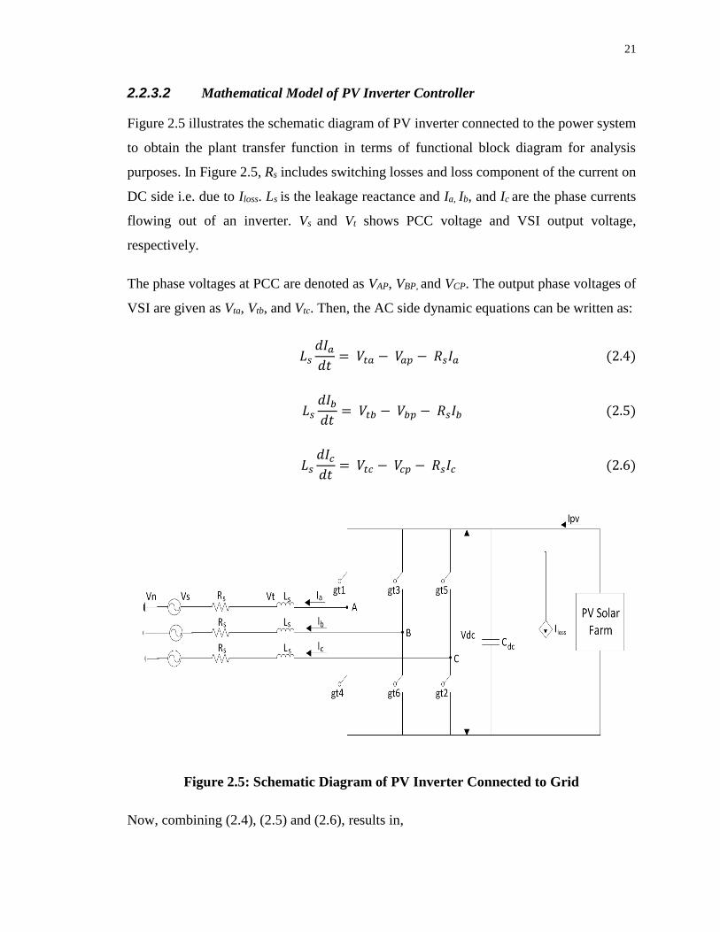
2.2.3.2 Mathematical Model of PV Inverter Controller
Figure 2.5 illustrates the schematic diagram of PV inverter connected to the power system
to obtain the plant transfer function in terms of functional block diagram for analysis
purposes. In Figure 2.5, Rs includes switching losses and loss component of the current on
DC side i.e. due to Iloss. Ls is the leakage reactance and Ia, Ib, and Ic are the phase currents
flowing out of an inverter. Vs and Vt shows PCC voltage and VSI output voltage,
respectively.
The phase voltages at PCC are denoted as VAP, VBP, and VCP. The output phase voltages of
VSI are given as Vta, Vtb, and Vtc. Then, the AC side dynamic equations can be written as:
𝐿𝑠
𝑑𝐼𝑎𝑑𝑡
= 𝑉𝑡𝑎 − 𝑉𝑎𝑝 − 𝑅𝑠𝐼𝑎 (2.4)
𝐿𝑠
𝑑𝐼𝑏𝑑𝑡
= 𝑉𝑡𝑏 − 𝑉𝑏𝑝 − 𝑅𝑠𝐼𝑏 (2.5)
𝐿𝑠
𝑑𝐼𝑐𝑑𝑡
= 𝑉𝑡𝑐 − 𝑉𝑐𝑝 − 𝑅𝑠𝐼𝑐 (2.6)
Figure 2.5: Schematic Diagram of PV Inverter Connected to Grid
Now, combining (2.4), (2.5) and (2.6), results in,

22
𝑝 [𝐼𝑎𝐼𝑏𝐼𝑐
] =
[ −
𝑅𝑠
𝐿𝑠0 0
0 −𝑅𝑠
𝐿𝑠0
0 0 −𝑅𝑠
𝐿𝑠]
[𝐼𝑎𝐼𝑏𝐼𝑐
] + 1
𝐿𝑠[
𝑉𝑡𝑎 − 𝑉𝑎𝑝
𝑉𝑡𝑏 − 𝑉𝑏𝑝
𝑉𝑡𝑐 − 𝑉𝑐𝑝
] (2.7)
where, p is operator for 𝑑
𝑑𝑡. Applying transformation equation (2.3) for abc reference frame
to dq synchronous rotating reference frame on (2.7), the following equation is obtained:
𝐿𝑠
𝑑
𝑑𝑡[𝐼𝑑𝐼𝑞
] = [−𝑅𝑠 𝐿𝑠𝜔−𝐿𝑠𝜔 −𝑅𝑠
] [𝐼𝑑𝐼𝑞
] + [𝑉𝑡𝑑 − 𝑉𝑑
𝑉𝑡𝑞 − 𝑉𝑞] (2.8)
Subscript ‘d’ and ‘q’ represent electrical quantities in direct axis and quadrature axis
reference frame, respectively.
2.2.3.3 Phase Locked Loop (PLL) Oscillator Design
The PCC voltages (VAP, VBP, and VCP) are given to the PLL block available in
PSCAD/EMTDC software to obtain the synchronization angle 𝜃. The offset angle of 1.57
rad (90 degree) has been used to make the alignment of direct axis component (Vd) with
the voltage vector in abc frame. Therefore, in steady state quadrature axis component (Vq)
of AC voltage can be considered as zero.
2.2.3.4 Real and Reactive Power Output Control from VSI
According to (2.3), output power equations of a voltage source inverter are calculated.
Therefore, real power (P) and reactive power (Q) in dq frame is as follows:
𝑃 = 3
2(𝑉𝑑𝐼𝑑 + 𝑉𝑞𝐼𝑞) (2.9)
𝑄 = 3
2(𝑉𝑞𝐼𝑑 − 𝑉𝑑𝐼𝑞) (2.10)

23
As mentioned in Section 2.2.3.3, the alignment of direct axis component (Vd) with the
voltage vector in abc frame makes 𝑉𝑠𝑞 = 0 through PLL. Hence, equations (2.9) and (2.10)
can be rewritten as
𝑃 = 3
2(𝑉𝑑𝐼𝑑) (2.11)
𝑄 = −3
2(𝑉𝑑𝐼𝑞) (2.12)
Now, the power output from VSI will be controlled by 𝐼𝑑 and 𝐼𝑞 as 𝑉𝑑 is the grid voltage
and does not change significantly. To have unity power factor correction, the reference
value of reactive power output of the inverter is set to zero. Hence, according to equation
(2.12), 𝑄 = 0. The desired current output from VSI to get reference power Pref and Qref
become:
𝐼𝑑𝑟𝑒𝑓 = 2
3𝑉𝑑𝑃𝑟𝑒𝑓 (2.13)
𝐼𝑞𝑟𝑒𝑓 = 0 (2.14)
2.2.3.5 Output Voltage Vector of VSI in Synchronous Reference Frame
After employing sinusoidal pulse width modulation (SPWM) technique [32] for generating
firing pulses for switches, the output voltage from VSI in Figure 2.5 is as follows:
𝑉𝑡𝑎 = 𝑚𝑎(𝑡)𝑉𝑑𝑐
2 (2.15)
𝑉𝑡𝑏 = 𝑚𝑏(𝑡)𝑉𝑑𝑐
2 (2.16)
𝑉𝑡𝑐 = 𝑚𝑐(𝑡)𝑉𝑑𝑐
2 (2.17)

24
Here, 𝑚𝑎, 𝑚𝑏,𝑚𝑐 are the modulation indexes of the inverter and 𝑉𝑑𝑐 is the voltage of DC
link capacitor.
Further, fundamental components of the switching pulses are as follows:
𝑚𝑎1= 𝑘 sin(𝜔𝑡 + 𝛼) (2.18)
𝑚𝑏1 = 𝑘 sin(𝜔𝑡 + 𝛼 − 2𝜋
3⁄ ) (2.19)
𝑚𝑐1= 𝑘 sin(𝜔𝑡 + 𝛼 + 2𝜋
3⁄ ) (2.20)
where, 𝑘 is the modulation index, which should be less than 1 for linear operation of
inverter. After neglecting voltage harmonics produced by VSI, the fundamental output
voltage from Figure 2.5 is
𝑉𝑡𝑎1= 𝑚𝑎1
(𝑡)𝑉𝑑𝑐
2 (2.21)
𝑉𝑡𝑏1= 𝑚𝑏1
(𝑡)𝑉𝑑𝑐
2 (2.22)
𝑉𝑡𝑐1= 𝑚𝑐1
(𝑡)𝑉𝑑𝑐
2 (2.23)
Therefore, the net output voltage obtained after applying abc to dq transformation (2.3) is
𝑉𝑡 (𝑡) = (𝑉𝑡𝑑 + 𝑗𝑉𝑡𝑞)𝑒
𝑗𝜔𝑡 (2.24)
where,
𝑉𝑡𝑑 = 𝑉𝑑𝑐
2𝑚𝑑 (2.25)
and

25
𝑉𝑡𝑞 = 𝑉𝑑𝑐
2𝑚𝑞 (2.26)
2.2.3.6 Inner Current Control Loop
Substituting values of 𝑉𝑡𝑑 and 𝑉𝑡𝑞 from (2.25) and (2.26) in (2.8) results in:
𝐿𝑠
𝑑𝐼𝑑𝑑𝑡
= −𝑅𝑠𝐼𝑑 + 𝐿𝑠𝜔𝐼𝑞 +𝑉𝑑𝑐
2𝑚𝑑 − 𝑉𝑑 (2.27)
𝐿𝑠
𝑑𝐼𝑞
𝑑𝑡= −𝑅𝑠𝐼𝑞 − 𝐿𝑠𝜔𝐼𝑑 +
𝑉𝑑𝑐
2𝑚𝑞 − 𝑉𝑞 (2.28)
The control of Id and Iq needs to be decoupled to have decoupled control of output power.
The term 𝐿𝑠𝜔 in above equations represents coupling in a system. Now, by
decoupling 𝐼𝑑 and 𝐼𝑞, the equation for 𝑚𝑑 and 𝑚𝑞 is:
𝑚𝑑 = 2
𝑉𝑑𝑐(𝑈𝑑 − 𝐿𝑠𝜔𝐼𝑞 + 𝑉𝑑) (2.29)
𝑚𝑞 = 2
𝑉𝑑𝑐(𝑈𝑞 + 𝐿𝑠𝜔𝐼𝑑 + 𝑉𝑞) (2.30)
In the above equations, 𝑈𝑑 and 𝑈𝑞 are control inputs, and 𝐿𝑠𝜔𝐼𝑑 and 𝐿𝑠𝜔𝐼𝑞 are decoupling
feed forward inputs. The equation then simplifies to:
𝐿𝑠
𝑑𝐼𝑑𝑑𝑡
= −𝑅𝑠𝐼𝑑 + 𝑈𝑑 (2.31)
𝐿𝑠
𝑑𝐼𝑞
𝑑𝑡= −𝑅𝑠𝐼𝑞 + 𝑈𝑞 (2.32)
Equations (2.31) and (2.32) describe two first order decoupled systems. Figure 2.6 shows
the block diagram of an inner loop control of inverter controller. Here, 𝐼𝑑𝑟𝑒𝑓 is compared
with Id which gives an error signal. This error signal is fed to PI-1 controller whose resultant

26
is 𝑈𝑑. Here, 𝐼𝑑𝑟𝑒𝑓 and 𝐼𝑞𝑟𝑒𝑓 are reference currents for real and reactive power, respectively.
The PI controller parameters 𝐾𝑝 and 𝑇𝑖 for PI-1 are selected by systematic trial and error
method to meet the specific requirements. These specific requirements are to obtain a quick
rise time, minimum settling time and a peak overshoot less than 10% in the reactive power
output of PV solar farm. Equation (2.29) is implemented with 𝑈𝑑 to get 𝑚𝑑. Similar
procedure is carried out by using equation (2.30) for obtaining 𝑚𝑞[79]. The PI control
parameters for PI-2 are also selected by systematic trial and error method meet the specific
objectives which are a quick rise time, minimum settling time and a peak overshoot less
than 10% in the real power output of PV solar farm. Two limiters are used to limit the
modulation indexes 𝑚𝑑 and 𝑚𝑞. The values of PI controllers are mentioned in Appendix-
D.
Figure 2.6: Block Diagram of Inner Loop VSI Current Controller
2.2.3.7 Sinusoidal Pulse Width Modulation (SPWM) Technique [32]:
The output modulation signals of the inner loop control 𝑚𝑑 and 𝑚𝑞 are fed to dq to abc
block to get the three phase modulation signals 𝑚𝑎, 𝑚𝑏 and 𝑚𝑐. This transformation is
done by inverting the matrix given in (2.3). The dq to abc transformation matrix is as
follows:

27
[
𝑚𝑎(𝑡)𝑚𝑏(𝑡)𝑚𝑐(𝑡)
] =
[
cos(𝜃) − sin(𝜃)
cos (𝜃 +2𝜋
3) − sin (𝜃 +
2𝜋
3)
cos (𝜃 −2𝜋
3) − sin (𝜃 −
2𝜋
3)]
[𝑚𝑑
𝑚𝑞] (2.33)
Here, 𝜃 is the synchronization angle obtained from PLL. Figure 2.7 is reproduced from
[80]. It demonstrates the Sinusoidal Pulse Width Modulation (SPWM) technique from VSI.
The modulation signals 𝑚𝑎, 𝑚𝑏 and 𝑚𝑐 are compared with triangular wave, also known
as carrier wave having a switching frequency of 5 kHz. If modulation signal is greater than
triangular wave then it gives +𝑉𝑑𝑐
2 and when modulation signal is smaller than triangular
wave then it gives −𝑉𝑑𝑐
2. Hence, taking an average over carrier wave time period, the output
voltage appears as a sinusoidal output.
Figure 2.7: Sinusoidal Pulse Width Modulation Technique for VSI [82]
2.2.4 DC Link Capacitor
The main role of DC link capacitor in PV solar system is not only to maintain constant DC
voltage but also to govern the power quality on DC side which ultimately affects the power
28
quality on AC side [83]. The size of DC link capacitor must be carefully chosen while
using converter-less MPPT system. A ripple free DC current and voltage is required at the
input of an inverter for its smooth operation. A very high value of capacitor results in
pulsated power while very low value for capacitor results in power ripples. Therefore, the
DC link capacitor needs to be properly modeled and control.
2.2.4.1 DC Link Capacitor Modeling
A large size DC link capacitor is used for handling maximum power ( 𝑃𝑚𝑎𝑥) [83]. The total
energy (𝑃𝑚𝑎𝑥) for a period of one cycle for handling maximum power at frequency 𝑓 is:
𝐸𝑚𝑎𝑥 = 𝑃𝑚𝑎𝑥
𝑓 (2.34)
Equation (2.34) represents the total energy supplied by DC link capacitor in worst case. It
does not allow the voltage to go below the minimum DC voltage margin i.e. 𝑉𝑑𝑐𝑚𝑖𝑛.
Therefore, total energy can be expressed as:
𝐸𝑚𝑎𝑥 = 𝐶(𝑉𝑑𝑐
2 − 𝑉𝑑𝑐𝑚𝑖𝑛2 )
2 (2.35)
The size of DC link capacitor from equation (2.34) and (2.35) is as follows:
𝐶 = 2𝑃𝑚𝑎𝑥
𝑓𝑉𝑑𝑐2 (1 − 𝐾2)
𝐹𝑎𝑟𝑎𝑑 (2.36)
Here, K is known as ripple factor given by:
𝐾 =𝑉𝑑𝑐𝑚𝑖𝑛
𝑉𝑑𝑐 (2.37)
Equation (2.36) is chosen such that by tuning of inverter controller parameters 𝐾𝑝 and 𝑇𝑖,
the controllability of source current can be achieved at all operating points. Here, it is
assumed that the output of current is ripple free in determination of the size of DC link
capacitor.

29
2.2.4.2 DC Link Voltage Control
As shown in Figure 2.2(d), DC link voltage (𝑉𝑑𝑐) is maintained constant at a reference set
by comparing with MPPT reference voltage (𝑉𝑚𝑝𝑝𝑟𝑒𝑓). The output of this is fed to PI-3
controller. The controller parameters 𝐾𝑝and 𝑇𝑖 for PI-3 are selected by systematic trial and
error method to meet the specific requirements. These specific requirements are to obtain
a quick rise time, minimum settling time and a peak overshoot less than 10% in 𝑉𝑑𝑐. The
output of PI-3 is the direct axis current control reference 𝐼𝑑𝑟𝑒𝑓.
2.2.5 LCL Filter Modeling and Design
Figure 2.2(c) depicts the LCL filter. The inverter output generates harmonics along with
the fundamental component depending on the size of DC link capacitor and switching
frequency. Therefore, AC side of inverter output needs to be filtered properly to avoid
unwanted harmonics. The net harmonics in the filtered output are expressed in terms of
Total Harmonic Distortion (THD) and Total Demand Distortion (TDD). These quantities
should comply with grid code requirements as set by IEEE 519 [84], IEEE 1547 [38], etc.
There are different types of filter configurations that can be used for filtering inverter output
such as L filter comprising only series inductor, LC filter having series inductor with shunt
capacitor and LCL filter comprising two series inductors and a shunt capacitor in ‘T’
configuration. Out of these, the LCL filter is widely used due to its advantages [85,86].
LCL filter achieves better attenuation than LC filter along with cost savings and overall
reduction of the number of components [87]. LCL filter can prevent inrush current at grid
interconnection point by providing inductive output compared to LC filter. By using small
values of inductors and capacitors in LCL filter, good performance can be obtained up to
hundreds of kW [88]. Therefore, LCL filter is used in this thesis.
In modeling the LCL filter, certain characteristics must be considered such as filter size,
switching ripple attenuation and current ripple. IGBT switching and conduction losses
depend on current ripple. Therefore, smaller ripple current results in lower switching and
conduction losses. Also, a large size of inductor results in high coil and core losses. Hence,

30
the inductor needs to be designed properly as a trade-off is seen between size of an inductor
and different types of losses. The base impedance and base capacitance are defined as [89]
𝑍𝑏 =𝑉𝐿𝐿
2
𝑃𝑛 (2.38)
𝐶𝑏 =1
𝜔𝑔𝑍𝑏 (2.39)
Here, 𝜔𝑔 = 2𝜋𝑓𝑔 where 𝑓𝑔 is grid frequency 60 Hz
𝑉𝐿𝐿 is line to line output voltage on AC side of an inverter = 230 V
𝑃𝑛 is maximum rated power of an inverter = 7.5 MW
Maximum power factor variation seen by load is considered as 5%. Therefore, while
designing the filter capacitance, maximum base impedance of the system is as follows:
𝐶𝑓 = 0.05𝐶𝑏 (2.40)
Hence from equation (2.40), the value of filter capacitance is found to be 1.88 mF.
Typically, ripple current can be chosen as 10%~ 20% of the rated current [87]. Here, we
have considered it as 10%. The maximum current ripple at the output of VSI is given as
[87]:
∆𝐼𝐿𝑚𝑎𝑥 = 0.1𝐼𝑚𝑎𝑥 (2.41)
where,
𝐼𝑚𝑎𝑥 =𝑃𝑛 √2
3𝑉𝑝ℎ (2.42)
and
∆𝐼𝐿𝑚𝑎𝑥 =𝑉𝐷𝐶
6𝑓𝑠𝑤𝐿1 (2.43)

31
Here, 𝑉𝐷𝐶 is DC link voltage, 𝑉𝑝ℎ is the phase voltage on AC side of an inverter and 𝑓𝑠𝑤 is
switching frequency of 5 kHz. Therefore, from (2.41), (2.42) and (2.43), value of 𝐿1 can
be found out. This results in 𝐿1 to be 6.79 µH. The harmonics generated by the inverter
into the grid is found out as follows [87]:
𝐼2(ℎ)
𝐼𝑖(ℎ)=
1
|1 + 𝑟[1 − 𝐿1 𝐶𝑏𝜔𝑠𝑤2 𝑥]|
= 𝑘𝑎 (2.44)
and
𝐿2 = √
1
𝑘𝑎2 + 1
𝐶𝑓𝜔𝑠𝑤2
(2.45)
Here, 𝑘𝑎 is the desired attenuation and is set to 10%. Hence, the value of 𝐿2 is found to be
0.5 µH. There will be a resonance or ringing effect in the system due to presence of L and
C together. To avoid this, a resistor is connected in series with capacitor known as damping
resistor 𝑅𝑓 [87]:
𝑅𝑓 = 1
3𝜔𝑟𝑒𝑠𝐶𝑓 (2.46)
where,
𝜔𝑟𝑒𝑠 = √𝐿1 + 𝐿2
𝐿1𝐿2𝐶𝑓 (2.47)
At resonant frequency, the capacitor filter impedance should be three times of value of
damping resistor [87]. For this, the value of resonant frequency must be within the range
of 10𝑓𝑔and 0.5𝑓𝑠𝑤.
2.2.6 Step Up Transformer
Figure 2.2 illustrates the step up transformer. The output voltage of a VSI is 230 V while
it is connected to the 27.6 kV grid at PCC. Therefore, a coupling transformer known as
step up transformer is connected between the inverter and grid. As per utility connection
requirements [90], the inverter side coupling transformer should be delta and grid side
should be wye grounded. The advantages of such connections are described in [91]. DC

32
terminal is grounded to have equal DC voltage across each IGBT valves. Zero sequence
current flowing through IGBT valves are prevented during SLG fault on AC side of an
inverter by using delta connection on AC side of an inverter. Therefore, in this thesis ∆-Y
(inverter-grid) step up transformer is considered. The transformer parameters are specified
in Appendix-C.
2.3 SHORT CIRCUIT CURRENT CONTROLLER DESIGN
2.3.1 Concept
Short circuits are typically characterized by a substantially high magnitude and distortion
of the current waveform. Hence these can be critical features for detecting a short circuit
condition. Rise in magnitude of current from its maximum allowable limit confirms that
there is some kind of an undesirable event taking place in the system (except transformer
energization, capacitor switching or overload). A novel solar inverter short circuit current
management technique has been patented [10,11] according to which the SCC controller
detects a short circuit or fault condition and shuts off the PV inverter within 1-2
milliseconds. This technique is based on the slope and magnitude of the inverter current
just after the inception of the fault. When a fault occurs, if the slope of the current waveform
exceeds the maximum limit under normal operation (under no fault) the fault is detected
and the inverter is shut off. Further, if the inverter current magnitude exceeds the rated
inverter current, the fault is detected and the inverter is shut off in less than 1 cycle.
2.3.2 Short Circuit Current Controller Module
The block diagram of short circuit current controller as proposed in [8,9] is shown in Figure
2.8. The short circuit current controller consists of three identical channels to measure the
instantaneous output currents of an inverter; IA, IB and IC for phase A, B and C, respectively.
These currents are passed through a low pass filter to reject all higher order frequencies
due to PV inverter injection, transformer energization and capacitor switching, etc [92]. A
time delay of typically 1 second is added through a comparator to avoid a false operation
of the controller due to start up transient of a solar farm. The output of the comparator
becomes HIGH when time is greater than 1 second.
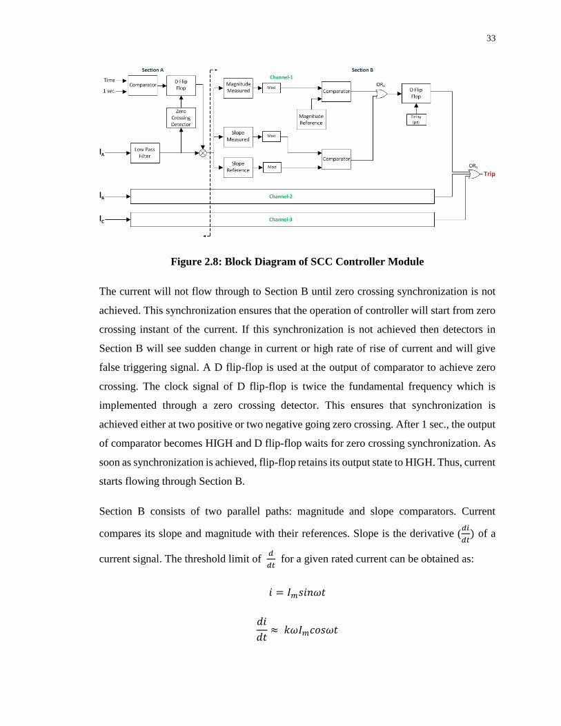
33
Figure 2.8: Block Diagram of SCC Controller Module
The current will not flow through to Section B until zero crossing synchronization is not
achieved. This synchronization ensures that the operation of controller will start from zero
crossing instant of the current. If this synchronization is not achieved then detectors in
Section B will see sudden change in current or high rate of rise of current and will give
false triggering signal. A D flip-flop is used at the output of comparator to achieve zero
crossing. The clock signal of D flip-flop is twice the fundamental frequency which is
implemented through a zero crossing detector. This ensures that synchronization is
achieved either at two positive or two negative going zero crossing. After 1 sec., the output
of comparator becomes HIGH and D flip-flop waits for zero crossing synchronization. As
soon as synchronization is achieved, flip-flop retains its output state to HIGH. Thus, current
starts flowing through Section B.
Section B consists of two parallel paths: magnitude and slope comparators. Current
compares its slope and magnitude with their references. Slope is the derivative (𝑑𝑖
𝑑𝑡) of a
current signal. The threshold limit of 𝑑
𝑑𝑡 for a given rated current can be obtained as:
𝑖 = 𝐼𝑚𝑠𝑖𝑛𝜔𝑡
𝑑𝑖
𝑑𝑡≈ 𝑘𝜔𝐼𝑚𝑐𝑜𝑠𝜔𝑡
34
|𝑑𝑖
𝑑𝑡|𝑚𝑎𝑥
≈ 𝑘𝜔𝐼𝑚 (2.48)
In the equation (2.48), 𝑐𝑜𝑠𝜔𝑡 = 1 for maximum 𝑑𝑖
𝑑𝑡
𝑘 is the tolerance constant
𝜔 = 2𝜋𝑓 is the angular frequency
𝐼𝑚 is the maximum rated current
The value of magnitude reference is considered by choosing an arbitrarily tolerance
constant. The value of 𝑘 can be chosen depending on the value of utility requirements. This
can be any value above 100% or 1 p.u. of rated current. Two absolute value or modulus
detectors has been used prior to slope comparator and one modulus block before magnitude
comparator to avoid its comparison with negative signals.
If any one of the six possible signals from all the three channels violates or exceeds their
threshold limits then signal from the comparator is passed to their respective ORa gate. Its
output is followed by D flip-flop and finally the signal is passed through ORb gate to
generate ‘Trip’ signal. However, before passing it through ORb gate, an intentional delay
of few microseconds (µs) is added. It has been noted that current signals from transient
events such as transformer energization, load switching and capacitor energization which
are not completely filtered out by low pass filter can cause high 𝑑𝑖
𝑑𝑡 for a short period of
time. Therefore, to avoid the generation of an undesired tripping signal, an intentional delay
of few µs is added to clock of D flip-flop. After considering this, the output from D flip-
flop is generated. Once the process of fault detection gets completed, triggering signals
from all the three phases (whichever exceeds their reference limits) are sent to the input of
ORb gate. The output of ORb gate will result in ‘Trip’ signal. The salient feature of the short
circuit current controller is that only one trip signal is needed to disconnect the inverter
based DGs from the grid.
35
The firing pulses along with ‘Trip’ signal are applied to the gating signals of an inverter
through AND gate as shown in Figure 2.2. As soon as the 'Trip' signal becomes high upon
detection of fault, gating signals to all IGBTs of an inverter generated through inverter
controller are immediately turned off through ANDing operation. As a result, within a few
hundred microseconds no power is transferred from the PV solar inverter to the grid.
Once the gating signals of an inverter are turned off, it is expected that the DC voltage
across capacitor will start increasing due to incoming current from PV module. According
to the PV module I-V characteristics, the output current from PV panel gradually decreases
with the increase in voltage and eventually stops at the open rated circuit voltage of the PV
module. Therefore, to reduce the voltage stress across each IGBT switch, and also across
the DC link capacitor, the same triggering signal 'Trip' is utilized to disconnect the PV
modules from the PV inverter. This is achieved by applying the Trip signal to disconnect
the gate turn-off (GTO) thyristors based solid state breaker shown in Figure 2.2(f).
It is necessary to isolate the AC filter capacitor to prevent high ringing currents between
filter capacitance and inductance of the distribution network. Hence, back-to-back GTOs
are connected as shown in Figure 2.2(c) to disconnect AC filter capacitor. As a result, upon
detection of fault, the 'Trip' signal is applied to these GTO switches for isolating AC filter
capacitor from inductor.
After the fault is cleared, a reset signal (not shown) is given to the controller to reset all
triggering signals as well as the flip-flops to bring the PV system back to normal operation.
The entire operation of fault current controller is depicted in the flowchart as shown in
Figure 2.9.

36
No
PV Inverter Starts.
Fault Current Controller is Disabled
Inverter output current IA, IB, IC passes
through filter
PV system generates power with synchronized fault
detector
Monitoring of PV inverter output current
through di/dt and peak magnitude comparators
Zero crossing synchronization of current through D flip
flop and fault current controller is enabled
di/dt > Preset value
or |I|> Irated
'Trip Signal' remains
Low
After certain amount of time delay in clock signal of D
flip - flop, 'Trip' Signal becomes High
'Trip' signal disconnects gating signals, PV
modules from inverter and AC filter capacitor
PV inverter disconnected
from grid
No
Yes
Time Delay 1 sec.
Figure 2.9: Flow Chart of SCC Controller

37
2.3.3 Performance of Short Circuit Current Controller Module
Actual short circuit current waveforms for commercial inverters are obtained from
Southern California Edison Testing lab. These waveforms are utilized to confirm the
successful operation of the short circuit controller. The concept of this short circuit
controller is illustrated below.
Figure 2.10(a) and 2.10(b) demonstrate the SCE lab results of inverter output current during
single line to ground fault for phase A and phase B, respectively. In Figure 2.10(a) and
2.10(b), the green waveform shows the recreated healthy current (no fault condition), red
waveform shows the original fault current and blue waveform shows the fault current
which is filtered (as per the procedure described later). An arrow is drawn in Figure 2.10(a)
and (b), which shows the point of fault inception. It is noticed from Figure 2.10(a) that the
magnitude of the inverter output current increases from 32.0A to 42.8A which is 1.34 p.u.
Furthermore, it is easily observed from the Figures below that the slope of the original
faulted current waveform changes after the instant of fault inception. Under no fault
condition, the current should actually follow the path of recreated healthy waveform. It is
noted that after fault occurs, the original current waveform becomes very noisy and
distorted. Therefore the original fault current waveform is filtered to remove high
frequency noise components and unwanted spikes. It is seen from the Figure 2.10(a) and
(b) that filtered faulted signal (blue waveform) also changes its slope after the occurrence
of the fault. This change in slope is utilized by the short circuit controller to detect the fault
and shut off the inverter.
Similarly, Figures 2.11 and 2.12 depict the SCE lab results of inverter output current for
LL and LLG fault. In both the fault cases, rise in magntiude and change in slope of current
waveform can be noticed from the point of fault inception. Thus, if the slope and magnitude
of inverter current are monitored continuously, the fault can be detected and accordingly
the inverter can be shut off without injecting any short circuit current into the grid.

38
2.3.3.1 Single-Line Ground Fault
Green - Recreated Healthy Waveform
Red - Original Faulted Waveform
Blue - Filtered Faulted Waveform
(a)
(b)
Figure 2.10: Inverter Output Current for SLG Fault (a) Phase A (b) Phase B
Fault Inception
Fault Inception

39
2.3.3.2 Line - Line Fault
Green - Recreated Healthy Waveform
Red - Original Faulted Waveform
Blue - Filtered Faulted Waveform
(a)
(b)
Figure 2.11: Inverter Output Current for LL Fault (a) Phase A (b) Phase B
Fault
Inception
Fault
Inception

40
2.3.3.3 Line - Line - Ground Fault
Green - Recreated Healthy Waveform
Red - Original Faulted Waveform
Blue - Filtered Faulted Waveform
(a)
(b)
Figure 2.12: Inverter Output Current for LLG Fault (a) Phase A (b) Phase B
Fault
Inception
Fault
Inception

41
2.4 CONCLUSION
This chapter presents the modeling and design of a 7.5 MW PV solar system incorporated
with a novel patented short circuit current controller. The study system model is a typical
feeder used in Ontario-Canada for which the short circuit current contribution has already
reached to its maximum limit. The inverter control modeling, selection of filter parameters
and DC link capacitor are explained.
The concept and operation of short circuit current controller for PV inverter based DGs
have been described. The SCC controller technique is based on monitoring of the
slope (𝑑𝑖
𝑑𝑡) of current along with the magnitude |I|. As soon as the tripping signal is
generated on the detection of fault that may lead to a short circuit current contribution from
the inverter beyond the rated inverter current, it (a) disables firing pulses of an inverter (b)
disconnects PV solar farm from the inverter and (c) isolate the filter capacitor from PCC.
The SCC controller will shut off the PV inverter within 1-2 milliseconds from the initiation
of any fault in the grid without exceeding maximum rated value of inverter current at PCC.
Therefore, the power system network does not see any short circuit current contribution
from PV inverter.

42
CHAPTER 3
ELECTROMAGNETIC TRANSIENTS SIMULATION USING PSCAD SOFTWARE
3.1 INTRODUCTION
This chapter presents the implementation of short circuit current (SCC) controller based on
the rate of rise of current detection and the current magnitude detection in a PV solar system
based DG. The performance of SCC controller is analyzed in electromagnetic transient
simulation software - PSCAD/EMTDC. Case studies are performed by applying different
types of faults at PCC with fault current controller enabled. To understand the effectiveness
of SCC controller, faults are applied at different time instants and their results are
investigated. Moreover, a large load switching is simulated to ensure that the controller
does not respond to such an event since it is expected to respond only to faults.
Section 3.2 describes the system model; Section 3.3 details the implementation of short
circuit current controller in PSCAD software; Sections 3.4 and 3.5 depict the simulation
results for asymmetrical and symmetrical faults, respectively, with the SCC controller
incorporated. In Section 3.6, a study of faults at different time instants is presented; Section
3.7 shows the response of proposed controller during load switching events. Finally,
Section 3.8 concludes the outcome of this work.
3.2 SYSTEM MODEL
A typical 27.6 kV feeder in Ontario, Canada, that is 25 km long as described in Section
2.2, is considered here as the study system. A 7.5 MW PV solar system is connected at the
end of a feeder. Figure 3.1 presents the detailed PV inverter system with incorporated short
circuit current controller module. The system consists of the solar farm as shown in Figure
3.1 (a), voltage source inverter in Figure 3.1 (b), LCL filter as described in Figure 3.1 (c),
inverter controller as depicted in Figure 3.1 (d).

43
Figure 3.1: System Model with PV System Inverter, Conventional Controller and
the incorporated Short Circuit Current Controller in PSCAD/EMTDC

44
The modeling of PV source, inverter control and LCL filter are described in Sections 2.2.2,
2.2.3 and 2.2.5, respectively. The PV inverter output of 230 V connects to the grid through
a 0.23/27.6 kV, 7.5 MVA step up transformer. The parameters of LCL filter are described
in Section 2.6. A novel controller for restricting short circuit current from PV inverter is
incorporated with the conventional PV inverter controller as shown in Figure 3.1 (e). Figure
3.1 (f) represents the GTO based switch used to isolate the solar panels during short circuit
scenarios. The output of short circuit current controller module is given to the firing pulses
of an inverter and AC filter. As soon as the fault condition is established that can cause the
inverter current to exceed its rated magnitude, firing pulses are disabled and the filter gets
disconnected from the network
3.3 IMPLEMENTATION OF SCC CONTROLLER IN PSCAD SOFTWARE
Figure 3.2 shows the implementation of short circuit current controller as proposed in
[10,11] in PSCAD software. The Figure consists of two sections: Section A and Section B.
Also, it has three identical channels: Channel - 1, 2 and 3 are for inverter output phase
currents IA, IB and IC, respectively. The detailed implementation of Channel - 1
corresponding to phase A current is described below.
Figure 3.2: Implementation of SCC Controller in PSCAD

45
The inverter output current IA passes through transfer function filter (𝐻 = 𝐺
1 +𝑠𝜏), which
acts as a low pass filter. The parameters of LPF filter are Gain (G) = 1 and Time Constant
(𝜏) = 0.0001 second. The filter parameters are very much sensitive to the fault. The value
of time constant should be selected appropriately such that it should not respond to any
switching spike. The use of G = 1 does not suppress or increase the magnitude of inverter
output current. Hence, the actual inverter current magnitude can be seen from the output of
low pass filter. The value of time constant is determined through cut-off frequency (𝑓𝑐) of
1kHz (𝜏 = 1
2𝜋𝑓𝑐). The cut-off frequency is selected in such a way that filter introduces less
delay and gives good filtering performance. The delay introduced by the filter can either
be calculated through group or phase delay. The group delay is defined as the derivative of
the phase with respect to angular frequency and is a measure of the distortion in the signal
introduced by phase differences for different frequencies. Phase delay is a measure of the
time delay of the phase experienced by each sinusoidal component of the input signal.
Therefore, the delay introduced by the filter at 60 Hz frequency is calculated as follows:
𝑃ℎ𝑎𝑠𝑒 𝐷𝑒𝑙𝑎𝑦 = tan−1(𝜔𝑅𝐶)
As 𝜏 = RC,
𝑃ℎ𝑎𝑠𝑒 𝐷𝑒𝑙𝑎𝑦 = tan−1(𝜔𝜏)
𝑃ℎ𝑎𝑠𝑒 𝐷𝑒𝑙𝑎𝑦 = 2.16° (3.1)
where, 𝜔 is the angular grid frequency 2πf = 377 rad/sec
𝜏 is the time constant = 0.0001 sec
The time period of a 60 Hz signal for one cycle (360°) is 16.67 ms. The presence of low
pass filter gives an extra phase delay of 2.16° which is equivalent to a delay of 0.1 ms at
60 Hz frequency.
An intentional delay of 1 second is added to comparator to avoid any false operation due
to the start-up transient of solar farm. No current passes through Section B until zero

46
crossing synchronization is achieved in Section A. A zero crossing detector is introduced
in the clock signal of D flip-flop. This circuitry guarantees that this controller starts
operating at the zero crossing of current after one second. If this zero cross detector is not
used there will be a mismatch at the beginning between 𝑑𝑖
𝑑𝑡 and the input. As soon as the
zero crossing synchronization is achieved, current starts flowing through Section B.
Subsequently, current flows in two parallel paths: magnitude and slope comparator. The
magnitude and slope of the inverter current are compared with their reference values or
maximum permissible limits.
The peak magnitude of the inverter current for 7.5 MW PV solar system connected to the
LT side of the coupling transformer having voltage level of 230 V is calculated as follows:
𝐼𝑚 = √2
√3
𝑃𝑚
𝑉𝐿𝐿= 26.6 𝑘𝐴
where, 𝑃𝑚 is the maximum rated power = 7.5 MW
𝑉𝐿𝐿 is the line to line inverter output voltage = 230 V
𝐼𝑚 is the maximum rated current
𝑃𝑚 𝑉𝐿𝐿The maximum allowable limit of the slope of an inverter current is evaluated as
follows:
|𝑑𝑖
𝑑𝑡|𝑚𝑎𝑥
= 𝑘𝜔𝐼𝑚
|𝑑𝑖
𝑑𝑡|𝑚𝑎𝑥
= 10640 𝑎𝑚𝑝𝑠 𝑝𝑒𝑟 𝑠𝑒𝑐.
where, 𝑘 is tolerance constant = 1.06
𝜔 is angular frequency = 377 rad/sec
𝐼𝑚 is the maximum rated current = 26.6 kA

47
As shown in Figure 3.2, a rate limiter has been used for slope comparison. The rate limiter
outputs a duplicate of the input function as long as the rate of change of the input (𝑑𝑖
𝑑𝑡) does
not exceed the specified limits. If the rate of change does exceed the limits, the output falls
ahead or behind the input, confining its rate of change within specified limits. An absolute
value or modulus detector has been used prior to comparators to avoid its comparison with
negative signals. If current exceeds any of its allowable limits (slope or magnitude) then
output of comparator becomes 1 or logical high. The output of magnitude and slope
comparators is followed by D flip-flops D1 and D2, respectively. Now, the signal flows
through D flip-flop with an intentional delay of 10 µs introduced into the clock of flip-flop.
The reason of providing this delay is explained in Section 2.3.2. The outputs of D1 and D2
flip-flops are 'Ma' and 'Triga', respectively. These outputs become high (i.e. 1) on the
detection of fault. Ma, Mb and Mc are the triggering signals of magnitude detectors for
phase A, B and C, respectively. 'MagTrigger' is the output of the ORa gate having input
Ma, Mb and Mc. Thus, output from flip-flops of all the three phase channels are given to
the input of ORb gate to generate the final output triggering signal 'Trip'. This signal will
become high if any of the phase current of inverter output at PCC exceeds its permissible
limits.
Finally, on the fault detection, 'Trip' signal disables firing pulses of an inverter, disconnects
PV solar farm from the inverter and isolates the filter capacitor from PCC as shown in
Figure 3.1, 3.1 (f) and 3.1 (c), respectively.
Studies are performed by applying different types of faults on 7.5 MW PV solar system
connected to the grid with short circuit current controller enabled. Both symmetrical and
asymmetrical faults are applied on PCC at t = 2 second for a duration of 0.1 second or 6
cycles. Studies are also performed by applying different types of faults at different time
instants to study the effectiveness of the SCC controller. Load switching is simulated to
ensure that controller does not respond to such an event and can successfully discriminate
between a fault and an overload condition. The simulation results for each case are
described from Section 3.4 to 3.7.

48
3.4 ASYMMETRICAL FAULT STUDIES
3.4.1 Single Line - Ground Fault
Figure 3.3 shows (a) inverter output current at PCC for single line to ground fault at t = 2
second, (b) generation of triggering signals from SCC controller upon detection of fault
and (c) inverter fault current at PCC with controller enabled.
(a)
(b)

49
(c)
Figure 3.3: (a) Inverter Fault Current at t = 2 sec. (b) Triggering Signals (c)
Inverter Fault Current with SCC Controller
Figure 3.4 depicts the zoomed waveforms of (a) inverter output current for single line to
ground fault at t = 2 second, (b) triggering signals of fault current limiter and (c) inverter
fault current at PCC with short circuit current controller enabled. The waveforms are then
zoomed to understand more clearly the behavior of fault current at PCC and operation of
enabled fault current controller during single line to ground fault.
(a)

50
(b)
(c)
Figure 3.4: Zoomed Waveforms of (a) Inverter Fault Current at t = 2 sec. (b)
Triggering Signals (c) Inverter Fault Current with SCC Controller
Figure 3.3(a) demonstrates that the magnitude of inverter output current at PCC increases
from 1 p.u. to 1.3 p.u. during single line to ground fault. It can be seen from Figure 3.4(a)
that no large transients are observed from initiation of fault at t = 2 second. In Figures
3.3(b) and 3.4(b), Triga, Trigb and Trigc are the triggering signals or output of slope

51
comparator for phase A, B and C, respectively. 'MagTrigger' is the resultant output of
magnitude detector of all the three phases. If magnitude of any of the three phases exceeds
the rated value then 'MagTrigger' gets high. The delay introduced by the filter at 60 Hz
frequency is 0.1ms. The controller will be able to recognize the fault after 0.1ms of its
occurrence. It is noticed from Figure 3.4(b) that 'Trigb' signal has become high after 1.1
ms from the initiation of fault in the grid, as slope of phase B current (𝑑𝑖
𝑑𝑡) has exceeded its
maximum allowable limit. Later, MagTrigger and other triggering signals get high.
However, the noticeable feature of the SCC controller is that only one triggering signal is
needed to disconnect the PV inverter from the grid. As soon as the 'Trigb' signal becomes
high, inverter fault current at PCC starts decreasing as shown in Figure 3.4(c). Finally, it
can be concluded from Figure 3.4 (c) that the PV inverter current at PCC becomes zero
within 1.8 ms upon the response of slope detector. This means that no short circuit current
(in excess of the rated value) flows from the PV inverter to the grid. Therefore, power
system network does not see any short circuit current contribution from PV inverter.
3.4.2 Line - Line Fault
Figure 3.5 shows cases (a) inverter output current at PCC for line to line or line to line to
ground fault at t = 2 second, (b) generation of triggering signals (Triga, Trigb, Trigc and
MagTrigger) from SCC controller upon detection of fault and (c) inverter fault current at
PCC with controller enabled.
To understand the behavior of fault current at PCC and operation of enabled fault current
controller during LL fault, Figure 3.6 illustrates the zoomed waveforms of (a) inverter
output current for LL fault at t = 2 second with SCC controller disabled, (b) triggering
signals of fault current limiter and (c) inverter fault current at PCC with controller enabled.

52
(a)
(b)

53
(c)
Figure 3.5: (a) Inverter Fault Current at t = 2 sec. (b) Triggering Signals (c)
Inverter Fault Current with SCC Controller
(a)

54
(b)
(c)
Figure 3.6: Zoomed Waveforms of (a) Inverter Fault Current at t = 2 sec. (b)
Triggering Signals (c) Inverter Fault Current with SCC Controller
Figure 3.5(a) shows that magnitude of inverter output current at PCC reaches upto 1.4 p.u.
The large transients or distortion of the faulted current waveform can be seen in Figure
3.6(a) after the inception of fault at t = 2 second. The delay introduced by the filter at 60

55
Hz frequency is 0.1ms. It is observed in Figure 3.6(b) that with the SCC controller enabled,
'Trigb' signal has become high within 0.2 ms from the initiation of fault at t = 2 second.
Phase B has violated the maximum permissible limit of rate limiter (𝑑𝑖
𝑑𝑡), so 'Trigb' signal
rises from 0 to 1. 'Trigb' signal is given to gating signals of a PV inverter, solar farm and
AC filter capacitor. PV solar farm modules stop transferring current to the grid within 0.7
ms from the initiation of fault in the grid as shown in Figure 3.6(c). It is also noticed from
Figure 3.6(c), that the current has not exceeded its maximum rated value i.e. 1 p.u.
3.4.3 Line - Line - Ground Fault
The behavior of inverter output current during LLG fault at t = 2 second is found to be
similar to LL fault case (Section 3.4.2). Hence, the simulation results are not presented for
the LLG case.
3.5 SYMMETRICAL FAULT STUDIES
3.5.1 Line - Line - Line Fault
Figure 3.7 depicts (a) Inverter fault current at PCC for LLL fault at t = 2 second with SCC
controller disabled, (b) triggering signals (Triga, Trigb, Trigc and MagTrigger) from SCC
controller upon detection of fault and (c) inverter fault current at PCC with SCC controller
enabled.
Figure 3.8 represents the zoomed waveforms of (a) inverter output current at PCC for LLL
fault at t = 2 second with SCC controller disabled, (b) triggering signals of fault current
limiter upon detection of fault and (c) inverter fault current at PCC with SCC controller
enabled. These waveforms are zoomed to understand more precisely the behavior of fault
current at PCC and operation of fault current controller during symmetrical fault.

56
(a)
(b)

57
(c)
Figure 3.7: (a) Inverter Fault Current at t = 2 sec. (b) Triggering Signals (c)
Inverter Fault Current with SCC Controller
(a)

58
(b)
(c)
Figure 3.8: Zoomed Waveforms of (a) Inverter Fault Current at t = 2 sec. (b)
Triggering Signals (c) Inverter Fault Current with SCC Controller
Figure 3.8(a) demonstrates that the magnitude of inverter output current at PCC during
symmetrical fault increases upto 1.45 p.u. In Figures 3.7(b) and 3.8(b), Triga, Trigb and
59
Trigc are the triggering signals or output of slope comparator for phase A, B and C,
respectively. 'MagTrigger' is the equivalent output of magnitude detector of all the three
phases. The delay introduced by the filter at 60 Hz frequency is 0.1 ms. It is noticed from
Figure 3.8(b) that 'Trigc' signal becomes high within 0.3ms from the initiation of fault in
the grid, as slope of phase C (𝑑𝑖
𝑑𝑡) has violated its permissible limit. Finally from Figure
3.8(c), it is concluded that magnitude of inverter output current at PCC goes to zero in 0.8
ms. This means that no current flows from PV inverter to the grid. In addition, inverter
current does not exceed its maximum rated value. Therefore, power system network does
not see any short circuit current contribution from PV inverter.
From all the above cases (Section 3.4 and 3.5.1), it is observed that response of slope
detector is faster than the magnitude detector. Hence, if the primary slope detector
technique fails to respond the magnitude detector will acts as a secondary detection
technique and would never allow the fault current to exceed its maximum rated value.
3.5.2 Line - Line - Line Ground Fault
Inverter output current during LLLG fault at t = 2 second for 7.5 MW PV solar system
connected to the 27.6 kV grid bus exhibits very similar type of fault current behavior when
LLL fault occurs at PCC. Hence, the simulation results shown in Section 3.5.1 also hold
true for LLLG fault case.
3.6 FAULT STUDIES AT DIFFERENT TIME INSTANTS
In Section 3.4 and 3.5, different types of faults are applied at t = 2 second and response of
short circuit current controller is studied for same time instant of occurrence. To ensure the
effectiveness of SCC controller, both symmetrical and asymmetrical faults are applied at
different time instants and their results are analyzed. The simulation results are described
below.
3.6.1 Asymmetrical Fault
Figure 3.9 shows (a) Inverter fault current at PCC for LLG fault at t = 4.5 second with SCC
controller disabled, (b) generation of triggering signals of fault current limiter upon

60
detection of fault and (c) inverter fault current at PCC with SCC controller enabled. The
fault occurs at t = 4.5 second close to the peak instant of PV inverter current.
(a)
(b)

61
(c)
Figure 3.9: (a) Inverter Fault Current at t = 4.5 sec. (b) Triggering Signals (c)
Inverter Fault Current with SCC Controller
(a)

62
(b)
(c)
Figure 3.10: Zoomed Waveforms of (a) Inverter Fault Current at t = 4.5 sec. (b)
Triggering Signals (c) Inverter Fault Current with SCC Controller
To clearly understand the behavior of fault current at PCC and operation of enabled fault
current controller during LLG fault, Figure 3.10 illustrates the zoomed waveforms of (a)
inverter output current for LLG fault at t = 4.5 second (close to current peak) with SCC

63
controller disabled, (b) triggering signals of fault current limiter and (c) inverter fault
current at PCC with SCC controller enabled.
Figure 3.9(a) demonstrates that the magnitude of inverter output current at PCC increases
from 1 p.u. to 1.45 p.u. during single line to ground fault. It is seen from Figure 3.10(a)
that in this case the fault occurs near the peak instant of an inverter current. In Figures
3.9(b) and 3.10(b), Triga, Trigb and Trigc are the output of slope comparator for phase A,
B and C, respectively. 'MagTrigger' is the equivalent output of magnitude detector of all
the three phases. The delay introduced by the filter at 60 Hz frequency is 0.1 ms. It is
noticed from Figure 3.10(a) that inverter current goes above 1 p.u. after the fault occurs.
As soon as the magnitude of phase B current (|𝐼|𝑚𝑎𝑥) exceeds its allowable limit,
'MagTrigger' signal gets high within 0.7 ms from the initiation of fault in the grid. Inverter
fault current at PCC starts decreasing immediately upon detection of fault as shown in
Figure 3.10(c). Finally, it is concluded from Figure 3.10(c) that inverter current at PCC
reaches zero within 1.3 ms based on the response of magnitude detector. Hence, if the fault
occurs near the peak instant, the response of magnitude detector may be faster than the
slope detector and the inverter current is not allowed to exceed its maximum rated value.
Therefore, there is no apprehension of short circuit current contribution from PV inverter.
3.6.2 Symmetrical Fault
Figure 3.11 demonstrates (a) inverter output current at PCC for LLLG fault at t = 5 second,
(b) generation of triggering signals from SCC controller upon detection of fault and (c)
inverter fault current at PCC with SCC controller enabled. The symmetrical fault occurs at
the positive going zero crossing of phase A, close to the current peak of phase B, and
between the negative going zero crossing and current peak of phase C.
Figure 3.12 depicts the zoomed waveforms of (a) inverter output current at PCC for LLLG
fault at t = 5 second, (b) triggering signals of fault current limiter and (c) inverter fault
current at PCC with SCC controller enabled. The waveforms are zoomed to understand
more clearly the behavior of fault current at PCC and operation of enabled fault current
controller during LLLG fault.

64
(a)
(b)

65
(c)
Figure 3.11: (a) Inverter Fault Current at t = 5 sec. (b) Triggering Signals
(c) Inverter Fault Current with SCC Controller
(a)

66
(b)
(c)
Figure 3.12: Zoomed Waveforms of (a) Inverter Fault Current at t = 5 sec. (b)
Triggering Signals (c) Inverter Fault Current with SCC Controller
Figure 3.11(a) shows that magnitude of inverter output current at PCC reaches up to 1.3
p.u. The large transients or distortion of the faulted current waveform can be seen in Figure
3.12(a) after the inception of fault at t = 5 second. The delay introduced by the filter at 60

67
Hz frequency is 0.1 ms. It is observed from Figure 3.12(b) that with the SCC controller
enabled, 'Trigc' signal becomes high within 0.2 ms from the initiation of fault at t = 5
second. Phase C has violated the maximum permissible limit of rate limiter (𝑑𝑖
𝑑𝑡), so 'Trigc'
signal rises from 0 to 1. Slope detector responds quickly before the current exceeds its peak
rated value. PV inverter is disconnected from the grid within 1 ms from the initiation of
fault in the grid as shown in Figure 3.11(c). It is also noticed from Figure 3.12(c), that the
current has not exceeded its maximum rated value i.e 1 p.u.
3.7 RESPONSE TIME OF SCC CONTROLLER FOR FAULTS AT DIFFERENT TIME INSTANTS
Table 3.1 shows the response time of short circuit current controller for a line-to-line (LL)
fault at different time instants.
LL Fault at Different Time Instant Response Time
Zero Crossing 2 ms
Between Zero Crossing and Positive Peak 0.8 ms
Between Zero Crossing and Negative Peak 0.3 ms
Table 3.1: Response Time of SCC Controller during LL Fault
Table 3.2 shows the response time of short circuit current controller for a line-to-line-to-
line (LLL) fault at different time instants.
LLL Fault at Different Time Instant Response Time
Zero Crossing 2 ms
Between Zero Crossing and Positive Peak 0.3 ms
Between Zero Crossing and Negative Peak 0.9 ms
Table 3.2: Response Time of SCC Controller during LLL Fault

68
3.8 LOAD SWITCHING
Figure 3.13(a) illustrates the PV inverter output current for a load switching event at time
instant t = 1.8 second. Figure 3.13(b) demonstrates the triggering signals for the short
circuit current controller enabled. It is observed that the enabled controller does not respond
to a load switching event of a large feeder load of 60 MW, 0.9 pf. The steep rate of change
in current during the load switching is considered as the slope of high frequency spike
which does not last long. These spikes will be removed by low pass filter (Fig. 3.2).
Even after the filtering, if spikes are not cleared then the time delay introduced in the clock
of D flip-flop will not allow the triggering signal output from ORa gate (Fig. 3.2) to pass
through during this transient event. Hence, a false triggering is avoided at this load
switching event, as discussed earlier in Section 2.3.2 and 3.3. This demonstrates that the
SCC controller can successfully discriminate between a fault and an overload event.
(a)

69
(b)
Figure 3.13: (a) PV Inverter Current with 60 MW, 0.9 pf Load Switching (b)
Triggering Signals from SCC Controller
3.9 CONCLUSION
In this chapter, the performance of the short circuit current controller is validated in
electromagnetic transient simulation software PSCAD on a 7.5 MW PV solar system
connected in a typical distribution feeder of Ontario. The SCC controller technique is based
on monitoring of the slope (𝑑𝑖
𝑑𝑡) of current along with the magnitude |I|. Following
conclusions are drawn:
Different types of asymmetrical faults – SLG, LL, and LLG fault, are applied on
the point of common coupling (PCC) with the SCC controller enabled. PV solar
farm modules stop transferring current to the grid within maximum of 1.8 ms from
the initiation of fault in the grid without exceeding maximum rated value. In these
case studies, slope detector (𝑑𝑖
𝑑𝑡) responds faster than the magnitude detector on the
detection of fault.

70
Studies are also performed for symmetrical faults which occurs rarely in a
transmission line but can potentially cause a severe damage on occurrence. It is
found that PV inverter is disconnected form the grid within maximum 0.8 ms from
the initiation of fault in the grid without exceeding the maximum permissible limit.
Triggering signal is generated on the response of slope detector (𝑑𝑖
𝑑𝑡).
Time instant of fault occurrence is changed to understand the performance of SCC
controller more effectively. An asymmetrical fault (LLG) occurs on grid close to
current peak, the magnitude of inverter output current tends to go beyond its
maximum allowable limit instantly. In this case, the magnitude detector (|𝐼|𝑚𝑎𝑥)
responds faster than the slope detector on the detection of fault. PV solar farm
modules stop transferring current to the grid within 0.7 ms. Furthermore, a
symmetrical fault occurs at the negative going zero crossing. Here, the SCC
controller restricts the PV inverter current completely in 1 ms on the response of
slope detector (𝑑𝑖
𝑑𝑡) without exceeding maximum rated value.
The SCC controller is shown to effectively distinguish between large load
switching event and a fault condition. Hence, the generation of undesired tripping
signal is avoided.
The new SCC controller can successfully disconnect the PV solar farm within 1-2
milliseconds regardless of any type of fault or location of fault on the distribution system
that can possibly cause short circuit current to exceed the rated inverter current. Hence, the
PV inverter is prevented to contribute any short circuit current to the grid in excess of the
rated inverter current.

71
CHAPTER 4
REAL TIME SIMULATION USING REAL TIME DIGITAL SIMULATOR (RTDS)
4.1 INTRODUCTION
This chapter represents real time simulation studies of short circuit current controller with
three phase grid connected solar system using Real Time Digital Simulator (RTDS). The
system modeled in Real-time Simulation Computer Aided Design (RSCAD) software is
interfaced with RTDS to validate the SCC controller performance. In RSCAD,
transmission line model and control system are modeled in large time step environment
while PV inverter switching circuits are modeled in small time step environment. The
performance of the short circuit controller is evaluated by applying different types of faults
at PCC. To acknowledge the effectiveness of controller, faults are applied at different time
instants and their results are analyzed. Finally, a load switching is simulated to ensure that
the controller does not respond to such an event.
Section 4.2 gives overview of the RTDS system; Section 4.3 introduces the study system
model; Section 4.4 describes the implementation of short circuit current controller in
RSCAD software; Sections 4.5 and 4.6 present the simulation results for asymmetrical and
symmetrical faults, respectively, with the SCC controller enabled. Section 4.7 includes the
studies of faults at different time instants; and Section 4.8 illustrates the response of SCC
controller during load switching events. Finally, Section 4.9 concludes the chapter.
4.2 OVERVIEW OF REAL TIME DIGITAL SIMULATOR
4.2.1 Concept
Real-Time Digital Simulator (RTDS) is a digital power system simulator used widely in
the application of power system controls and protection equipment for performing real time
and Hardware-in-the loop (HIL) simulations. RTDS testing is the final industry-accepted
and industry-grade testing to validate the performance of new power electronic controllers

72
in power systems. RTDS is a unique state-of-the-art simulator having multiprocessor
architecture designed specifically to simulate electrical power systems in real time. In
electromagnetic transient simulation software such as in PSCAD, a physical phenomenon
of 1 sec. in power system typically takes several seconds or minutes to complete the
simulation. However, in RTDS, a physical phenomenon of 1 sec in power systems is
simulated within 1 sec of simulation time. It is a custom parallel-processing hardware
architecture assembled in modular units called racks [64,68]. There are two such RTDS
racks in Power Systems lab of University of Western Ontario. Racks consist of various
digital signal processors cards along with communication processors. For real time
simulations, the system model is designed in RSCAD (the software of RTDS) and then
executed on various processor cards. The RSCAD is a graphical user interface (GUI)
simulation software which allows developers to build power system models using various
power system blocks and also provides an environment to analyze the simulation output.
4.2.2 Hardware Structure
Figure 4.1 shows the RTDS hardware structure. The RTDS rack used in this study has
different types of processor cards available such as: one Gigabit Transceiver Workstation
Interface Card (GTWIF), Giga Processor Card (GPC) and 2 Processor Cards (PB5). These
cards are interfaced with various types of GT I/O cards such as GTAO (analogue output),
GTAI (analogue input), GTDO (digital output) and GTDI (digital input) [64]. The brief
function of each processor card is explained below.
The GTWIF card allows building an interface between the RTDS simulator and computer
at workstation. Workstation computers can be configured with simulator either through
Local Area Network (LAN) or wireless by assigning a unique IP address. It allows loading
new simulation cases as well as to start and stop the simulations. The executed program
will keep running continuously in real time on GTWIF until a STOP command is assigned.
The communication of data between processors over the rack’s backplane is coordinated
by GTWIF. It also performs self-testing and diagnostic run on other cards installed in its
rack. The diagnostics are automatically run at power up and may also be initiated by the
user. Diagnostic test results are accessible from RSCAD.

73
The GPC card allows to model small time step simulations having time step of each model
less than 2 µs. PV inverter switching circuits need to be modeled in small time step
environment to ensure accuracy and convergence. The GPC card also provides simulation
for standard power system and network models [64]. Each GPC card consumes a maximum
of 55 Watt.
The PB5 card consists of two identical Reduced Instruction Set Computing (RISC) cards.
This card solves the equations representing power system and control system components
having large time step of 50 µs modeled within RTDS. Each PB5 card includes two
Freescale PowerPC MPC7448 processors running at 1.7 GHz. Various power system
components like transmission lines, machines, transformers, loads, etc. simulated in
RSCAD software are processed by the PB5 card. A PB5 card within a rack is generally
assigned to handle some control system components modeled within the RTDS. Since this
simulation study involves a large number of controller components, two PB5 cards are used
to allocate all the components of the study system. Similar to GPC card, PB5 cards are also
used to connect various types of I/O cards. Each PB5 card consumes a maximum power of
80 Watt.
The Gigabit Transceiver Analogue Output (GTAO) card is used to interface analogue
signals from the RTDS to external devices. All GT I/O cards are mounted on a rail located
in the rear of RTDS cubicle and connected to a GPC processor card via an optical cable.
The GTAO card includes twelve, 16 bit analogue output channels with an output range of
+/− 10 volts. The 16 bit DACs provide a wide dynamic range. This wide dynamic range is
often required when providing measured current signals to protection devices. Analogue
output signals connected to terminal blocks are available on the GTAO card.
The GT Analogue Input (GTAI) card is used to interface analogue signals from an external
device to the RTDS. It includes 12 analogue input channels with each channel configured
as a differential input with an input range of +/- 10 volts. Sixteen bit A/D converters are
used on the GTAI card. All 12 analogue channels are sampled synchronously with new
samples sent to the GPC card every 6 µs. Analogue input signals connected to terminal
blocks are available on GTAI card.

74
PB5
GTWIF
Digital Channels
ADC Channels
GPC
DAC Channels
GT I/O Card
Figure 4.1: RTDS Hardware
The GT Digital Output (GTDO) card is used to interface digital signals from the RTDS to
external equipment. The GTDO card includes 64 optically isolated digital output channels
which are arranged into two banks of 32 channels each. Each bank of 32 channels may be

75
operated at a different voltage level in the range of +5V to +24Vdc. External power
supplies are required to provide the output voltage source. Digital output signals connect
to terminal blocks available on the GTDO card. This card also includes digital output time
stamp function which allows digital output signals to change at a given instant within a
simulation time step. GTDO is used to provide tripping signals through an external
controller.
The GT Digital Input (GTDI) card is used to interface digital signals from an external
device to the RTDS. It includes 64 optically isolated digital input channels. GTDI card can
be used to read time critical firing pulses from an external controller. The GTDI card will
send the required timing information to the RTDS software. All these GT I/O cards can be
daisy chained among themselves. The first connector (port 1) is used to connect GPC card
and port 2 can be used for connection to a subsequent GT I/O card in the chain.
4.3 SYSTEM MODEL
The 7.5 MW PV solar system designed in RSCAD is same as that of the system model
described in Sections 2.2 and 3.2. Modeling of solar farm, inverter and filter are designed
as described in Sections 2.2.2, 2.2.3 and 2.2.5, respectively. The system modeled in
RSCAD is then configured with RTDS to perform real time simulation studies. The output
of short circuit current controller module is given to the firing pulses of the inverter, AC
filter and solar panels.
4.4 IMPLEMENTATION OF SCC CONTROLLER IN RTDS
Figure 4.2 shows the implementation of short circuit current controller as proposed in [8,9]
in RSCAD to perform real time studies using RTDS. The controller modeled in RSCAD is
almost similar to that of PSCAD model as depicted in Figure 3.2 except for one difference.
It is the designing of D flip-flop with the help of T flip-flop and XOR gate as RSCAD does
not have D flip-flop component in its library. Figure 4.3 represents the circuit diagram of
D flip-flop modeled in RSCAD. Though, the operation and objective of SCC controller
remains exactly identical to that described in Section 4.5. The parameters of LPF filter are
G = 1 and 𝜏 = 0.0001 second. The delay introduced by the filter at 60 Hz frequency is 0.1

76
ms as described in Section 3.3. For magnitude detector, the peak rated value is chosen as
26.6 kA. Similarly, the maximum allowable limit for slope detector is calculated as 10640
amperes per sec. including a tolerance constant of 1.06. The procedure of calculating
permissible limit values is described in Section 4.5.
Figure 4.2: Implementation of SCC Controller in RSCAD
The final triggering signal 'Trip' becomes high if any of the phases of an inverter current
exceeds its preset or rated values.
Figure 4.3: D Flip-Flop
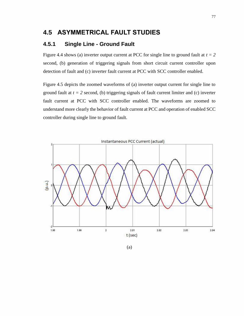
77
4.5 ASYMMETRICAL FAULT STUDIES
4.5.1 Single Line - Ground Fault
Figure 4.4 shows (a) inverter output current at PCC for single line to ground fault at t = 2
second, (b) generation of triggering signals from short circuit current controller upon
detection of fault and (c) inverter fault current at PCC with SCC controller enabled.
Figure 4.5 depicts the zoomed waveforms of (a) inverter output current for single line to
ground fault at t = 2 second, (b) triggering signals of fault current limiter and (c) inverter
fault current at PCC with SCC controller enabled. The waveforms are zoomed to
understand more clearly the behavior of fault current at PCC and operation of enabled SCC
controller during single line to ground fault.
(a)

78
(b)
(c)
Figure 4.4: (a) Inverter Fault Current at t = 2 sec. (b) Triggering Signals (c)
Inverter Fault Current with SCC Controller

79
(a)
(b)
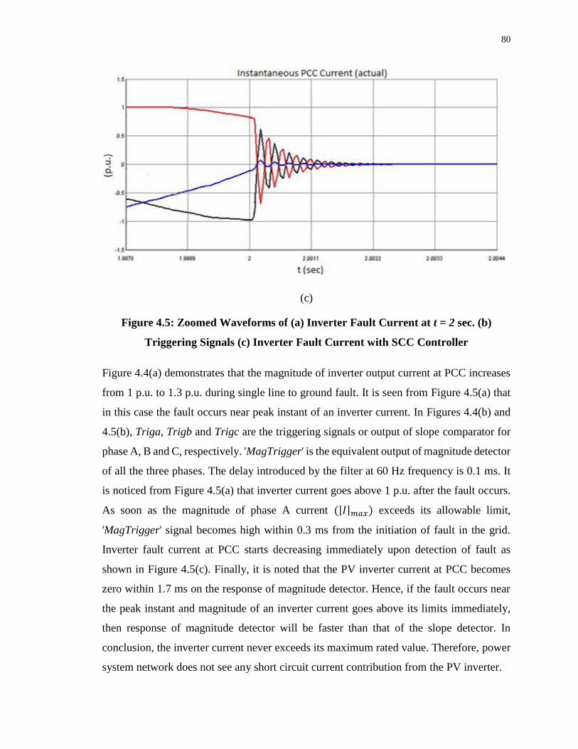
80
(c)
Figure 4.5: Zoomed Waveforms of (a) Inverter Fault Current at t = 2 sec. (b)
Triggering Signals (c) Inverter Fault Current with SCC Controller
Figure 4.4(a) demonstrates that the magnitude of inverter output current at PCC increases
from 1 p.u. to 1.3 p.u. during single line to ground fault. It is seen from Figure 4.5(a) that
in this case the fault occurs near peak instant of an inverter current. In Figures 4.4(b) and
4.5(b), Triga, Trigb and Trigc are the triggering signals or output of slope comparator for
phase A, B and C, respectively. 'MagTrigger' is the equivalent output of magnitude detector
of all the three phases. The delay introduced by the filter at 60 Hz frequency is 0.1 ms. It
is noticed from Figure 4.5(a) that inverter current goes above 1 p.u. after the fault occurs.
As soon as the magnitude of phase A current (|𝐼|𝑚𝑎𝑥) exceeds its allowable limit,
'MagTrigger' signal becomes high within 0.3 ms from the initiation of fault in the grid.
Inverter fault current at PCC starts decreasing immediately upon detection of fault as
shown in Figure 4.5(c). Finally, it is noted that the PV inverter current at PCC becomes
zero within 1.7 ms on the response of magnitude detector. Hence, if the fault occurs near
the peak instant and magnitude of an inverter current goes above its limits immediately,
then response of magnitude detector will be faster than that of the slope detector. In
conclusion, the inverter current never exceeds its maximum rated value. Therefore, power
system network does not see any short circuit current contribution from the PV inverter.

81
4.5.2 Line - Line Fault
Figure 4.6 showcases (a) inverter output current at PCC for LL fault at t = 2 second, (b)
generation of triggering signals (Triga, Trigb, Trigc and MagTrigger) from SCC controller
upon detection of fault and (c) inverter fault current with short circuit current controller
enabled.
To better understand the behavior of fault current at PCC and operation of enabled short
circuit current controller during LL fault, Figure 4.7 illustrates the zoomed waveforms of
(a) inverter output current for LL fault at t = 2 second with SCC controller disabled, (b)
triggering signals from SCC controller and (c) inverter fault current at PCC with SCC
controller enabled.
(a)

82
(b)
(c)
Figure 4.6: (a) Inverter Fault Current at t = 2 sec. (b) Triggering Signals (c)
Inverter Fault Current with SCC Controller

83
(a)
(b)

84
(c)
Figure 4.7: Zoomed Waveforms of (a) Inverter Fault Current at t = 2 sec. (b)
Triggering Signals (c) Inverter Fault Current with SCC Controller
Figure 4.6(a) shows that the magnitude of inverter output current at PCC reaches up to 2
p.u. The large transients or distortion of the faulted current waveform can be seen in Figure
4.7(a) after the inception of fault from t = 2 second. It is observed from Figure 4.7(b) that
with the SCC controller enabled, ‘Trigb’ signal becomes high in 0.2 ms from the initiation
of fault at t = 2 second. Phase B has violated the maximum permissible limits of rate
limiter (𝑑𝑖
𝑑𝑡), so 'Trigb' signal rises from 0 to 1. Slope detector responds instantly before the
current exceeds its peak rated value. 'Trigb' signal is given to gating signals of a PV
inverter, solar farm and AC filter capacitor. PV solar farm modules stop transferring current
to the grid within 1.6 ms from the initiation of fault in the grid as shown in Figure 4.7(c).
It is also noticed from Figure 4.7(c), that the current does not exceed its maximum rated
value i.e. 1 p.u.
4.5.3 Line - Line - Ground Fault
The behavior of inverter output current during LLG fault at t = 2 second is found to be
identical to LL fault case (Section 4.5.2). The operation of the short circuit current

85
controller will therefore be the same for both these types of fault cases. Hence, the
simulation results will be same as described in Section 4.5.2. and are not repeated here.
4.6 SYMMETRICAL FAULT STUDIES
4.6.1 Line - Line - Line Fault
Figure 4.8 depicts (a) Inverter fault current at PCC for LLL fault at t = 2 second with SCC
controller disabled, (b) triggering signals (Triga, Trigb, Trigc and MagTrigger) of fault
current limiter upon detection of fault and (c) inverter fault current at PCC with SCC
controller enabled.
Figure 4.9 represents the zoomed waveforms of (a) inverter output current at PCC for LLL
fault at t = 2 second with SCC controller disabled, (b) triggering signals of fault current
limiter upon detection of fault and (c) inverter fault current at PCC with SCC controller
enabled. These waveforms are zoomed to understand more precisely the behavior of fault
current at PCC and operation of enabled fault current controller during LLL fault.
(a)

86
(b)
(c)
Figure 4.8: (a) Inverter Fault Current at t = 2 sec. (b) Triggering Signals (c)
Inverter Fault Current with SCC Controller

87
(a)
(b)

88
(c)
Figure 4.9: Zoomed Waveforms of (a) Inverter Fault Current at t = 2 sec. (b)
Triggering Signals (c) Inverter Fault Current with SCC Controller
LLL fault is a symmetrical fault which occurs rarely in a transmission line but can
potentially cause a severe damage on occurrence. Figure 4.8(a) demonstrates that the
magnitude of inverter output current at PCC during symmetrical fault increases till 2 p.u.
In Figures 4.8(b) and 4.9(b), Triga, Trigb and Trigc are the triggering signals or output of
slope comparator for phase A, B and C, respectively. 'MagTrigger' is the equivalent output
of magnitude detector of all the three phases. It is noticed from Figure 4.9(b) that 'Triga'
signal has become high after 0.1 ms from the initiation of fault in the grid, as slope of phase
A (𝑑𝑖
𝑑𝑡) has gone beyond its permissible limits. Later, MagTrigger and other triggering
signals violate their limits. However, the salient feature of the SCC controller is that only
one triggering signal is needed to disconnect the PV inverter from the grid. Finally from
Figure 4.9(c), it is concluded that magnitude of inverter output current at PCC becomes
zero in 1.5 ms after the fault occurs. This means that no short circuit current gets transferred
from PV inverter to the grid. In addition, inverter current does not exceed its maximum
rated value. Therefore, power system network does not see any short circuit current
contribution from PV inverter.

89
4.6.2 Line - Line - Line - Ground Fault
Figure 4.10 shows (a) inverter output current at PCC for LLLG fault at t = 2 second, (b)
generation of triggering signals (Triga, Trigb, Trigc and MagTrigger) from SCC controller
upon detection of fault and (c) inverter fault current at PCC with short circuit current
controller enabled.
(a)
(b)

90
(c)
Figure 4.10: (a) Inverter Fault Current at t = 2 sec. (b) Triggering Signals (c)
Inverter Fault Current with SCC Controller
(a)

91
(b)
(c)
Figure 4.11: Zoomed Waveforms of (a) Inverter Fault Current at t = 2 sec. (b)
Triggering Signals (c) Inverter Fault Current with SCC Controller
To better understand the behavior of fault current at PCC and operation of enabled short
circuit current controller during LLLG fault, Figure 4.11 illustrates the zoomed waveforms
of (a) inverter output current for LLLG fault at t = 2 second with SCC controller disabled,

92
(b) triggering signals of fault current limiter and (c) inverter fault current at PCC with SCC
controller enabled.
Figure 4.10(a) exhibits that the magnitude of inverter output current at PCC rises from 1
p.u. to 1.95 p.u when LLLG fault occurs in grid. Large transients or distortion of the faulted
current waveform are seen in Figure 4.11(a) after the inception of fault from t = 2 second.
It is observed in Figure 4.11(b) that with the SCC controller enabled, 'Triga' signal becomes
high in 0.3 ms from the initiation of fault at t = 2 second. Phase A has violated the maximum
permissible limits of rate limiter (𝑑𝑖
𝑑𝑡), so 'Triga' signal rises from 0 to 1. Slope detector
responds quickly before the current exceeds peak rated value. PV inverter is disconnected
completely from the grid within 1.7 ms from the initiation of fault in the grid as shown in
Figure 4.11(c) without the inverter current exceeding its rated value.
4.7 FAULT STUDIES AT DIFFERENT TIME INSTANTS
Fault studies are also performed by applying different types of faults at different time
instants to ensure that controller will respond in the expected manner regardless of any type
of fault at any time instant. The simulation results are shown below.
4.7.1 Asymmetrical Fault
Figure 4.12 shows (a) Inverter fault current at PCC for LLG fault at t = 5.0018 second with
SCC controller disabled, (b) generation of triggering signals (Triga, Trigb, Trigc and
MagTrigger) of fault current limiter upon detection of fault and (c) inverter fault current at
PCC with SCC controller enabled. Figure 4.12(a) demonstrates that the LLG fault occurs
between the zero crossing and close to current peak for both phase A and B.

93
(a)
(b)

94
(c)
Figure 4.12: (a) Inverter Fault Current at t = 5.0018 sec. (b) Triggering Signals
(c) Inverter Fault Current with SCC Controller
(a)

95
(b)
(c)
Figure 4.13: Zoomed Waveforms of (a) Inverter Fault Current at t = 5.0018 sec.
(b) Triggering Signals (c) Inverter Fault Current with SCC Controller
To clearly understand the behavior of fault current at PCC and operation of enabled fault
current controller during LLG fault, Figure 4.13 illustrates the zoomed waveforms of (a)
inverter output current for LLG fault at t = 5.0018 second with SCC controller disabled,

96
(b) triggering signals of fault current limiter and (c) inverter fault current at PCC with SCC
controller enabled.
Figure 4.12(a) demonstrates that the magnitude of inverter output current at PCC during
LLG fault rises till 1.95 p.u. Large transients are observed in Figure 4.13(a) from the
initiation of fault at t = 5.0018 second. It is noticed from Figure 4.13(b) that 'Triga' signal
becomes high within 0.2 ms from the initiation of fault in the grid, as slope of phase A (𝑑𝑖
𝑑𝑡)
has exceeded its maximum allowable limits. Later, MagTrigger and other triggering signals
get high. As soon as the 'Triga' signal becomes high, inverter fault current at PCC starts
decreasing as shown in Figure 4.13(c). Finally, it is concluded from Figure 4.13(c) that
instantaneous current at PCC becomes zero within 1.6 ms upon the response of slope
detector. This means that no current gets transferred from PV inverter to the grid. In
addition, inverter current does not exceed its maximum value. Therefore, the power system
network does not see any short circuit current contribution from PV inverter.
4.7.2 Symmetrical Fault
Figure 4.14 demonstrates (a) inverter output current at PCC for LLL fault at t = 3.5077
second, (b) generation of triggering signals (Triga, Trigb, Trigc and MagTrigger) from
SCC controller upon detection of fault and (c) inverter fault current at PCC with short
circuit current controller enabled. The symmetrical fault occurs above the positive going
zero crossing of phase A, close to the peak current of phase B, and near negative going
zero crossing of phase C.
Figure 4.15 depicts the zoomed waveforms of (a) inverter output current at PCC for LLLG
fault at t = 3.5077 second, (b) triggering signals of fault current limiter and (c) inverter
fault current at PCC with SCC controller enabled. The waveforms are zoomed to
understand more clearly the behavior of fault current at PCC and operation of the SCC
controller during single line to ground fault.

97
(a)
(b)

98
(c)
Figure 4.14: (a) Inverter Fault Current at t = 3.5077 sec. (b) Triggering Signals
(c) Inverter Fault Current with SCC Controller
(a)

99
(b)
(c)
Figure 4.15: Zoomed Waveforms of (a) Inverter Fault Current at t = 3.5077 sec.
(b) Triggering Signals (c) Inverter Fault Current with SCC Controller
Figure 4.14(a) shows that the magnitude of inverter output current at PCC reaches up to 2
p.u. Large transients or distortion of the faulted current waveform are seen in Figure 4.15(a)
after the inception of fault from t = 3.5077 second. It is observed in Figure 4.15(b) that
with the SCC controller enabled, 'Trigb' signal becomes high in 0.2 ms from the initiation

100
of fault. Phase B has violated the maximum permissible limits of rate limiter (𝑑𝑖
𝑑𝑡), so 'Trigb'
signal rises from 0 to 1. 'Trigb' signal is given to the gating signals of a PV inverter, solar
farm and AC filter capacitor. At t = 3.5095 sec, instantaneous current at PCC goes to almost
zero as shown in Figure 4.15(c). Thus, PV inverter is disconnected from the grid within 1.8
ms from the point of fault inception without exceeding the maximum rated value of current.
Hence, the SCC controller is successful in disconnecting the PV inverter from the grid
regardless of any type of fault or location of fault on the distribution system, which can
possibly cause short circuit current to exceed the rated inverter current.
4.8 LOAD SWITCHING
Figure 4.16(a) depicts the PV inverter output current for a load switching event for a time
instant at t = 5.0035 second. Figure 4.16(b) demonstrates the triggering signals for the short
circuit current controller enabled. It is observed that the enabled controller does not respond
to a load switching event of a large feeder load of 60 MW. The steep rate of change in
current during the load switching is considered as the slope of high frequency spike which
does not last long. These spikes will be removed by low pass filter (Fig.3.2).
(a)

101
(b)
Figure 4.16: (a) PV Inverter Current with 60 MW, 0.9 pf. Load Switching (b)
Triggering Signals from SCC Controller
If the spikes are not cleared even after filtering then the intentional time delay of 10 µs
introduced in the clock of D flip-flop will take care of this transient event as described in
Section 2.3.2 and 3.3. Hence a false triggering is avoided at this switching event. This
ensures the effectiveness of SCC controller during load switching events
4.9 COMPARISON BETWEEN RTDS AND PSCAD RESULTS
The similarities and differences of RTDS and PSCAD simulation results are as follows:
Similarities: The performance of SCC controller in RTDS is seen to be similar to that of
PSCAD simulation results. The SCC controller successfully shuts off the PV inverter in
maximum of 2 ms from the initiation of fault in the grid for all asymmetrical (SLG, LL,
and LLG) and symmetrical (LLL, LLLG) fault cases without exceeding maximum rated
value of current.

102
Differences: For LL and LLL fault case studies, RTDS results (Fig. 4.6(a) and 4.8(a)) show
larges transients during fault condition as compared to PSCAD simulation results (Fig.
3.5(a) and 3.7(a)). The magnitude of inverter current during LL and LLL fault increases
upto 2 p.u. in RTDS. While in PSCAD, magnitude of inverter current reaches 1.45 p.u.
This is because, component models (inductor, capacitor, etc.) in RTDS are programmed
differently than in PSCAD. Therefore, the behavior of inverter current during short circuit
scenario will not be same.
Another difference is when the SCC controller shuts off the PV inverter through GTO
switches, inverter current in RTDS decreases immediately on detection of fault but
continues to oscillate for few milliseconds and then settles to zero. While in PSCAD,
inverter current decreases gradually and settles to zero without oscillating. However, this
entire process takes place within 2 ms for both RTDS and PSCAD simulation results.
Nevertheless, RTDS results seem to be more realistic and accurate compared to PSCAD
simulation results. Overall, the PSCAD results are considered to be validated with RTDS.
4.10 CONCLUSION
In this chapter, performance of short circuit current controller is validated on a Real Time
Digital Simulator (RTDS). Such a testing is typically performed in the final stages of
controller validation by commercial equipment manufacturers. The SCC controller is based
on the slope (𝑑𝑖
𝑑𝑡) and magnitude |𝐼| of the PV inverter output current computation. The
studies are performed on the model of a typical distribution of Ontario, Canada. Following
conclusions are drawn.
Studies are performed for different types of asymmetrical faults - SLG, LL, and
LLG fault, with the SCC controller enabled. PV inverter is disconnected form the
grid within maximum 1.7 ms from the initiation of fault in the grid without
exceeding the maximum rated value. For majority of the cases, triggering signal is
generated on the response of slope detector (𝑑𝑖
𝑑𝑡).

103
Symmetrical faults such as LLL and LLLG faults are applied on the point of
common coupling (PCC) with the SCC controller enabled. PV solar farm modules
stop transferring current to the grid within maximum of 1.6 ms from the initiation
of fault in the grid without exceeding maximum permissible limits. In these case
studies, slope detector (𝑑𝑖
𝑑𝑡) responds faster than the magnitude detector on the
detection of fault.
Different types of fault are applied on PCC at different time instants to ensure the
effectiveness of SCC controller. Both asymmetrical and symmetrical fault occurs
between the zero crossing and peak instant of the current, hence, slope detector
generates triggering signal upon detection of the fault. The PV inverter current is
limited in maximum of 1.8 ms on the response of slope detector.
The SCC controller is shown to effectively distinguish between large load
switching and fault current. Therefore, the generation of undesired tripping signal
is avoided.
Hence, real time simulation studies using RTDS has proved that the short circuit current
controller disconnects the PV inverter from the grid within 2 milliseconds regardless of
any type of fault or location of fault on the distribution system. Hence, PV inverter does
not contribute any short circuit current to the grid.

104
CHAPTER 5
VALIDATION OF SHORT CIRCUIT CURRENT CONTROLLER ON dSPACE
5.1 INTRODUCTION
This chapter presents the hardware implementation of the short circuit current controller
on the dSPACE controller board. The performance of the SCC controller is subsequently
validated on dSPACE controller board with actual PV inverter short circuit waveforms
obtained from Southern California Edison Short Circuit Testing Lab. The hardware of the
SCC controller is developed with TMS320F28335 eZdsp board and various interfacing
circuits. The generation of triggering signals from controller is monitored for different fault
conditions. The performance of SCC controller is monitored and validated for the desired
operation utilizing ScopeCorder Yokogawa DL850E.
Section 5.2 briefs about the concept of dSPACE; Section 5.3 gives an overview on the
dSPACE platform; Section 5.4 represents the generation of transients from PV inverter
current waveforms obtained from SCE lab; Section 5.5 depicts the implementation of SCC
controller on dSPACE board; and Section 5.6 illustrates the dSPACE test results. The
actual implementation of short circuit current controller is explained in Section 5.7. Finally,
the outcome of this work is concluded in Section 5.8.
5.2 CONCEPT OF dSPACE SIMULATION
For rapid prototype developments, different types of real time controller platforms are used
such as dSPACE [70], National Instruments [71] and xPC targets [72]. dSPACE is used
extensively in several industrial applications due to its various advantages such as
visualization tools, different hardware and extensive array of software options [73,74].
Hence, dSPACE platform is used here for the validation of SCC controller.
The SCC controller is designed in MATLAB/Simulink environment. Then, it is
transformed on to the dSPACE controller board through Real Time Interface (RTI)

105
libraries available in Simulink to perform real time simulations. The SCE lab results are
sampled at a rate of 50 µs and subsequently passed through the controller. dSPACE reads
these signals and performs appropriate control actions to generate a triggering signal to
shut down / disconnect the inverter, AC filter capacitor and solar panels.
5.3 OVERVIEW OF dSPACE PLATFORM
5.3.1 dSPACE Software
Simulink Coder PPC CompilerMATLAB/Simulink
Real Time Interface Library
Control DeskMLIB/MTRACE
Device Driver
dSPACE Hardware Board
.mdl .c
.ppc
Workstation Environment
dSPACE System
Software
Hardware
Real-Time Data
.mdl, .c and .ppc are output file format
#
Figure 5.1: Block Diagram of dSPACE Software System
Figure 5.1 describes about the block diagram of dSPACE software system. The SCC
controller is modeled in MATLAB/Simulink with the help of different components
available in its library. The simulink model (.mdl file) is transformed into custom C code
by Simulink coder specific to the dSPACE controller board. PPC compiler combines this
developed C code with RTI libraries which executes the developed model on the dSPACE
controller board using the MATLAB library functions MLIB/MTRACE. RTI libraries
provide Simulink/dSPACE blocks as well as an input/output interface between Simulink
and the dSPACE controller. This will enable a model to run in a specific dSPACE hardware
platform. Control Desk is a Graphical User Interface (GUI) software which is used to
monitor the program variables during the run time of the simulation. An interface to access

106
the dSPACE controller board from the Control Desk software or MATLAB/Simulink
environment is provided by device driver. The detailed software architecture is provided
in the dSPACE software manual [70].
5.3.2 dSPACE Controller Board
Figure 5.2 demonstrates the dSPACE controller hardware subsystems. The dSPACE
controller board consists of DS1103 controller board, CLP1103 connector panel and link
boards - DS814 and DS817 to communicate between host PC and the PX4 expansion box.
Ethernet crossover cable is used to connect the host PC or computer work station to
dSPACE controller board. The detailed hardware architecture is outlined in the dSPACE
hardware manual [70].
Host PC PX4 Expansion Box
DS814 Link BoardDS817 Link Board
Control Desk
MATLAB/Simulink
DS1103 Controller Card
CLP 1103 Connector Panel CLP 1103 Connector Panel
Power Supply
Unit
Analog Digital Interface
Ethernet Cable
Adapter Cables
LED
LED
Figure 5.2: Block Diagram of dSPACE Hardware System
5.3.2.1 PX4 Expansion Box
A PX4 expansion box houses the power supply units, DS1103 controller board and DS814
link board.

107
5.3.2.2 DS1103 Controller Board
DS1103 controller board is an essential part of the dSPACE system where the SCC
controller runs. This board is comprised of two types of controllers: Master and Slave
controller. The master controller is a Motorola Power PC (PPC) processor running at a
clock rate of 333MHz. The slave controller is a Texas instrument based on Digital Signal
Processor (DSP) microcontroller TMS320F240 operating at a clock rate of 20MHz.
5.3.2.3 CLP1103 Connector Panel
The CLP1103 controller panel features the input and output signals to access I/O units of
DS11103 controller board. The connector panel is equipped with BNC (Bayonet Neill–
Concelman) connectors to access analog and digital signals. Similarly, sub-D connectors are
used to provide connections for the interface signals.
5.3.2.4 DS814 Link Board
The DS814 is an Industry Standard Architecture (ISA) bus interface card which is used to
communicate between the DS1103 controller board and the DS817 card installed in the PC.
This link board is installed in PX4 expansion box.
5.3.2.5 DS817 Link Board
The DS817 link board is used to communicate between the PC and the DS814 link board
installed in the PX4 expansion box. It is an interface card installed in the PC.
5.4 ANALYSIS OF ACTUAL SHORT CIRCUIT CURRENT WAVEFORMS
The real time data for commercial PV inverters during asymmetrical - SLG, LL and LLG
faults are obtained from Southern California Edison (SCE) lab. All the faults are noted to
occur at different time instants. Upon examination, it is found out that the short circuit
current waveforms include many transients. To examine the transients, a Fast Fourier
Transform (FFT) is performed on all the obtained SCE lab results.
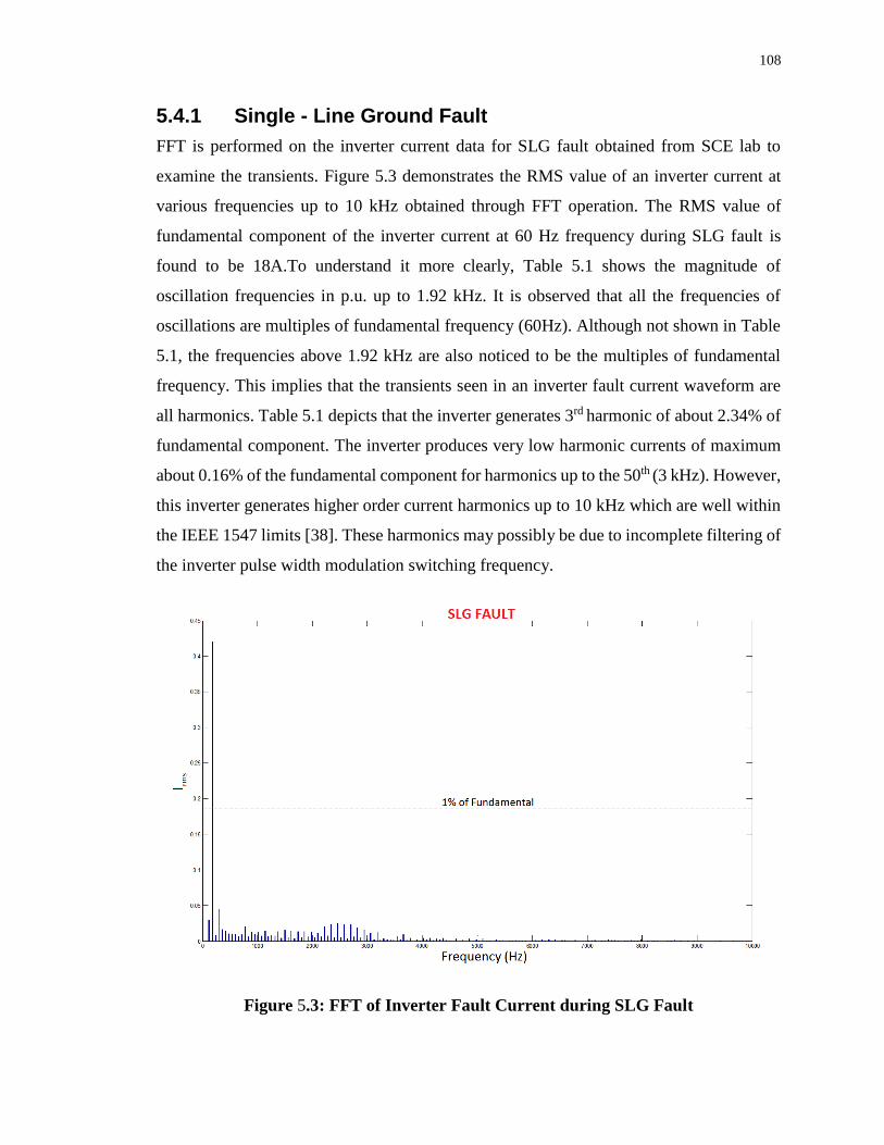
108
5.4.1 Single - Line Ground Fault
FFT is performed on the inverter current data for SLG fault obtained from SCE lab to
examine the transients. Figure 5.3 demonstrates the RMS value of an inverter current at
various frequencies up to 10 kHz obtained through FFT operation. The RMS value of
fundamental component of the inverter current at 60 Hz frequency during SLG fault is
found to be 18A.To understand it more clearly, Table 5.1 shows the magnitude of
oscillation frequencies in p.u. up to 1.92 kHz. It is observed that all the frequencies of
oscillations are multiples of fundamental frequency (60Hz). Although not shown in Table
5.1, the frequencies above 1.92 kHz are also noticed to be the multiples of fundamental
frequency. This implies that the transients seen in an inverter fault current waveform are
all harmonics. Table 5.1 depicts that the inverter generates 3rd harmonic of about 2.34% of
fundamental component. The inverter produces very low harmonic currents of maximum
about 0.16% of the fundamental component for harmonics up to the 50th (3 kHz). However,
this inverter generates higher order current harmonics up to 10 kHz which are well within
the IEEE 1547 limits [38]. These harmonics may possibly be due to incomplete filtering of
the inverter pulse width modulation switching frequency.
Figure 5.3: FFT of Inverter Fault Current during SLG Fault

109
No. Oscillation
Frequency
(Hz)
Harmonic
Order
Mag
(p.u.)
17. 1020 17th 0.00062
18. 1080 18th 0.00041
19. 1140 19th 0.0020
20. 1200 20th 0.00032
21. 1260 21st 0.00044
22. 1320 22nd 0.00039
23. 1380 23ed 0.0007
24. 1440 24th 0.0040
25. 1500 25th 0.00083
26. 1560 26th 0.00024
27. 1620 27th 0.0008
28. 1680 28th 0.00022
29. 1740 29th 0.0001
30. 1800 30th 0.0007
31. 1860 31st 0.0002
32. 1920 32nd 0.00033
No. Oscillation
Frequency
(Hz)
Harmonic
Order
Mag
(p.u.)
1. DC - 0.0011
2. 120 2nd 0.0016
3. 180 3rd 0.0234
4. 240 4th 0.0004
5. 300 5th 0.0025
6. 360 6th 0.0009
7. 420 7th 0.0007
8. 480 8th 0.0006
9. 540 9th 0.00053
10. 600 10th 0.00054
11. 660 11th 0.0003
12. 720 12th 0.00055
13. 780 13th 0.0011
14. 840 14th 0.0003
15. 900 15th 0.0007
16. 960 16th 0.00051
Ibase= 18A
Table 5.1: Oscillation Frequencies of the Inverter Current during SLG Fault
Ibase = 18 A

110
5.4.2 Line - Line Fault
FFT is now performed on the inverter current data for LL fault obtained from SCE lab to
investigate the transients. Figure 5.4 depicts the result of an FFT operation of an inverter
current for various frequencies up to 10 kHz. The RMS value of fundamental component
of an inverter current at 60 Hz frequency during SLG fault is 11 A. To understand it more
precisely, Table 5.2 shows the magnitude of oscillation frequencies in p.u. up to 1.92 kHz.
It is observed that all the frequencies of oscillations are multiples of fundamental frequency
(60Hz). Although not shown in Table 5.2, the frequencies above 1.92 kHz are also found
to be the multiples of fundamental frequency. This implies that the transients seen in an
inverter fault current waveform are all harmonics. It can be observed from Table 5.2 that
inverter generates 3rd harmonic current of 2.34% of the fundamental component. Inverter
produces very low harmonic currents of maximum about 0.41% of the fundamental
component on harmonics up to the 50th (3 kHz). The inverter further generates higher order
current harmonics up to 10 kHz which are less than the IEEE 1547 Standard limits [38].
Figure 5.4: FFT of Inverter Fault Current during LL Fault

111
No. Oscillation
Frequency
(Hz)
Harmonic
Order
Mag
(p.u.)
17. 1020 17th 0.0008
18. 1080 18th 0.0003
19. 1140 19th 0.00062
20. 1200 20th 0.00036
21. 1260 21st 0.00076
22. 1320 22nd 0.00044
23. 1380 23ed 0.00078
24. 1440 24th 0.0003
25. 1500 25th 0.00077
26. 1560 26th 0.00031
27. 1620 27th 0.00072
28. 1680 28th 0.00029
29. 1740 29th 0.00041
30. 1800 30th 0.0009
31. 1860 31st 0.0011
32. 1920 32nd 0.00038
No. Oscillation
Frequency
(Hz)
Harmonic
Order
Mag
(p.u.)
1. DC - 0.0020
2. 120 2nd 0.0008
3. 180 3rd 0.0234
4. 240 4th 0.00003
5. 300 5th 0.0041
6. 360 6th 0.0012
7. 420 7th 0.0009
8. 480 8th 0.0006
9. 540 9th 0.0005
10. 600 10th 0.00061
11. 660 11th 0.0007
12. 720 12th 0.00052
13. 780 13th 0.00071
14. 840 14th 0.00053
15. 900 15th 0.0009
16. 960 16th 0.00053
Ibase = 11 A
Table 5.2: Oscillation Frequencies of the Inverter Current during LL Fault

112
5.4.3 Line - Line - Ground Fault
Figure 5.5 represents the result of the FFT operation on the inverter current during LLG
fault to examine the transients in the inverter fault current waveform. Figure 5.5 shows the
RMS value of an inverter current at various frequencies up to 10 kHz. The RMS value of
fundamental component of an inverter current at 60 Hz frequency during SLG fault is 15
A. Table 5.3 shows the magnitude of oscillation frequencies in p.u. up to 1.92 kHz. It is
observed that all frequencies of oscillations are multiples of fundamental frequency
(60Hz). Although not shown in Table 5.3, the frequencies above 1.92 kHz are also found
to be the multiples of fundamental frequency. This confirms that the transients seen in an
inverter fault current waveform are harmonics. It can be observed from Table 5.3 that
inverter generates 3rd harmonic current of 2.34% of the fundamental component. The
inverter produces very low harmonic currents of maximum about 0.37% of the fundamental
component for harmonics up to the 50th (3 kHz). The inverter generates higher order current
harmonics up to 10 kHz which are once again below the IEEE 1547 Standard limits [38].
Figure 5.5: FFT of Inverter Fault Current during LLG Fault

113
No. Oscillation
Frequency
(Hz)
Harmonic
Order
Mag
(p.u.)
17. 1020 17th 0.00083
18. 1080 18th 0.0004
19. 1140 19th 0.00063
20. 1200 20th 0.00044
21. 1260 21st 0.00065
22. 1320 22nd 0.00036
23. 1380 23ed 0.00088
24. 1440 24th 0.00038
25. 1500 25th 0.0008
26. 1560 26th 0.0003
27. 1620 27th 0.0008
28. 1680 28th 0.00035
29. 1740 29th 0.00083
30. 1800 30th 0.0004
31. 1860 31st 0.0007
32. 1920 32nd 0.0003
No. Oscillation
Frequency
(Hz)
Harmonic
Order
Mag
(p.u.)
1. DC - 0.0009
2. 120 2nd 0.0016
3. 180 3rd 0.0234
4. 240 4th 0.00032
5. 300 5th 0.0037
6. 360 6th 0.0011
7. 420 7th 0.0008
8. 480 8th 0.00052
9. 540 9th 0.0002
10. 600 10th 0.0007
11. 660 11th 0.0005
12. 720 12th 0.00055
13. 780 13th 0.00086
14. 840 14th 0.00058
15. 900 15th 0.0009
16. 960 16th 0.0004
Ibase = 15 A
Table 5.3: Oscillation Frequencies of the Inverter Current during LLG Fault

114
5.5 IMPLEMENTATION OF SCC CONTROLLER ON dSPACE BOARD
Figure 5.6 depicts the implementation of the short circuit current controller on dSPACE
board. The Simulink software environment along with MATLAB-dSPACE block sets are used
to develop SCC controller. RTI1103 and Simulink libraries contain real time library interface
block sets. These libraries get initialized in the Simulink software once MATLAB starts
running [57].
The SCE lab results for commercial inverters are available in MATLAB workspace. This
discrete data is transferred to Simulink environment with a block called “From Workspace”
available in Simulink library. The input signals are discretized at a sample rate of 50 µs.
The input signals contain harmonics as described in Section 5.4. Therefore, a digital filter
is designed to remove these harmonics. The critical issue while designing the filter is the
delay introduced by it. The designed filter should introduce minimum delay with a good
filtering performance for the short circuit current controller to respond in 1-2 ms during
short circuit scenarios. Group delay can be reduced by increasing cut off frequency at same
sampling frequency but the performance of the filter will be poor. So there is a tradeoff
between cutoff frequency and filter performance. Therefore, a discrete 4th Order IIR
(Infinite Impulse Response) Low Pass Butterworth filter [91] has been designed. The
sampling and cut-off frequency of the filter are chosen as 20 kHz and 500 Hz, respectively.
A Butterworth filter has been chosen due to its several characteristics such as maximally
flat magnitude response in the pass band, step response having moderate overshoot and
ringing lower than Chebyshev filter, and rate of attenuation better than Bessel filter [92].
The main advantage of Butterworth filter is that it eliminates the noise without affecting
the amplitude of input signal. With the help of filter visualization tool in MATLAB, group
delay response of the designed filter is plotted. Figure 5.7 illustrates the group delay
introduced by the designed filter at various frequencies. IIR filter is a frequency dependent
delay filter. Therefore, filter delay will not be constant. Filter gives a delay of 0.83 ms at
60 Hz frequency as shown in Figure 5.7. Thereafter, the input signals are passed through
the digital filter using Simulink block sets.

115
Figure 5.6: Implementation of SCC Controller on dSPACE

116
Figure 5.7: Filter Delay
After a time delay of 1 second, the inputs are passed through slope and magnitude
comparators. These modules and their operations are already discussed in Section 2.3.2
and 3.3. The parameters for magnitude and slope comparators are 32.0A and 12060
amperes per second, respectively. The output of the SCC controller as modeled in Simulink
is the 'Trip' signal. This output signal is then given to dSPACE DAC channel. The DAC
channel converts Simulink output in the range of -10 to 10 volts. Therefore, 'Trip' signal in
Simulink is multiplied with a gain of 0.1 to get the same output signal from DAC channel.
Figure 5.8 shows the dSPACE test set up to analyze the performance of short circuit current
controller. The DAC channel from dSPACE board is connected to Yokogawa DL850E via
BNC connectors to examine the output signal as shown in Figure 5.8. This DL850E
ScopeCorder is a powerful portable data acquisition recorder and oscilloscope that can
capture and analyze transient events. It is able to trigger on electrical power related and
other calculations in real time. Similarly, the input discrete signals are multiplied with gain
of 0.1 and corresponding DAC channels are assigned. Simulink model (.mdl file) is
transformed into a custom C code (.sdf file) by Simulink coder specific to the dSPACE
controller board on compilation. Thereafter, .sdf file is loaded into Control Desk software.

117
Once the software starts running, the input and output signals connected to Yokogawa are
analyzed to understand the performance of the short circuit current controller.
dSPACE Hardware
Figure 5.8: dSPACE Test Set Up
5.6 dSPACE RESULTS
SCE lab data of PV inverter current during asymmetrical faults at different time instants
are passed through the short circuit current controller implemented on dSPACE board,
which is further connected to Yokogawa DL850E [95]. The peak rated value of an inverter
current for all the fault cases is 32.0A. To understand the performance of the SCC controller
more precisely, the results are extracted from Yokogawa and plotted in MATLAB. The test
results are shown below.

118
5.6.1 Single Line - Ground Fault
Figure 5.9 represents the performance of short circuit current controller on dSPACE board
during SLG fault. Figure 5.9 depicts (a) original inverter current during SLG fault, (b)
filtered inverter fault current, (c) generation of triggering signal from SCC controller and
(d) inverter fault current with SCC controller enabled. Figure 5.10 shows the validation
results of SCC controller in Yokogawa for SLG fault.
According to SCE lab data, PV inverter current increases up to 1.34 p.u. during SLG fault
as demonstrated in Figure 5.9(a). Here, the fault occurs at t = 6.8194 second near zero
crossing. The impedance and location of fault is not known. The original short circuit
current waveform is filtered with 4th order IIR Low Pass Butterworth filter as seen in Figure
5.9(b). The filter introduces a delay of 0.83 ms at 60 Hz frequency. Therefore, controller
can sense the short circuit condition only after 0.83 ms of its occurrence due to filter delay.
It is noticed from Figure 5.9(b) that the slope of the current waveform increases when SLG
fault occurs. Therefore, the triggering signal is generated by the SCC controller upon the
detection of fault as illustrated in Figure 5.9(c). The triggering signal goes high on the
response of slope detector (𝑑𝑖
𝑑𝑡) as slope of phase B (black waveform) has exceeded its
maximum allowable limits. The inverter current is inhibited as soon as the triggering signal
goes high. It goes to zero at t = 6.8207 second as shown in Figure 5.9(d). This means that
SCC controller takes 1.3 ms to limit the PV inverter current without exceeding the peak
rated value or 1 p.u.
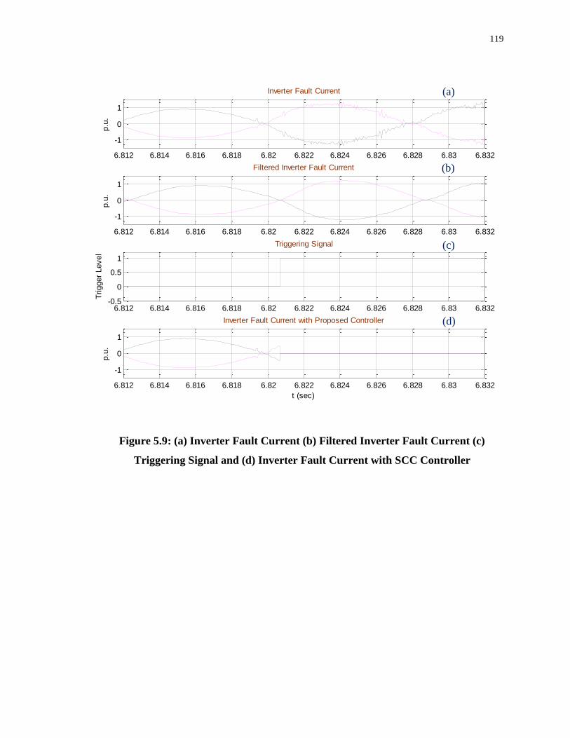
119
Figure 5.9: (a) Inverter Fault Current (b) Filtered Inverter Fault Current (c)
Triggering Signal and (d) Inverter Fault Current with SCC Controller
6.812 6.814 6.816 6.818 6.82 6.822 6.824 6.826 6.828 6.83 6.832
-1
0
1
Inverter Fault Current
p.u
.
6.812 6.814 6.816 6.818 6.82 6.822 6.824 6.826 6.828 6.83 6.832
-1
0
1
Filtered Inverter Fault Current
p.u
.
6.812 6.814 6.816 6.818 6.82 6.822 6.824 6.826 6.828 6.83 6.832-0.5
0
0.5
1
Triggering Signal
Trigger
Level
6.812 6.814 6.816 6.818 6.82 6.822 6.824 6.826 6.828 6.83 6.832
-1
0
1
Inverter Fault Current with Proposed Controller
p.u
.
t (sec)
(a)
(b)
(c)
(d)

120
Figure 5.10: Performance of SCC Controller in Yokogawa during SLG Fault

121
5.6.2 Line - Line Fault
Figure 5.11 presents (a) original inverter current during LL fault, (b) filtered inverter fault
current, (c) generation of triggering signal from SCC controller and (d) inverter fault
current with SCC controller enabled. Figure 5.12 demonstrates the snapshot of validation
results of SCC controller in Yokogawa when LL fault occurs.
Figure 5.11(a) demonstrates that the PV inverter current rises from 1 p.u. to 2.2 p.u. during
LL fault. The fault occurs at t = 3.8482 second after crossing the peak instant. For this case
also, the impedance and location of fault is not known. Figure 5.11(b) shows the filtered
inverter fault current with a minimum delay of 0.83ms at 60 Hz frequency. Therefore, the
controller will respond to the fault condition after 0.83 ms of its occurrence due to filter
delay. The slope of the current waveform changes due to LL short circuit as seen in Figure
5.11(b). The short circuit current controller generates triggering signal on the response of
slope detector (𝑑𝑖
𝑑𝑡) as observed in Figure 5.11(c). Phase A signal has violated its maximum
permissible limit. Hence, triggering signal is generated within 1 ms from the initiation of
fault in the grid. It is noticed from Figure 5.11(d) that the inverter current goes to zero
around t = 3.84921 second. Thus, PV inverter current is limited within 1.1 ms during LL
fault by the SCC controller without exceeding the rated value.

122
Figure 5.11: (a) Inverter Fault Current (b) Filtered Inverter Fault Current (c)
Triggering Signal and (d) Inverter Fault Current with SCC Controller
3.838 3.84 3.842 3.844 3.846 3.848 3.85 3.852 3.854 3.856 3.858
-2
0
2
Inverter Fault Current
p.u
.
3.838 3.84 3.842 3.844 3.846 3.848 3.85 3.852 3.854 3.856 3.858
-1
0
1
Filtered Inverter Fault Current
p.u
.
3.838 3.84 3.842 3.844 3.846 3.848 3.85 3.852 3.854 3.856 3.858-0.5
0
0.5
1
Triggering Signal
Trigger
Level
3.838 3.84 3.842 3.844 3.846 3.848 3.85 3.852 3.854 3.856 3.858
-1
0
1
Inverter Fault Current with Proposed Controller
p.u
.
t (sec)
(a)
(b)
(c)
(d)

123
Figure 5.12: Performance of SCC Controller in Yokogawa during LL Fault

124
5.6.3 Line - Line - Ground Fault
Figure 5.13 depicts (a) original inverter current during LLG fault, (b) filtered inverter fault
current, (c) generation of triggering signal from SCC controller and (d) inverter fault
current with SCC controller enabled. Figure 5.14 illustrates the performance validation of
SCC controller in Yokogawa for LLG fault.
Figure 5.13(a) demonstrates that the PV inverter current increases till 1.56 p.u. during LLG
fault. The fault occurs at t = 5.7276 second between peak instant and zero crossing. The
impedance and location of fault is not known. The original fault current waveform is
filtered with discrete IIR Low Pass Butterworth filter as shown in Figure 5.13(b). The delay
introduced by filter at 60 Hz frequency is 0.83 ms. Therefore, the SCC controller will
respond to the fault condition after 0.83 ms of its occurrence due to filter delay. The slope
of the current waveform changes after LLG fault occurs as seen in Figure 5.13(b). The
short circuit current controller generates triggering signal within 2 ms on the response of
slope detector (𝑑𝑖
𝑑𝑡) as observed in Figure 5.13(c). The PV inverter current goes to zero at t
= 5.7297 second as seen in Figure 5.13(d). It is noticed that in this case, the SCC controller
takes more time to generate triggering signal for LLG fault case compared to the other two
cases (Section 5.5.1 and 5.5.2). The SCC controller does not see any increase in magnitude
during fault in filtered inverter fault current as observed in Figure 5.13(b). Therefore,
magnitude detector will not respond. Now, the filtered inverter fault current (Fig. 5.13(b))
takes time to reach near zero crossing and by that time original inverter fault current (Fig.
5.13(a)) has already crossed the zero crossing. The SCC controller detects the fault when
it measures the high change in slope near zero crossing. Finally, for this worst case fault
condition also, the PV inverter current is limited within 2 ms by the SCC controller without
exceeding the maximum permissible value of current.
125
Figure 5.13: (a) Inverter Fault Current (b) Filtered Inverter Fault Current (c)
Triggering Signal and (d) Inverter Fault Current with SCC Controller
5.718 5.72 5.722 5.724 5.726 5.728 5.73 5.732 5.734 5.736 5.738
-1
0
1
Inverter Fault Current
p.u
.
5.718 5.72 5.722 5.724 5.726 5.728 5.73 5.732 5.734 5.736 5.738
-1
0
1
Filtered Inverter Fault Current
p.u
.
5.718 5.72 5.722 5.724 5.726 5.728 5.73 5.732 5.734 5.736 5.738-0.5
0
0.5
1
Triggering Signal
Trigger
Level
5.718 5.72 5.722 5.724 5.726 5.728 5.73 5.732 5.734 5.736 5.738
-1
0
1
Inverter Fault Current with Proposed Controller
p.u
.
t (sec)
(a)
(b)
(c)
(d)

126
Figure 5.14: Performance of SCC Controller in Yokogawa during LLG Fault

127
5.7 COMPARISON BETWEEN dSPACE AND RTDS RESULTS
The similarities and differences of dSPACE and RTDS simulation results are as follows:
Similarities: The performance of SCC controller in dSPACE is seen to be similar to that
of RTDS simulation results. The SCC controller limits the PV inverter current completely
in a maximum of 2 ms for all asymmetrical faults (SLG, LL, and LLG) cases.
Differences: In both RTDS and dSPACE results during LL fault case study (Fig. 4.6(a)
and 5.11(a)), the fault occurs between zero crossing and peak instant of an inverter current.
The SCC controller in dSPACE system with a filter delay of 0.83 ms at 60 Hz frequency
restricts the PV inverter current in 1.1 ms. While, the SCC controller in RTDS with a filter
delay of 0.1 ms detects the fault condition and disconnects the PV inverter within 1.6 ms
from the initiation of fault in the grid.
Hence, SCC controller is seen to be respond faster and is more accurate in dSPACE
environment compared to the RTDS system.
5.8 ACTUAL IMPLEMENTATION OF SCC CONTROLLER
A dSPACE system is used in research centers to test and validate the performance of a
designed controller. The dSPACE system is bulky in size as shown in Figure 5.8 and
therefore not feasible to implement in actual field. Moreover, the cost of dSPACE system
is very high. Hence, the predictive technique of short circuit current controller as proposed
in [8,9] is physically implemented on a TMS320F28335 eZdsp board [96] which costs few
hundred dollars and also the size of the board is very small as shown in Figure 5.16. The
SCC controller is planned to be showcased at Bluewater Power Distribution Corporation,
Sarnia, where a 10 kW PV solar system is installed on their office premises. The short circuit
fault will be mimicked through the inception of sudden extremely large load changes.
Figure 5.15 depicts the implementation of physical SCC controller on TMS320F28335
eZdsp board along with various interfacing circuits for a 10 kW PV solar system at
Bluewater Power. The test procedure is described in detail in the following sections.

128
5.8.1 TMS320F28335 eZdsp Board
Figure 5.16 represents the hardware of TMS320F28335 eZdsp board. The F28335 eZdsp
kit is a complete software development platform for TMS320F2833x digital signal
controllers. The board consists of expansion headers that provide access to all F28835 I/O
signals, 12 bit ADC channels with 16 input channels, RS232 interfaces, 512 KB on-chip
flash memory, 68 KB on-chip RAM, USB interface to host PC and a universal power
supply [94]. The operating frequency of TMS320F28335 is 150 MHz. The power supply
needed for the board is +5V. The TMS320F28335 supports +3.3V input/output levels. The
software features contain Code Composer Studio integrated development software. It
includes C compiler, assembler, linker, and real-time debug support and data visualization.
Figure 5.15: Implementation of SCC Controller on a 10 kW PV Solar System
The model of SCC controller is developed in MATLAB/Simulink environment as shown
in Figure 5.6. The detailed description of model design is provided in Section 5.5. The
digital filter designed here is same as described in Section 5.5. Simulink model (.mdl file)
is transformed into custom C code file by Simulink coder specific to the F28335 DSP board
on compilation. Thereafter, the compiled file is loaded into the Code Composer Studio
(CCS) software. The file from CCS software is loaded on the DSP board through USB

129
cable. The controller is permanently stored on the DSP board until a new file has been
loaded on it. If any parameters need to be change in controller, then MATLAB/Simulink
file can be modified and it can be again reloaded on DSP board via USB cable.
USB Port
Power Supply
RS232 Interface
IC TMS320F28335
Analog Channels
I/O Pins
I/O Pins
Figure 5.16: TMS320F28335 eZdsp Board
5.8.2 Current Sensor
The output of PV inverter current needs to be monitored continuously to generate triggering
signal from the SCC controller on the detection of fault in the grid. For this, a current sensor
or transducer is required. Figure 5.17 shows the current sensor LA 55-P [99] used for
monitoring the PV inverter current. LA 55-P has been used due to its several advantages
such as excellent accuracy, very good linearity, optimized response time, no insertion
losses and current overload capability [95]. The primary current measuring range is from
0 to 70A. The measuring of primary nominal current RMS is up to 50A. The quintessential
point in selecting LA 55-P transducer is its 1 µs response time. The output voltage of
current sensor is ±10V.

130
Figure 5.17: Current Sensor LA 55-P
5.8.3 DC Switch
A DC switch is required to isolate solar panels from the inverter on the generation of
triggering signal from SCC controller on fault detection. The reason for disconnecting the
solar farm is described in Section 2.4.2. The DC side voltage of an inverter at 10kW PV
solar system is 400V at 25A. Figure 5.18 depicts the DC switch used in 10 KW PV solar
system to isolate the solar panels. The SC800-25-12 DC switch [100] is an IGBT based
solid state relay having an operating voltage range from 0 to 800VDC at 25A. The input
voltage for this switch is 12 VDC. The minimum turn-on voltage is 8VDC. The maximum
turn-on and turn-off time taken by DC switch at 12 VDC is 1 ms [96].
5.8.4 AC Switch
An AC switch is required to isolate filter capacitor on the generation of triggering signal
from SCC controller on fault detection. The reason for disconnecting the filter capacitor is
described in Section 2.4.2. Figure 5.19 demonstrates the AC switch used in 10 kW PV solar
systems to isolate the filter capacitor. The D53TP250 AC switch [101] is a three phase
solid state relay having an input voltage range from 4 to 32VDC at 50A. The minimum
turn-on voltage is 4VDC. The maximum turn-on and turn-off time taken by AC switch is
1/2 cycle (ms) [97].

131
Figure 5.18: DC Switch
Figure 5.19: AC Switch
5.8.5 Interfacing Circuits
It can be noticed from above sub-sections that the input and output voltages of sensor,
switches and DSP board are different. Therefore, extra circuits are needed to interface them
with each other as shown in Figure 5.15. The design of various interfacing circuits is
described below.
132
5.8.5.1 Interfacing Circuit -1
As depicted in Figure 5.15, the current will flow from the output of current sensor LA 55-
P to the input of F28335 DSP board. The output voltage of current sensor is ±10V as
mentioned in Section 5.7.2. Likewise, the input voltage of DSP board is 0 to 3.3V. Figure
5.20 illustrates the interfacing circuit between current sensor and F28335 DSP board. The
circuit consists of an operational amplifier IC 741 having dual voltage supply of ±12V. The
input voltage is ±10V. The value of R1 and R2 is 100k ohm. The value of R3 and R4 is
15k ohm. The dc voltage of 1.5V is applied along with R3 at positive terminal of IC 741
to provide level shifting of voltage. The output voltage is 0-3V. The DSP board will
consider 3V as maximum input instead of 3.3V.
R1
R2
R3
R4
± 10V
-12V
+12V
Vin
Vout0 - 3VIC 741
1.5V
Figure 5.20: Interfacing between Current Sensor and TMS320F28335 eZdsp Board
5.8.5.2 Interfacing Circuit -2
The generation of triggering signal from F28335 DSP board on the detection of fault is
transferred to the gating signals of an inverter to shut it off as illustrated in Figure 5.15.
The output voltage of DSP board is 3.3VDC and input voltage for the gating drivers of an
IGBT switches is 15VDC.

133
Figure 5.21: Interfacing between TMS320F28335 eZdsp Board and Gating Signals
Figure 5.20 demonstrates the interfacing circuit between DSP board and gating signals of
an inverter. The operational amplifier IC 741 having dual voltage power supply of ±12V
has been used here. The values of R1 and R2 are 280 ohm and 1k ohm, respectively.
Finally, 15VDC output voltage from the IC 741 is obtained to drive IGBT switches.
5.8.5.3 Interfacing Circuit -3
The triggering signal from the output of F28335 DSP board goes to DC switch to isolate
solar panels from the inverter as shown in Figure 5.15. The output voltage of DSP board is
3.3VDC and input voltage of DC switch is 12VDC. Figure 5.22 depicts the interfacing
circuit between DSP board and DC switch. The operational amplifier IC 741 having dual
voltage power supply of ±12V is used. The input voltage to op-amp is 3.3V. The values of
R1 and R2 are 380 ohm and 1k ohm, respectively. Finally, the output voltage from the IC
741 is 12VDC.
5.8.5.4 Interfacing Circuit -4
The triggering signal from the output of F28335 DSP board goes to DC switch to isolate
solar panels from the inverter as shown in Figure 5.15 board goes to AC switch to
disconnect AC filter during fault as shown in Figure 5.15. The output voltage of DSP board
is 3.3VDC and input voltage of AC switch is 4 - 32VDC as mentioned in Section 5.8.4.
The circuit designed in Figure 5.22 can be used for interfacing circuit - 4. As the output
voltage is 12VDC, it will meet the input voltage requirement of AC switch.

134
R1
R2
3.3V
-12V
+12V
Vin
Vout12VIC 741
Figure 5.22: Interfacing Circuit between TMS320F28335 eZdsp Board and DC
Switch
5.8.6 Hardware Implementation of the Short Circuit Current Controller
Figure 5.23 demonstrates the hardware of SCC controller. The hardware consists of
TMS320F28335 eZdsp Board and various interfacing circuits as described in Section 5.8.1
and 5.8.5, respectively. The SCC controller program is loaded on DSP board via USB
cable. The current sensor inputs are given to the hardware of SCC controller through
banana cables and finally, output signal ‘Trip’ is given to the gating signals of PV inverter,
solar panels, and AC filter capacitor.
5.8.7 Customization
The interfacing circuits designed in Section 5.8.5 will be utilized on the actual
implementation of the SCC controller on 10kW PV solar system at Bluewater Power,
Sarnia.
For implementation on any other PV inverter, all the interfacing circuits can be redesigned
easily depending on the type of AC or DC switch being used and the voltage level of gating
signals for IGBT switches. In addition, as mentioned in Section 5.8.1, the program loaded
on TMS320F28335 eZdsp board can be modified by connecting USB cable from the board
to workstation PC and making few changes in Simulink model. Thus, the SCC controller
can be customized to every PV solar farm application depending on the requirements.

135
SCC Controller
USB Cable
TMS320F28335 eZdsp Board
Interfacing Circuits
Output ‘Trip’ Signal
Current Sensor Input
Figure 5.23 : Hardware of the Short Circuit Current Controller
5.9 CONCLUSION
This chapter represents the hardware implementation of the short circuit current controller
on dSPACE board. The SCC controller is validated by testing it with short circuit current
waveforms from SCE lab obtained from actual commercial inverters. The output of
dSPACE controller system is monitored by Yokogawa DL850E where the performance of
the SCC controller is analyzed. Following conclusions are drawn.
Single Line-to-Ground fault occurs close to zero crossing of an inverter current
signal. The SCC controller restricts the PV inverter current completely in 1.3 ms
on the response of slope detector (𝑑𝑖
𝑑𝑡) without exceeding maximum rated value.
Likewise, line-to-line fault occurs close to zero crossing of an inverter current. In
this case study, PV inverter current is limited within 1 ms from the initiation of fault

136
in the grid. Triggering signal is generated on the response of slope detector (𝑑𝑖
𝑑𝑡)
upon detection of the fault.
Line-to-Line-to-Ground fault is noticed to be a worst fault case condition as the
fault occurs between zero crossing and peak instant of an inverter current without
increasing its magnitude above rated value. However, SCC controller succeeded in
limiting the PV inverter current in 2 ms on the response of slope detector (𝑑𝑖
𝑑𝑡), that
also, without exceeding the maximum permissible limit of rated current.
Finally, the hardware of SCC controller is developed by transferring it on to
TMS320F28335 eZdsp board. The novel patented predictive technique of short circuit
current controller is planned to be showcased on 10 kW PV solar system at Bluewater
Power. The TMS320F28335 eZdsp board is configured with various interfacing circuits to
disconnect PV solar farm modules, to disable gating signals of an inverter, and to isolate
AC filter capacitor from the PCC.

137
CHAPTER 6
CONCLUSIONS AND FUTURE WORK
6.1 INTRODUCTION
More than 45% applications seeking connections of PV solar farms have been denied
during 2011-2013, in Ontario, Canada, due to their potential of injecting short circuit
currents into the grid during system faults. The distribution utilities were apprehensive that
these PV inverter short circuit currents could damage expensive circuit breakers and other
customer equipment if the PV solar farms were connected at substations where the short
circuit current limits were already reached. An improved fault current management
technique was therefore needed to ensure effective deployment of solar farms.
A novel technique for the management of short circuit current contribution from PV
inverters has been developed and patented in [10, 11], which will effectively disconnect
the PV solar farms if the inverter current during any short circuit fault on the grid is likely
to exceed the inverter rated current. The short circuit current controller as proposed in [8,9]
is based on the detection of rate of rise or slope (d/dt) of inverter current and the peak
magnitude of current. This thesis deals with the implementation and validation of the short
circuit controller (SCC) based on the above predictive technique. The performance of the
SCC controller is demonstrated through simulation studies using PSCAD/EMTDC
software and commercial grade Real Time Digital Simulator (RTDS). The controller is
subsequently implemented in hardware on dSPACE controller board and its performance
is validated with actual PV inverter short circuit waveforms obtained from Southern
California Edison Short Circuit Testing Lab. This novel technology is intended to be
showcased on a 10kW PV solar system of Bluewater Power Distribution Corporation,
Sarnia, Ontario.
This Chapter presents the overall conclusions of the research work performed in this thesis.

138
6.2 A NOVEL SHORT CIRCUIT CURRENT CONTROLLER FOR PV SOLAR SYSTEM
In Chapter 2, a typical network of Ontario, Canada obtained from Natural Resource Canada
(NRCan) is used as the study system, which is comprised of 25 km radial feeder having
approximately 75 MW load. A 7.5 MW PV solar system is connected at the end of feeder.
This chapter describes the design of inverter control, LCL filter and DC link capacitor of
the PV solar system.
The concept and design of the short circuit current (SCC) controller for PV inverter based
DGs is then presented. The SCC controller technique is based on monitoring of the
slope (𝑑𝑖
𝑑𝑡) of current along with the magnitude |I|. As soon as the tripping signal is
generated on the detection of a system fault condition under which the inverter current is
likely to exceed its rated or acceptable value, the SCC controller: (a) disables firing pulses
of an inverter (b) disconnects PV solar farm from the inverter, and (c) isolates the filter
capacitor from PCC. The SCC controller is so designed that that the PV inverter shuts down
within 1-2 milliseconds from the initiation of any fault in the grid without the inverter
current exceeding its maximum value. Therefore, the power system network does not see
any short circuit current contribution from the PV inverter, which could be harmful for
circuit breakers.
6.3 ELECTROMAGNETIC TRANSIENT SIMULATION USING PSCAD SOFTWARE
Chapter 3 presents the electromagnetic transients simulation of the operation of the SCC
controller with a 7.5 MW PV solar system in PSCAD software. Different types of faults
are applied at the point of common coupling (PCC) of the PV inverter, for 6 cycles with
the SCC controller enabled. The faults include asymmetrical faults: Single-Line-to-Ground
(SLG), Line-to-Line (LL), Line-to-Line-to-Ground (LLG); and symmetrical faults: Line-
to-Line-to-Line (LLL) and Line-to-Line-to-Line-to-Ground (LLLG).

139
It is demonstrated for both asymmetrical and symmetrical faults that the SCC controller
can disconnect the PV inverter from the grid in 1-2 milliseconds from the initiation of grid
fault.
To ensure the effectiveness of the SCC controller, different types of faults (LLG and
LLLG) are applied on the PCC at different time instants. In most cases the triggering signal
is generated on the response of slope detector (𝑑𝑖
𝑑𝑡). However, if the fault occurs at a time
instant when the inverter current is close to its peak, the SCC controller responds based on
the triggering signal from the magnitude detector (|𝐼|𝑚𝑎𝑥). If the slope detection is delayed
due to the time delay of the filter, the magnitude detector takes precedence.
It is further confirmed that the SCC controller can effectively distinguish between large
load switching and fault current. This avoids the generation of undesired tripping signal
when there is no grid fault.
It is finally demonstrated that with the SCC controller enabled, the PV inverter does not
contribute any short circuit current to the grid.
6.4 REAL TIME SIMULATION USING RTDS
Chapter 4 depicts the implementation of a 7.5 MW PV solar system incorporated with the
short circuit current controller on a Real Time Digital Simulator (RTDS). The fault studies
are performed in real time. This means that the actual physical phenomenon of 1 second in
power system network is simulated within 1 second of simulation time. Different types of
faults are applied at PCC for 6 cycles with SCC controller enabled. The faults include
asymmetrical faults: Single-Line-to-Ground (SLG), Line-to-Line (LL), Line-to-Line-to-
Ground (LLG); and symmetrical faults: Line-to-Line-to-Line (LLL) and Line-to-Line-to-
Line-to-Ground (LLLG).
Different types of faults (LLG and LLL) are applied at different time instants with the SCC
controller enabled. This is done to demonstrate the effectiveness of SCC controller. PV
inverter current is limited within 2 ms from the point of fault inception for both
asymmetrical and symmetrical fault cases.
140
Moreover, the performance of the SCC controller in RTDS is seen to be similar to that of
the PSCAD simulation. Hence, PSCAD results are considered to be validated by RTDS
results which are more realistic and accurate.
This chapter also illustrates that in real time simulations the enabled controller can
effectively distinguish between fault current and loads switching.
The real time simulation studies using RTDS prove that the short circuit current controller
disconnects the PV inverter from the grid within 2 milliseconds regardless of any type of
fault or location of fault on the distribution system. Hence, power system network does not
see any short circuit current contribution from PV inverter.
6.5 VALIDATION OF SHORT CIRCUIT CURRENT CONTROLLER ON dSPACE
A real time controller platform is needed to have physical SCC controller which gives real
signals and not simulated signals in real time as RTDS. Chapter 5 describes the validation
of the performance of the short circuit current controller in hardware on dSPACE board
with actual short circuit waveforms obtained from SCE labs in California, for commercial
inverters.
For asymmetrical fault cases, the triggering signal is generated on the response of slope
detector (𝑑𝑖
𝑑𝑡). Subsequently, due to triggering signal, PV inverter current is limited within
1-2 ms from the initiation of fault.
The performance of the SCC controller in dSPACE is seen to be more realistic and accurate
than those from of the PSCAD simulations as well as RSCAD simulations.
This SCC controller is planned to be showcased on 10 kW PV solar system of Bluewater
Power Distribution Corporation, Sarnia, Ontario. The short circuit fault will be mimicked
through the inception of sudden extremely large load changes. The hardware of short
circuit current controller is developed through TMS320F28335 eZdsp board. This board is
configured with various interfacing circuits to disconnect the PV solar farm modules,
gating signals of an inverter, and AC filter capacitor from the PCC.

141
The software program of the SCC controller is general in nature and can be implemented
on any PV inverter. The SCC software can be uploaded on the DSP board and the design
of interfacing circuits can be customized depending on the application requirements.
6.6 THESIS CONTIBUTIONS
This thesis presents a novel patented predictive technique for PV solar farm which can
bring significant benefits to power systems. Following are the main contributions of this
thesis:
The new short circuit current controller disconnects the PV solar farm within 1-2
milliseconds if a fault occurs in the distribution system, which can cause the inverter
short circuit current to exceed its rated magnitude.
During short circuit conditions, the SCC controller does not allow the inverter current
at PCC to exceed the rated value.
Since the power system network does not see any short circuit current contribution
from the PV inverter no expensive circuit breaker upgrades are required in the system
when the PV solar farm is allowed connectivity.
This developed SCC controller can be applied on any PV solar system connected in
any grid network.
It is clarified that the technique proposed in [8,9] is not a general technique to detect
any type of faults in the network, nor is it a technique to provide Low Voltage Ride
through (LVRT) capability to solar inverters. It is only intended to eliminate the
possibility that the PV solar systems will cause any short circuit current contributions
in excess of their rated current, which was the prime reason for denial of their
connections.
Significance: It is expected that implementation of this or similar short circuit current
mitigation technique on PV inverters will prevent any adverse short circuit current

142
contributions from solar farms, thereby creating an opportunity to integrate more PV
solar systems in the grid. The large number (~ 45%) of solar connectivity applications
in Ontario which were previously denied can now seek connections if this or any
similar technique is adopted.
6.7 PUBLICATIONS
The following journal paper is being prepared as a result of this thesis:
Rajiv K. Varma and Vishwajitsinh Atodaria, “Real Time Digital Simulation of a Short
Circuit Current Management Technique for PV Inverters”, To be submitted to IEEE
Transactions on Power Delivery.
6.8 FUTURE WORK
The following tasks are proposed as future work emanating from this thesis:
Due to availability constraints of DC and AC switches in this work, switches having
less turn-off time can be used in future to achieve faster disconnection of PV solar
farm from inverter and AC filter capacitor from the PCC.
Since staged faults are difficult to create in an actual distribution network, the proposed
SCC controller operation can be validated in Labs capable of performing short circuit
testing, such as SCE Labs.
The proposed SCC can be implemented in large solar farms having multiple PV
inverters and their coordinated operation can be tested and validated.

143
REFERENCES
[1] Varma, R.K.; Sanderson, G.; Walsh, K., "Global PV incentive policies and
recommendations for utilities," Electrical and Computer Engineering (CCECE),
2011 24th Canadian Conference on, vol., no., pp.001158, 001163, 8-11 May 2011.
[2] FIT and microFIT Program, Ontario Power Authority. [Online]. Available:
http://fit.powerauthority.on.ca/.
[3] European Photovoltaic Industry Association, Global Market Outlook for
Photovoltaics 2014-2018. [Online]. Available:
http://www.epia.org/fileadmin/user_upload/Publications/44_epia_gmo_report_ver_
17_mr.pdf.
[4] F. Katiraei, C. Sun and B. Enayati, “No Inverter Left Behind: Protection, Controls,
and Testing for High Penetrations of PV Inverters on Distribution Systems”, IEEE
Power and Energy Magazine, vol. 13, no. 2, pp. 43-49, March-April 2015.
[5] Mesut E. Baran and Ismail El-Markaby, “Fault Analysis on Distribution Feeders with
Distributed Generators,” in IEEE Trans. on Power Systems, vol. 20. no.4, pp. 1757-
1764, 2005.
[6] W. Johnston and F. Katiraei, “Impact and sensitivity studies of PV inverters
contribution to faults based on generic PV inverter models,” Ontario Grid
Connection Study, May 2, 2012. available online:
http://cansia.ca/sites/default/files/20120502_qt-cansia- _summary_report-final_-
pv_impact_study_for_fault.pdf.
[7] R.J. Bravo, R. Yinger, and S. Robles, "Three phase solar photovoltaic inverter
testing", Proc. 2013 IEEE Power and Energy Society General Meeting, pp.1-5, 2013.
[8] Rajiv Varma and Shah Arifur Rahman, “Fault Detection and Short Circuit Current
Management Technique for Inverter Based Distributed Generators (DG)”, US Patent
No. 9,019,673 Issued 28 April, 2015.
[9] Rajiv Varma and Shah Arifur Rahman, “Fault Detection and Short Circuit Current
Management Technique for Inverter Based Distributed Generators (DG)”, Canada
Patent No. 2,840,769, Issued 9 June 2015.

144
[12] Muljadi, E.; Singh, M.; Bravo, R.; Gevorgian, V., "Dynamic Model Validation of PV
Inverters under Short-Circuit Conditions," Green Technologies Conference, 2013
IEEE, vol., no., pp.98, 104, 4-5 April 2013.
[13] Meinhardt, M.; Cramer, G., "Past, present and future of grid connected photovoltaic-
and hybrid-power-systems," Power Engineering Society Summer Meeting, 2000.
IEEE, vol.2, no., pp.1283, 1288 vol. 2, 2000.
[14] Shah Arifur Rahman, "Novel Controls of Photovoltaic (PV) Solar Farms, " Ph. D.
Thesis, The University of Western Ontario, 2012.
[15] M. Meinhardt and G. Cramer, "Multi-string-converter: The next step in evolution of
string-converter technology," in In Proc. 9th Eur. Power Electronics and
Applications Conf, vol. 4, 2001.
[16] H. Oldenkamp and I. de Jong, "AC modules: Past, present and future," in Workshop
Installing the Solar Solution, 1998, pp. 22-23.
[17] S. B. Kjaer and F. Blaabjerg, “A novel single-stage inverter for the AC-module with
reduced low frequency ripple penetration,” in Proc.EPE’03 Conf., 2003.
[18] T. Shimizu, O. Hashimoto, and G. Kimura, "A novel high-performance utility
interactive photovoltaic inverter system," IEEE Trans. Power Electron, vol. 18, pp.
704–711, Mar. 2003.
[19] M. Calais and V. G. Agelidis, “Multilevel converters for single-phase grid connected
photovoltaic systems - An overview,” in Proc. ISIE’98 Conf., vol. 1, 1998, pp. 224–
229.
[20] M. Calais, V. G. Agelidis, L. J. Borle, and M. S. Dymond, “A transformerless five
level cascaded inverter based single-phase photovoltaic system,” in Proc. PESC’00
Conf., vol. 1, 2000, pp. 224–229.
[21] T. Shimizu, K. Wada, and N. Nakamura, “A flyback-type single-phase utility
interactive inverter with low-frequency ripple current reduction on the dc input for
an AC photovoltaic module system,” in Proc. PESC’02Conf., vol. 3, 2002, pp. 1483–
1488.
[20] S. Saha and V. P. Sundarsingh, “Novel grid-connected photovoltaic inverter,” Proc.
Inst. Elect. Eng., vol. 143, no. 2, pp. 219–224, Mar. 1996.

145
[23] S. W. H. de Haan, H. Oldenkamp, C.F.A Frumau, W. Bonin, “Development of a
100W resonant inverter for ac-modules,” in Proc. of the 12th European photovoltaic
solar energy conference, 1994.
[24] Kjaer, S.B.; Pedersen, J.K.; Blaabjerg, F., "Power inverter topologies for
photovoltaic modules-a review," Industry Applications Conference, 2002. 37th IAS
Annual Meeting. Conference Record of the , vol.2, no., pp.782,788 vol.2, 13-18 Oct.
2002.
[25] H. Haeberlin, “Evolution of inverters for grid connected PV-systems from 1989 to
2000,” in proc. of the 17th European photovoltaic solar energy conference, 2001.
[26] J. Keller and B. Kroposki, “Understanding Fault Characteristics of Inverter-Based
Distributed Energy Resources,” Technical Report, NREL/TP-550-46698, Jan’2009.
[27] N. Mohan, W. P. Robbin, and T. Undeland, Power Electronics: Converters,
Applications, and Design, 2nd ed. New York: Wiley, 1995.
[28] Mateus F. Schonardie and Denizar C. Martins, “Three-Phase Grid-Connected
Photovoltaic System With Active And Reactive Power Control Using dq0
Transformation,” in Proc. 2008 Power Electronics Specialists Conf., pp. 1202-1207.
[29] E. Demirok, P.C. González, K.H.B. Frederiksen, D. Sera, P. Rodriguez and R.
Teodorescu, “Local Reactive Power Control Methods for Overvoltage Prevention of
Distributed Solar Inverters in Low-Voltage Grids,” IEEE Journal of Photovoltaics,
vol.1, no.2, pp.174-182, Oct. 2011.
[30] M.A. Rahman, T.S. Radwan, A.M. Osheiba and A.E. Lashine, “Analysis of current
controllers for voltage-source inverter,” IEEE Trans. on Industrial Electronics,
vol.44, no.4, pp.477-485, Aug 1997.
[31] V. Kumaresh, M. Malhotra, N Ramkrishna and R. SarvanaPrabu, “Literature review
on solar MPPT systems,” Advances in Electronic and Electric Engineering, no. 3,
vol. 4, pp. 285-296, Mar. 2014.
[32] S. Ogasawara, J. Takagaki, H. Magi, and A. Nabae, “A novel control scheme of a
parallel current-controlled PWM inverter,” IEEE Trans. Ind. Appl., vol. 28, pp.
1023–1030, Sep./Oct. 1992.
[31] W. Johnston and F. Katiraei, “Impact and sensitivity studies of PV inverters
contribution to faults based on generic PV inverter models,” Ontario Grid
Connection Study, May 2, 2012.

146
[32] J. Keller and B. Kroposki, “Understanding Fault Characteristics of Inverter-Based
Distributed Energy Resources,” Technical Report, NREL/TP-550-46698, Jan’2009.
[33] S. Phuttapatimok, A. Sangswang, M. Seapan, D. Chenvidhya and K. Kirtikara,
“Evaluation of Fault Contribution in the Presence of PV Grid-Connected Systems,”
in Proc. 2008 33rd IEEE Photovoltaic Specialists Conference, pp. 1-5.
[34] Y. Zhao, J. F. de Palma, J. Mosesian, R. Lyons and Brad Lehman, “Line-line fault
analysis and protection challenges in solar photovoltaic arrays,” IEEE Transactions
on Industrial Electronics, vol. 60, no. 9, pp. 3784-3795, Sept. 2013.
[35] S. K. Firth, K. J. Lomas and S. J. Rees, “A simple model of PV system performance
and its use in fault detection,” Solar Energy, vol. 84, no. 4, pp. 624-635, Jan. 2010.
[38] “IEEE 1547, IEEE Standard for Interconnecting Distributed Resources with Electric
Power Systems,” IEEE Standard Coordinating Committee 21, Sponsored by Fuel
Cell, Photovoltaic, Disperse Generation, and Energy Storage, 2003.
[39] Hydro One Networks Inc, Distributed Generation Technical Interconnection
Requirements; Interconnection at Voltages 50kV and Below, Hydro One, Toronto,
DT-10-015, rev. 2, June 2011.
[40] Inverters, Converters, Controllers and Interconnection System Equipment for Use
with Distributed Energy Resources, UL 1741, November 7, 2005.
[41] N. Nimpitiwan, G.T. Heydt, R. Ayyanar and S. Suryanarayanan, “Fault Current
Contribution From Synchronous Machine and Inverter Based Distributed
Generators”, IEEE Trans. on Power Delivery, Vol. 22, No. 1, Jan. 2007.
[42] A. Ellis, M. Behnke, J. Keller, “Model Makers”, IEEE Power and Energy Magazine,
Vol. 9, Issue: 3, pp. 55-61, 2011.
[43] http://en.wikipedia.org/wiki/Islanding
[44] H. Kobayashiet al., “Utility Interconnection Techniques for Dispersed Residential
Photovoltaic Systems,” in Proc. 4th Annual Conference of Power & Energy Society,
1993.
[45] H. Kobayashi and K. Takigawa, “A New Protective Method for Grid Connected
Dispersed PV Systems to Detect Short Circuit Fault in Distribution Line,” Solar
Energy Materials and Solar Cells, vol. 47, pp. 117-123, 1997.

147
[46] M. Sumner, A. Abusorrah, D. Thomas and P. Zanchetta, “Real time parameter
estimation for power quality control and intelligent protection of grid connected
power electronic converters”, IEEE Trans. on Smart Grid, vol. 5, no. 4, pp. 1602-
1607, July 2014.
[47] X. Pei and Y. Kang, “Short circuit fault protection strategy for high power three-
phase three-wire inverter,” IEEE Trans. on Industrial Informatics, vol. 8, no. 3, pp.
545-553, August 2012.
[48] H. Al-Nasseri, M. A. Redfern and R. O’Gorman, “Protecting Micro-grid Systems
Containing Solid-State Converter Generation,” in Proc. 2005 International
Conference on Future Power Systems, Nov. 2005, Amsterdam, pp. 1-5.
[49] C. Hou and X. Hu, “A study of Voltage Detection Based Fault Judgement Method in
Micro-grid with Inverter Interfaced Power Source,” in Proc. The International
Conference on Electrical Engineering, 2009, pp. 1-5.
[50] M.S. Gustavo, A.S. N. Francisco, C. C. Marcelo, R. L. Leonardo and B. Fabricio, “
Fault Detection System for Distributed Generation Converters,” in Proc. 2011
Brazilian Power Electronics Conference, pp. 320-327.
[51] M. Liserre, A. Pigazo, A. Dell’Aquila, and V. M. Moreno, “An anti-islanding method
for single-phase inverters based on a grid voltage sensorless control,” IEEE Trans.
Ind. Electron., vol. 53, no. 5, pp. 1418– 1426, Oct. 2006.
[52] A. Y. Wu and Y. Yin, “Fault Current Limiter Applications in Medium and High-
Voltage Power Distribution Systems,” in IEEE Trans. On Industry Applications, vol.
34, no. 1, pp. 236-242, 1998.
[51] M. Ohrstrom, L. Soder, “Fast Protection of Strong Power Systems with Fault Current
Limiters and PLL-Aided Fault Detection”, IEEE Trans. On Power Delivery, vol. 26,
no. 3, pp. 1538 – 1544, 2011.
[54] N. Mohan, W.P. Robbins, T.M. Undeland, R. Nilssen and O. Mo, “Simulation of
power electronic and motion control systems-an overview,” in Proc. 1994 IEEE
Conference, vol.82, no.8, pp.1287-1302.
[55] G. K. Venayagamoorthy, “Comparison of power system simulation studies on
different platforms – RSCAD, PSCAD/EMTDC, and SIMULINK
SimPowerSystems”, in Proc. 2005 International Conference on Power System
Operations and Planning, pp-1-4.
148
[56] PSPICE,
http://www.cadence.com/products/orcad/pspice_simulation/Pages/default.aspx,
accessed in July, 2012.
[57] MATLAB, http://www.mathworks.com/products/matlab/, accessed in July, 2015.
[58] PSCAD, https://pscad.com/, accessed in July, 2015.
[59] Das, Byomakesh, "Novel Control and Harmonics Impact of PV Solar Farms,"
M.E.Sc. Thesis, The University of Western Ontario, 2012.
[60] G.G. Parma and V. Dinavahi, “Real-Time Digital Hardware Simulation of Power
Electronics and Drives,” IEEE Trans. on Power Delivery, vol.22, no.2, pp.1235-
1246, April 2007.
[61] W. Ren, M. Sloderbeck, M. Steurer, V. Dinavahi, T. Noda, S. Filizadeh, A.R.
Chevrefils, M. Matar, R. Iravani, C. Dufour, J. Belanger, M.O. Faruque, K. Strunz
and J.A. Martinez, “Interfacing Issues in Real-Time Digital Simulators,” IEEE
Trans. on Power Delivery, vol.26, no.2, pp.1221-1230, April 2011.
[62] B. Lu, X. Wu, H. Figueroa, and A. Monti, “A low-cost real-time hardware-in-the-
loop testing approach of power electronics control,” IEEE Trans. Ind. Electron., vol.
54, no. 2, pp. 919–931, Apr. 2007.
[63] S. Suryanarayanan, W. Ren, M. Steurer, F. Ribeiro and G.T. Heydt, “A real-time
controller concept demonstration for distributed generation interconnection,” in
Proc. 2006 IEEE Power Engineering Society General Meeting, pp.3.
[64] RTDS, http://www.rtds.com, accessed in July, 2015.
[65] eMEGAsim, http://www.opal-rt.com, accessed in July, 2015.
[66] P. Mitra, K. Vinothkumar and Z. Lidong, “Dynamic performance study of a HVDC
grid using real-time digital simulator,” in Proc. 2012 IEEE Complexity in
Engineering, vol., no., pp.1-6, 11-13 June 2012.
[67] L. Gregoire, K. Al-Haddad and G. Nanjundaiah, “Hardware-in-the-Loop (HIL) to
reduce the development cost of power electronic converters,” in Proc. 2011 IEEE
International Conf. on Power Electronics (IICPE), pp.1-6.

149
[68] Rajiv K. Varma, Ehsan M. Siavashi, Byomakesh Das, and Vinay Sharma, “Real
Time Digital Simulation of PV Solar System as STATCOM (PV-STATCOM) for
Voltage Regulation and Power Factor Correction,” Proc. 2012 IEEE Electric Power
and Energy Conference, Oct. 2012, London, Canada, pp. 157-163.
[69] M. Steurer, C.S. Edrington, M. Sloderbeck, W. Ren, J. Langston, "A Megawatt-Scale
Power Hardware-in-the-Loop Simulation Setup for Motor Drives", IEEE Trans.
Industrial Electronics, vol. 57, no. 4, pp. 1254-1260, 2010.
[70] dSPACE Hardware, http://www.dspace.com, accessed in July, 2015.
[71] CompactRIO system, http://www.ni.com, accessed in July, 2015.
[72] xPC Targets, http://www.mathworks.com, accessed in July, 2015.
[73] A. Monti, E. Santi, R.A. Dougal, M. Riva, "Rapid Prototyping of Digital Controls
for Power Electronics", IEEE Trans. on Power Electronics, vol. 18, no. 3, pp. 915-
923, May 2003.
[74] L. Yacoubi, K. Al-Haddad, L.A. Dessaint, F. Fnaiech, "A DSP-based
implementation of a nonlinear model reference adaptive control for a three-phase
three-level NPC boost rectifier prototype", IEEE Trans. on Power Electronics, vol.
20, no. no. 5, Sept. 2005.
[75] M. Steurer, S. Woodruff, T. Baldwin, H. Boenig, F. Bogdan, T. Fikse, M. Sloderbeck
and G. Snitchler, “Hardware-in-the-Loop Investigation of Rotor Heating in a 5 MW
HTS Propulsion Motor,” IEEE Trans. on Applied Superconductivity, vol.17, no.2,
pp.1595-1598, June 2007.
[76] Dave Turcotte and Farid Katiraei, “Fault Contribution of Grid- Connected Inverters,”
Proc. 2009 IEEE Electrical Power Conference, Oct. 2009, Montreal, Canada. pp. 1-
5.
[77] Shah Arifur Rahman, Rajiv K. Varma, and Tim Vanderheide, “Generalized Model
of a Photovoltaic Panel”, IET Renewable Power Generation, vol. 8, no. 3, pp. 217-
229, 2014.
[78] Seul-Ki Kim, Jin-Hong Jeon, Chang-Hee Cho, Eung-Sang Kim and Jong-Bo Ahn
“Modeling and simulation of a grid-connected PV generation system for
electromagnetic transient analysis,” Solar Energy, vol. 83, pp. 664–678, 2009.

150
[79] A. Yazdani and R. Iravani, “Voltage-Sourced Converters in Power Systems
Modeling, Control and Applications,” IEEE Press, John Wiley & Sons Inc.
Publications.
[80] Schauder, C.; Mehta, H., "Vector analysis and control of advanced static VAr
compensators," Generation, Transmission and Distribution, IEEE Proceedings C,
vol.140, no.4, pp.299, 306, Jul 1993.
[81] Bin Wu, Y. Lang, N. Zargari and S. Kouro, “Power conversion and control of wind
energy systems” IEEE Press 2011.
[82] http://linuxgazette.net/118/misc/sreejith/pwm.png
[83] Pekik Argo Dahono, Yukihiko Sato and Teruo Kataoka, “Analysis and Minimization
of Ripple Components of Input Current and Voltage of PWM Inverters,” IEEE
Transaction on Industry Application, vol. 32, no. 4, pp. 945-950, 1996.
[84] IEEE Recommended Practices and Requirements for Harmonic Control in Electrical
Power Systems, IEEE Std. 519-1992, Jun. 2004.
[85] M. Liserre, F. Blaabjerg and S. Hansen, “Design and Control of an LCL-Filter-Based
Three-Phase Active Rectifier”, IEEE Transaction on Industry Applications, 2005,
vol. 41, no. 5, pp.1281-1291.
[86] Bochuan Liu and Byeong-Mun Song, “Modeling and Analysis of an LCL Filter for
Grid-Connected Inverters in Wind Power Generation Systems,” in Proc. 2011 IEEE
Power and Energy Society General Meeting, pp. 1-6.
[87] Chen Y. and Liu F., “Design and Control for Three-phase Grid-connected
Photovoltaic Inverter with LCL Filter”, Int. Conf. on Circuits and Systems, 2009, pp.
1-4.
[88] Parikshith. B.C and Vinod J., “Higher Order Output Filter Design for Grid Connected
Power Converters”, Presented at Fifteenth National Power Systems Conference
(NPSC), Bombay, India, Dec. 2008, pp. 614-619.
[89] Reznik, A.; Simoes, M.G.; Al-Durra, A.; Muyeen, S.M., "Filter Design and
Performance Analysis for Grid-Interconnected Systems," Industry Applications,
IEEE Transactions on , vol.50, no.2, pp.1225-1232, March-April 2014.
[90] Ralph E. Fehr, Industrial power distribution, Prentice Hall Inc., 2001.

151
[91] Pouyan Saifi, “Network Resonance and Temporary Overvoltages in Distributed
Generation Systems,” M.E.Sc. Thesis, University of Western Ontario, 2009.
[92] M. Ohrstrom, “Fast fault detection for peak current limitation based on few samples,”
in Proc. of 17th Int. Conf. Electricity Distribution, Barcelona, Spain, May 12–15,
2003.
[91] M. Tohidian, I. Madadi, R.B. Staszewski, "Analysis and Design of High-Order
Discrete-Time Passive IIR Low-Pass Filter", IEEE Journal of Solid State Circuits,
vol. 49, no. 11, pp. 2575-2587, Nov. 2014.
[92] http://www.etc.tuiasi.ro/cin/Downloads/Filters/Filters.htm
[93] http://tmi.yokogawa.com/ca/products/data-acquisition-
equipment/scopecorders/dl850edl850ev-scopecorder/
[96] http://www.ti.com/tool/tmdsdsk6713/
[95] http://www.lem.com/docs/products/la%2055-p%20e.pdf
[96] http://www.datasheetlib.com/datasheet/663965/ssc800-25-12_crydom.html
[97] http://www.datasheetlib.com/datasheet/82794/d53tp25d_crydom.html

152
APPENDIX: System Data
Line Data:
The distribution network is all overhead and is constructed with ACSR 336.4 kcmil
conductors.
Positive sequence resistance = 0.0682E-3 ohm/m
Positive sequence inductive reactance = 0.3636E-3 ohm/m
Positive sequence capacitive reactance = 251.395 Mohm*m
Zero sequence resistance = 0.1643E-3 ohm/m
Zero sequence inductive reactance = 1.1062E-3 ohm/m
Zero sequence capacitive reactance = 559.252 Mohm*m.
Transformer
Base MVA = 7.5 MVA
HT Side Voltage (Wye Side) = 27.6 kV
LT Side Voltage (Delta Side) = 230 V
Positive Sequence Leakage Reactance = 0.1 p.u.
HT Side of Transformer:
Base Power (Pbase)= 7.5 MW
Base Voltage (Vbase) = 22.53 kV
Base Current (Ibase) = 0.22 kA
LT Side of Transformer:
Base Power (Pbase) = 7.5 MW
Base Voltage (Vbase) = 230 V
Base Current (Ibase) = 26.6 kA
Base Impedance (Zbase) = 7.054 m ohm
Base Angular Frequency (𝜔base) = 377 rad/sec
DC Base Voltage (Vdc) = 460 V

153
PV Module Parameters:
At STC, AM = 1.5, T = 25° C and G = 100watt/m2
Item Description Datasheet Value
Nominal Power (±5%) 72.6
Voltage at PMPP 67.9
Current at PMPP 1.07
Open Circuit Voltage 90.0
Short Circuit Current 1.19
Temperature Co-efficient of PMPP -0.25
Temperature Co-efficient of Voc
High temp > 25° C
-0.25
Temperature Co-efficient of Voc
Low temp (-40°C to +25° C)
-0.2
Temperature Co-efficient of Isc 0.045
Cell Type Cds/CdTe with 116 active
cells
Table A1: Electrical Specification For PV Module At Standard Test
Condition (STC)*
Number of Series Modules = 8 and Number of Parallel Modules = 12905

154
PI Controller Parameters
PI Controller Kp Ti
PI-1 1 0.01
PI-2 2 0.015
PI-3 10 0.015

155
CURRICULUM VITAE
Name: Vishwajitsinh Atodaria
Post-secondary The University of Western Ontario
Education and London, Ontario, Canada
Degrees: 2013-2015 M.E.Sc. in Electrical Engineering
Birla Vishwakarma Mahavidyalaya, GTU
Ahmedabad, Gujarat, India
2009-2013 B.Eng.in Electronics Engineering
Honors and Natural Science and Engineering Research Council (NSERC-IPS1)
Awards: Canada. 2014-2015
Western Graduate Research Scholarship
Canada. 2014-2015
Related Work Research Associate
Experience Bluewater Power Distribution Corporation, Sarnia, ON
May 2015 - August 2015
Graduate Research Assistant
The University of Western Ontario
May 2014 - August 2015
Intern
Dexter Solutions, Ahmedabad, India
July 2012 - May 2013
Intern
Bombardier Transportation India Ltd., Vadodara, India
May 2012 - June 2012
Publications:
[1] Rajiv K. Varma and Vishwajitsinh Atodaria, “Real Time Digital Simulation of a Short
Circuit Current Management Technique for PV Inverters”, To be submitted to IEEE
Transactions on Power Delivery.

156
[2] P. P. Desai, V. H. Atodaria, A. P. Parmar, Prof. P. Panchal, “Solar LED Street Light
Using Motion Sensor and Single Axis Control”, International Journal of
Advancements in Research & Technology, vol. 2, no. 5, June 2013.
[3] V. H. Atodaria, A. M. Tailor, Z. N. Shah, “Sms Controlled Irrigation System with
Moisture Sensors”, Indian Journal of Applied Research, vol. 3, no. 5, May 2013.