reducing noise on the output of a switching regulator · circuitry reduces noise, let’s first...
TRANSCRIPT
Texas Instruments 1 ADJ 1Q 2018
PowerAnalog Design Journal
Reducing noise on the output of a switching regulator
IntroductionCompared to linear regulators, DC/DC converters provide great efficiency for voltage regulation. However, they have an undeserved bad reputation when it comes to systems with sensitive signal paths because of the noise they can generate. On top of their output-ripple noise, they also generate conducted or radiated electromagnetic interfer-ence (EMI).
This article presents several solutions to reduce noise generated by DC/DC converters and includes test data that illustrates the trade-offs between noise reduction and efficiency performance. These solutions include using a boot resistor, snubber circuit, ferrite bead and feedthrough capacitor, all implemented with TI’s TPS54824 step-down converter.
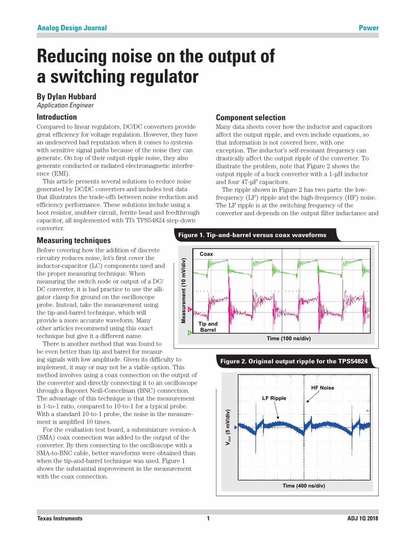
Measuring techniquesBefore covering how the addition of discrete circuitry reduces noise, let’s first cover the inductor-capacitor (LC) components used and the proper measuring technique. When measuring the switch node or output of a DC/DC converter, it is bad practice to use the alli-gator clamp for ground on the oscilloscope probe. Instead, take the measurement using the tip-and-barrel technique, which will provide a more accurate waveform. Many other articles recommend using this exact technique but give it a different name.
There is another method that was found to be even better than tip and barrel for measur-ing signals with low amplitude. Given its difficulty to implement, it may or may not be a viable option. This method involves using a coax connection on the output of the converter and directly connecting it to an oscilloscope through a Bayonet Neill-Concelman (BNC) connection. The advantage of this technique is that the measurement is 1-to-1 ratio, compared to 10-to-1 for a typical probe. With a standard 10-to-1 probe, the noise in the measure-ment is amplified 10 times.
For the evaluation test board, a subminiature version-A (SMA) coax connection was added to the output of the converter. By then connecting to the oscilloscope with a SMA-to-BNC cable, better waveforms were obtained than when the tip-and-barrel technique was used. Figure 1 shows the substantial improvement in the measurement with the coax connection.
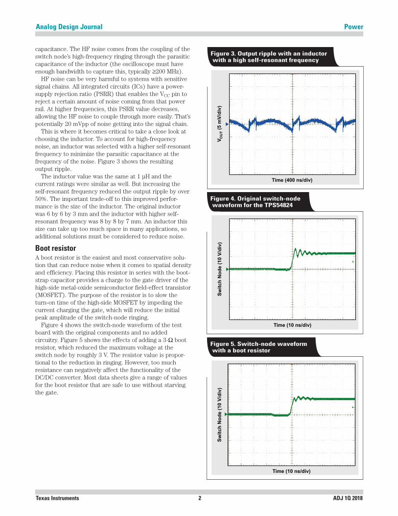
Component selectionMany data sheets cover how the inductor and capacitors affect the output ripple, and even include equations, so that information is not covered here, with one exception. The inductor’s self-resonant frequency can drastically affect the output ripple of the converter. To illustrate the problem, note that Figure 2 shows the output ripple of a buck converter with a 1-µH inductor and four 47-µF capacitors.
The ripple shown in Figure 2 has two parts: the low-frequency (LF) ripple and the high-frequency (HF) noise. The LF ripple is at the switching frequency of the converter and depends on the output filter inductance and
By Dylan HubbardApplication Engineer
Figure 1. Tip-and-barrel versus coax waveforms
Measu
rem
en
t (1
0 m
V/d
iv)
Time (100 ns/div)4
2
Tip andBarrel
Coax
Figure 2. Original output ripple for the TPS54824
LF Ripple
V(5
mV
/div
)O
UT
HF Noise
Time (400 ns/div)
Texas Instruments 2 ADJ 1Q 2018
PowerAnalog Design Journal
capacitance. The HF noise comes from the coupling of the switch node’s high-frequency ringing through the parasitic capacitance of the inductor (the oscilloscope must have enough bandwidth to capture this, typically ≥200 MHz).
HF noise can be very harmful to systems with sensitive signal chains. All integrated circuits (ICs) have a power-supply rejection ratio (PSRR) that enables the VCC pin to reject a certain amount of noise coming from that power rail. At higher frequencies, this PSRR value decreases, allowing the HF noise to couple through more easily. That’s potentially 20 mVpp of noise getting into the signal chain.
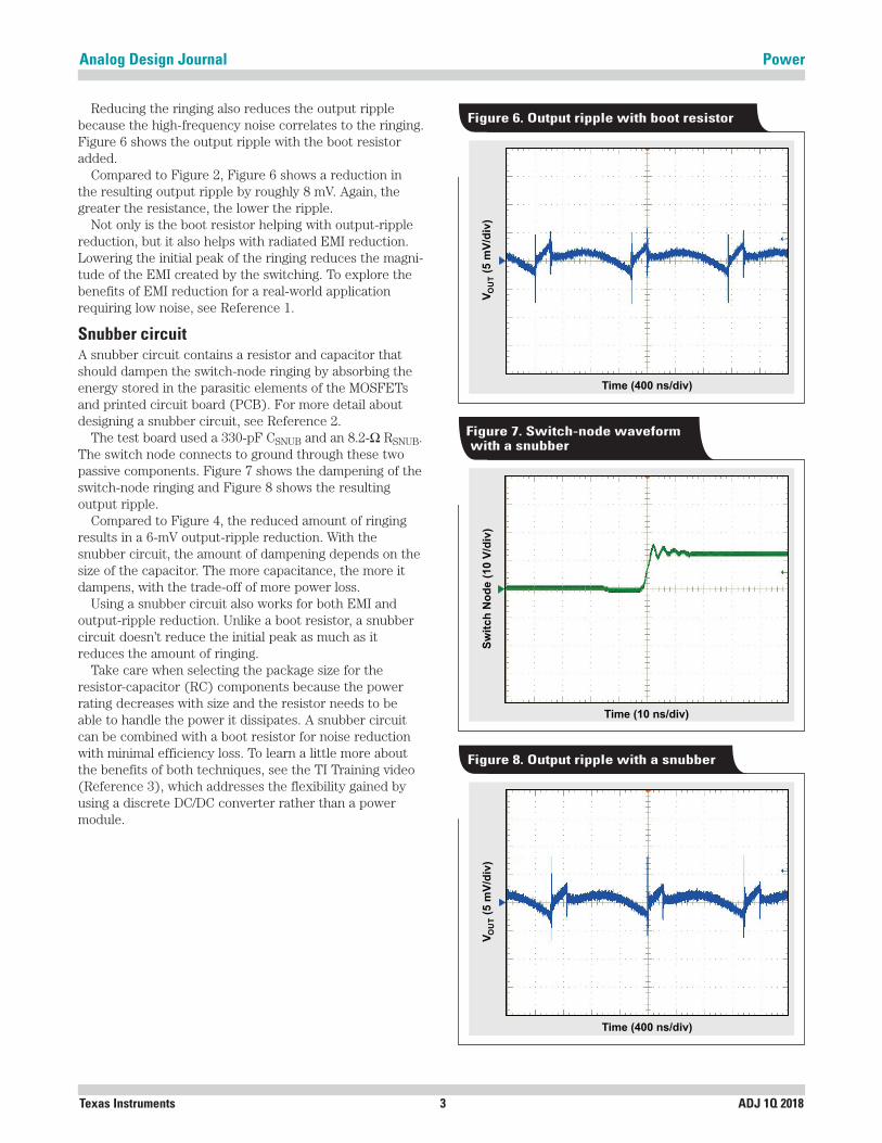
This is where it becomes critical to take a close look at choosing the inductor. To account for high-frequency noise, an inductor was selected with a higher self-resonant frequency to minimize the parasitic capacitance at the frequency of the noise. Figure 3 shows the resulting output ripple.
The inductor value was the same at 1 µH and the current ratings were similar as well. But increasing the self-resonant frequency reduced the output ripple by over 50%. The important trade-off to this improved perfor-mance is the size of the inductor. The original inductor was 6 by 6 by 3 mm and the inductor with higher self-resonant frequency was 8 by 8 by 7 mm. An inductor this size can take up too much space in many applications, so additional solutions must be considered to reduce noise.
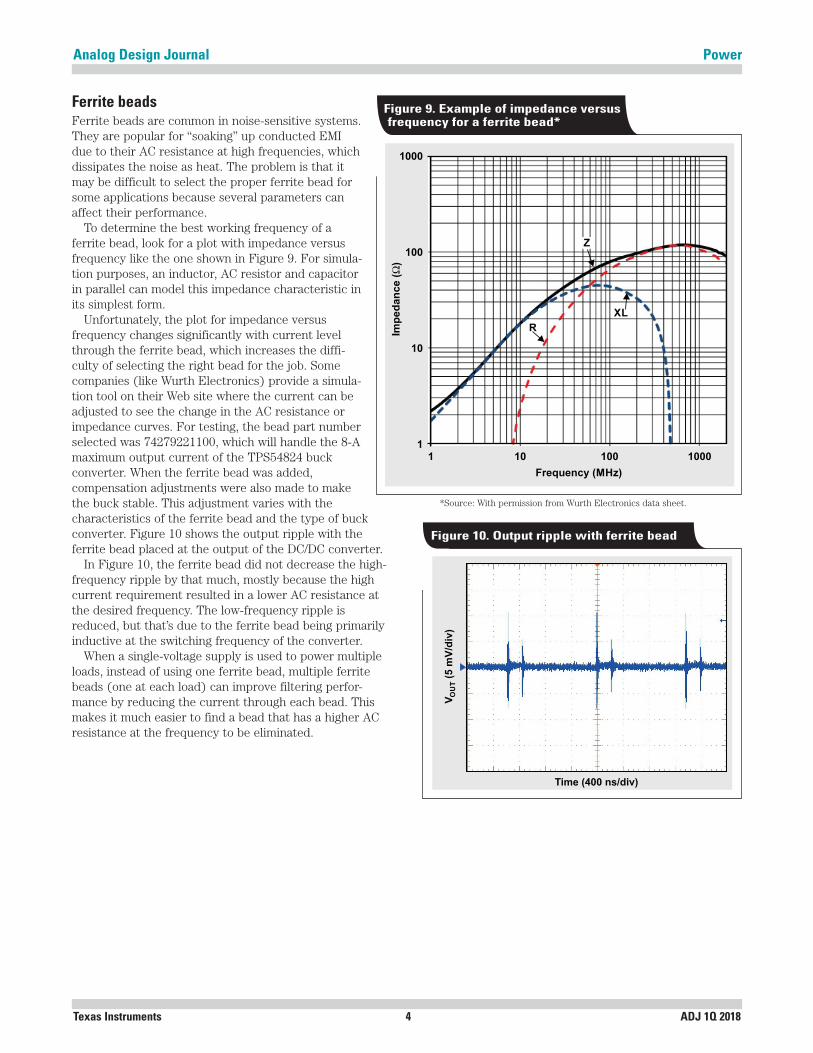
Boot resistorA boot resistor is the easiest and most conservative solu-tion that can reduce noise when it comes to spatial density and efficiency. Placing this resistor in series with the boot-strap capacitor provides a charge to the gate driver of the high-side metal-oxide semiconductor field-effect transistor (MOSFET). The purpose of the resistor is to slow the turn-on time of the high-side MOSFET by impeding the current charging the gate, which will reduce the initial peak amplitude of the switch-node ringing.
Figure 4 shows the switch-node waveform of the test board with the original components and no added circuitry. Figure 5 shows the effects of adding a 3-Ω boot resistor, which reduced the maximum voltage at the switch node by roughly 3 V. The resistor value is propor-tional to the reduction in ringing. However, too much resistance can negatively affect the functionality of the DC/DC converter. Most data sheets give a range of values for the boot resistor that are safe to use without starving the gate.
Figure 3. Output ripple with an inductor with a high self-resonant frequency
V(5
mV
/div
)O
UT
Time (400 ns/div)
Figure 4. Original switch-node waveform for the TPS54824
Sw
itc
h N
od
e (
10
V/d
iv)
Time (10 ns/div)
Figure 5. Switch-node waveform with a boot resistor
Sw
itc
h N
od
e (
10
V/d
iv)
Time (10 ns/div)
Texas Instruments 3 ADJ 1Q 2018
PowerAnalog Design Journal
Reducing the ringing also reduces the output ripple because the high-frequency noise correlates to the ringing. Figure 6 shows the output ripple with the boot resistor added.
Compared to Figure 2, Figure 6 shows a reduction in the resulting output ripple by roughly 8 mV. Again, the greater the resistance, the lower the ripple.
Not only is the boot resistor helping with output-ripple reduction, but it also helps with radiated EMI reduction. Lowering the initial peak of the ringing reduces the magni-tude of the EMI created by the switching. To explore the benefits of EMI reduction for a real-world application requiring low noise, see Reference 1.
Snubber circuitA snubber circuit contains a resistor and capacitor that should dampen the switch-node ringing by absorbing the energy stored in the parasitic elements of the MOSFETs and printed circuit board (PCB). For more detail about designing a snubber circuit, see Reference 2.
The test board used a 330-pF CSNUB and an 8.2-Ω RSNUB. The switch node connects to ground through these two passive components. Figure 7 shows the dampening of the switch-node ringing and Figure 8 shows the resulting output ripple.
Compared to Figure 4, the reduced amount of ringing results in a 6-mV output-ripple reduction. With the snubber circuit, the amount of dampening depends on the size of the capacitor. The more capacitance, the more it dampens, with the trade-off of more power loss.
Using a snubber circuit also works for both EMI and output-ripple reduction. Unlike a boot resistor, a snubber circuit doesn’t reduce the initial peak as much as it reduces the amount of ringing.
Take care when selecting the package size for the resistor-capacitor (RC) components because the power rating decreases with size and the resistor needs to be able to handle the power it dissipates. A snubber circuit can be combined with a boot resistor for noise reduction with minimal efficiency loss. To learn a little more about the benefits of both techniques, see the TI Training video (Reference 3), which addresses the flexibility gained by using a discrete DC/DC converter rather than a power module.
Figure 6. Output ripple with boot resistor
Time (400 ns/div)
V(5
mV
/div
)O
UT
Figure 7. Switch-node waveform with a snubber
Sw
itch
No
de (
10 V
/div
)
Time (10 ns/div)
Figure 8. Output ripple with a snubber
Time (400 ns/div)
V(5
mV
/div
)O
UT
Texas Instruments 4 ADJ 1Q 2018
PowerAnalog Design Journal
Ferrite beadsFerrite beads are common in noise-sensitive systems. They are popular for “soaking” up conducted EMI due to their AC resistance at high frequencies, which dissipates the noise as heat. The problem is that it may be difficult to select the proper ferrite bead for some applications because several parameters can affect their performance.
To determine the best working frequency of a ferrite bead, look for a plot with impedance versus frequency like the one shown in Figure 9. For simula-tion purposes, an inductor, AC resistor and capacitor in parallel can model this impedance characteristic in its simplest form.
Unfortunately, the plot for impedance versus frequency changes significantly with current level through the ferrite bead, which increases the diffi-culty of selecting the right bead for the job. Some companies (like Wurth Electronics) provide a simula-tion tool on their Web site where the current can be adjusted to see the change in the AC resistance or impedance curves. For testing, the bead part number selected was 74279221100, which will handle the 8-A maximum output current of the TPS54824 buck converter. When the ferrite bead was added, compensation adjustments were also made to make the buck stable. This adjustment varies with the characteristics of the ferrite bead and the type of buck converter. Figure 10 shows the output ripple with the ferrite bead placed at the output of the DC/DC converter.
In Figure 10, the ferrite bead did not decrease the high-frequency ripple by that much, mostly because the high current requirement resulted in a lower AC resistance at the desired frequency. The low-frequency ripple is reduced, but that’s due to the ferrite bead being primarily inductive at the switching frequency of the converter.
When a single-voltage supply is used to power multiple loads, instead of using one ferrite bead, multiple ferrite beads (one at each load) can improve filtering perfor-mance by reducing the current through each bead. This makes it much easier to find a bead that has a higher AC resistance at the frequency to be eliminated.
Figure 9. Example of impedance versus frequency for a ferrite bead*
1 10 100 1000
Frequency (MHz)
Imp
ed
an
ce (
)Ω
1000
100
10
1
Z
RR
XL
*Source: With permission from Wurth Electronics data sheet.
Figure 10. Output ripple with ferrite bead
Time (400 ns/div)
V(5
mV
/div
)O
UT
Texas Instruments 5 ADJ 1Q 2018
PowerAnalog Design Journal
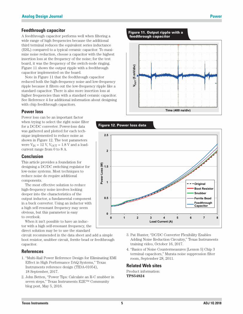
Feedthrough capacitorA feedthrough capacitor performs well when filtering a wide range of high frequencies because the additional third terminal reduces the equivalent series inductance (ESL) compared to a typical ceramic capacitor. To maxi-mize noise reduction, choose a capacitor with the highest insertion loss at the frequency of the noise; for the test board, it was the frequency of the switch-node ringing. Figure 11 shows the output ripple with a feedthrough capacitor implemented on the board.
Note in Figure 11 that the feedthrough capacitor reduced both the high-frequency noise and low-frequency ripple because it filters out the low-frequency ripple like a standard capacitor. There is also more insertion loss at higher frequencies than with a standard ceramic capacitor. See Reference 4 for additional information about designing with chip feedthrough capacitors.
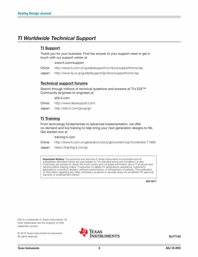
Power lossPower loss can be an important factor when trying to select the right noise filter for a DC/DC converter. Power-loss data was gathered and plotted for each tech-nique implemented to reduce noise as shown in Figure 12. The test parameters were VIN = 12 V, VOUT = 1.8 V and a load-current range from 0 to 8 A.
ConclusionThis article provides a foundation for designing a DC/DC switching regulator for low-noise systems. Most techniques to reduce noise do require additional components.
The most effective solution to reduce high-frequency noise involves looking deeper into the characteristics of the output inductor, a fundamental component in a buck converter. Using an inductor with a high self-resonant frequency may seem obvious, but this parameter is easy to overlook.
When it isn’t possible to have an induc-tor with a high self-resonant frequency, the direct solution may be to use the standard circuit recommended in the data sheet and add a simple boot resistor, snubber circuit, ferrite bead or feedthrough capacitor.
References1. “Multi-Rail Power Reference Design for Eliminating EMI
Effect in High Performance DAQ Systems,” Texas Instruments reference design (TIDA-01054), 18 September, 2017.
2. John Betten, “Power Tips: Calculate an R-C snubber in seven steps,” Texas Instruments E2E™ Community blog post, May 5, 2016.
Figure 11. Output ripple with a feedthrough capacitor
Time (400 ns/div)
V(5
mV
/div
)O
UT
Figure 12. Power loss data
0
0.5
1
1.5
2
2.5
0 1 2 3 4 5 6 7 8
Po
we
r L
os
s (
W)
Load Current (A)
Original
Boot Resistor
Snubber
Ferrite Bead
FeedthroughCapacitor
3. Pat Hunter, “DC/DC Converter Flexibility Enables Adding Noise Reduction Circuitry,” Texas Instruments training video, October 16, 2017.
4. “Basics of Noise Countermeasures [Lesson 5] Chip 3 terminal capacitors,” Murata noise suppression filter room, September 28, 2011.
Related Web sitesProduct information:TPS54824
Texas Instruments 6 ADJ 1Q 2018
Analog Design Journal
E2E is a trademark of Texas Instruments. All other trademarks are the property of their respective owners.
TI Worldwide Technical Support
TI SupportThank you for your business. Find the answer to your support need or get in touch with our support center at
www.ti.com/support
China: http://www.ti.com.cn/guidedsupport/cn/docs/supporthome.tsp
Japan: http://www.tij.co.jp/guidedsupport/jp/docs/supporthome.tsp
Technical support forumsSearch through millions of technical questions and answers at TI’s E2E™ Community (engineer-to-engineer) at
e2e.ti.com
China: http://www.deyisupport.com/
Japan: http://e2e.ti.com/group/jp/
TI TrainingFrom technology fundamentals to advanced implementation, we offer on-demand and live training to help bring your next-generation designs to life. Get started now at
training.ti.com
China: http://www.ti.com.cn/general/cn/docs/gencontent.tsp?contentId=71968
Japan: https://training.ti.com/jp
A011617
Important Notice: The products and services of Texas Instruments Incorporated and its subsidiaries described herein are sold subject to TI’s standard terms and conditions of sale. Customers are advised to obtain the most current and complete information about TI products and services before placing orders. TI assumes no liability for applications assistance, customer’s applications or product designs, software performance, or infringement of patents. The publication of information regarding any other company’s products or services does not constitute TI’s approval, warranty or endorsement thereof.
© 2018 Texas Instruments Incorporated. All rights reserved. SLYT740

IMPORTANT NOTICE FOR TI DESIGN INFORMATION AND RESOURCES
Texas Instruments Incorporated (‘TI”) technical, application or other design advice, services or information, including, but not limited to,reference designs and materials relating to evaluation modules, (collectively, “TI Resources”) are intended to assist designers who aredeveloping applications that incorporate TI products; by downloading, accessing or using any particular TI Resource in any way, you(individually or, if you are acting on behalf of a company, your company) agree to use it solely for this purpose and subject to the terms ofthis Notice.TI’s provision of TI Resources does not expand or otherwise alter TI’s applicable published warranties or warranty disclaimers for TIproducts, and no additional obligations or liabilities arise from TI providing such TI Resources. TI reserves the right to make corrections,enhancements, improvements and other changes to its TI Resources.You understand and agree that you remain responsible for using your independent analysis, evaluation and judgment in designing yourapplications and that you have full and exclusive responsibility to assure the safety of your applications and compliance of your applications(and of all TI products used in or for your applications) with all applicable regulations, laws and other applicable requirements. Yourepresent that, with respect to your applications, you have all the necessary expertise to create and implement safeguards that (1)anticipate dangerous consequences of failures, (2) monitor failures and their consequences, and (3) lessen the likelihood of failures thatmight cause harm and take appropriate actions. You agree that prior to using or distributing any applications that include TI products, youwill thoroughly test such applications and the functionality of such TI products as used in such applications. TI has not conducted anytesting other than that specifically described in the published documentation for a particular TI Resource.You are authorized to use, copy and modify any individual TI Resource only in connection with the development of applications that includethe TI product(s) identified in such TI Resource. NO OTHER LICENSE, EXPRESS OR IMPLIED, BY ESTOPPEL OR OTHERWISE TOANY OTHER TI INTELLECTUAL PROPERTY RIGHT, AND NO LICENSE TO ANY TECHNOLOGY OR INTELLECTUAL PROPERTYRIGHT OF TI OR ANY THIRD PARTY IS GRANTED HEREIN, including but not limited to any patent right, copyright, mask work right, orother intellectual property right relating to any combination, machine, or process in which TI products or services are used. Informationregarding or referencing third-party products or services does not constitute a license to use such products or services, or a warranty orendorsement thereof. Use of TI Resources may require a license from a third party under the patents or other intellectual property of thethird party, or a license from TI under the patents or other intellectual property of TI.TI RESOURCES ARE PROVIDED “AS IS” AND WITH ALL FAULTS. TI DISCLAIMS ALL OTHER WARRANTIES ORREPRESENTATIONS, EXPRESS OR IMPLIED, REGARDING TI RESOURCES OR USE THEREOF, INCLUDING BUT NOT LIMITED TOACCURACY OR COMPLETENESS, TITLE, ANY EPIDEMIC FAILURE WARRANTY AND ANY IMPLIED WARRANTIES OFMERCHANTABILITY, FITNESS FOR A PARTICULAR PURPOSE, AND NON-INFRINGEMENT OF ANY THIRD PARTY INTELLECTUALPROPERTY RIGHTS.TI SHALL NOT BE LIABLE FOR AND SHALL NOT DEFEND OR INDEMNIFY YOU AGAINST ANY CLAIM, INCLUDING BUT NOTLIMITED TO ANY INFRINGEMENT CLAIM THAT RELATES TO OR IS BASED ON ANY COMBINATION OF PRODUCTS EVEN IFDESCRIBED IN TI RESOURCES OR OTHERWISE. IN NO EVENT SHALL TI BE LIABLE FOR ANY ACTUAL, DIRECT, SPECIAL,COLLATERAL, INDIRECT, PUNITIVE, INCIDENTAL, CONSEQUENTIAL OR EXEMPLARY DAMAGES IN CONNECTION WITH ORARISING OUT OF TI RESOURCES OR USE THEREOF, AND REGARDLESS OF WHETHER TI HAS BEEN ADVISED OF THEPOSSIBILITY OF SUCH DAMAGES.You agree to fully indemnify TI and its representatives against any damages, costs, losses, and/or liabilities arising out of your non-compliance with the terms and provisions of this Notice.This Notice applies to TI Resources. Additional terms apply to the use and purchase of certain types of materials, TI products and services.These include; without limitation, TI’s standard terms for semiconductor products http://www.ti.com/sc/docs/stdterms.htm), evaluationmodules, and samples (http://www.ti.com/sc/docs/sampterms.htm).
Mailing Address: Texas Instruments, Post Office Box 655303, Dallas, Texas 75265Copyright © 2018, Texas Instruments Incorporated