reduction of emi due to common mode current using common
TRANSCRIPT

Scholars' Mine Scholars' Mine
Masters Theses Student Theses and Dissertations
Fall 2016
Reduction of EMI due to common mode current using common Reduction of EMI due to common mode current using common
mode filter or lossy material mode filter or lossy material
Qian Liu
Follow this and additional works at: https://scholarsmine.mst.edu/masters_theses
Part of the Electrical and Computer Engineering Commons
Department: Department:
Recommended Citation Recommended Citation Liu, Qian, "Reduction of EMI due to common mode current using common mode filter or lossy material" (2016). Masters Theses. 7622. https://scholarsmine.mst.edu/masters_theses/7622
This thesis is brought to you by Scholars' Mine, a service of the Missouri S&T Library and Learning Resources. This work is protected by U. S. Copyright Law. Unauthorized use including reproduction for redistribution requires the permission of the copyright holder. For more information, please contact [email protected].
ii
REDUCTION OF EMI DUE TO COMMON MODE CURRENT USING COMMON
MODE FILTER OR LOSSY MATERIAL
by
QIAN LIU
A THESIS
Presented to the Faculty of the Graduate School of the
MISSOURI UNIVERSITY OF SCIENCE AND TECHNOLOGY
In Partial Fulfillment of the Requirements for the Degree
MASTER OF SCIENCE IN ELECTRICAL ENGINEERING
2016
Approved by
Victor Khilkevich, Advisor
David J. Pommerenke
Jun Fan

iii
2016
Qian Liu
All Rights Reserved

iii
PUBLICATION THESIS OPTION
This thesis consists of the following four papers, formatted in the style used by
the Missouri University of Science and Technology, listed as follows:
Page 2-25 are intended for submission to the IEEE TRANSATIONS ON
ELECTROMAGNETIC COMPATIBILITY.
Page 26-42 are intended for submission to the IEEE LETTER ON
ELECTROMAGNETIC COMPATIBILITY.
Page 43-60 are intended for submission to the IEEE INTERNATIONAL
CONFERENCE ON ELECTROMAGNETIC COMPATIBILITY.
Page 61-75 are intended for submission to the IEEE INTERNATIONAL
CONFERENCE ON ELECTROMAGNETIC COMPATIBILITY.
iv
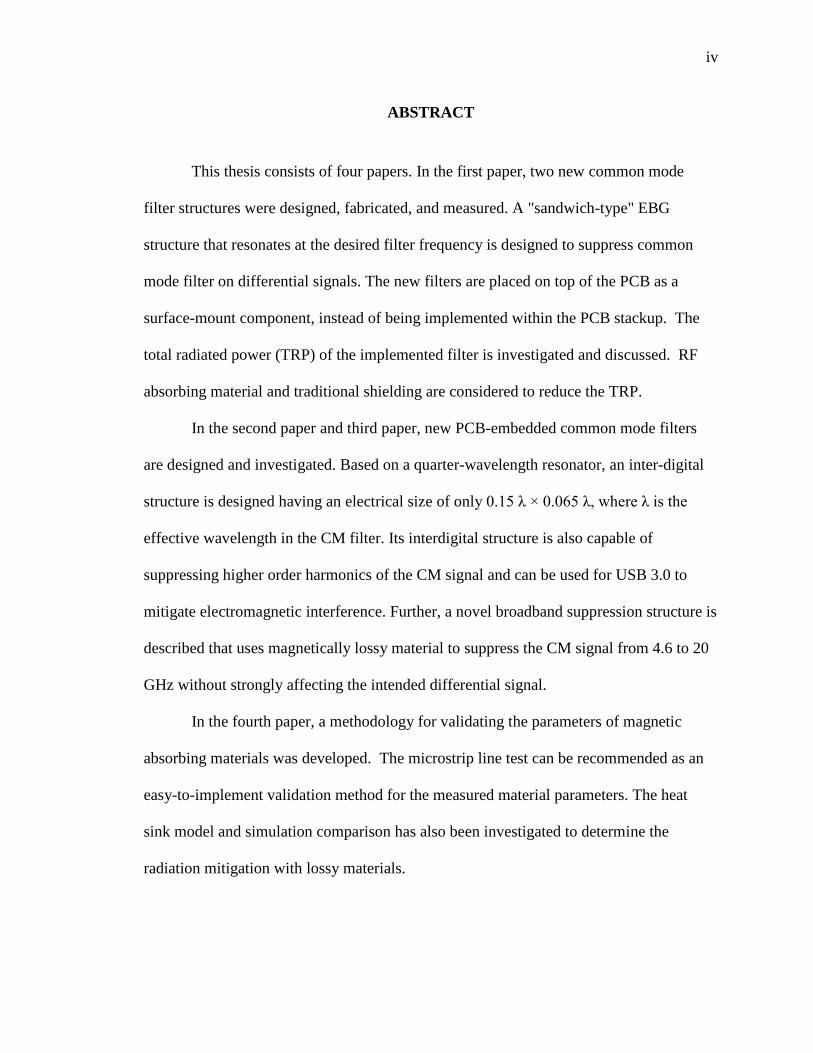
ABSTRACT
This thesis consists of four papers. In the first paper, two new common mode
filter structures were designed, fabricated, and measured. A "sandwich-type" EBG
structure that resonates at the desired filter frequency is designed to suppress common
mode filter on differential signals. The new filters are placed on top of the PCB as a
surface-mount component, instead of being implemented within the PCB stackup. The
total radiated power (TRP) of the implemented filter is investigated and discussed. RF
absorbing material and traditional shielding are considered to reduce the TRP.
In the second paper and third paper, new PCB-embedded common mode filters
are designed and investigated. Based on a quarter-wavelength resonator, an inter-digital
structure is designed having an electrical size of only 0.15 λ × 0.065 λ, where λ is the
effective wavelength in the CM filter. Its interdigital structure is also capable of
suppressing higher order harmonics of the CM signal and can be used for USB 3.0 to
mitigate electromagnetic interference. Further, a novel broadband suppression structure is
described that uses magnetically lossy material to suppress the CM signal from 4.6 to 20
GHz without strongly affecting the intended differential signal.
In the fourth paper, a methodology for validating the parameters of magnetic
absorbing materials was developed. The microstrip line test can be recommended as an
easy-to-implement validation method for the measured material parameters. The heat
sink model and simulation comparison has also been investigated to determine the
radiation mitigation with lossy materials.
v
ACKNOWLEDGMENTS
I would like to express my sincere gratitude to Dr. Victor Khilkevich, my advisor,
for his guidance and instruction on my research work, financial support to my study and
direction for this thesis during my pursuit of the Master’s degree. I learned not only
academic knowledge from Dr. Khilkevich, but also the rigorous attitude, good manners,
and courage to face difficulties.
I would like to thank Dr. Jun Fan, Dr. David Pommerenke and Dr. James
Drewniak for their teaching in my courses, discussions related to my research and helpful
suggestions on my thesis.
I would also like to express my thanks to all the other faculty members and
students in and out of the EMC lab for their team work and help in my coursework and
research.
Finally, my heartfelt gratitude goes to my parents and my husband, Sen Yang, for
their support and encouragement towards achieving this goal.
vi
TABLE OF CONTENTS
Page
PUBLICATION THESIS OPTION ................................................................................... iii
ABSTRACT ....................................................................................................................... iv
ACKNOWLEDGMENTS .................................................................................................. v
LIST OF ILLUSTRATIONS ........................................................................................... viii
LIST OF TABLES ............................................................................................................. xi
SECTION
1.INTRODUCTION ....................................................................................................... 1
PAPER
I. REDUCTION OF EMI DUE TO COMMON MODE CURRENTS USING A
SURFACE-MOUBT, EBG-BASED FILTER ............................................................ 2
ABSTRACT ............................................................................................................. 2
1. INTRODUCTION ................................................................................................ 3
2. INSPIRATION AND DESIGN CONCEPT ......................................................... 5
3. SIMULATION AND MEASUREMENT RESULT ANALYSIS ....................... 7
4. ANALYSIS OF TOTAL RADIATED POWER ................................................ 15
5. CONCLUSION .................................................................................................. 22
REFERENCES ............................................................................................................. 23
II.COMMON-MODE FILTERS WITH INTERDIGITAL FINGERS FOR
HARMONICS SUPPRESSION AND LOSSY MATERIALS FOR
BROADBAND SUPPRESSION .............................................................................. 26
ABSTRACT ........................................................................................................... 26
1. INTRODUCTION .............................................................................................. 27
2. NARROWBAND CM SUPRESSION FILTER ................................................ 28
3. BROADBAND CM SUPPRESSION FILTER .................................................. 34
4. COMBINED CM SUPPRESSION FILTER ...................................................... 38
5. CONCLUSION .................................................................................................. 41
REFERENCES ............................................................................................................. 42
III. PCB STRUCTURE FOR COMMON MODE SUPPRESSION ON
DIFFEREITNAIL MICROSTRIP LINES .............................................................. 43
ABSTRACT ........................................................................................................... 43
vii
1. INTRODUCTION .............................................................................................. 44
2. DESIGN CONCEPT .......................................................................................... 46
3. BASIC STRUCTURE: QUART WAVELENGTH FILTER ............................. 48
4. TECHNIQUES FOR REDUCING SIZE ........................................................... 51
4.1. ADDING INTEGRATED CAPACITANCE AT THE END OF THE
EXTRA TRACE. ....................................................................................... 51
4.2. RESONATOR UNDERNEATH THE DIFFERENTIAL TRACE ........... 52
5. PROPOSED NOVEL STRUCTURE ................................................................. 55
6. CONCLUSION .................................................................................................. 58
REFERENCES ............................................................................................................. 59
IV. MODELING ABSORBING MATERIALS FOR EMI MITIGATION ................ 61
ABSTRACT ........................................................................................................... 61
1. INTRODUCTION .............................................................................................. 62
2. MEASUREMENT OF MATERIAL PARAMETERS....................................... 63
3. MODELING MICROSTRIP LINE FOR VALIDATION MATERIAL
PROPERTIES .................................................................................................... 66
4. APPLICATION TO THE HEATSINK .............................................................. 69
5. CONCLUSION .................................................................................................. 73
REFERENCES ............................................................................................................. 74
SECTION
2. CONCLUSIONS ................................................................................................ 76
VITA .................................................................................................................................77
viii
LIST OF ILLUSTRATIONS
Page
PAPER I
Figure 2.1. Top view of the EBG configuration. ............................................................... 5
Figure 2.2. EBG configuration with a "sandwich" structure. ............................................ 6
Figure 3.1. Stackup cross section of removable “sandwich” EBG. ................................... 7
Figure 3.2. Removable “sandwich” EBG configuration (stripline) ................................... 8
Figure 3.3. Top view of removable part: layer one, four and six for stripline, layer
two, four and six for microstrip line. ............................................................... 9
Figure 3.4. Removable “sandwich” EBG configuration (microstrip line)....................... 10
Figure 3.5. Stripline’s simulated and measured S-parameter comparison....................... 11
Figure 3.6. Mcrostrip line’s simulated and measured S-parameter comparison.............. 12
Figure 3.7. Top view of surface-mount EBG patches showing the relative positions
of the connection vias for both the models in Fig.3.2 and Fig.3.4. ............... 13
Figure 3.8. Simulation results coming from the different placements of the
connection vias in both the R-EBG structures. .............................................. 14
Figure 4.1. Spatial distribution of the magnitude of E-Field on the removable EBG
—stripline. ..................................................................................................... 15
Figure 4.2. Spatial distribution of the magnitude of E-Field on the removable
EBG—microstrip line .................................................................................... 16
Figure 4.3. Measured TRP results comparison. ............................................................... 17
Figure 4.4. Picture frame of lossy material on the removable EBG board. ..................... 18
Figure 4.5. Measured TRP results comparison for lossy material ................................... 18
Figure 4.6. S-parameter (before de-embedding) comparison--with 2 layers of
material vs. without lossy material. ............................................................... 19
Figure 4.7. Experiment setup for measuring the total radiated power ............................. 20
Figure 4.8. Measured TRP results comparison between a reference board and a
removable RBG filter. ................................................................................... 21
PAPER II
Figure 2.1. Structure of a CM filter based on a quarter-wavelength resonator. .............. 28
Figure 2.2. Proposed CM suppression filter .................................................................... 29
Figure 2.3. Simulated and measured differential insertion loss |Sdd| and |Scc| for the
proposed CM suppression filter with interdigital stubs. ................................ 30
ix
Figure 2.4. Top view of the structure on layer 2 .............................................................. 30
Figure 2.5. Comparison of the simulated results of the structures in Figure 2.4. ............ 31
Figure 2.6. Effect of interdigital stub length L1 on the center frequency of the CM
suppression filter. ........................................................................................... 31
Figure 2.7. Simulated differential insertion loss |Sdd | and |Scc | for the proposed
CM suppression filter operating at 6 GHz. .................................................... 32
Figure 3.1. Conceptual field distribution ......................................................................... 34
Figure 3.2. Simulated H-field distribution around a differential trace ............................ 35
Figure 3.3. Proposed broadband CM suppression filter .................................................. 36
Figure 3.4. Effect on insertion loss |Scc21 | and |Sdd21 | as a function of the distance
between the added conductor and the differential trace. ............................... 36
Figure 3.5. Simulated eye diagrams of a differential trace .............................................. 37
Figure 4.1. Geometry of a resonator as a basis for overlaying lossy material for a
broadband CM suppression filter ................................................................... 39
Figure 4.2. Simulated and measured data comparison for the structure in Figure 4.1. ... 39
Figure 4.3. Simulated and measured data comparison of combined structures. .............. 40
PAPER III
Figure 2.1. (a) E-field and H-field for DM in differential pairs (b) E-field and H-
field for CM in differential pairs (c) E-field and H-field for DM in
differential pairs after adding a thin metal plane (d) E-field and H-field
for CM in differential pairs after adding a thin metal plane .......................... 46
Figure 3.1. (a) Configuration of common-mode filter in 3-D view (b) Configuration
of common-mode filter in cross-section view 1 (c) Configuration of
common-mode filter in cross-section view 2. ................................................ 49
Figure 3.2. Comparisons of the simulation results of S-parameters between full-
wave simulation and test PCB board measurement for Figure 3.1................ 50
Figure 4.1. Configuration of common-mode filter after adding capacitors at the end
of quarter-wavelength resonators in 3-D view. ............................................. 51
Figure 4.2. Comparison of measured response for normal quarter wavelength
resonator structure to the same structure with added 1 pF capacitors. .......... 52
Figure 4.3. (a) Configuration of the common-mode filter in 3-D view (b)
Configuration of the common-mode filter in cross-sectional view. .............. 53
Figure 4.4. Full wave simulated S-parameters for the structure shown in Figure 4.3. .... 54
Figure 4.5. (a) Inductive loaded for resonator and (b) Cross-section for added traces
underneath ground plane for reduced resonance frequency. ......................... 54
Figure 5.1. (a) Configuration of the new CMF in 3-D view (b) Cross-sectional view
(c) Top view for the second layer and (d) Top view of second layer ............ 55
x
Figure 5.2. Simulation results of the S-parameters from full-wave simulation for the
structure shown in Figure 5.1 ........................................................................ 57
PAPER IV
Figure 2.1. The permittivity (a) and permibility (b) of Material A.................................. 64
Figure 2.2. The permittivity (a) and permeability (b) of material B. ............................... 65
Figure 3.1. Variation of emissions from cables under CM and DM excitations. ............ 66
Figure 3.2. The comparison between simulation and measurement for the microstrip
line. ................................................................................................................ 67
Figure 3.3. S-parameters measurement setup for determining lossy material
properties. ...................................................................................................... 67
Figure 3.4. CST Microwave Studio model of mocristrip line with lossy material. ......... 68
Figure 3.5. The comparison between simulation and measurement for the microstrip
line with lossy material. ................................................................................. 68
Figure 4.1. Side view of measured heatsink with square metal patch as the
excitation. ....................................................................................................... 70
Figure 4.2. CST Microwave Studio model ...................................................................... 70
Figure 4.3. Setup for chamber calibration. ...................................................................... 71
Figure 4.4. Setup for total radiation measurement. .......................................................... 71
Figure 4.5. Comparison of simulated and measured results of radiation power. ............. 72
Figure 4.6. Comparison of simulated and measured results of total radiation
reduction (shielding effectiveness). ............................................................... 72
xi
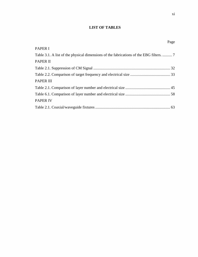
LIST OF TABLES
Page
PAPER I
Table 3.1. A list of the physical dimensions of the fabrications of the EBG filters. .......... 7
PAPER II
Table 2.1. Suppression of CM Signal ............................................................................... 32
Table 2.2. Comparison of target frequency and electrical size ......................................... 33
PAPER III
Table 2.1. Comparison of layer number and electrical size .............................................. 45
Table 6.1. Comparison of layer number and electrical size .............................................. 58
PAPER IV
Table 2.1. Coaxial/waveguide fixtures ............................................................................. 63
1
1. INTRODUCTION
In the real world, small asymmetries in the differential pair can have a large
impact on electromagnetic compatibility (EMC) and signal integrity (SI) if not handled
properly. The discontinues will dramatically increase the amount of common mode (CM)
noise seen at the receiver, increases the emissions from the CM current and thus
interference and crosstalk problems. Paper I, Paper II and Paper III will discuss different
kind of common mode filter. The filter can be used in the printed circuit board and
suppress the common at the desireable frequency, which can decrease EMI.
Absorbing materials for reduction of electromagnetic interference (EMI) are
typically used at later stages of electronic product development as a practical
countermeasure to possible regulatory issues. Design consideration for absorbing
materials at earlier stages could be beneficial to provide cost-effective solutions. Paper IV
gives a method to get the material parameters and vidation. Knowing the permeability (μ)
and permittivity (ε) of the lossy material to be able to choose the appropriate material
from a number of available candidates and predict the performance of the EMI mitigation
solution. Finally, measurement and simulation are done to investigate the sheilding
effectiness of the lossy material.
2
PAPER
I. REDUCTION OF EMI DUE TO COMMON MODE CURRENTS USING A
SURFACE-MOUBT, EBG-BASED FILTER
Qian Liu, Student Member, IEEE, Sam Connor, Senior Member, IEEE, Carlo
Olivieri, Member, IEEE, Francesco de Paulis, Member, IEEE, Antonio Orlandi, Fellow,
IEEE, Michael Cracraft, Member, IEEE, Bruce Archambeault, Fellow, IEEE, Victor
Khilkevich, Member, IEEE
ABSTRACT
Common mode (CM) noise on differential signals can be suppressed by planar
Electromagnetic Band-gap (EBG) technologies. In this work, two new common mode
filter structures were designed, fabricated, and measured. The filters are based on a
previously proposed geometry, a "sandwich-type" EBG structure that resonates at the
desired filter frequency; however, the new filters are placed on top of the PCB as a
surface-mount component, instead of being implemented within the PCB stackup.
Stripline and microstrip versions of the removable filter are considered. The filters can be
easily removed and substituted with another one that is designed to filter a different
frequency but maintains the same footprint and external dimensions. In addition, the
surface-mount filter allows us to incorporate DC blocking capacitors into the microstrip
version of the filter, thus providing two functions in one package. The total radiated
power (TRP) of the implemented filter is investigated and discussed. RF absorbing
material and traditional shielding are considered to reduce the TRP.
Index Terms— Electromagnetic band-gap structures (EBG), common mode filter,
common mode (CM), differential pair, narrowband filter.
3
1. INTRODUCTION
Common mode (CM) noise often induces electromagnetic interference (EMI)
problems. It is caused by imbalances in the differential signal and/or its path [1]. The
increasing bit rate of modern high speed digital electronics leads to increased EMI
problems, such as unwanted radiation to the surrounding environment and coupling to
nearby active and passive devices [2]. Common mode current is recognized as a major
source of radiation and can ultimately deteriorate the signal quality, therefore differential
interconnects have to be designed carefully to minimize any source of imbalance (i.e.
amplitude mismatch, rise/fall time difference). From an EMI point of view, any CM
current flowing on differential interconnects will radiate to some extent. Radiation from
differential wiring on printed circuit boards (PCB) can be mitigated by burying the
signals on internal layers or by placing the PCB within a shielded enclosure, but when the
signals exit the PCB on an I/O cable, the cable may become radiating structure. The
cables can be shielded as well, and often are, but the connection between chassis and
cable shield presents an opportunity for leakage. The best way to mitigate the emissions
from a cable assembly is to attenuate the CM currents significantly before the signals exit
the PCB and enter the cable [3].
Common mode filters are widely used to attenuate common mode noise, while
ensuring the intentional differential signal is unaffected [4]-[7]. The basic filter principle
relies on coupling the common mode energy on the differential traces into resonant
cavities while ensuring the unperturbed propagation of the intentional differential signal.
These common mode filters can be built on a PCB with typical planar technologies [8]-
[12]. Recent studies have focused on the filters that are easy to design and to fabricate.
The filter needs to be compact to be attractive to designers of high density PCBs. These
practical constraints led us to replace the simple planar patch cavity with an EBG
sandwich-type resonant structure [13]-[19].
A further advancement is proposed in this paper: the differential pair transitions
up onto a surface-mount component. This minimizes the impact on the PCB design,
because the solid reference planes are not being etched into periodic patterns, thereby
preventing noise coupling from one cavity into another and also eliminating any concerns
4
with power distribution due to increased IR drop. The idea is to create a standalone filter
that can be easily installed to and removed from the PCB through pads on the PCB’s
outer layers. Given a certain footprint on the PCB, a different resonant frequency can be
obtained by choosing the permittivity of the dielectric and the EBG’s geometric
parameters appropriately. The main drawback with this approach is the variability in
separation distance due to soldering processes, but this drawback is minimized by
keeping the signals and EBG patches off of the bottom layer of the removable part.
Another novel advancement in this paper is that DC blocking capacitors can be placed on
the removable component if the filter is designed with microstrip lines on the top surface.
In this embodiment, two functions are performed by one standalone component.
A detailed investigation of the electromagnetic behavior of this filter structure is
shown below. This work extends the previous studies in [17]-[20], considering the total
radiation issue. Measurement and simulation results are compared to validate the
performance of the removable EBG filter and its design process. Total radiated power is
measured and compared to determine the effectiveness of the standalone filter. In
addition, both RF absorbing material and traditional shielding are explored as methods of
mitigating the added radiation from the removable filter.
5
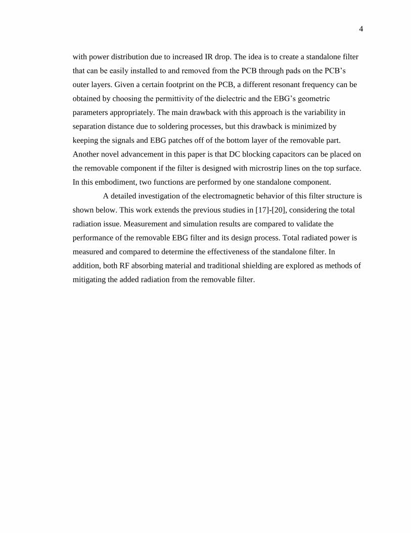
2. INSPIRATION AND DESIGN CONCEPT
The original proposed EBG structure is shown in Figure 2.1 (a) [17]. The
common mode energy will couple into the cavity when the return current reaches the
gaps between adjacent EBGs, reducing the amount of common mode that reaches the
receiver. However, the currents associated with the differential signal pass over the filter
unaffected.
(a) (b)
Figure 2.1. Top view of the EBG configuration: (a) “original” configuration, (b) with
meandered bridges between the patches.
The central patch in the three patches of the original configuration was found to
be unimportant for the construction of a resonant cavity. In order to reduce the required
EBG space, the central patch is replaced by a serpentine trace (called a meandered bridge
in previous papers) which links the remaining two patches, as shown in Figure 2.1(b). A
further size reduction is achieved by folding this structure into a "sandwich-type"
configuration. Figure 2.2 shows the top view and stackup of the EBG "sandwich"
geometry. By introducing two more layers, one row of patches stays on the layer directly
below the traces, but the other row of patches is placed on another layer with a solid
reference layer in between (Figure 2.2 (b)). The patches on different layers are connected
with each other by vias, and antipads are used to isolate the vias from the intermediate
reference plane.

6
(a) (b)
Figure 2.2. EBG configuration with a "sandwich" structure: (a) top view, (b) related
stack-up.
The miniaturized “sandwich-type” EBG described briefly above and more
thoroughly in [17] is combined with the idea of a removable, surface-mount filter [20].
This combination provides good design flexibility, limited costs, and a compact
component. The sandwich structure proposed in [17] could be considered unattractive
since it employs four PCB layers instead of two as in the original planar configuration,
but the combination of the sandwich EBG together with the removable part concept
makes this filter viable. The cost increase due to the more complex component stack-up
and the possible use of expensive laminate material is limited to the small filter footprint
instead of to the PCB as a whole. One limitation during the design process is that the
EBG design procedure presented in [21]-[22] cannot be directly applied to the sandwich
type of layout. The analytical method is only applied to calculate a preliminary patch and
via sizing; then a refinement process must be performed to achieve the target frequency.
The vias are kept as close as possible to the patch in order to minimize the filter area.
Therefore, the tuning involves adjusting the patch size and the position of the vias with
respect to the patch edge, which is a different approach than our previous work and which
always kept the patch to patch connection in the center of the patch edge. The final layout
geometry and the filtering performance are discussed in Section 3.
7
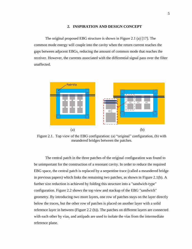
3. SIMULATION AND MEASUREMENT RESULT ANALYSIS
Based on the concept explored above, corresponding filter and PCB structures
were fabricated and simulated using a 6 layer, Megtron 6 laminate (εr ≈ 3.58, tg δ ≈ 0.004
at 10 GHz) with stackup information described in Figure 3.1. Filters with stripline and
microstrip traces are both considered. DC blocking capacitors are added when microstrip
lines are used. The filters are attached to the motherboard with a stencil and solderpaste
process. The physical dimensions of the fabricated filter are shown in Table 3.1.
(a) (b)
Figure 3.1. Stackup cross section of removable “sandwich” EBG: (a) stripline, (b)
microstrip line.
Table 3.1. A list of the physical dimensions of the fabrications of the EBG filters.
Parameters Stripline (Figure 3.2) Microstrip (Figure 3.3)
w 4.57 mm 4.57 mm
g 1.35 mm 1.31 mm
L 9.56 mm 9.56 mm
d 1.35 mm 1.31 mm
L_dieletric 0.7 mm 1.2 mm
gap 0.55 mm 0.45 mm

8
(a) (b)
(c) (d)
(e)
Figure 3.2. Removable “sandwich” EBG configuration (stripline): (a) isometric view, (b)
mother board, (c) a photograph of filter and PCB motherboard compared with one U.S.
dime (17.9mm diameter), (d) EBG patches and differential trace (e) EBG patches,
differential trace and ring.
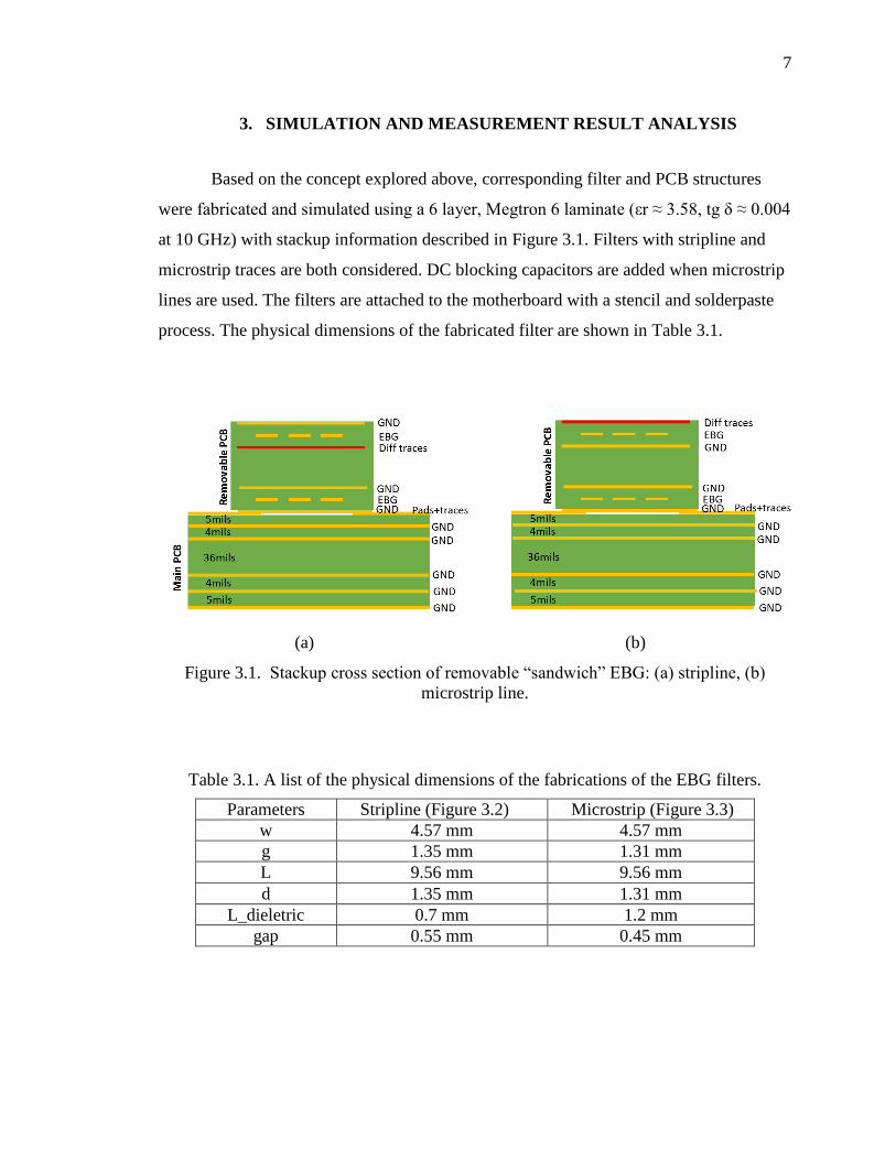
Three-dimensional, full-wave simulation models were built in CST [23] to study
the filter performance, and several views of these models are shown in Figure 3.2- Figure
3.4. The motherboard, shown in Figure 3.2 (b), is exactly the same for all cases. The
9
motherboard utilizes the top layer for differential traces and pads and the other five layers
are solid reference planes, connected by plated through-holes in each corner of the
device. Cutaway views of the removable EBG boards are shown in Figure 3.2 (d)-(e) and
Figure 3.4 (b)-(c) to provide a better understanding of the “sandwich” geometry. The
solid reference planes in the removable part, which are layers one, four and six for
stripline and layers three, four and six for microstrip, are shown in Figure 3.3. The vias
with circular antipads are used to connect the EBG patches, and the via pairs in the
rectangular antipads are used to bring the differential signals from the bottom layer to the
top or third layer of the filter board.
Figure 3.3. Top view of removable part: layer one, four and six for stripline, layer two,
four and six for microstrip line.
The manufactured motherboard features launches for a surface-mount 2.9 mm
SMK connector. These launches have been designed to minimize return and insertion
losses. The microstrip traces have 50 Ohm singled ended characteristic impedance and 85
Ohm differential characteristic impedance. The measurement and simulation results are
compared in Figure 3.5 for stripline and in Figure 3.6 for microstrip. The test boards are
measured with a calibrated 4-port VNA to observe the SCC21 and SDD21 of the
differential pair. Both measured results were de-embedded using the SFD (smart fixture
de-embedding) method [24] to remove the effect of the connector transitions. Both the
filters are designed for an 8 GHz resonance, however, due to underestimation of the
dielectric permittivity (εr ≈ 3.2 in design but εr ≈ 3.6 for manufacture), the primary
resonance shifted from 8 GHz to 7.35 GHz for stripline and to 7.45 GHz for microstrip.

10
The difference in the loss characteristics of the laminate also accounts for the magnitude
difference in SDD21 and the attenuation difference in SCC21. However, this highlights
another benefit of placing the filter in a removable part. Only the removable part needs to
be modified to adjust the filter frequency; no change to the motherboard is required. The
results indicate that both filters have 900 MHz bandwidth for 5 dB filter notch depth and
700 MHz bandwidth for 10 dB depth. In addition, adding the DC blocking capacitors to
the differential pair in the removable part will not affect the performance of differential
signaling (Figure 3.6 (b)).
(a) (b)
(c)
Figure 3.4. Removable “sandwich” EBG configuration (microstrip line): (a) isometric
view, (b) EBG patches and differential trace (c) EBG patches, differential trace and rings.
11
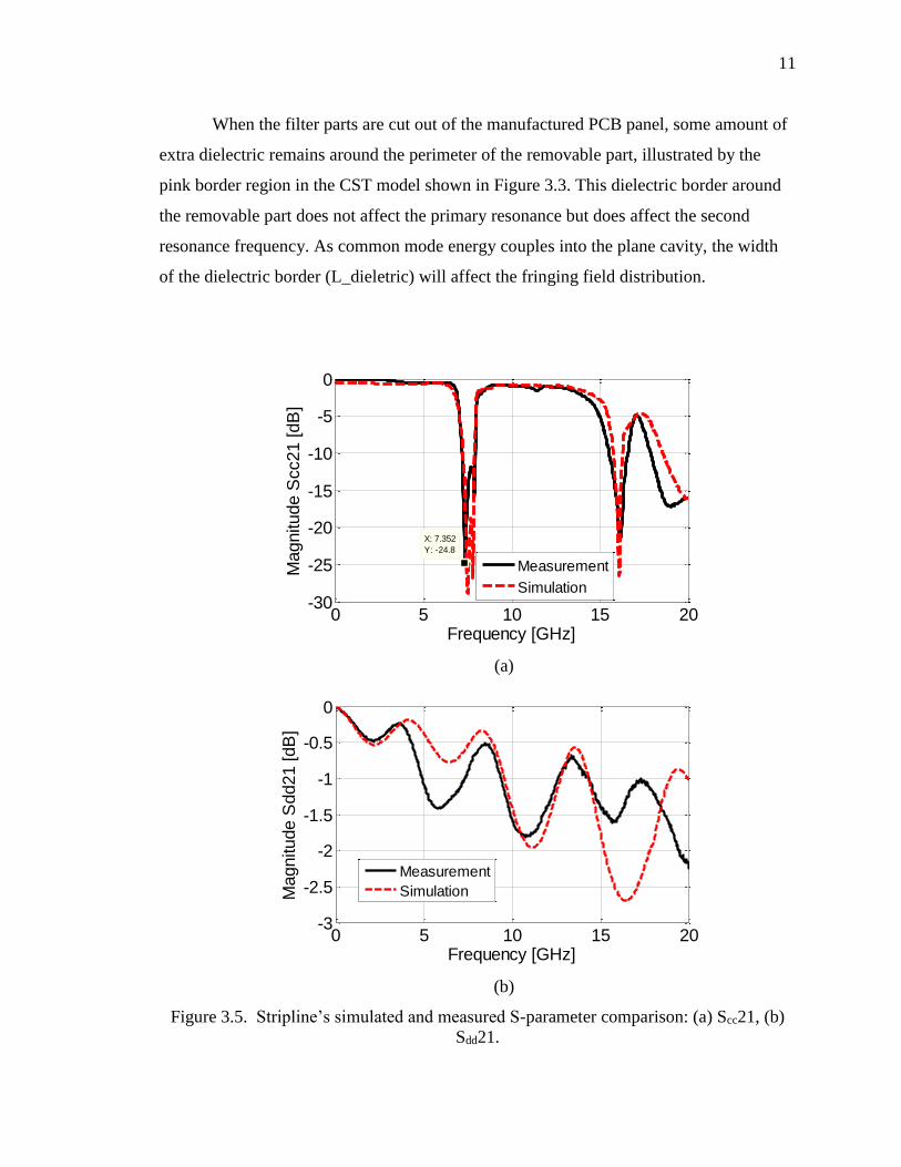
When the filter parts are cut out of the manufactured PCB panel, some amount of
extra dielectric remains around the perimeter of the removable part, illustrated by the
pink border region in the CST model shown in Figure 3.3. This dielectric border around
the removable part does not affect the primary resonance but does affect the second
resonance frequency. As common mode energy couples into the plane cavity, the width
of the dielectric border (L_dieletric) will affect the fringing field distribution.
0 5 10 15 20-30
-25
-20
-15
-10
-5
0
X: 7.352
Y: -24.8
Frequency [GHz]
Magnitude S
cc21 [dB
]
Measurement
Simulation
(a)
0 5 10 15 20-3
-2.5
-2
-1.5
-1
-0.5
0
Frequency [GHz]
Magnitude S
dd21 [dB
]
Measurement
Simulation
(b)
Figure 3.5. Stripline’s simulated and measured S-parameter comparison: (a) Scc21, (b)
Sdd21.

12
(a)
0 5 10 15 20
-4
-3
-2
-1
0
Frequency [GHz]
Magnitude S
dd21 [dB
]
Simulation
Measurement
(b)
Figure 3.6. Mcrostrip line’s simulated and measured S-parameter comparison: (a) Scc21,
(b) Sdd21.
Figure 3.7 provides the physical dimensions of the manufactured EBG patches.
Once the dielectric and stackup is determined, the filtering frequency of the removable
filter can be modified by adjusting the patch dimensions and the via locations on the
patches.
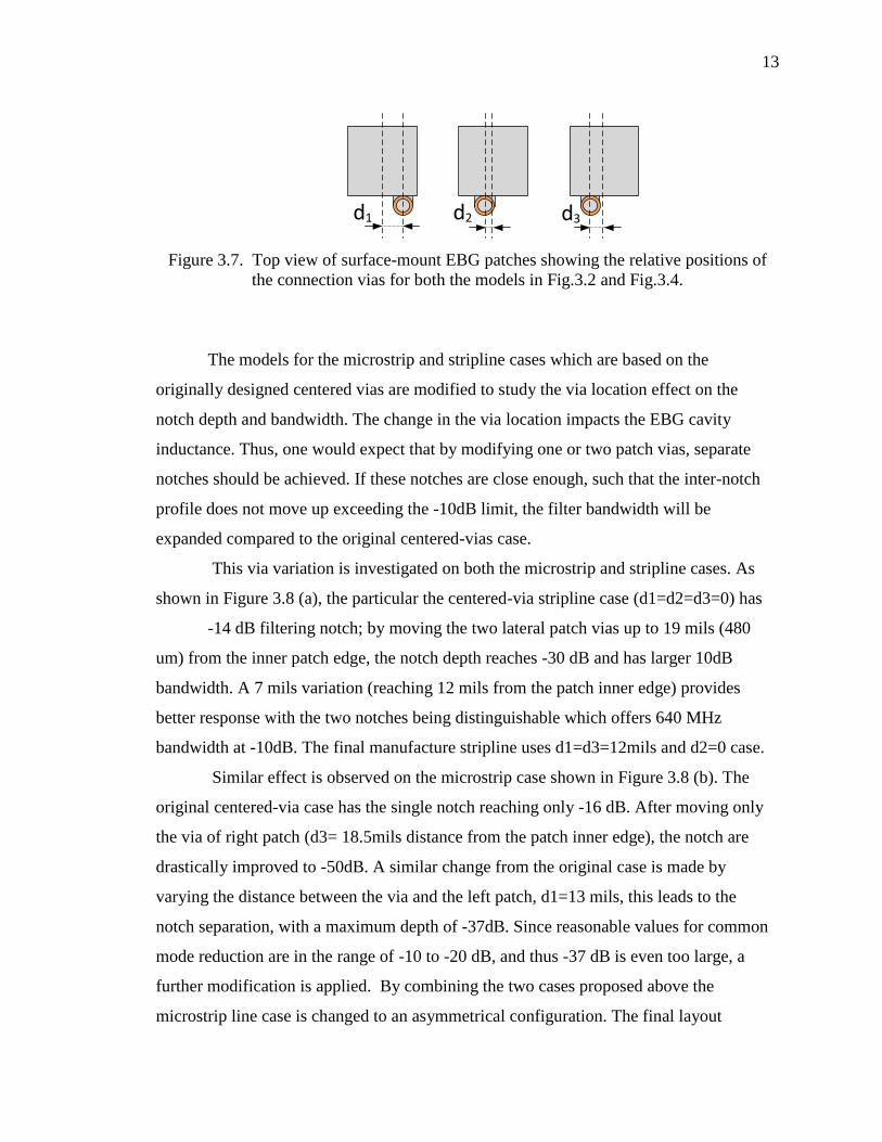
13
d1 d3d2
Figure 3.7. Top view of surface-mount EBG patches showing the relative positions of
the connection vias for both the models in Fig.3.2 and Fig.3.4.
The models for the microstrip and stripline cases which are based on the
originally designed centered vias are modified to study the via location effect on the
notch depth and bandwidth. The change in the via location impacts the EBG cavity
inductance. Thus, one would expect that by modifying one or two patch vias, separate
notches should be achieved. If these notches are close enough, such that the inter-notch
profile does not move up exceeding the -10dB limit, the filter bandwidth will be
expanded compared to the original centered-vias case.
This via variation is investigated on both the microstrip and stripline cases. As
shown in Figure 3.8 (a), the particular the centered-via stripline case (d1=d2=d3=0) has
-14 dB filtering notch; by moving the two lateral patch vias up to 19 mils (480
um) from the inner patch edge, the notch depth reaches -30 dB and has larger 10dB
bandwidth. A 7 mils variation (reaching 12 mils from the patch inner edge) provides
better response with the two notches being distinguishable which offers 640 MHz
bandwidth at -10dB. The final manufacture stripline uses d1=d3=12mils and d2=0 case.
Similar effect is observed on the microstrip case shown in Figure 3.8 (b). The
original centered-via case has the single notch reaching only -16 dB. After moving only
the via of right patch (d3= 18.5mils distance from the patch inner edge), the notch are
drastically improved to -50dB. A similar change from the original case is made by
varying the distance between the via and the left patch, d1=13 mils, this leads to the
notch separation, with a maximum depth of -37dB. Since reasonable values for common
mode reduction are in the range of -10 to -20 dB, and thus -37 dB is even too large, a
further modification is applied. By combining the two cases proposed above the
microstrip line case is changed to an asymmetrical configuration. The final layout

14
(d1=13mils, d2=3mils, d3=8mils) offered the good response in terms of notch bandwidth,
with 680 MHz bandwidth at -10dB.
6 7 8 9 10-30
-25
-20
-15
-10
-5
0
Frequency [GHz]
Magnitude S
cc21 [dB
]
d2=0, d1=d3=12mils
d1=d2=d3=0mil
d2=0, d1=d3=19mils
(a)
6 7 8 9 10-40
-30
-20
-10
0
Frequency [GHz]
Magnitude S
cc21 [dB
]
d1=13mils, d2=3mils, d3=8mils
d1=d2=d3=0
d1=13mils, d2=d3=0
d1=d2=0mil, d3=18.5mils
(b)
Figure 3.8. Simulation results coming from the different placements of the connection
vias in both the R-EBG structures: (a) stripline (model from Fig.3.2) and (b) microstrip
(model from Fig.3.4).
15
4. ANALYSIS OF TOTAL RADIATED POWER
Total radiated power (TRP) is one of the main concerns in EBG design. Due to
the discontinuities introduced by the filter, a part of the signal energy is radiated and
could cause coupling or emissions problems. In order to quantify the radiation increase of
adding a removable filter, both filters are tested in a reverberation chamber with a
common mode excitation. All the TRP measurement results in this section are normalized
to 1 Watt excitation for the comparison purposes. The far-end ports are terminated with
50 Ohm loads. Figure 4.3 compares the results of the TRP measurements. The reference
board is the differential pair on the first layer of the mother board without the removable
part. The results indicate that both stripline and microstrip line filters contribute about 23
dB more TRP at the peak around 11 GHz compared to the reference board.
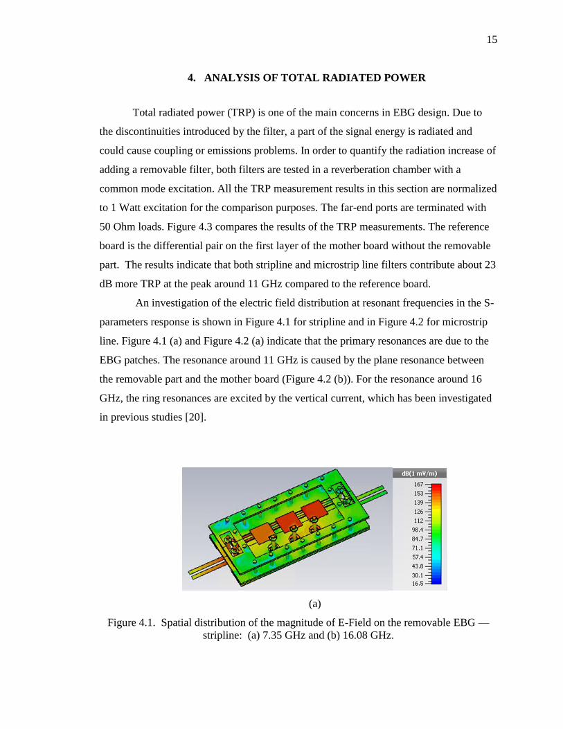
An investigation of the electric field distribution at resonant frequencies in the S-
parameters response is shown in Figure 4.1 for stripline and in Figure 4.2 for microstrip
line. Figure 4.1 (a) and Figure 4.2 (a) indicate that the primary resonances are due to the
EBG patches. The resonance around 11 GHz is caused by the plane resonance between
the removable part and the mother board (Figure 4.2 (b)). For the resonance around 16
GHz, the ring resonances are excited by the vertical current, which has been investigated
in previous studies [20].
(a)
Figure 4.1. Spatial distribution of the magnitude of E-Field on the removable EBG —
stripline: (a) 7.35 GHz and (b) 16.08 GHz.

16
(b)
Figure 4.1. Spatial distribution of the magnitude of E-Field on the removable EBG —
stripline: (a) 7.35 GHz and (b) 16.08 GHz. (cont.)
(a)
(b)
(c)
Figure 4.2. Spatial distribution of the magnitude of E-Field on the removable EBG—
microstrip line: (a) 7.45 GHz, (b) 10.08 GHz and (c) 16 GHz.

17
Figure 4.3. Measured TRP results comparison.
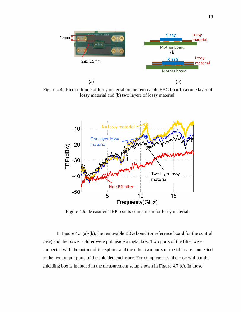
In order to reduce the impact of increased radiation, a solution of applying radio
frequency absorbing material, hereafter called ‘lossy material,’ is considered. Because the
electric field distribution suggests that the peak radiation around 11 GHz is due to the
plane resonance, we applied a picture frame of lossy material configuration around the
EBG filter. Figure 4.4 illustrates how the lossy material is applied to the filter. Two 1.5
mm gaps are cut into the picture frame lossy material to avoid degrading the differential
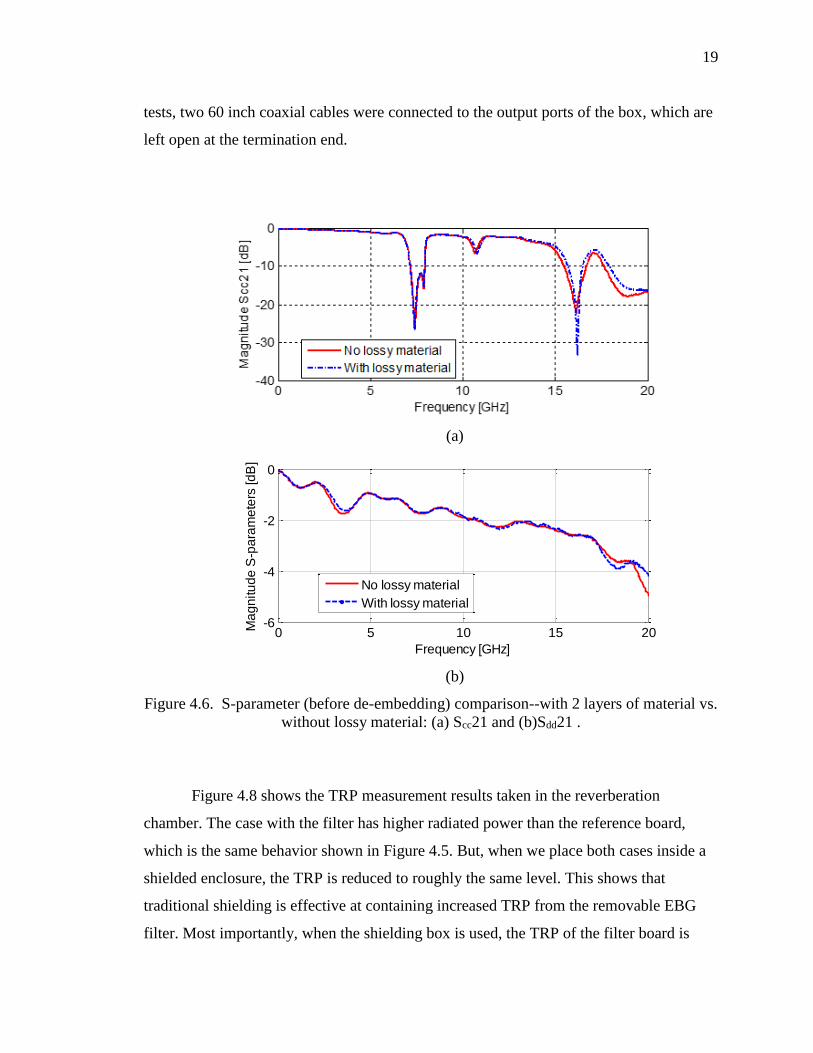
signal. The thickness of the lossy material is about 0.7 mm. Figure 4.6 shows the lossy
material has a negligible effect on the differential signal and a very small impact on the
primary resonance of the common mode signal. But for the TRP results comparison
shown in Figure 4.5, about 6 dB reduction can be observed at 11 GHz when one layer of
lossy material is applied. In addition, about 5 dB more reduction is achieved when using
two layers of lossy material. The TRP was unaffected below 10 GHz because the plane
resonance was not a dominant radiation mechanism at those frequencies.
The second method to reduce the TRP impact of the filter is to put the filter into a
shielded enclosure. Most printed circuit boards with high-speed differential interfaces are
placed inside shielded enclosures, so this method is very relevant for practical
applications.
18
(a) (b)
Figure 4.4. Picture frame of lossy material on the removable EBG board: (a) one layer of
lossy material and (b) two layers of lossy material.
Figure 4.5. Measured TRP results comparison for lossy material.
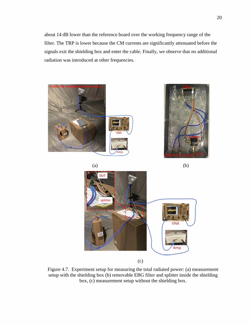
In Figure 4.7 (a)-(b), the removable EBG board (or reference board for the control
case) and the power splitter were put inside a metal box. Two ports of the filter were
connected with the output of the splitter and the other two ports of the filter are connected
to the two output ports of the shielded enclosure. For completeness, the case without the
shielding box is included in the measurement setup shown in Figure 4.7 (c). In those
19
tests, two 60 inch coaxial cables were connected to the output ports of the box, which are
left open at the termination end.
(a)
0 5 10 15 20-6
-4
-2
0
Frequency [GHz]
Ma
gn
itu
de
S-p
ara
me
ters
[d
B]
No lossy material
With lossy material
(b)
Figure 4.6. S-parameter (before de-embedding) comparison--with 2 layers of material vs.
without lossy material: (a) Scc21 and (b)Sdd21 .
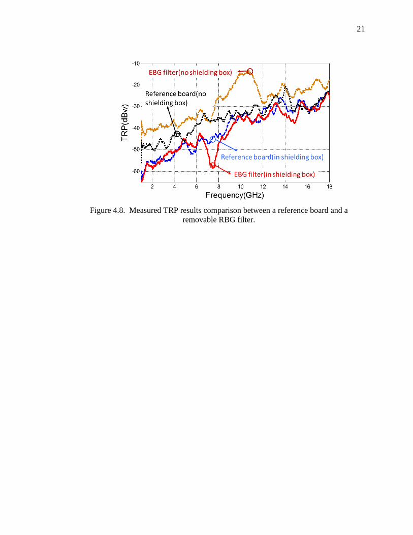
Figure 4.8 shows the TRP measurement results taken in the reverberation
chamber. The case with the filter has higher radiated power than the reference board,
which is the same behavior shown in Figure 4.5. But, when we place both cases inside a
shielded enclosure, the TRP is reduced to roughly the same level. This shows that
traditional shielding is effective at containing increased TRP from the removable EBG
filter. Most importantly, when the shielding box is used, the TRP of the filter board is
20
about 14 dB lower than the reference board over the working frequency range of the
filter. The TRP is lower because the CM currents are significantly attenuated before the
signals exit the shielding box and enter the cable. Finally, we observe that no additional
radiation was introduced at other frequencies.
(a) (b)
(c)
Figure 4.7. Experiment setup for measuring the total radiated power: (a) measurement
setup with the shielding box (b) removable EBG filter and splitter inside the shielding
box, (c) measurement setup without the shielding box.
21
Figure 4.8. Measured TRP results comparison between a reference board and a
removable RBG filter.
22
5. CONCLUSION
A removable “sandwich” EBG-based common mode filter was designed,
manufactured, and tested in this paper. The advantages of this filter are numerous. It can
be installed, substituted and removed by the typical soldering assembly process, which is
easy to meet the filter needs of PCB differential link designers at any stage of the design
process. The device is a viable answer to the presence of unexpected common mode
noise and even the changing of data rates on particular lines which would require filtering
at different target frequencies. The external dimensions of the removable filter remain
unchanged in order to fit the fixed filter area allocated on the board. The total radiated
power of the removable filter component was studied, and we found that TRP increases
when the filter is used. Two methods are discussed to reduce the added TRP. One way is
to add picture-frame-shaped lossy material around this filter to suppress the unwanted
TRP without affecting the differential signals. Another is to put the filter inside a shielded
enclosure, which prevents the increased TRP of the filter from radiating outside the box
and reduces the system-level emissions due to the cable or its attachment to the enclosure
by suppressing the common mode currents over the designed filter bandwidth. For
shielded systems with radiated emissions issues being driven by the common mode
currents on cables, backshells, or cable housings, this removable EBG-based filter can be
an effective remedy.
23
REFERENCES
[1] S. Shahparnia and O. M. Ramahi, "Electromagnetic interference (EMI) reduction
from printed circuit boards (PCB) using electromagnetic bandgap structures," in IEEE
Trans. Electromagn. Compat., vol. 46, no. 4, pp. 580–587, Nov. 2004.
[2] B. Archambeault, S. Connor, and J. Diepenbrock, "EMI emissions from mismatch in
high-speed differential signal trace and cables," in Proc. IEEE Int. Symp.
Electromagn. Compat., Hawaii, Jul. 2007, pp. 1-6.
[3] G. Li, W. Qian, A. Radchenko, G. Hess, R. Hoeckele, P. Jalbert, T. Van Doren, D.
Pommerenke, and D. Beetner, “Estimating the radiated emissions from cables
attached to a switching power supply in a MIL-STD 461 test,” in IEEE Int. Symp.
EMC, Denver, CO, pp. 626-631, 2013.
[4] Z. Yan; Y. Xiong; W. Yu; Y. Wang, "An Improved Miniaturized Three-Layer
Embedded Electromagnetic Bandgap Structure," in IEEE Trans. Antennas Propag, pp.
2832-2837, May 2014.
[5] G.-H. Shiue, C.-L. Hsu, C.-L. Yeh, and C.-F. Hsu, "A comprehensive investigation of
a common-mode filter for gigahertz differential signals using quarter-wavelength
resonators", in IEEE Trans. Compon., Packag., Manuf. Technol., vol. 4, no. 1, pp.
134–144, Jan. 2014.
[6] Q. Liu; G. Li.; V. Khilkevich; D. Pommerenke, "Common-Mode Filters With
Interdigital Fingers for Harmonics Suppression and Lossy Materials for Broadband
Suppression," in IEEE Trans. Electromagn. Compat., vol.57, no.6, pp.1740-1743,
Dec. 2015.
[7] S. Wu.; C. Tsai; T. Wu; T. Itoh, "A Novel Wideband Common-Mode Suppression
Filter for Gigahertz Differential Signals Using Coupled Patterned Ground Structure,"
in Microwave Theory and Techniques, IEEE Trans. on , vol.57, no.4, pp.848,855,
Apr. 2009.
[8] F.de Paulis, A. Orlandi, "Signal Integrity Analysis of Single-Ended and Differential
Striplines in Presence of EBG Planar Structures", in IEEE Microwave and Wireless
Components Letters, vol. 19, nr. 9, Sep. 2009.
[9] F. De Paulis, L. Raimondo, D. Di Febo, B. Archambeault, S. Connor, A. Orlandi,
"Experimental Validation of Common-Mode Filtering Performances of Planar
Electromagnetic Band-gap Structures", in Proc. of 2010 IEEE Symposium on
Electromagnetic Compatibility, Fort Lauderdale, FL, USA, 25-30 Jul. 2010.

24
[10] F. De Paulis, L. Raimondo, S. Connor, B. Archambeault, A. Orlandi, "Design of a
Common Mode Filter by using Planar Electromagnetic Bandgap Structures", in
IEEE Trans. on Advanced Packaging, vol. 33, n. 44, Nov. 2010.
[11] F. De Paulis, L. Raimondo, D. Di Febo, A. Orlandi, "Trace Routing Strategies for
Improving Common Mode Filter Performances in High Speed Digital Differential
Interconnects", in Proc. of 15th IEEE Workshop on Signal Propagation on
Interconnects, Naples, Italy, May 08-11, 2011.
[12] F. De Paulis, L. Raimondo, S. Connor, B. Archambeault, A. Orlandi, "Compact
Configuration for Common Mode Filter Design based on Planar Electromagnetic
Bandgap Structures", in IEEE Trans. on Electromagn. Compat. vol. 54, no. 3, pp.
646-655, June 2012.
[13] F. de Paulis, B. Archambeault, M. H. Nisanci, S. Connor, and A. Orlandi,
"Miniaturization of Common Mode Filter Based on EBG Patch Resonance", in Proc.
IEC DesignCon 2012, January 30-February 2, 2012, Santa Clara, USA.
[14] M.H. Nisanci, F.De Paulis, A.Orlandi, B. Archambeault, S.Connor, "Optimum
Geometrical parameters for the EBG-Based Common Mode Filter Design", in Proc.
of 2012 IEEE Symposium on Electromagn. Compat., Pittsburgh, PA, USA, 5-10
August, 2012.
[15] X. Gu, R. Rimolo-Donadio, Y. Kwark, C. Baks, F. de Paulis, M. H. Nisanci, A.
Orlandi, B. Archambeault, S. Connor, Design and "Experimental Validation of
Compact Common Mode Filter Based on EBG Technology", in Proc. of IEC
DesignCon 2013, January 28-31, 2013, Santa Clara, USA.
[16] F. de Paulis, M. H. Nisanci, A. Orlandi, X. Gu, R. Rimolo-Donadio, Y. Kwark, C.
Baks, B. Archambeault, S. Connor, "Experimental Validation of an 8 GHz EBG
Based Common Mode Filter and Impact on Manufacturing Uncertainties", in Proc.
of IEEE Int. Symp. on EMC, August 5-9, 2013, Denver, CO, USA.
[17] C. Olivieri, F. de Paulis, A. Orlandi, S. Connor, B. Archambeault, "Miniaturization
Approach for EBG-Based Common Mode Filter and Interference Analysis", IEEE
Int. Symp. on EMC, March 15-20, 2015, Santa Clara CA, USA.
[18] F. de Paulis, M. Cracraft, D.Di Febo, H.M.Nisanci, S. Connor, B. Archambeault, A.
Orlandi, "EBG-based common mode microstrip and stripline filters: experimental
investigation of performances and crosstalk", IEEE Trans. on Electromagn. Compat.,
early access article, May 2015.
[19] F. de Paulis, M. Cracraft, C. Olivieri, S. Connor, A. Orlandi, B. Archambeault,
"EBG-Based Common Mode Stripline Filters: Experimental Investigation on
Interlayer Crosstalk", IEEE Trans. on Electromagn. Compat., vol. 57, nr. 6, pp.
1416-1424, Dec. 2015.
25
[20] M.A. Varner, F. de Paulis, A. Orlandi, S. Connor, M. Cracraft, B. Archambeault,
H.Nisanci, D. di Febo, "Removable EBG-Based Common Mode Filter for High
Speed Signaling: Design and Experimental Validation", IEEE Trans. on
Electromagn. Compat., Special Issue on the 2014 IEEE International Symposium on
EMC, vol. 57, nr. 4, pp. 672-679, Aug. 2015.
[21] L. Raimondo, F. De Paulis, A. Orlandi, "A Simple and Efficient Design Procedure
for Planar Electromagnetic Band-gap Structures on Printed Circuit Boards", IEEE
Trans. on Electromagn. Compat., Vol. 53, nr. 2, pp. 482-490, May 2011.
[22] F. De Paulis and A. Orlandi, "Accurate and efficient analysis of planar
electromagnetic band-gap structures for power bus noise mitigation in the GHz
band", in Proc. of Electromagnetics Research B, Vol. 37, 59-80, 2012.
[23] Computer Simulation Technology, CST STudiuo Suite 2015, www.cst.com.
[24] X. Ye; J. Fan; B. Chen; J. Drewniak, Q. Chen, "Accurate characterization of PCB
transmission lines for high speed interconnect," Electromagn. Compat.(APEMC),
2015 Asia-Pacific Symp. on , vol., no., pp.16-19, 26-29 May 2015.

26
II. COMMON-MODE FILTERS WITH INTERDIGITAL FINGERS FOR
HARMONICS SUPPRESSION AND LOSSY MATERIALS FOR BROADBAND
SUPPRESSION
Qian Liu, Student Member, IEEE, Guanghua Li, Student Member, IEEE, Victor
Khilkevich, Member, IEEE, David Pommerenke, Fellow, IEEE
ABSTRACT
Common-mode (CM) noise on differentialmicrostrip lines can be suppressed by
PCB-embedded filters. These filters use resonating or broadband structures such that only
the field from the CM signal couples to them. Based on a quarter-wavelength resonator, a
new PCB filter is designed having an electrical size of only 0.15 λ × 0.065 λ, where λ is
the effective wavelength in the CM filter. Its interdigital structure is also capable of
suppressing higher order harmonics of the CM signal and can be used for USB 3.0 to
mitigate electromagnetic interference. Further, a novel broadband suppression structure is
described that uses magnetically lossy material to suppress the CM signal from 4.6 to 20
GHz without strongly affecting the intended differential signal.
Index Terms— Broadband filter, common-mode filter, differential signal, quarter-
wavelength, narrowband filter.
27
1. INTRODUCTION
Common mode (CM) noise is caused by an imbalanced differential signal path,
which in turn causes electromagnetic interference problems [1]. These problems can be
mitigated by suppressing the CM noise using CM filters embedded in the signal path.
These filters have been widely designed and analyzed using defected ground structures
(DGS) and electromagnetic bandgap (EBG) structures [2]–[5]. The 0.4 λ × 0.16 λ (0.064
λ2) (where λ is the effective wavelength in the CM filter) size of the EBG structure was
achieved by removing a central patch in a 5-layer stackup [3]. The dimensions were
further decreased to 0.21 λ × 0.21 λ (0.044 λ2) by introducing a C-shaped patterned
ground structure found in [6] and decreased to 0.026 λ2 by using coupled synthesized
microstrip line and modified mushroom resonators as found in [7]. Furthermore, a
quarter-wavelength resonator was used in the filter design (electrical size 0.01 λ × 0.25
λ=0.0025 λ2) in [8] for an even smaller dimension compared to DGS and EBG structures.
According to the suppression bandwidth, the CM filter can be subdivided into
narrowband and broadband filters. The narrow- band filter suppresses signals around a
single frequency (and maybe its harmonics). The wideband filter has a much broader
stopband, which can be achieved by combining several narrow- band filters, but at the
expense of occupied area. High-speed digital signals often contain harmonics of the clock
frequency. So a compact CM filter that can suppress a single frequency as well as the
harmonics of that frequency is desirable.
In order to further decrease the filter’s dimension, this paper introduces a CM
filter with an electrical size of only 0.15 λ ×0.065 λ (0.0098 λ2), based on an interdigital
quarter-wavelength resonator. This filter has the additional advantage of suppressing CM
noise at both the odd and even harmonic frequencies of the resonator. Additionally, this
paper discusses a new way to suppress broadband CM noise up to 20 GHz by overlaying
magnetically lossy material on a metal patch above a PCB-based filter.
28
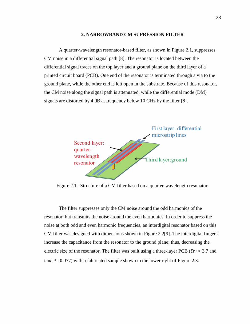
2. NARROWBAND CM SUPRESSION FILTER
A quarter-wavelength resonator-based filter, as shown in Figure 2.1, suppresses
CM noise in a differential signal path [8]. The resonator is located between the
differential signal traces on the top layer and a ground plane on the third layer of a
printed circuit board (PCB). One end of the resonator is terminated through a via to the
ground plane, while the other end is left open in the substrate. Because of this resonator,
the CM noise along the signal path is attenuated, while the differential mode (DM)
signals are distorted by 4 dB at frequency below 10 GHz by the filter [8].
Figure 2.1. Structure of a CM filter based on a quarter-wavelength resonator.
The filter suppresses only the CM noise around the odd harmonics of the
resonator, but transmits the noise around the even harmonics. In order to suppress the
noise at both odd and even harmonic frequencies, an interdigital resonator based on this
CM filter was designed with dimensions shown in Figure 2.2[9]. The interdigital fingers
increase the capacitance from the resonator to the ground plane; thus, decreasing the
electric size of the resonator. The filter was built using a three-layer PCB (Ɛr ≈ 3.7 and
tanδ ≈ 0.077) with a fabricated sample shown in the lower right of Figure 2.3.
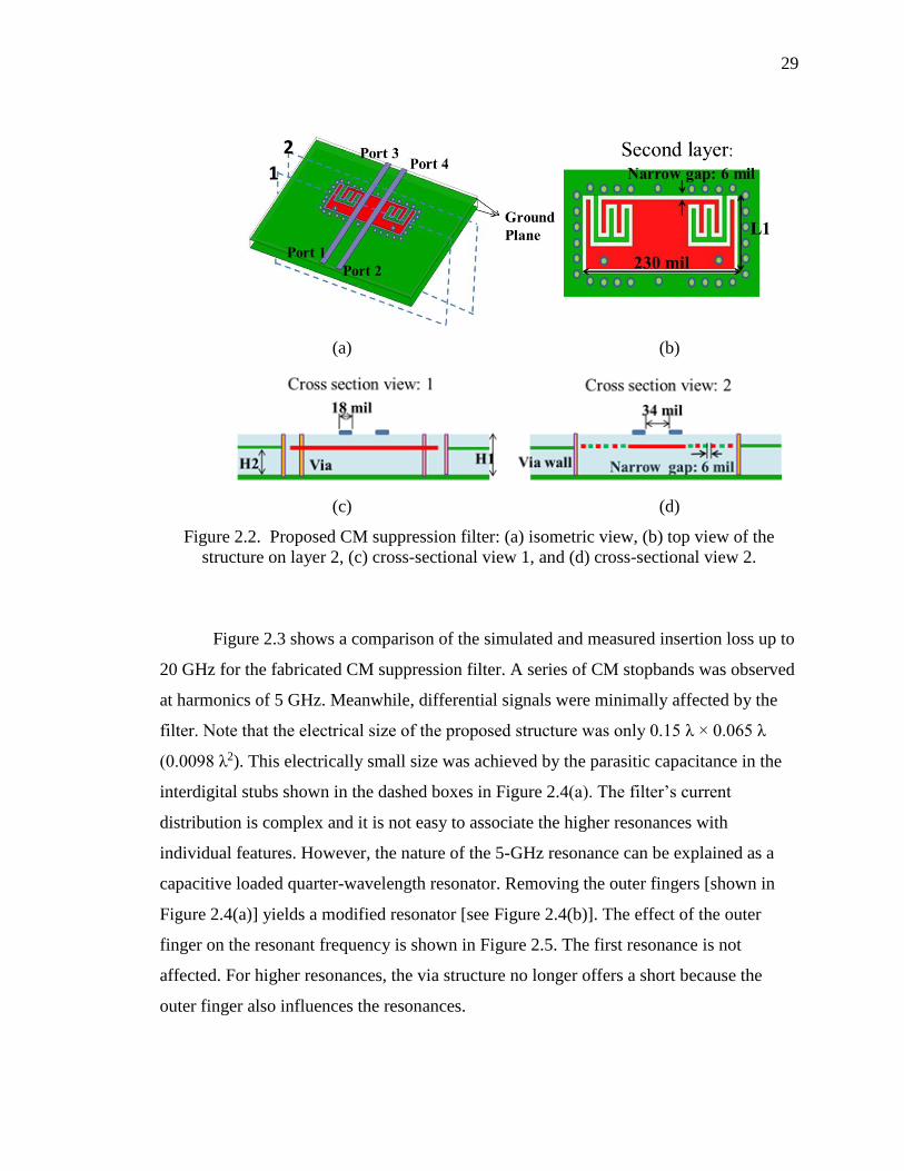
29
(a) (b)
(c) (d)
Figure 2.2. Proposed CM suppression filter: (a) isometric view, (b) top view of the
structure on layer 2, (c) cross-sectional view 1, and (d) cross-sectional view 2.
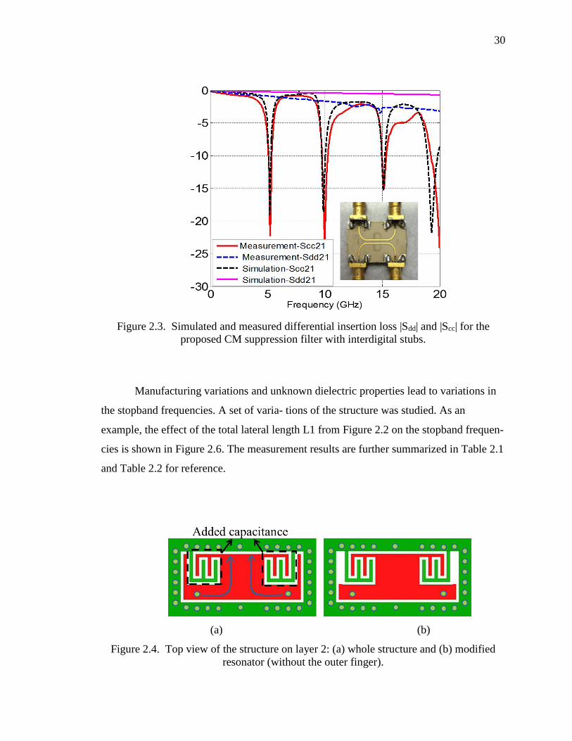
Figure 2.3 shows a comparison of the simulated and measured insertion loss up to
20 GHz for the fabricated CM suppression filter. A series of CM stopbands was observed
at harmonics of 5 GHz. Meanwhile, differential signals were minimally affected by the
filter. Note that the electrical size of the proposed structure was only 0.15 λ × 0.065 λ
(0.0098 λ2). This electrically small size was achieved by the parasitic capacitance in the
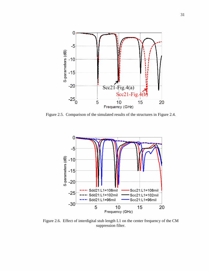
interdigital stubs shown in the dashed boxes in Figure 2.4(a). The filter’s current
distribution is complex and it is not easy to associate the higher resonances with
individual features. However, the nature of the 5-GHz resonance can be explained as a
capacitive loaded quarter-wavelength resonator. Removing the outer fingers [shown in
Figure 2.4(a)] yields a modified resonator [see Figure 2.4(b)]. The effect of the outer
finger on the resonant frequency is shown in Figure 2.5. The first resonance is not
affected. For higher resonances, the via structure no longer offers a short because the
outer finger also influences the resonances.
30
Figure 2.3. Simulated and measured differential insertion loss |Sdd| and |Scc| for the
proposed CM suppression filter with interdigital stubs.
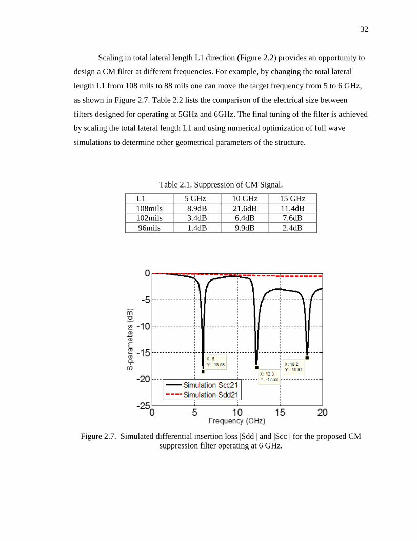
Manufacturing variations and unknown dielectric properties lead to variations in
the stopband frequencies. A set of varia- tions of the structure was studied. As an
example, the effect of the total lateral length L1 from Figure 2.2 on the stopband frequen-
cies is shown in Figure 2.6. The measurement results are further summarized in Table 2.1
and Table 2.2 for reference.
(a) (b)
Figure 2.4. Top view of the structure on layer 2: (a) whole structure and (b) modified
resonator (without the outer finger).
31
Figure 2.5. Comparison of the simulated results of the structures in Figure 2.4.
Figure 2.6. Effect of interdigital stub length L1 on the center frequency of the CM
suppression filter.
32
Scaling in total lateral length L1 direction (Figure 2.2) provides an opportunity to
design a CM filter at different frequencies. For example, by changing the total lateral
length L1 from 108 mils to 88 mils one can move the target frequency from 5 to 6 GHz,
as shown in Figure 2.7. Table 2.2 lists the comparison of the electrical size between
filters designed for operating at 5GHz and 6GHz. The final tuning of the filter is achieved
by scaling the total lateral length L1 and using numerical optimization of full wave
simulations to determine other geometrical parameters of the structure.
Table 2.1. Suppression of CM Signal.
L1 5 GHz 10 GHz 15 GHz
108mils 8.9dB 21.6dB 11.4dB
102mils 3.4dB 6.4dB 7.6dB
96mils 1.4dB 9.9dB 2.4dB
Figure 2.7. Simulated differential insertion loss |Sdd | and |Scc | for the proposed CM
suppression filter operating at 6 GHz.

33
Table 2.2. Comparison of target frequency and electrical size.
First resonant frequency Electrical length
5 GHz 0.15 λ × 0.065 λ
6 GHz 0.17 λ × 0.063 λ

34
3. BROADBAND CM SUPPRESSION FILTER
The CM suppression filter in Section II suffers from the draw- back of only
suppressing CM noise in narrow frequency bands, which may be insufficient to ensure
signal quality for a signal path under the influence of broadband noise. This issue can be
solved by cascading several narrowband filters with differ- ent stopband frequencies, but
at the cost of increased size on the PCB. Another method is to dissipate the CM energy in
the signal path with broadband lossy materials, such that the broadband CM noise cannot
propagate along the path efficiently. Mean- while, the energy of the DM signals is only
slightly absorbed by the lossy materials.
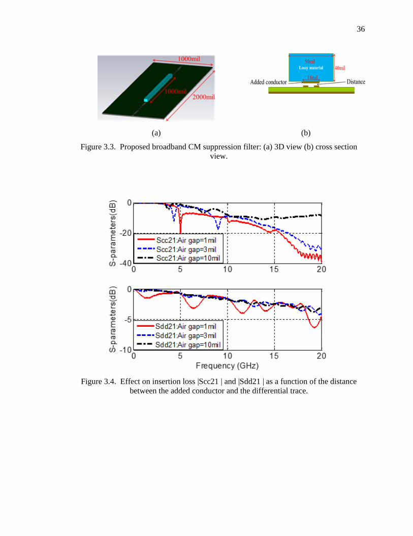
The broadband CM suppression filter described in this section utilizes a PCB with
overlaid magnetically lossy material and is illustrated in Figure 3.1. A thin copper patch
was placed above the differential trace and the lossy material was placed directly above
this conductor. According to the conceptual field distributions illustrated in Figure 3.1,
fields from the CM current will penetrate the lossy material, while the fields from the DM
current will be contained underneath the patch. This field be- havior was further validated
by the simulated field distributions with and without the additional copper patch for both
DM and CM excitations. These results suggest that lossy material placed above the patch
will significantly affect the CM noise, but not the DM signals.
(a) (b)
Figure 3.1. Conceptual field distribution from: (a) DM signal and (b) CM noise in a
differential trace with overlaid metal and additional lossy material.
35
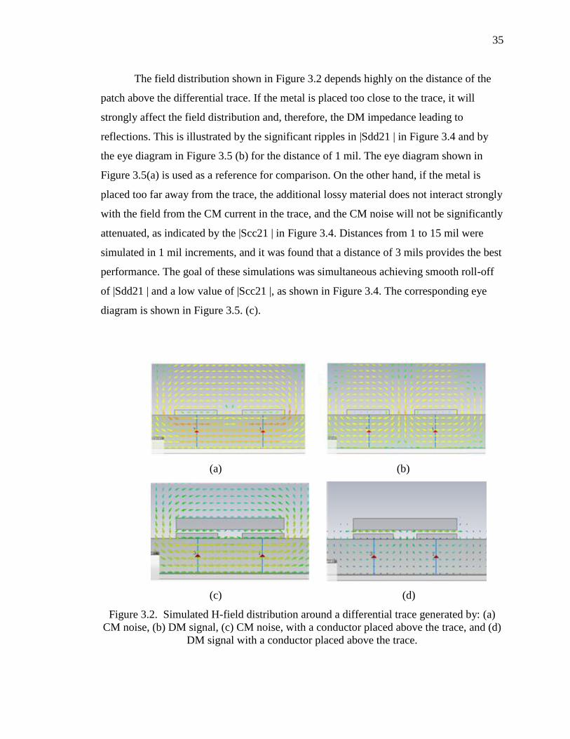
The field distribution shown in Figure 3.2 depends highly on the distance of the
patch above the differential trace. If the metal is placed too close to the trace, it will
strongly affect the field distribution and, therefore, the DM impedance leading to
reflections. This is illustrated by the significant ripples in |Sdd21 | in Figure 3.4 and by
the eye diagram in Figure 3.5 (b) for the distance of 1 mil. The eye diagram shown in
Figure 3.5(a) is used as a reference for comparison. On the other hand, if the metal is
placed too far away from the trace, the additional lossy material does not interact strongly
with the field from the CM current in the trace, and the CM noise will not be significantly
attenuated, as indicated by the |Scc21 | in Figure 3.4. Distances from 1 to 15 mil were
simulated in 1 mil increments, and it was found that a distance of 3 mils provides the best
performance. The goal of these simulations was simultaneous achieving smooth roll-off
of |Sdd21 | and a low value of |Scc21 |, as shown in Figure 3.4. The corresponding eye
diagram is shown in Figure 3.5. (c).
(a) (b)
(c) (d)
Figure 3.2. Simulated H-field distribution around a differential trace generated by: (a)
CM noise, (b) DM signal, (c) CM noise, with a conductor placed above the trace, and (d)
DM signal with a conductor placed above the trace.
36
(a) (b)
Figure 3.3. Proposed broadband CM suppression filter: (a) 3D view (b) cross section
view.
Figure 3.4. Effect on insertion loss |Scc21 | and |Sdd21 | as a function of the distance
between the added conductor and the differential trace.

37
(a) (b)
(c) (d)
Figure 3.5. Simulated eye diagrams of a differential trace: (a) without the overly- ing
metal and the additional lossy material as a reference, and with the overlying metal and
the additional lossy material for a distance of (b) 1 mil, (c) 3 mils, and (d) 10 mils.
38
4. COMBINED CM SUPPRESSION FILTER
The bandwidth of the proprietary lossy material-based filter in Section III is
limited partly by the bandwidth of the over- lying lossy material (Ɛr ≈ 17 and tan δƐ≈
0.004; µr 1.2 and tan δµ ≈ 1 at 10 GHz). The lossy material cannot help suppress CM
noise at frequencies below the material usable frequency. For example, the magnitude of
|Scc21 | is greater than –5 dB from 5 to 8 GHz (as shown in Figure 3.4.). One can suppress
the CM noise in this frequency range by combining a quarter- wavelength resonator-
based filter with the lossy material-based filter in Section III, leading to an even broader
bandwidth.
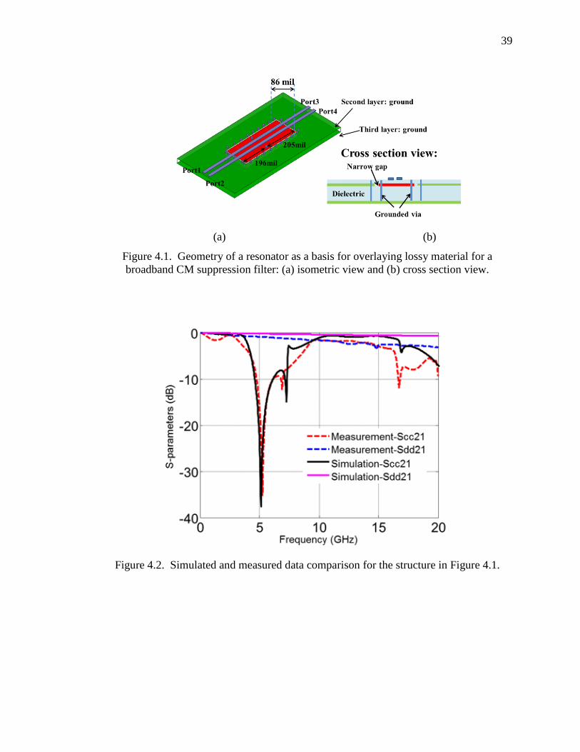
The A quarter-wavelength resonator-based filter, shown in Figure 4.1, was built
using the same setup as in Figure 2.2. The resonator had two open-ended stubs sharing
two vias terminated to the ground plane. The 196-mils-long stub created a stop band at
5.2 GHz, while the 205-mils-long stub created a second stop- band at 4.8 GHz. The
simulation and measurement results are shown in Figure 4.2. As expected, this filter
cannot suppress CM noise at frequencies between 8 and 16 GHz.
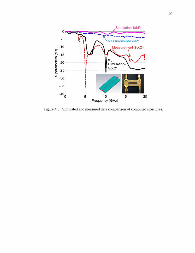
A piece of 1000-mils-long and 50-mils-wide proprietary magnetic-lossy material
was placed 3.4 mils above the quarter- wavelength resonator-based filter, shown in the
bottom right of Figure 4.3., using the same method of placement as described in the
previous section. A 3.4-mil-thick paper masking tape was used as a spacer to sustain
between the lossy material and the filter. Both simulated and measured results shown in
Figure 4.3 indicate a smaller |Scc21 | than that shown in Figure 3.4, while keeping |Sdd21 |
below –7 dB up to 20 GHz. This validated the method of combining different structures
for broadening the filter bandwidth.
39
(a) (b)
Figure 4.1. Geometry of a resonator as a basis for overlaying lossy material for a
broadband CM suppression filter: (a) isometric view and (b) cross section view.
Figure 4.2. Simulated and measured data comparison for the structure in Figure 4.1.
40
Figure 4.3. Simulated and measured data comparison of combined structures.

41
5. CONCLUSION
A narrowband CM suppression filter based on an inter-digital resonator with
electrical area as small as 0.0098 λ2 was designed. The filter is able to suppress CM noise
at both odd and even harmonics of the fundamental resonance frequency. Additionally, a
broadband CM filter capable of effectively suppressing broadband noise in the frequency
range from 4.6 GHz to 20 GHz was constructed by overlaying lossy materials on a piece
of metal placed above a quarter-wavelength resonator.
42
REFERENCES
[1] B. Archambeault, S. Connor, and J. Diepenbrock, “EMI emissions from mismatch in
high-speed differential signal trace and cables,” in Proc. IEEE Int. Symp. Trans.
Electromagn. Compat., Hawaii, Jul. 2007, pp. 1-6.
[2] Z. Yan; Y. Xiong; W. Yu; Y. Wang, "An Improved Miniaturized Three-Layer
Embedded Electromagnetic Bandgap Structure," IEEE Trans. Antennas Propag, pp.
2832-2837, May 2014.
[3] C. Olivieri, F. de Paulis, S. Connor, B. Archambeault, and A. Orlandi, "Miniaturization
approach for EBG-based common mode filter and interference analysis," IEEE Symp.
EMC, Santa Clara,CA, pp. 91-96, March. 2015.
[4] Y. Pang, Z. Feng, "A compact common-mode filter for GHz differential signals using
defected ground structure and shorted microstrip stubs," 2012 Int. Conference, Microw.
and Millimeter Wave Technology , May 2012, pp. 1-4.
[5] W. Liu; C. Tsai, T. Han, and T. Wu, "An Embedded Common-Mode Suppression Filter
for GHz Differential Signals Using Periodic Defected Ground Plane," IEEE Trans.
Microw. Wireless Compon. Lett., pp. 248-250, Apr. 2008.
[6] T. Weng, C. Tsai, C. Chen, D. Han and T. Wu, "Synthesis Model and Design of a
Common-Mode Bandstop Filter (CM-BSF) With an All-Pass Characteristic for High-
Speed Differential Signals," IEEE Trans. Microw. Theory Tech, Aug. 2014.
[7] B. Su; T. Ma, "Miniaturized Common-Mode Filter Using Coupled Synthesized Lines
and Mushroom Resonators for High-Speed Differential Signals," IEEE Trans. Microw.
Wireless Compon. Lett., vol.25, no.2, pp.112,114, Feb. 2015.
[8] G. Shiue, C Hsu, C. Yeh, and C. Hsu, "A Comprehensive Investigation of a Common-
Mode Filter for Gigahertz Differential Signals Using Quarter-Wavelength Resonators,"
IEEE Trans. Compon., Packag.,Manuf. Technol, vol. 4, no. 1, pp. 134–144, Jan. 2014.
[9] Q. Liu, S. Xu, and D. Pommerenke, "PCB structures for common mode suppression on
differential microstrip lines," in IEEE Int. Symp. EMC, Raleigh, NC, Aug. 2014,
pp.533-537.

43
III. PCB STRUCTURE FOR COMMON MODE SUPPRESSION ON
DIFFEREITNAIL MICROSTRIP LINES
Qian Liu, Student Member, IEEE, Shuai Xu, Member, IEEE, David Pommerenke,
Fellow, IEEE
ABSTRACT
Common mode noise on differential microstrip lines can be suppressed by PCB
embedded filters. These filters are basically resonators, and only the common mode
signal can couple to them. Though such structure suppress common mode signal only in
narrow bands because of the resonant nature, they can be combined to produce broadband
filtering effect. The dimension of such filters could be further reduced by adding lumped
elements. In this paper, design principles of the PCB filters are given, and examples are
given to demonstrate these rules. At last, a new PCB filter structure is proposed with an
electrical size of only 0.04λ×0.067λ which is capable of suppressing the higher order
harmonics of common mode signal.
Index Terms— Common mode filter, differential signal, quarter-wavelength,
lower resonant frequency.

44
1. INTRODUCTION
All differential interfaces will carry common mode signals. Common mode
signals could originate from drivers, non-identical rise and fall times, unbalanced traces
or skew, etc. Common mode signals may couple to structures capable of radiation, such
as the outside of cable shields and enclosures, causing EMI problems. These problems
can be solved by improving the driver, removing the structures that cause differential to
common mode conversion, filtering the common mode current, or reducing the coupling
to structures capable of radiating the signal. This paper focuses on structures that filter
common mode currents on differential traces.
Common mode suppression on differential signals can be subdivided into four
classes: active compensation of common mode, which is more suitable for lower
frequencies; common mode compensation structures; discrete components for
suppression, such as common mode chokes; and common mode suppression structures,
integrated into printed circuit boards (PCBs). An example of common mode
compensation structures is bended differential lines using compensation capacitors [1]
and/or inductors [2] so as to improve the symmetry of the differential pairs. The third
class of filters is discrete component such as common mode chokes. A common mode
choke maintains the differential mode impedance by creating a highly coupled
differential pair that is wound into a coil. Ferrite core might be added to the coil to
increase the inductance at lower frequencies. Since a common mode choke is discrete
broadband component, it cannot be characterized by its electrical size. There are some
other common mode chokes that are manufactured using low-temperature co-fired
ceramic (LTCC) substrates with a small size of 1.2 mm ×2.0 mm [3]; these common
mode chokes are able to provide common mode suppression up to 5GHz. So far, it is still
difficult to find common mode chokes on-board that perform well above 5 GHz. The
fourth class of filters are PCB based structures. These resonant structures have been
designed to only disturb the common mode field distribution on the differential traces
without significantly affecting the differential mode. These structures have been
researched well in [4]-[8] by Tzong-Lin Wu’s group. Usually the dimension of the
resonant structures used for common mode suppression depends on the operating
45
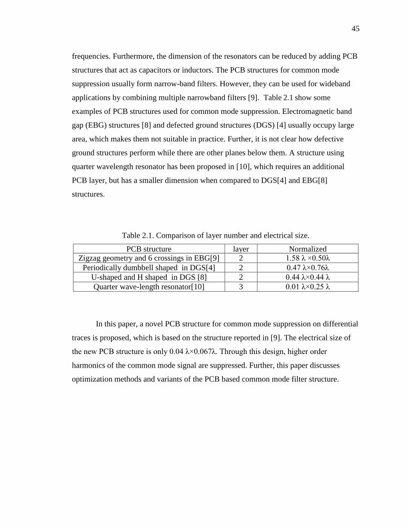
frequencies. Furthermore, the dimension of the resonators can be reduced by adding PCB
structures that act as capacitors or inductors. The PCB structures for common mode
suppression usually form narrow-band filters. However, they can be used for wideband
applications by combining multiple narrowband filters [9]. Table 2.1 show some
examples of PCB structures used for common mode suppression. Electromagnetic band
gap (EBG) structures [8] and defected ground structures (DGS) [4] usually occupy large
area, which makes them not suitable in practice. Further, it is not clear how defective
ground structures perform while there are other planes below them. A structure using
quarter wavelength resonator has been proposed in [10], which requires an additional
PCB layer, but has a smaller dimension when compared to DGS[4] and EBG[8]
structures.
Table 2.1. Comparison of layer number and electrical size.
PCB structure layer Normalized Zigzag geometry and 6 crossings in EBG[9] 2 1.58 λ ×0.50λ
Periodically dumbbell shaped in DGS[4] 2 0.47 λ×0.76λ
U-shaped and H shaped in DGS [8] 2 0.44 λ×0.44 λ
Quarter wave-length resonator[10] 3 0.01 λ×0.25 λ
In this paper, a novel PCB structure for common mode suppression on differential
traces is proposed, which is based on the structure reported in [9]. The electrical size of
the new PCB structure is only 0.04 λ×0.067λ. Through this design, higher order
harmonics of the common mode signal are suppressed. Further, this paper discusses
optimization methods and variants of the PCB based common mode filter structure.

46
2. DESIGN CONCEPT
The basic idea of designing a PCB structure based common mode filter for
differential traces is to utilize the different field distributions between the common mode
and the differential mode signal. The basic principle is shown in Figure 2.1. Figure 2.1
(a) and (b) illustrate the E and H field distribution of the differential and common mode
signals, respectively. Figure 2.1 (c) and (d) show the E and H field distributions after
adding a shorting metal plate, between the two traces. The metal plate does not disturb
the field distribution of the differential mode, but the field distribution of the common
mode is strongly affected because the metal coverts the original perfect magnetic
conductor (PMC) boundary condition into a perfect electric conductor (PEC) boundary
condition. Therefore, if a quarter-wavelength resonator is placed between the two traces,
the resonator will be excited by the common mode signal, but not the differential signal.
Thus, the filter structure will only suppress the common mode signal while having little
effect on the differential signal.
(a) (b)
(c) (d)
Figure 2.1. (a) E-field and H-field for DM in differential pairs (b) E-field and H-field for
CM in differential pairs (c) E-field and H-field for DM in differential pairs after adding a
thin metal plane (d) E-field and H-field for CM in differential pairs after adding a thin
metal plane

47
One drawback of the added structure is that it will affect the differential mode
impedance. This impedance change can be compensated, however, by modifying the
geometry of the differential structure. The next section introduces a basic PCB structure
for common mode filtering.
48
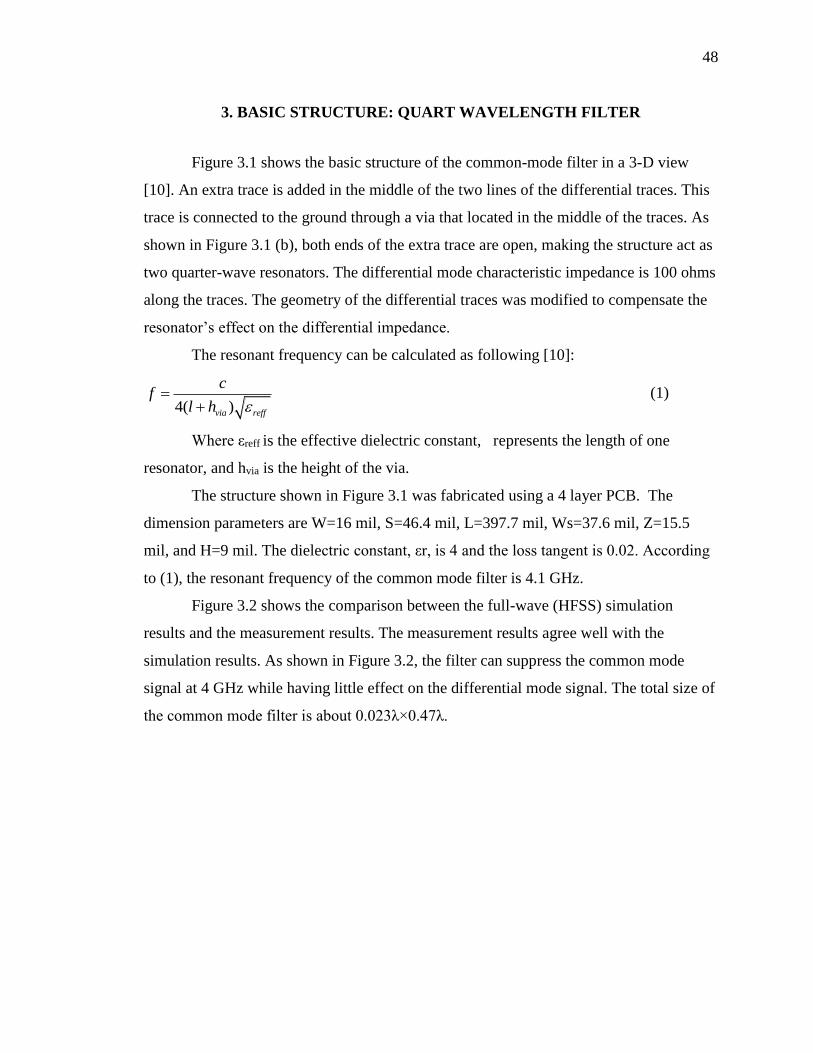
3. BASIC STRUCTURE: QUART WAVELENGTH FILTER
Figure 3.1 shows the basic structure of the common-mode filter in a 3-D view
[10]. An extra trace is added in the middle of the two lines of the differential traces. This
trace is connected to the ground through a via that located in the middle of the traces. As
shown in Figure 3.1 (b), both ends of the extra trace are open, making the structure act as
two quarter-wave resonators. The differential mode characteristic impedance is 100 ohms
along the traces. The geometry of the differential traces was modified to compensate the
resonator’s effect on the differential impedance.
The resonant frequency can be calculated as following [10]:
4( )via reff
cf
l h
(1)
Where εreff is the effective dielectric constant, represents the length of one
resonator, and hvia is the height of the via.
The structure shown in Figure 3.1 was fabricated using a 4 layer PCB. The
dimension parameters are W=16 mil, S=46.4 mil, L=397.7 mil, Ws=37.6 mil, Z=15.5
mil, and H=9 mil. The dielectric constant, εr, is 4 and the loss tangent is 0.02. According
to (1), the resonant frequency of the common mode filter is 4.1 GHz.
Figure 3.2 shows the comparison between the full-wave (HFSS) simulation
results and the measurement results. The measurement results agree well with the
simulation results. As shown in Figure 3.2, the filter can suppress the common mode
signal at 4 GHz while having little effect on the differential mode signal. The total size of
the common mode filter is about 0.023λ×0.47λ.
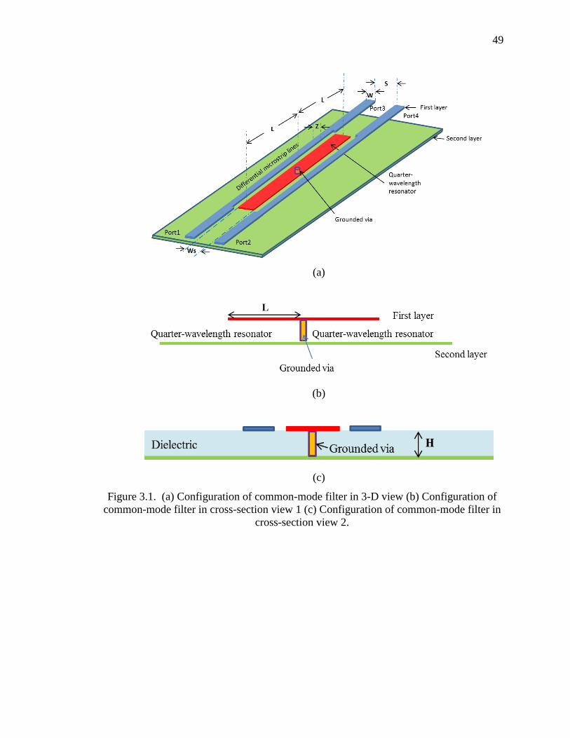
49
(a)
(b)
(c)
Figure 3.1. (a) Configuration of common-mode filter in 3-D view (b) Configuration of
common-mode filter in cross-section view 1 (c) Configuration of common-mode filter in
cross-section view 2.

50
0 1 2 3 4 5 6 7 8-16
-14
-12
-10
-8
-6
-4
-2
0
2
Frequency, GHz
Magnitude (
dB
)
Scc21-Measure
Sdd21-Measure
Sdd21-HFSS
Scc21-HFSS
Figure 3.2. Comparisons of the simulation results of S-parameters between full-wave
simulation and test PCB board measurement for Figure 3.1.
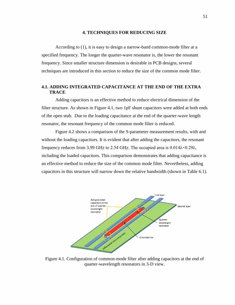
51
4. TECHNIQUES FOR REDUCING SIZE
According to (1), it is easy to design a narrow-band common-mode filter at a
specified frequency. The longer the quarter-wave resonator is, the lower the resonant
frequency. Since smaller structure dimension is desirable in PCB designs, several
techniques are introduced in this section to reduce the size of the common mode filter.
4.1. ADDING INTEGRATED CAPACITANCE AT THE END OF THE EXTRA
TRACE
Adding capacitors is an effective method to reduce electrical dimension of the
filter structure. As shown in Figure 4.1, two 1pF shunt capacitors were added at both ends
of the open stub. Due to the loading capacitance at the end of the quarter-wave length
resonator, the resonant frequency of the common mode filter is reduced.
Figure 4.2 shows a comparison of the S-parameter measurement results, with and
without the loading capacitors. It is evident that after adding the capacitors, the resonant
frequency reduces from 3.99 GHz to 2.54 GHz. The occupied area is 0.014λ×0.29λ,
including the loaded capacitors. This comparison demonstrates that adding capacitance is
an effective method to reduce the size of the common mode filter. Nevertheless, adding
capacitors in this structure will narrow down the relative bandwidth (shown in Table 6.1).
Figure 4.1. Configuration of common-mode filter after adding capacitors at the end of
quarter-wavelength resonators in 3-D view.

52
Figure 4.2. Comparison of measured response for normal quarter wavelength resonator
structure to the same structure with added 1 pF capacitors.
4.2. RESONATOR UNDERNEATH THE DIFFERENTIAL TRACE
In this variant case, as shown in Figure 4.3, the quarter-wave resonator is placed
on the second layer. The third layer is ground plane. The undisturbed second layer
ground, which surrounds the resonator, connects the third layer ground by via walls as
shown in Figure 4.3 (b). This structure uses one more layer, locally. By doing this, it
achieves stronger coupling to the differential trace. The dimensions are W=200 mil,
L1=393.7 mil, H1= 40 mil, and H2 = 49 mil. The effective dielectric constant is 4.2. The
width of the gap around the resonator is 6 mil. The capacitances at the gaps and to the
third layer help to reduce the resonant frequency.
Figure 4.4 shows the simulation results for the common mode filter presented in
Figure 4.3. The resonant frequency is 3.1 GHz. In this case, the corresponding electrical
size is 0.1λ×0.2λ. Although the occupied area is larger than the structure shown in Figure
3.1 and Figure 4.1, the bandwidth for this structure is much wider.

53
(a)
(b)
Figure 4.3. (a) Configuration of the common-mode filter in 3-D view (b) Configuration
of the common-mode filter in cross-sectional view.
Figure 4.5 (a) shows a modified geometry of the resonator, which increases the
inductance to reduce the electrical size of the resonators. Figure 4.5 (b) shows another
structure (modified from Figure 3.1 (b)), in which additional traces are added underneath
the ground plane using vias. The resonant frequency is reduced by this extra structure.
One can view these extensions in the third layer as short transmission lines or as loading
capacitors. Both models lead to decreased resonant frequency. This reduces the area of
the resonant filter, by occupying another layer.

54
0.00 1.00 2.00 3.00 4.00 5.00 6.00 7.00 8.00Freq [GHz]
-22.50
-20.00
-17.50
-15.00
-12.50
-10.00
-7.50
-5.00
-2.50
0.00
Y1
Discontinuted gap in second layerSimulation result
m1
Curve Info
dB(St(Diff1,Diff2))Setup1 : Sw eep
dB(St(Comm1,Comm2))Setup1 : Sw eep
Name X Y
m1 3.1000 -21.8213
Figure 4.4. Full wave simulated S-parameters for the structure shown in Figure 4.3.
(a) (b)
Figure 4.5. (a) Inductive loaded for resonator and (b) Cross-section for added traces
underneath ground plane for reduced resonance frequency.

55
5. PROPOSED NOVEL STRUCTURE
Based on the techniques discussed above, a new common mode filter structure is
proposed, as shown in Figure 5.1. Two resonators are implemented in this structure. The
first resonator is placed on the top layer and the second resonator is placed on the second
layer. An inter-digital structure is used in the second layer. The ground on the second
layer and third layer are connected through a wall of vias. The dimensions are W1=15.5
mil, W2=26 mil, H1=49 mil, H2=40 mil, L1=401.2 mil,L2=370 mil, W3=240 mil, and
W4=96 mil.
(a)
Figure 5.1. (a) Configuration of the new CMF in 3-D view (b) Cross-sectional view (c)
Top view for the second layer and (d) Top view of second layer.
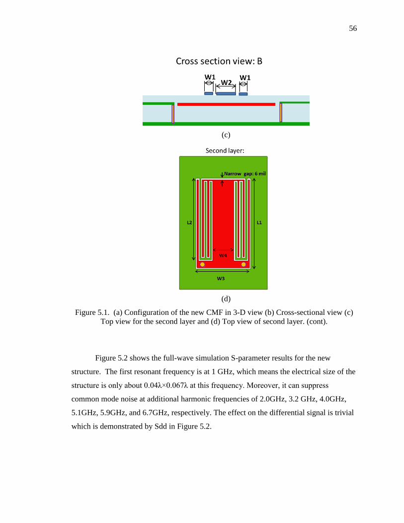
56
(c)
(d)
Figure 5.1. (a) Configuration of the new CMF in 3-D view (b) Cross-sectional view (c)
Top view for the second layer and (d) Top view of second layer. (cont).
Figure 5.2 shows the full-wave simulation S-parameter results for the new
structure. The first resonant frequency is at 1 GHz, which means the electrical size of the
structure is only about 0.04λ×0.067λ at this frequency. Moreover, it can suppress
common mode noise at additional harmonic frequencies of 2.0GHz, 3.2 GHz, 4.0GHz,
5.1GHz, 5.9GHz, and 6.7GHz, respectively. The effect on the differential signal is trivial
which is demonstrated by Sdd in Figure 5.2.

57
Figure 5.2. Simulation results of the S-parameters from full-wave simulation for the
structure shown in Figure 5.1
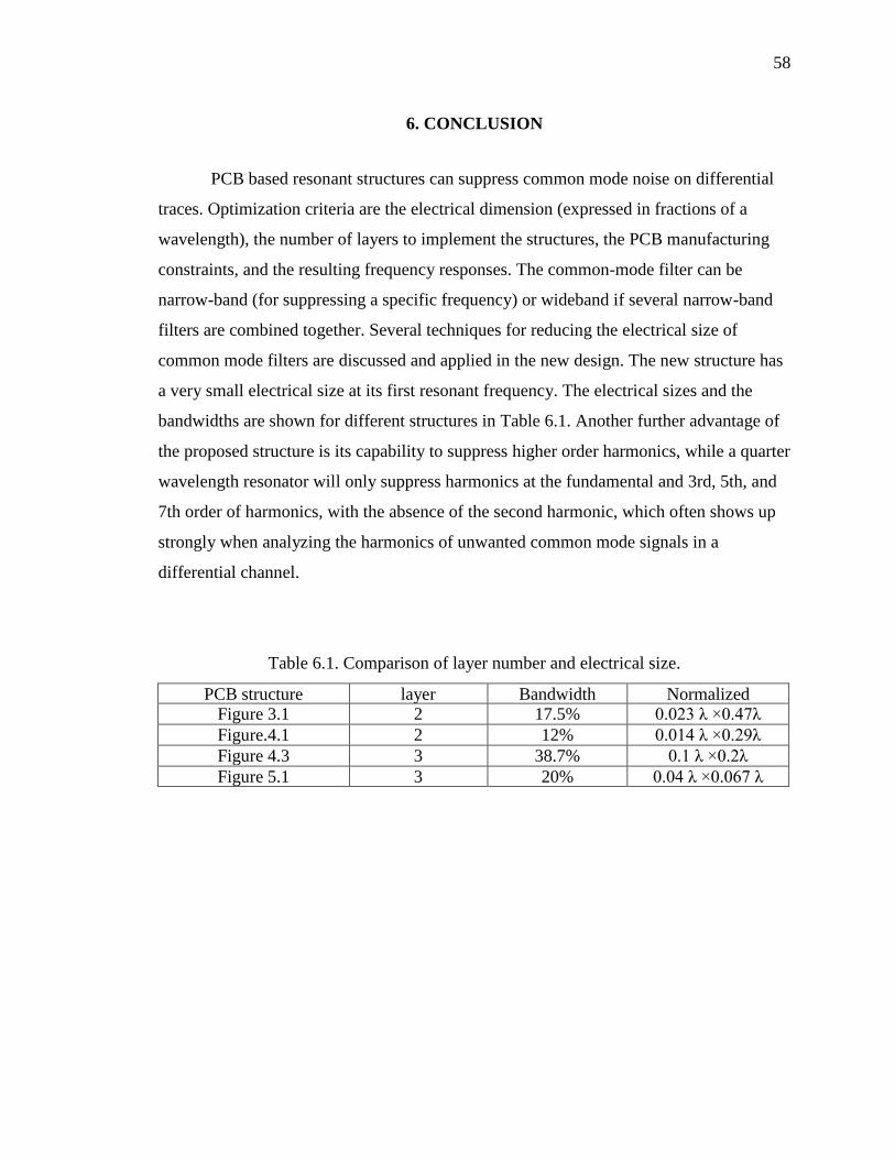
58
6. CONCLUSION
PCB based resonant structures can suppress common mode noise on differential
traces. Optimization criteria are the electrical dimension (expressed in fractions of a
wavelength), the number of layers to implement the structures, the PCB manufacturing
constraints, and the resulting frequency responses. The common-mode filter can be
narrow-band (for suppressing a specific frequency) or wideband if several narrow-band
filters are combined together. Several techniques for reducing the electrical size of
common mode filters are discussed and applied in the new design. The new structure has
a very small electrical size at its first resonant frequency. The electrical sizes and the
bandwidths are shown for different structures in Table 6.1. Another further advantage of
the proposed structure is its capability to suppress higher order harmonics, while a quarter
wavelength resonator will only suppress harmonics at the fundamental and 3rd, 5th, and
7th order of harmonics, with the absence of the second harmonic, which often shows up
strongly when analyzing the harmonics of unwanted common mode signals in a
differential channel.
Table 6.1. Comparison of layer number and electrical size.
PCB structure layer Bandwidth Normalized Figure 3.1 2 17.5% 0.023 λ ×0.47λ
Figure.4.1 2 12% 0.014 λ ×0.29λ
Figure 4.3 3 38.7% 0.1 λ ×0.2λ
Figure 5.1 3 20% 0.04 λ ×0.067 λ
59
REFERENCES
[1] C. Chang, R. Fang, C. Wang, “Bended Differential transmission line using
compensation inductance for common-mode noise suppression”, IEEE Trans. Comp.,
Packag. Manf. Technol. vol. 2, pp. 1518-1525, Sep. 2012.
[2] C. Chang, R. Fang, C. Wang, “Bended Differential transmission line using
compensation inductance for common-mode noise suppression”, IEEE Trans. Comp.,
Packag. Manf. Technol. vol. 2, pp. 1518-1525, Sep. 2012.
[3] Chung-Hao Tsai; Jing-Zuei Hsu; Iat-In Ao Ieong; Tzong-Lin Wu, "A novel common
mode choke and its application for 5 Gbps USB 3.0," Electromagnetic Compatibility
(EMC), 2011 IEEE International Symposium on , vol., no., pp.888,891, 14-19 Aug.
2011.
[4] Wei-Tzong Liu; Chung-Hao Tsai; Tzu-Wei Han; Tzong-Lin Wu, "An Embedded
Common-Mode Suppression Filter for GHz Differential Signals Using Periodic
Defected Ground Plane," Microwave and Wireless Components Letters, IEEE ,
vol.18, no.4, pp.248,250, April 2008.
[5] Chih-Ying Hsiao; Chung-Hao Tsai; Cheng-Nan Chiu; Tzong-Lin Wu, "Radiation
Suppression for Cable-Attached Packages Utilizing a Compact Embedded Common-
Mode Filter," Components, Packaging and Manufacturing Technology, IEEE
Transactions on , vol.2, no.10, pp.1696,1703, Oct. 2012.
[6] Hao-Hsiang Chuang; Tzong-Lin Wu, "A Novel Ground Resonator Technique to
Reduce Common-Mode Radiation on Slot-Crossing Differential Signals," Microwave
and Wireless Components Letters, IEEE , vol.20, no.12, pp.660,662, Dec. 2010.
[7] Jui-Chih Yen; Sen-Kuei Hsu; Tong-Hong Lin; Tzong-Lin Wu, "A Broadband
Forward-Wave Directional Coupler Using Periodic Y-Shaped Ground Via Structures
With Arbitrary Coupling Levels," Microwave Theory and Techniques, IEEE
Transactions on, vol.61, no.1, pp.38,47, Jan. 2013.
[8] Wu, T.-L.; Chung-Hao Tsai; Tzong-Lin Wu; Itoh, T., "A Novel Wideband Common-
Mode Suppression Filter for Gigahertz Differential Signals Using Coupled Patterned
Ground Structure," Microwave Theory and Techniques, IEEE Transactions on ,
vol.57, no.4, pp.848,855, April 2009.
[9] de Paulis, F.; Raimondo, L.; Connor, S.; Archambeault, B.; Orlandi, A., "Compact
Configuration for Common Mode Filter Design based on Planar Electromagnetic
Bandgap Structures," Electromagnetic Compatibility, IEEE Transactions on , vol.54,
no.3, pp.646,654, June 2012.
60
[10] Shiue, G.-H.; Hsu, C.-M.; Yeh, C.-L.; Hsu, C.-F., "A Comprehensive Investigation
of a Common-Mode Filter for Gigahertz Differential Signals Using Quarter-
Wavelength Resonators," Components, Packaging and Manufacturing Technology,
IEEE Transactions on , vol.4, no.1, pp.134,144, Jan. 2013.
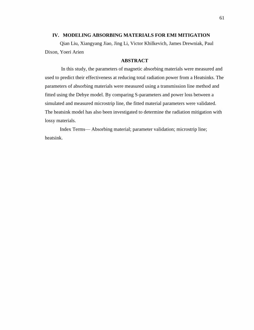
61
IV. MODELING ABSORBING MATERIALS FOR EMI MITIGATION
Qian Liu, Xiangyang Jiao, Jing Li, Victor Khilkevich, James Drewniak, Paul
Dixon, Yoeri Arien
ABSTRACT
In this study, the parameters of magnetic absorbing materials were measured and
used to predict their effectiveness at reducing total radiation power from a Heatsinks. The
parameters of absorbing materials were measured using a transmission line method and
fitted using the Debye model. By comparing S-parameters and power loss between a
simulated and measured microstrip line, the fitted material parameters were validated.
The heatsink model has also been investigated to determine the radiation mitigation with
lossy materials.
Index Terms— Absorbing material; parameter validation; microstrip line;
heatsink.
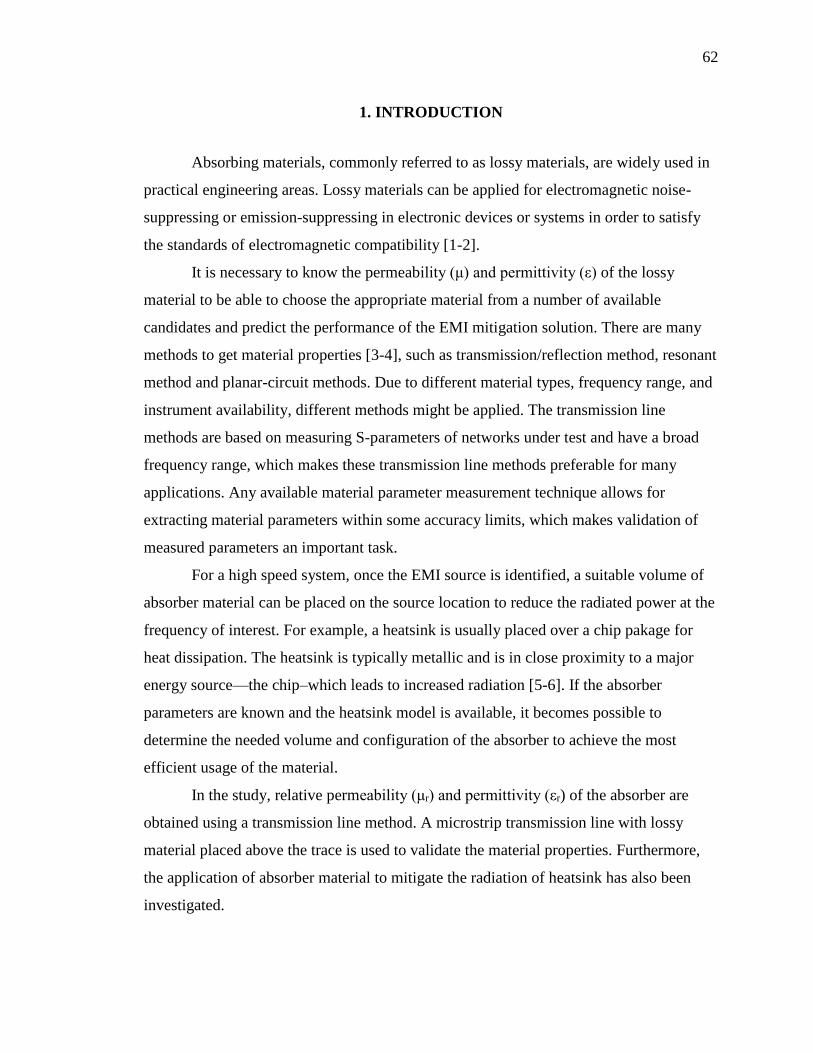
62
1. INTRODUCTION
Absorbing materials, commonly referred to as lossy materials, are widely used in
practical engineering areas. Lossy materials can be applied for electromagnetic noise-
suppressing or emission-suppressing in electronic devices or systems in order to satisfy
the standards of electromagnetic compatibility [1-2].
It is necessary to know the permeability (μ) and permittivity (ε) of the lossy
material to be able to choose the appropriate material from a number of available
candidates and predict the performance of the EMI mitigation solution. There are many
methods to get material properties [3-4], such as transmission/reflection method, resonant
method and planar-circuit methods. Due to different material types, frequency range, and
instrument availability, different methods might be applied. The transmission line
methods are based on measuring S-parameters of networks under test and have a broad
frequency range, which makes these transmission line methods preferable for many
applications. Any available material parameter measurement technique allows for
extracting material parameters within some accuracy limits, which makes validation of
measured parameters an important task.
For a high speed system, once the EMI source is identified, a suitable volume of
absorber material can be placed on the source location to reduce the radiated power at the
frequency of interest. For example, a heatsink is usually placed over a chip pakage for
heat dissipation. The heatsink is typically metallic and is in close proximity to a major
energy source—the chip–which leads to increased radiation [5-6]. If the absorber
parameters are known and the heatsink model is available, it becomes possible to
determine the needed volume and configuration of the absorber to achieve the most
efficient usage of the material.
In the study, relative permeability (μr) and permittivity (εr) of the absorber are
obtained using a transmission line method. A microstrip transmission line with lossy
material placed above the trace is used to validate the material properties. Furthermore,
the application of absorber material to mitigate the radiation of heatsink has also been
investigated.
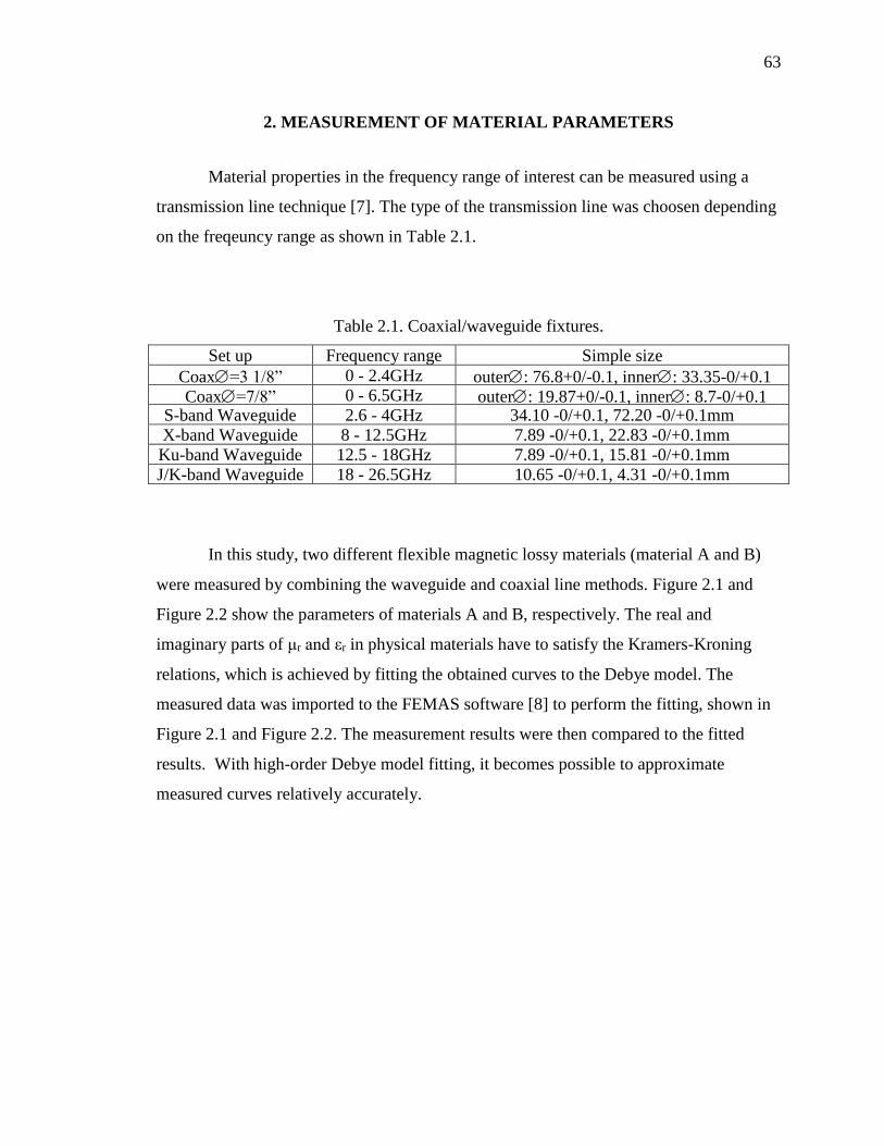
63
2. MEASUREMENT OF MATERIAL PARAMETERS
Material properties in the frequency range of interest can be measured using a
transmission line technique [7]. The type of the transmission line was choosen depending
on the freqeuncy range as shown in Table 2.1.
Table 2.1. Coaxial/waveguide fixtures.
Set up Frequency range Simple size
Coax=3 1/8” 0 - 2.4GHz outer: 76.8+0/-0.1, inner: 33.35-0/+0.1
Coax=7/8” 0 - 6.5GHz outer: 19.87+0/-0.1, inner: 8.7-0/+0.1 S-band Waveguide 2.6 - 4GHz 34.10 -0/+0.1, 72.20 -0/+0.1mm
X-band Waveguide 8 - 12.5GHz 7.89 -0/+0.1, 22.83 -0/+0.1mm
Ku-band Waveguide 12.5 - 18GHz 7.89 -0/+0.1, 15.81 -0/+0.1mm
J/K-band Waveguide 18 - 26.5GHz 10.65 -0/+0.1, 4.31 -0/+0.1mm
In this study, two different flexible magnetic lossy materials (material A and B)
were measured by combining the waveguide and coaxial line methods. Figure 2.1 and
Figure 2.2 show the parameters of materials A and B, respectively. The real and
imaginary parts of μr and εr in physical materials have to satisfy the Kramers-Kroning
relations, which is achieved by fitting the obtained curves to the Debye model. The
measured data was imported to the FEMAS software [8] to perform the fitting, shown in
Figure 2.1 and Figure 2.2. The measurement results were then compared to the fitted
results. With high-order Debye model fitting, it becomes possible to approximate
measured curves relatively accurately.
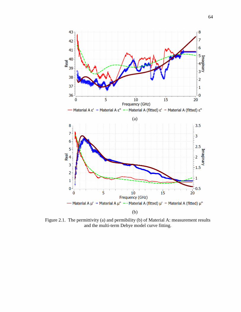
64
(a)
(b)
Figure 2.1. The permittivity (a) and permibility (b) of Material A: measurement results
and the multi-term Debye model curve fitting.

65
(a)
(b)
Figure 2.2. The permittivity (a) and permeability (b) of material B: measurement results
and the multi-term Debye model curve fitting
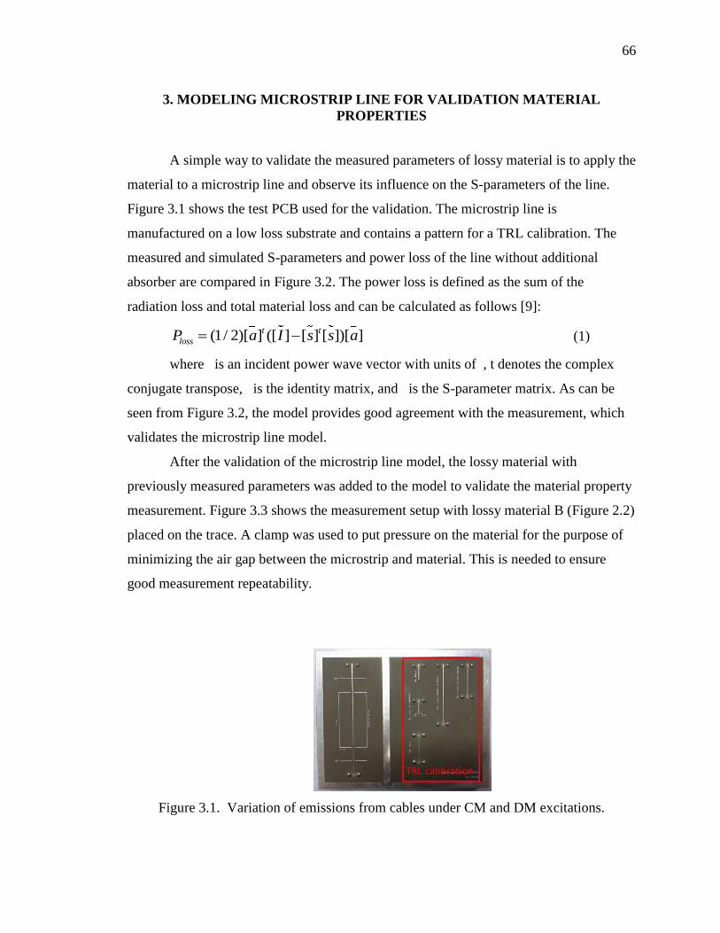
66
3. MODELING MICROSTRIP LINE FOR VALIDATION MATERIAL
PROPERTIES
A simple way to validate the measured parameters of lossy material is to apply the
material to a microstrip line and observe its influence on the S-parameters of the line.
Figure 3.1 shows the test PCB used for the validation. The microstrip line is
manufactured on a low loss substrate and contains a pattern for a TRL calibration. The
measured and simulated S-parameters and power loss of the line without additional
absorber are compared in Figure 3.2. The power loss is defined as the sum of the
radiation loss and total material loss and can be calculated as follows [9]:
(1/ 2)[ ] ([ ] [ ] [ ])[ ]t t
lossP a I s s a (1)
where is an incident power wave vector with units of , t denotes the complex
conjugate transpose, is the identity matrix, and is the S-parameter matrix. As can be
seen from Figure 3.2, the model provides good agreement with the measurement, which
validates the microstrip line model.
After the validation of the microstrip line model, the lossy material with
previously measured parameters was added to the model to validate the material property
measurement. Figure 3.3 shows the measurement setup with lossy material B (Figure 2.2)
placed on the trace. A clamp was used to put pressure on the material for the purpose of
minimizing the air gap between the microstrip and material. This is needed to ensure
good measurement repeatability.
Figure 3.1. Variation of emissions from cables under CM and DM excitations.
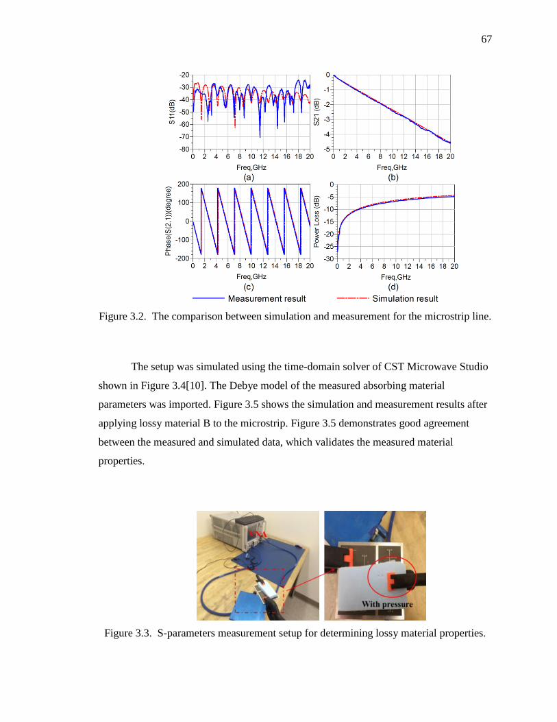
67
Figure 3.2. The comparison between simulation and measurement for the microstrip line.
The setup was simulated using the time-domain solver of CST Microwave Studio
shown in Figure 3.4[10]. The Debye model of the measured absorbing material
parameters was imported. Figure 3.5 shows the simulation and measurement results after
applying lossy material B to the microstrip. Figure 3.5 demonstrates good agreement
between the measured and simulated data, which validates the measured material
properties.
Figure 3.3. S-parameters measurement setup for determining lossy material properties.
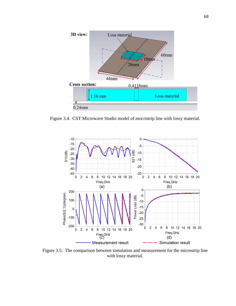
68
Figure 3.4. CST Microwave Studio model of mocristrip line with lossy material.
Figure 3.5. The comparison between simulation and measurement for the microstrip line
with lossy material.
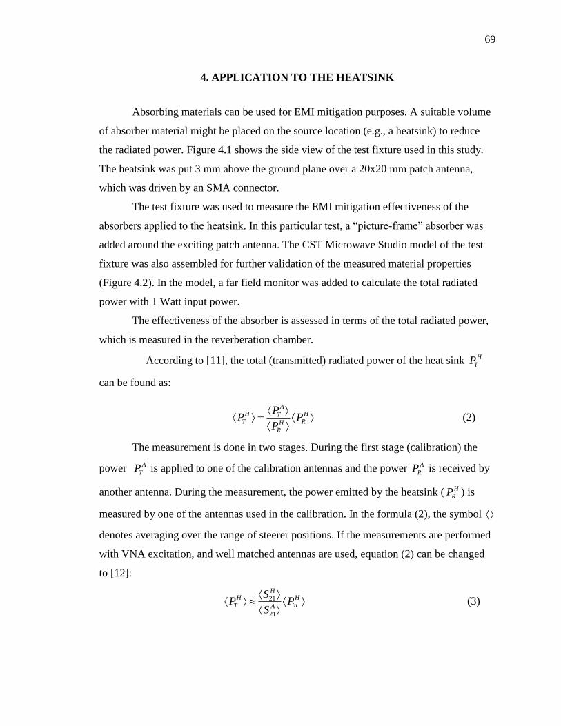
69
4. APPLICATION TO THE HEATSINK
Absorbing materials can be used for EMI mitigation purposes. A suitable volume
of absorber material might be placed on the source location (e.g., a heatsink) to reduce
the radiated power. Figure 4.1 shows the side view of the test fixture used in this study.
The heatsink was put 3 mm above the ground plane over a 20x20 mm patch antenna,
which was driven by an SMA connector.
The test fixture was used to measure the EMI mitigation effectiveness of the
absorbers applied to the heatsink. In this particular test, a “picture-frame” absorber was
added around the exciting patch antenna. The CST Microwave Studio model of the test
fixture was also assembled for further validation of the measured material properties
(Figure 4.2). In the model, a far field monitor was added to calculate the total radiated
power with 1 Watt input power.
The effectiveness of the absorber is assessed in terms of the total radiated power,
which is measured in the reverberation chamber.
According to [11], the total (transmitted) radiated power of the heat sink H
TP
can be found as:
A
H HTT RH
R
PP P
P
(2)
The measurement is done in two stages. During the first stage (calibration) the
power A
TP is applied to one of the calibration antennas and the power A
RP is received by
another antenna. During the measurement, the power emitted by the heatsink ( H
RP ) is
measured by one of the antennas used in the calibration. In the formula (2), the symbol
denotes averaging over the range of steerer positions. If the measurements are performed
with VNA excitation, and well matched antennas are used, equation (2) can be changed
to [12]:
21
21
HH H
T inA
SP P
S
(3)

70
Where 21
AS is the transmission coefficient between two calibration antennas
(shown in Figure 4.3) and 21
HS is the transmission coefficient between the heat sink and
one of the antennas (shown in Figure 4.4), and H
inP is the assumed power applied to the
heatsink.
Figure 4.1. Side view of measured heatsink with square metal patch as the excitation.
(a) (b)
(c) (d)
Figure 4.2. CST Microwave Studio model: (a) patch between the ground and heatsink (b)
cross section view of the model (c) a picture frame absober is added to the bottem of the
heatsink (d) picture frame lossy material
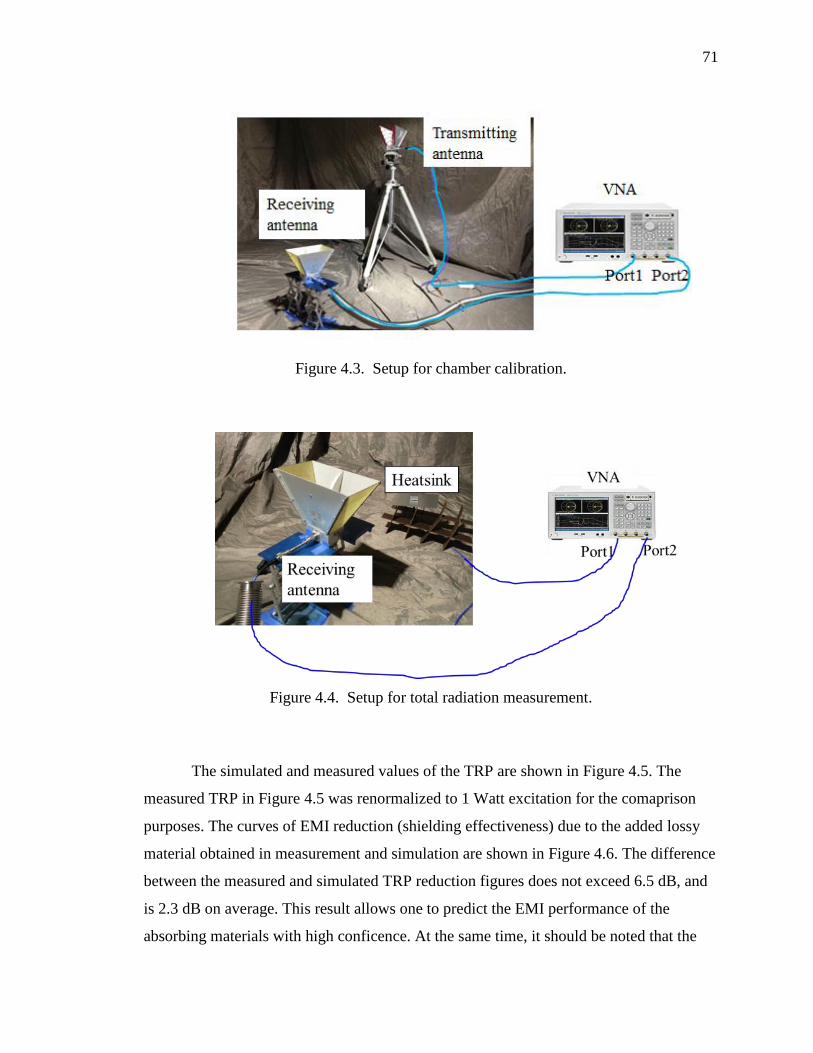
71
Figure 4.3. Setup for chamber calibration.
Figure 4.4. Setup for total radiation measurement.
The simulated and measured values of the TRP are shown in Figure 4.5. The
measured TRP in Figure 4.5 was renormalized to 1 Watt excitation for the comaprison
purposes. The curves of EMI reduction (shielding effectiveness) due to the added lossy
material obtained in measurement and simulation are shown in Figure 4.6. The difference
between the measured and simulated TRP reduction figures does not exceed 6.5 dB, and
is 2.3 dB on average. This result allows one to predict the EMI performance of the
absorbing materials with high conficence. At the same time, it should be noted that the
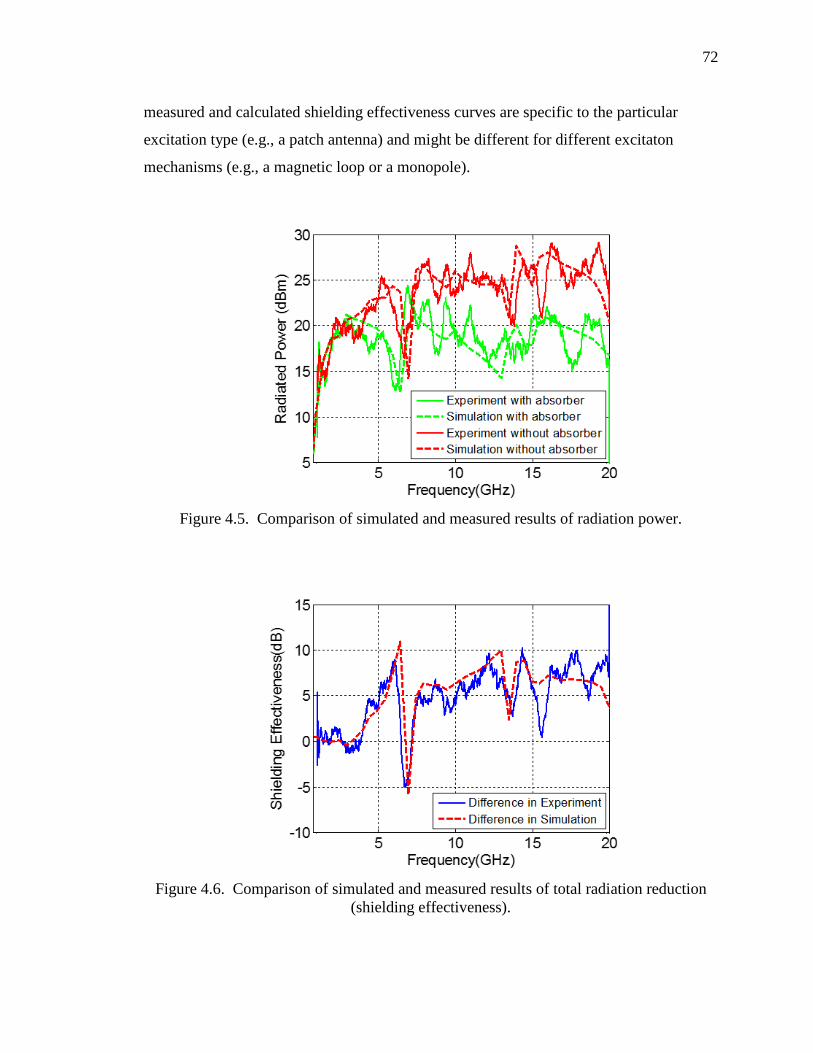
72
measured and calculated shielding effectiveness curves are specific to the particular
excitation type (e.g., a patch antenna) and might be different for different excitaton
mechanisms (e.g., a magnetic loop or a monopole).
Figure 4.5. Comparison of simulated and measured results of radiation power.
Figure 4.6. Comparison of simulated and measured results of total radiation reduction
(shielding effectiveness).
73
5. CONCLUSION
The transmission line measurement method allows measuring the material
parameters of flexible magnetic absorbers with relatively good accuracy. The
measurement was validated by the microstrip line measurement and in the heatsink test
fixture. The microstrip line test can be recommended as an easy-to-implement validation
method for the measured material parameters.
The whole measurement and simulation procedure allows predicting the EMI
mitigation performance of magnetic absorbers with an average accuracy of approximately
2 dB, which makes it accurate enough for practical EMC applications.
74
REFERENCES
[1] Jing Li; Koledintseva, M.Y.; Razmadze, A.; Gafarov, A.; Yao-Jiang Zhang;
Drewniak, J.L.; Jun Fan; Shenhui, J., "Permeability and permittivity uncertainty
effects in modeling absorbing coatings and ferrites on cables," Electromagnetic
Compatibility (EMC), 2012 IEEE International Symposium on , vol., no., pp.74,79,
6-10 Aug. 2012.
[2] J. Li, Y.-J. Zhang, A. Gafarov, S. De, M. Koledintseva, J. Marchand, D. Hess, T.
Durant, J. Drewniak, and J. Fan, “EMI reduction evaluation with flexible absorbing
materials and ferrite cores applied on cables”, Proc. IEEE Symp. Electromag.
Compat., Pittsburg, PA, Aug. 5-10, 2012.
[3] L.F. Chen, C.K. Ong, C.P. Neo, V.V. Varadan, and V.K. Varadan, Microwave
Electronics – Measurement and Material Characterisation, Wiley, 2004.
[4] Bush Space Company, Gary G., "Measurement techniques for permeability,
permittivity and EMI shielding: a review," Electromagnetic Compatibility, 1994.
Symposium Record. Compatibility in the Loop., IEEE International Symposium on ,
vol., no., pp.333,339, 22-26 Aug 1994.
[5] X. Zhou, Jing Li, H. Fan, A. Bhobe, K. Taunk, J. Yu, P. Sochoux, “Validating EMC
Simulation by Measurement in Reverberation Chamber,” Designcon 2013, San Jose,
CA, January 28-31, 2013.
[6] X. Zhou, Jing. Li, H. Fan, A. Bhobe, P. Sochoux, J. Yu, "High-frequency EMC
design verification through full-wave simulations and measurements in Reverberation
Chamber,” in proceedings of IEEE International Symposium on Electromagnetic
Compatibility, Denver, CO, Aug. 2013, pp. 299-305.
[7] Baker-Jarvis and etal, "Measuring the permittivity and permeability of lossy
materials: solid, liquids, metals, building materials and negative -index materials,"
NIST technical note 1536, Feb. 2005.
[8] http://www.ems-plus.com/FEMAS_main.html.
[9] X. Tian, M. S. Halligan, X. Li, K. Kim, H.-C. Chen, S. Connor, B. Archambeault, M.
Cracraft, A. E. Ruehli, and J. L. Drewniak, “Modeling electromagnetic radiation at
high-density PCB/connector interfaces,” presented at the IEEE Int. Symp.
Electromagn. Compat., Raleigh, NC, USA, Aug. 2014.
[10] CST MICROWAVE STUDIO. ver. 13, CST Computer Simulation Technology,
Available: https://www.cst.com/.
75
[11] G. Koepke and J. Ladbury, “Radiated Power Measurements in Reverberation
Chambers,” 56th ARFTG Conference Digest-Fall, vol.38, pp.1-7, 2000.
[12] Holloway, C.L.; Hill, D.A.; Sandroni, M.; Ladbury, J.M.; Coder, J.; Koepke, G.;
Marvin, A.C.; Yuhui He, "Use of Reverberation Chambers to Determine the
Shielding Effectiveness of Physically Small, Electrically Large Enclosures and
Cavities," Electromagnetic Compatibility, IEEE Transactions on , vol.50, no.4,
pp.770,782, Nov. 2008.

76
SECTION
2. CONCLUSIONS
Paper I, Paper II and Paper III show three common mode filters. The advantages
of the filter are numerous. PCB embedded filter can be put into PCB and easy to
manufacture. Removable EBG filter can be installed, substituted and removed by the
typical soldering assembly process, which is easy to meet the filter needs of PCB
differential link designers at any stage of the design process.
Paper IV shows transmission line measurement method to validate the material
parameters of flexible magnetic absorbers with relatively good accuracy. The
measurement was validated by the microstrip line measurement and in the heatsink test
fixture. The microstrip line test can be recommended as an easy-to-implement validation
method for the measured material parameters.
77
VITA
Qian Liu was born in Guangxi Province, P. R. China, 1990. She received the B.S.
degree in electrical engineering from the University of Electronic Science and
Technology of China, Chengdu, China, in 2013. In 2013 fall, she started her Master in the
Electrical and Computer Engineering Department at Missouri University of Science and
Technology. She has also worked as a fall Co-op at IBM Systems Group during Jun.-
Dec. 2015. She received her Master degree in July 2016 from Missouri University of
Science and Technology.