automotive emi reduction techniques, applications and
TRANSCRIPT
Automotive EMIReduction Techniques,Applications and Solutions
Robert Loke – MGTS in Santa Clara
Robert Blattner – System / Apps in Santa Clara
1

EMI Techniques for Automotive Applications:
The world is hurtling towards Electric Vehicles and Autonomous Cars. Semiconductor content of cars is
expected to increase ~ 10x by 2025. In this presentation we show challenges in EMI for new increasing
demanding automotive systems like ADAS, cameras, instrument cluster and infotainment. Then we show
the EMI mitigation techniques like filtering, spread spectrum and E-field shielding and compared the results.
2
What you’ll learn: 1. In this training, you will learn about new automotive application trends
2. You will learn EMI noise sources and about near E-Field coupling
3. Introducing EMI mitigation techniques, like switch node shaping, spread
spectrum, E-Field shielding techniques.
4. EMI measurement that show how much all of these techniques will reduce
and help to pass CISPR 25 are presented.
Course details:• Type: PPT Presentation
• Duration: 1:30h / English
• Audience: FAE, Apps, System Apps
TI Products and Solutions:• 2.1MHz LM53601
• 2.1MHz LM53603
• 2.1MHz LM53635
• 400kHz LMS3655
TI training - summary
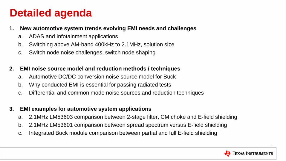
Detailed agenda
1. New automotive system trends evolving EMI needs and challenges
a. ADAS and Infotainment applications
b. Switching above AM-band 400kHz to 2.1MHz, solution size
c. Switch node noise challenges, switch node shaping
2. EMI noise source model and reduction methods / techniques
a. Automotive DC/DC conversion noise source model for Buck
b. Why conducted EMI is essential for passing radiated tests
c. Differential and common mode noise sources and reduction techniques
3. EMI examples for automotive system applications
a. 2.1MHz LM53603 comparison between 2-stage filter, CM choke and E-field shielding
b. 2.1MHz LM53601 comparison between spread spectrum versus E-field shielding
c. Integrated Buck module comparison between partial and full E-field shielding
3
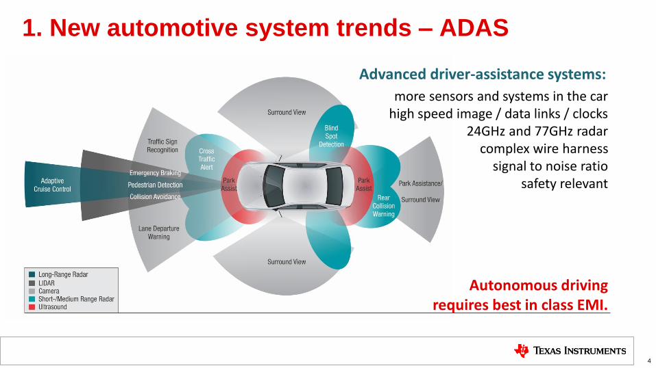
1. New automotive system trends – ADAS
4
more sensors and systems in the carhigh speed image / data links / clocks
24GHz and 77GHz radarcomplex wire harness
signal to noise ratiosafety relevant
Advanced driver-assistance systems:
Autonomous drivingrequires best in class EMI.
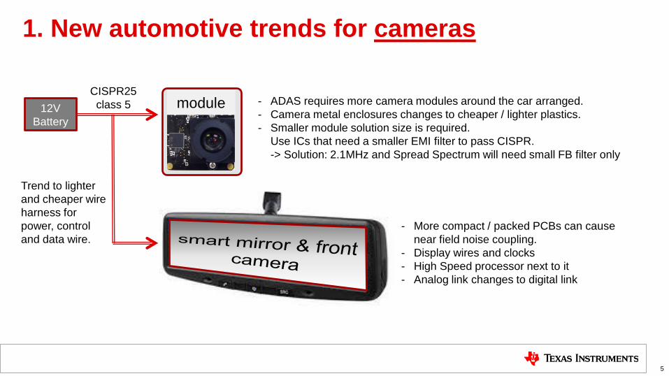
1. New automotive trends for cameras
5
12V
Battery
Trend to lighter
and cheaper wire
harness for
power, control
and data wire.
CISPR25
class 5 - ADAS requires more camera modules around the car arranged.
- Camera metal enclosures changes to cheaper / lighter plastics.
- Smaller module solution size is required.
Use ICs that need a smaller EMI filter to pass CISPR.
-> Solution: 2.1MHz and Spread Spectrum will need small FB filter only
- More compact / packed PCBs can cause
near field noise coupling.
- Display wires and clocks
- High Speed processor next to it
- Analog link changes to digital link
module
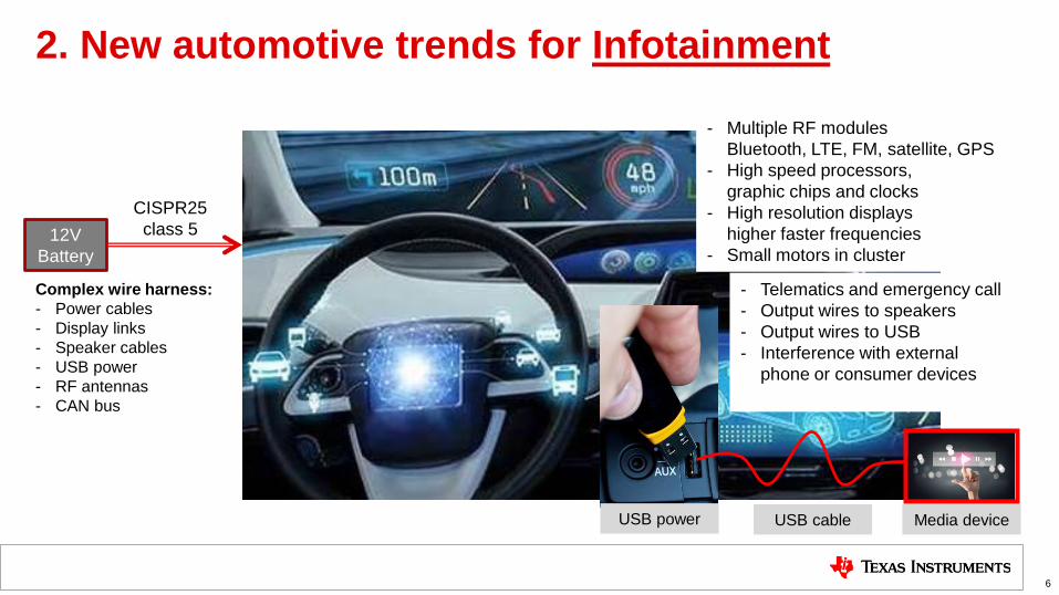
2. New automotive trends for Infotainment
6
12V
Battery
Complex wire harness:
- Power cables
- Display links
- Speaker cables
- USB power
- RF antennas
- CAN bus
- Telematics and emergency call
- Output wires to speakers
- Output wires to USB
- Interference with external
phone or consumer devices
- Multiple RF modules
Bluetooth, LTE, FM, satellite, GPS
- High speed processors,
graphic chips and clocks
- High resolution displays
higher faster frequencies
- Small motors in cluster
Media deviceUSB cableUSB power
CISPR25
class 5
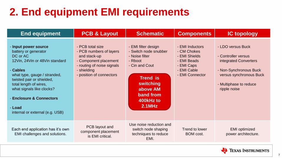
2. End equipment EMI requirements
7
End equipment PCB & Layout Schematic Components IC topology
- Input power source
battery or generator
DC or AC
12Vin, 24Vin or 48Vin standard
- Cables
what type, gauge / stranded,
twisted pair or shielded,
total length of wires,
what signals like clocks?
- Enclosure & Connectors
- Load
internal or external (e.g. USB)
- PCB total size
- PCB numbers of layers
and stack-up
- Component placement
- routing of noise signals
- shielding
- position of connectors
- EMI filter design
- Switch node snubber
- Noise filter
- Rboot
- Cin and Cout
- EMI Inductors
- CM Chokes
- EMI Shields
- EMI Beads
- EMI Caps
- EMI Cable
- EMI Connector
- LDO versus Buck
- Controller versus
integrated Converters
- Non-Synchronous Buck
versus synchronous Buck
- Multiphase to reduce
ripple noise
Each end application has it’s own
EMI challenges and solutions.
PCB layout and
component placement
is EMI critical.
Use noise reduction and
switch node shaping
techniques to reduce
EMI.
Trend to lower
BOM cost.
EMI optimized
power architecture.
Trend is
switching
above AM
band from
400kHz to
2.1MHz
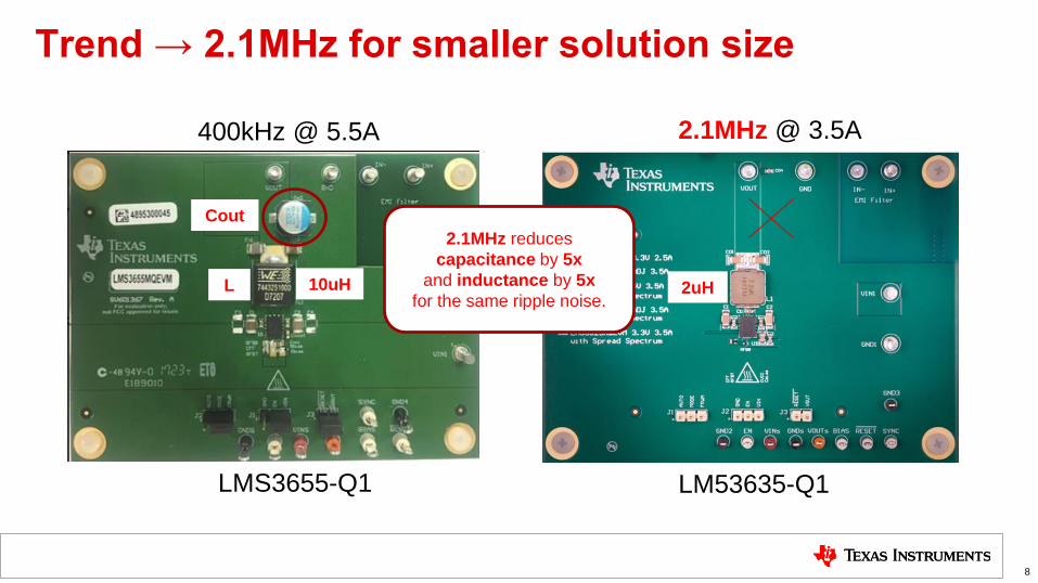
Trend → 2.1MHz for smaller solution size
8
2.1MHz @ 3.5A400kHz @ 5.5A
LM53635-Q1LMS3655-Q1
10uH 2uH
2.1MHz reduces
capacitance by 5x
and inductance by 5x
for the same ripple noise.
Cout
L
2.1MHz solution size advantage for low power
9
12mm 13mm
2.1MHz @ 2A
TSSOP package
LM53625-Q1LM53602-Q1LM53601-Q1
10mm
2.1MHz @ 1A
WSON package11uH
13x13
2.1MHz @ 2.5A
Hot Rod™ package
10
mm
Cout= 2x22uF
Cin = 1x10uF
Cout= 1x47uF
Cin = 1x10uF
Cout= 1x22uF
Cin = 1x10uF
10
mm4x4 4x4
10
mm
4x4

400kHz sinusoidal FFT
10
400kHz
Fundamental 1MHz 10MHz 100MHz
400kHz trapezoidal
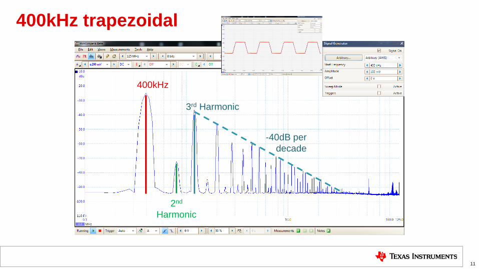
11
400kHz
2nd
Harmonic
3rd Harmonic
-40dB per
decade

-40dB per
decade
400kHz square
12
400kHz
-20dB per
decade
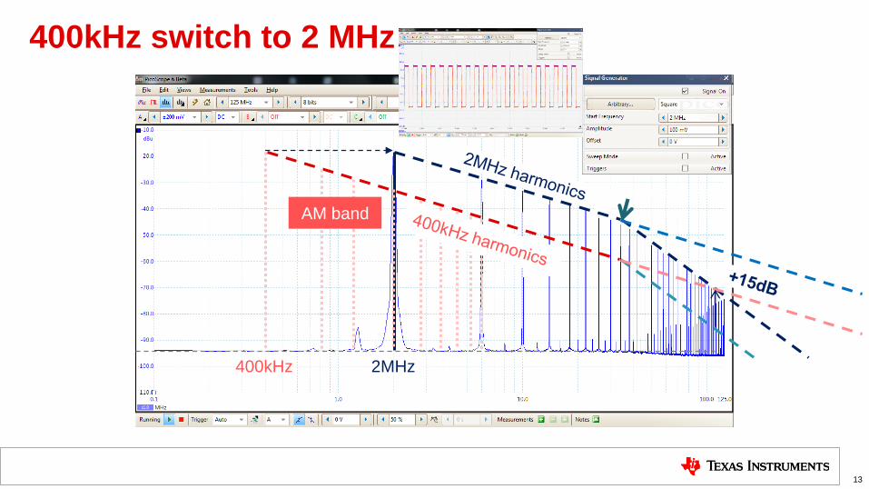
400kHz switch to 2 MHz
13
2MHz400kHz
AM band
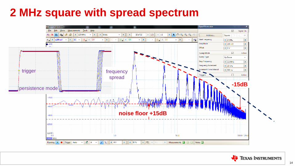
2 MHz square with spread spectrum
14
noise floor +15dB
-15dBpersistence mode
trigger frequency
spread
Car Metal Chassis
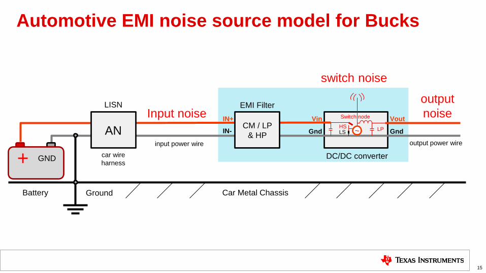
Automotive EMI noise source model for Bucks
15
Ground
input power wire
DC/DC converter
CM / LP
& HP
EMI Filter
AN
GND+
LISN
Battery
Vin
Gnd
Vout
Gnd
output power wire
IN+
IN-
car wire
harness
output
noiseInput noise Switch node
HSLS
LP~
switch noise
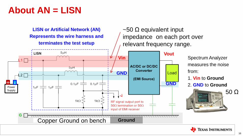
About AN = LISN
16
50 Ω
Spectrum Analyzer
measures the noise
from:
1. Vin to Ground
2. GND to Ground
LISN or Artificial Network (AN)
Represents the wire harness and
terminates the test setup
Vin
GND
Ground
Power
Supply
+
Copper Ground on bench
Vout
GND-
~50 Ω equivalent input
impedance on each port over
relevant frequency range.
50 Ω
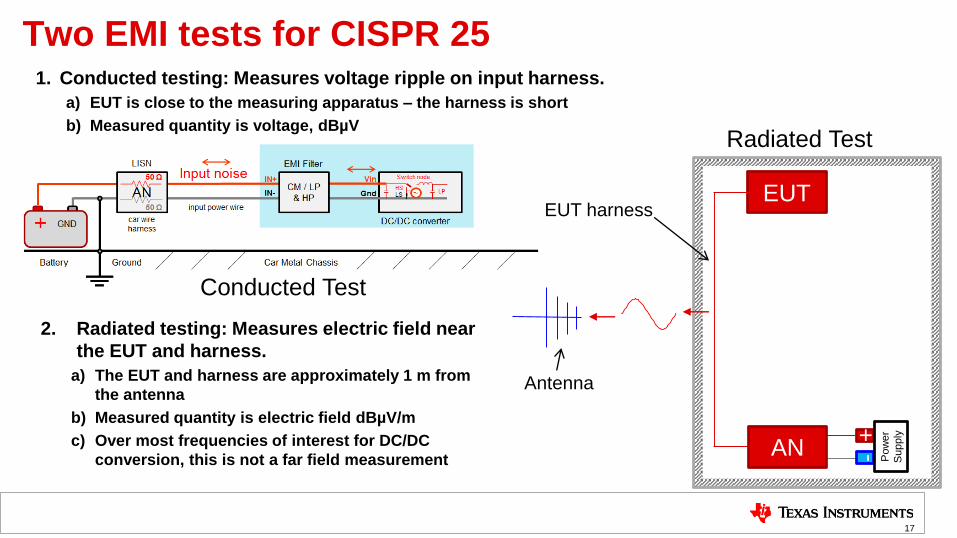
Two EMI tests for CISPR 25
17
1. Conducted testing: Measures voltage ripple on input harness.
a) EUT is close to the measuring apparatus – the harness is short
b) Measured quantity is voltage, dBµV
2. Radiated testing: Measures electric field near
the EUT and harness.
a) The EUT and harness are approximately 1 m from
the antenna
b) Measured quantity is electric field dBµV/m
c) Over most frequencies of interest for DC/DC
conversion, this is not a far field measurement
EUTEUT harness
Antenna
+
AN - Pow
er
Supply
Conducted Test
Radiated Test

About Conducted EMI
18
Power
SupplyAN EUT
Power
Supply
Side view
Top view
AN
AN EUT
Load
Simulator
Measuring
Instrument
Shielded enclosure 7 = Low relative permittivity support, eR < 1.4
8 = High-quality coaxial cable, e.g. double-shielded 50W
11 = 50W load
12 = Bulkhead connector
Ground plane
Power supply lines
EUT
AN
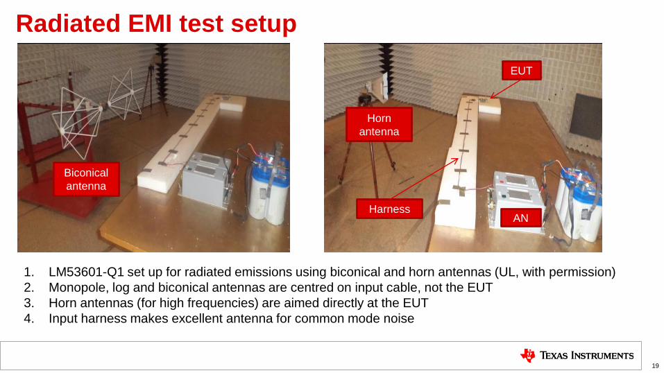
Radiated EMI test setup
19
1. LM53601-Q1 set up for radiated emissions using biconical and horn antennas (UL, with permission)
2. Monopole, log and biconical antennas are centred on input cable, not the EUT
3. Horn antennas (for high frequencies) are aimed directly at the EUT
4. Input harness makes excellent antenna for common mode noise
EUT
AN
Biconical
antenna
Harness
Horn
antenna
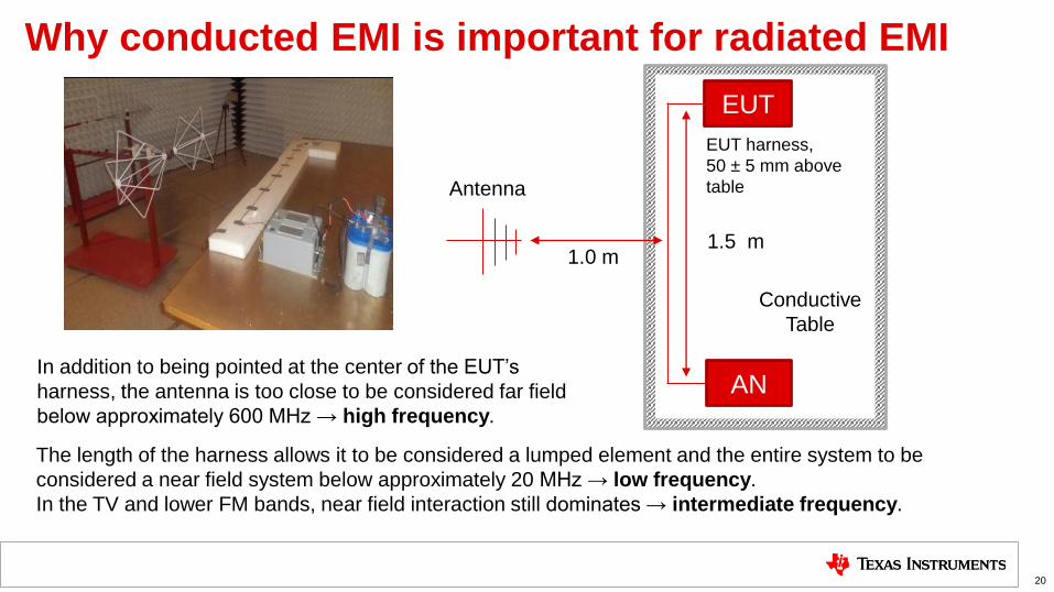
Why conducted EMI is important for radiated EMI
20
The length of the harness allows it to be considered a lumped element and the entire system to be
considered a near field system below approximately 20 MHz → low frequency.
In the TV and lower FM bands, near field interaction still dominates → intermediate frequency.
EUT
AN
1.0 m1.5 m
In addition to being pointed at the center of the EUT’s
harness, the antenna is too close to be considered far field
below approximately 600 MHz → high frequency.
Conductive
Table
EUT harness,
50 ± 5 mm above
tableAntenna
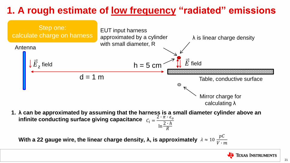
1. A rough estimate of low frequency “radiated” emissions
21
h = 5 cm
Table, conductive surface
Mirror charge for
calculating λ
Antenna
field𝐸zfield𝐸
λ is linear charge density
EUT input harness
approximated by a cylinder
with small diameter, R
1. λ can be approximated by assuming that the harness is a small diameter cylinder above an
infinite conducting surface giving capacitance
With a 22 gauge wire, the linear charge density, λ, is approximately
𝐶𝑙 =2 ∙ 𝜋 ∙ 𝜖𝑜
ln2 ∙ ℎ𝑅
d = 1 m
𝜆 ≈ 10𝑝𝐶
𝑉 ∙ 𝑚
Step one:
calculate charge on harness
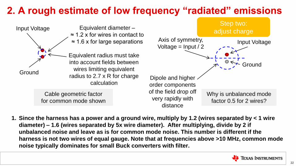
2. A rough estimate of low frequency “radiated” emissions
22
Why is unbalanced mode
factor 0.5 for 2 wires?
Input Voltage
Ground
Axis of symmetry,
Voltage = Input / 2
1. Since the harness has a power and a ground wire, multiply by 1.2 (wires separated by < 1 wire
diameter) – 1.6 (wires separated by 5x wire diameter). After multiplying, divide by 2 if
unbalanced noise and leave as is for common mode noise. This number is different if the
harness is not two wires of equal gauge. Note that at frequencies above >10 MHz, common mode
noise typically dominates for small Buck converters with filter.
Cable geometric factor
for common mode shown
Input Voltage
Ground
Equivalent diameter –
≈ 1.2 x for wires in contact to
≈ 1.6 x for large separations
Dipole and higher
order components
of the field drop off
very rapidly with
distance
Equivalent radius must take
into account fields between
wires limiting equivalent
radius to 2.7 x R for charge
calculation
Step two:
adjust charge

3. A rough estimate of low frequency “radiated” emissions
23
h = 5 cm
Conductive table
Antenna
field𝐸field𝐸
λ is linear
charge density
d = 1 m
1. Integrating the vertical component field produced by λ and ignoring its mirror charge and using
h = 5 cm, d = 1 m, harness length = 1.5 m closely spaced wires with common mode noise and
antenna vertically oriented electric field in V/m is ≈ 35 to 50 dB below conducted voltage in V.
2. mV level input ripple should be avoided since in most bands, radiated will fail as well as
conducted EMI testing
field𝐸
h = 0 for table so there
is no vertical field
component due to
induced charge
EUT
AN
d=1.0 m1.5 m
Antenna
field𝐸zsin(θ) = 0.6
Step three:
calculate electric field at antenna
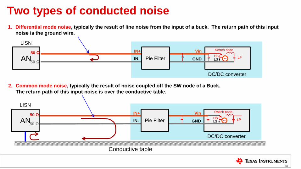
Two types of conducted noise
24
1. Differential mode noise, typically the result of line noise from the input of a buck. The return path of this input
noise is the ground wire.
DC/DC converter
AN
LISN
Vin
GND
IN+
IN-
Switch node
HSLS
LP~
50 Ω
50 ΩPie Filter
2. Common mode noise, typically the result of noise coupled off the SW node of a Buck.
The return path of this input noise is over the conductive table.
DC/DC converter
AN
LISN
Vin
GND
IN+
IN-
Switch node
HSLS
LP~
50 Ω
50 ΩPie Filter
Conductive table
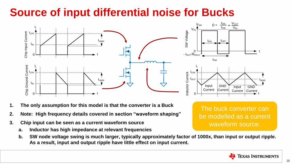
Source of input differential noise for Bucks
25
iL
VSW
ILPK
IOUT Iripple
Ind
ucto
r C
urr
en
t
- IOUT∙RDSLS
D =
t
t
0
0
SW
Vo
lta
ge
tON
tSWVIN
tSW
tON tOFF
VOUT
VIN≈
Input
Current
iL
ILPK
IIN
Iripple
Ch
ip In
pu
t C
urr
en
t
t0
GND
CurrentInput
Current
GND
Current
iL
ILPK
IIN
Iripple
Ch
ip G
rou
nd
Cu
rre
nt
t0
1. The only assumption for this model is that the converter is a Buck
2. Note: High frequency details covered in section “waveform shaping”
3. Chip input can be seen as a current waveform source
a. Inductor has high impedance at relevant frequencies
b. SW node voltage swing is much larger, typically approximately factor of 1000x, than input or output ripple.
As a result, input and output ripple have little effect on input current.
The buck converter can
be modelled as a current
waveform source.
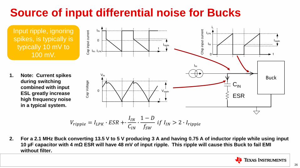
Source of input differential noise for Bucks
26
2. For a 2.1 MHz Buck converting 13.5 V to 5 V producing 3 A and having 0.75 A of inductor ripple while using input
10 µF capacitor with 4 mΩ ESR will have 48 mV of input ripple. This ripple will cause this Buck to fail EMI
without filter.
Input ripple, ignoring
spikes, is typically is
typically 10 mV to
100 mV.
1. Note: Current spikes
during switching
combined with input
ESL greatly increase
high frequency noise
in a typical system.
iL
ILPK
IIN
Iripple
Ch
ip in
pu
t cu
rre
nt
t0
Buck
IIN
IIN - ILPK
IIN
Iripple
Ca
p in
pu
t cu
rre
nt
t
0
VIN
Ca
p V
olta
ge
t
0 Vripple
𝑉𝑟𝑖𝑝𝑝𝑙𝑒 = 𝐼𝐿𝑃𝐾 ∙ 𝐸𝑆𝑅 +∙𝐼𝐼𝑁𝐶𝐼𝑁
∙1 − 𝐷
𝑓𝑆𝑊𝑖𝑓 𝐼𝐼𝑁 > 2 ∙ 𝐼𝑟𝑖𝑝𝑝𝑙𝑒
CIN
ESR
Conductive Table
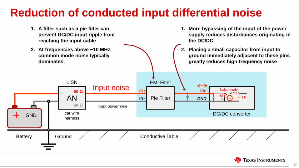
Reduction of conducted input differential noise
27
Ground
input power wire
DC/DC converter
Pie Filter
EMI Filter
AN
GND+
LISN
Battery
Vin
GND
IN+
IN-
car wire
harness
Input noise Switch node
HSLS
LP~
50 Ω
50 Ω
1. A filter such as a pie filter can
prevent DC/DC input ripple from
reaching the input cable
2. At frequencies above ~10 MHz,
common mode noise typically
dominates.
1. More bypassing of the input of the power
supply reduces disturbances originating in
the DC/DC
2. Placing a small capacitor from input to
ground immediately adjacent to these pins
greatly reduces high frequency noise
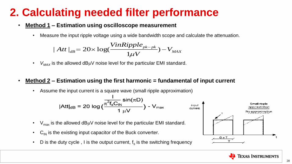
2. Calculating needed filter performance
28
• Method 1 – Estimation using oscilloscope measurement
• Measure the input ripple voltage using a wide bandwidth scope and calculate the attenuation.
• VMAX is the allowed dBμV noise level for the particular EMI standard.
• Method 2 – Estimation using the first harmonic = fundamental of input current
• Assume the input current is a square wave (small ripple approximation)
• Vmax is the allowed dBμV noise level for the particular EMI standard.
• CIN is the existing input capacitor of the Buck converter.
• D is the duty cycle , I is the output current, fs is the switching frequency
MAX
pkpk
dB VV
VinRippleAtt −=
−)
1log(20||
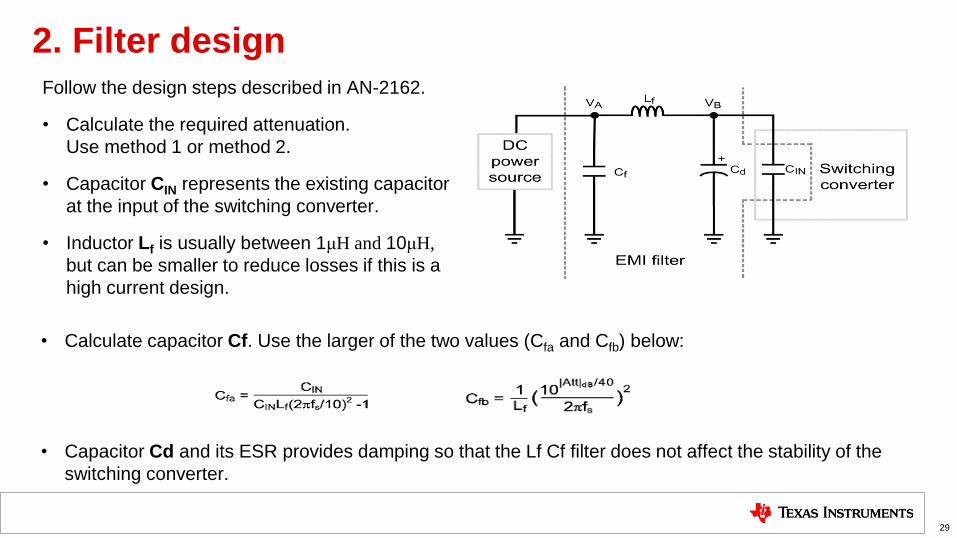
2. Filter design
29
Follow the design steps described in AN-2162.
• Calculate the required attenuation.
Use method 1 or method 2.
• Capacitor CIN represents the existing capacitor
at the input of the switching converter.
• Inductor Lf is usually between 1μH and 10μH,
but can be smaller to reduce losses if this is a
high current design.
• Calculate capacitor Cf. Use the larger of the two values (Cfa and Cfb) below:
• Capacitor Cd and its ESR provides damping so that the Lf Cf filter does not affect the stability of the
switching converter.
Car Metal Chassis
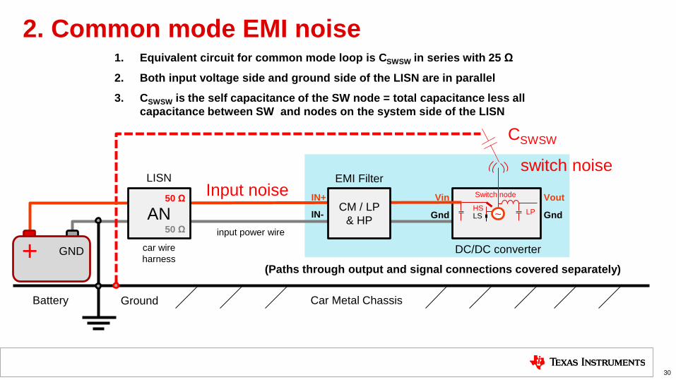
2. Common mode EMI noise
30
Ground
input power wire
DC/DC converter
CM / LP
& HP
EMI Filter
AN
GND+
LISN
Battery
Vin
Gnd
Vout
Gnd
IN+
IN-
car wire
harness
Input noise Switch node
HSLS
LP~
switch noise
1. Equivalent circuit for common mode loop is CSWSW in series with 25 Ω
2. Both input voltage side and ground side of the LISN are in parallel
3. CSWSW is the self capacitance of the SW node = total capacitance less all
capacitance between SW and nodes on the system side of the LISN
CSWSW
50 Ω
50 Ω
(Paths through output and signal connections covered separately)
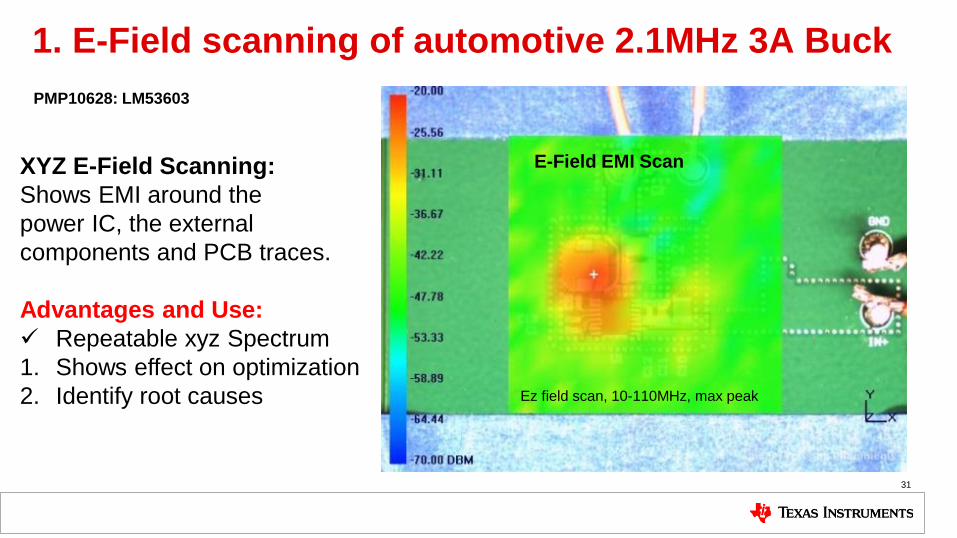
1. E-Field scanning of automotive 2.1MHz 3A Buck
31
PMP10628: LM53603
Ez field scan, 10-110MHz, max peak
E-Field EMI ScanXYZ E-Field Scanning:
Shows EMI around the
power IC, the external
components and PCB traces.
Advantages and Use:
✓ Repeatable xyz Spectrum
1. Shows effect on optimization
2. Identify root causes
Car Metal Chassis
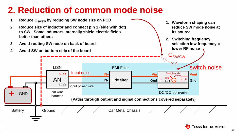
2. Reduction of common mode noise
32
Ground
input power wire
GND+
Battery
Gnd
Input noiseswitch noise
1. Reduce CSWSW by reducing SW node size on PCB
2. Reduce size of inductor and connect pin 1 (side with dot)
to SW. Some inductors internally shield electric fields
better than others
3. Avoid routing SW node on back of board
4. Avoid SW on bottom side of the board
CSWSW
AN
LISN
car wire
harnessDC/DC converter
Vin Vout
Gnd
Switch node
HSLS
LP~Pie filter
IN+
IN-
EMI Filter
1. Waveform shaping can
reduce SW mode noise at
its source
2. Switching frequency
selection low frequency =
lower RF noise
50 Ω
50 Ω
(Paths through output and signal connections covered separately)

Car Metal Chassis
2. Reduction of common mode noise
33
Ground
input power wire
GND+
Battery
Gnd
Input noise
switch noise
CSWSW
1. Interrupt circuit by installing a shield connected to
ground on system side of the filter
2. Tall components near SW can act as a partial shield
AN
LISN
car wire
harnessDC/DC converter
Vin Vout
Gnd
Switch node
HSLS
LP~Pie filter
IN+
IN-
EMI Filter
Common mode
choke can break
common mode
circuit
50 Ω
50 Ω
(Paths through output and signal connections covered separately)

Car Metal Chassis
2. Common mode EMI noise, other outputs
34
Ground
input power wire
DC/DC converter
CM / LP
& HP
EMI Filter
AN
GND+
LISN
Battery
Vin
Gnd
Vout
Gnd
IN+
IN-
car wire
harness
Input noise Switch node
HSLS
LP~
50 Ω
50 Ω
1. External load capacitance can couple to ground external to the
system creating a common mode circuit
2. If external load ground connections is not close to input ground,
ground plane currents can generate ground noise which is seen as
common mode noise on the input
3. Signal connections act the same way
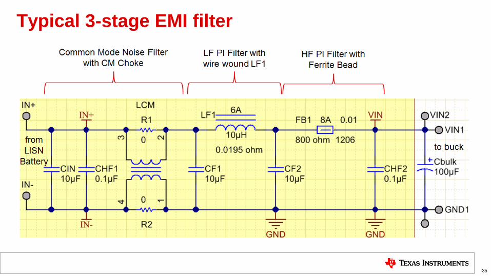
Typical 3-stage EMI filter
35

2.1MHz 3A Buck LM53603 – with 2-stage filter
36
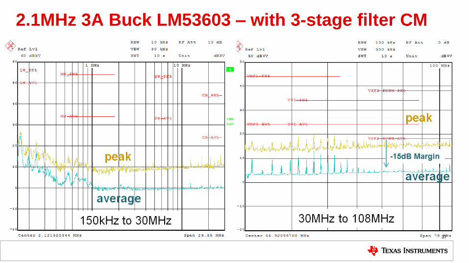
2.1MHz 3A Buck LM53603 – with 3-stage filter CM
37
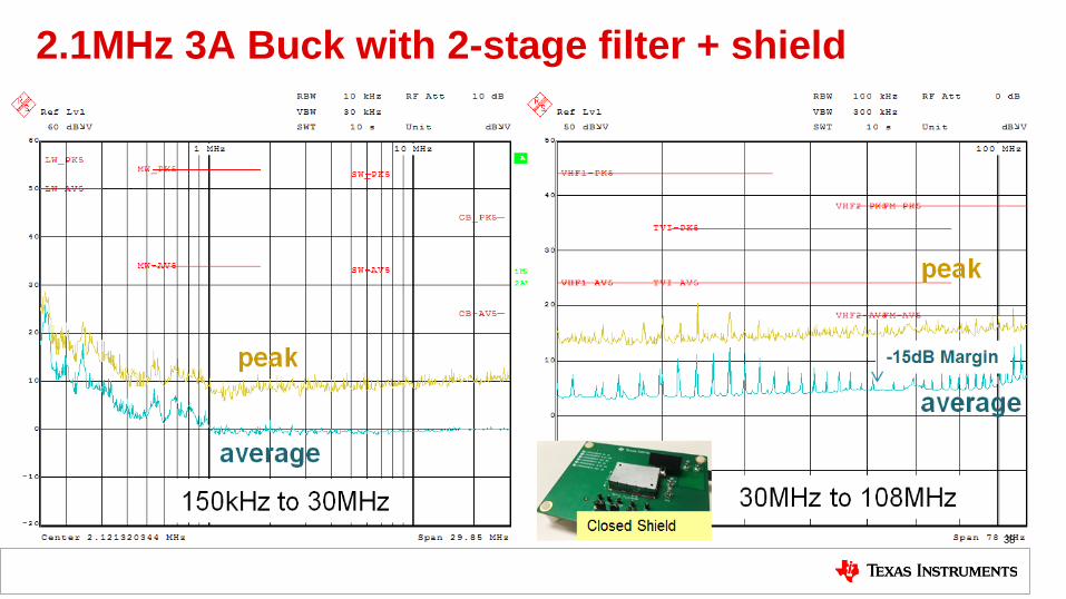
2.1MHz 3A Buck with 2-stage filter + shield
38

Pseudo random spread spectrum
Oscilloscope time domain 10ns per div
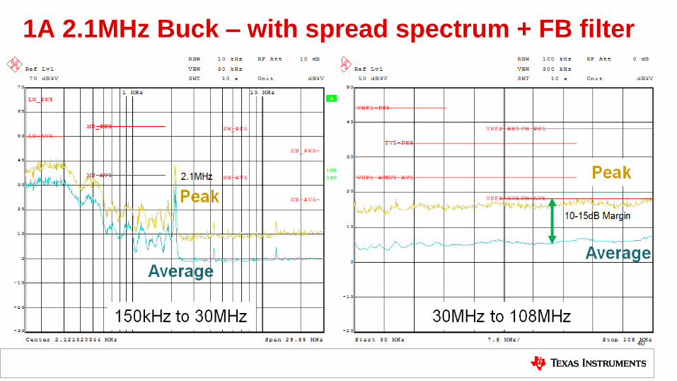
1A 2.1MHz Buck – with spread spectrum + FB filter
40
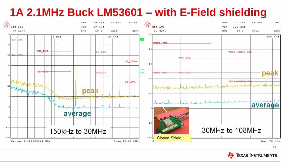
1A 2.1MHz Buck LM53601 – with E-Field shielding
41
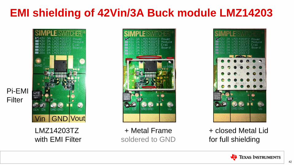
EMI shielding of 42Vin/3A Buck module LMZ14203
42
+ closed Metal Lid
for full shielding
+ Metal Frame
soldered to GND
LMZ14203TZ
with EMI Filter
Vin GND Vout
Pi-EMI
Filter
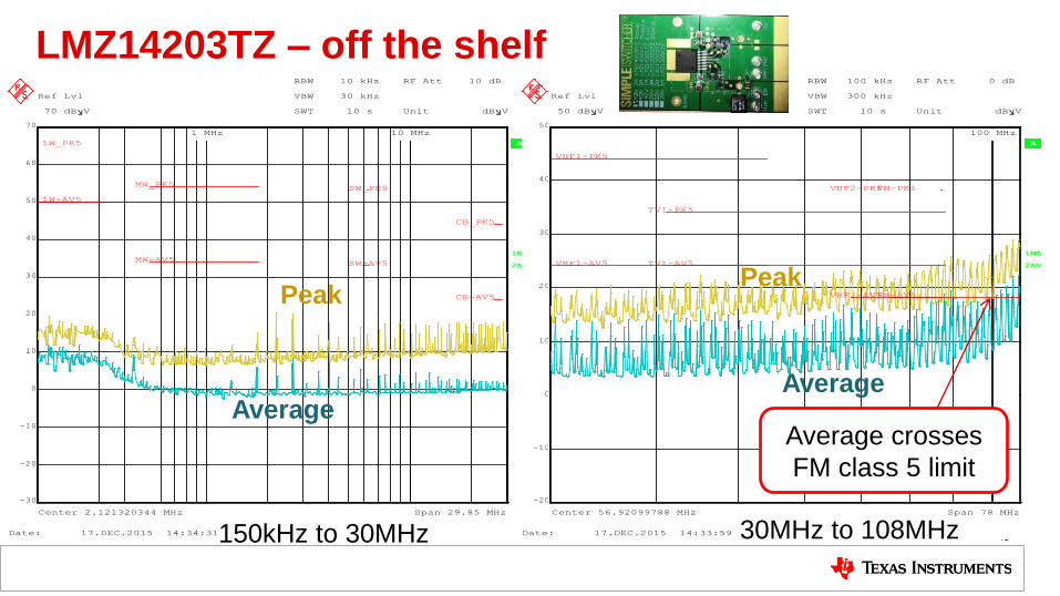
LMZ14203TZ – off the shelf
43
Ref Lvl
70 dBV
Ref Lvl
70 dBV
RBW 10 kHz
VBW 30 kHz
SWT 10 s
RF Att 10 dB
A
1MA
2AV2AV
Unit dBV
Center 2.121320344 MHz Span 29.85 MHz
1 MHz 10 MHz
-20
-10
0
10
20
30
40
50
60
-30
70
CB-AV5
LW_PK5
MW_PK5SW_PK5
LW-AV5
MW-AV5SW-AV5
CB_PK5
Date: 17.DEC.2015 14:34:31
Ref Lvl
50 dBV
Ref Lvl
50 dBV
RBW 100 kHz
VBW 300 kHz
SWT 10 s
RF Att 0 dB
A
1MA
2AV2AV
Unit dBV
Center 56.92099788 MHz Span 78 MHz
100 MHz
-10
0
10
20
30
40
-20
50
TVI-PK5
VHF1-PK5
VHF2-PK5
FM-AV5
FM-PK5
TVI-AV5VHF1-AV5
VHF2-AV5
Date: 17.DEC.2015 14:33:59
Average
Peak
Average
Peak
150kHz to 30MHz 30MHz to 108MHz
Average crosses
FM class 5 limit
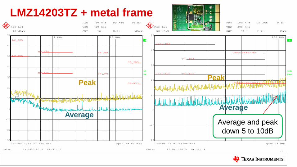
LMZ14203TZ + metal frame
44
Ref Lvl
70 dBV
Ref Lvl
70 dBV
RBW 10 kHz
VBW 30 kHz
SWT 10 s
RF Att 10 dB
A
1MA
2AV2AV
Unit dBV
Center 2.121320344 MHz Span 29.85 MHz
1 MHz 10 MHz
-20
-10
0
10
20
30
40
50
60
-30
70
CB-AV5
LW_PK5
MW_PK5SW_PK5
LW-AV5
MW-AV5SW-AV5
CB_PK5
Date: 17.DEC.2015 14:31:56
Ref Lvl
50 dBV
Ref Lvl
50 dBV
RBW 100 kHz
VBW 300 kHz
SWT 10 s
RF Att 0 dB
A
1MA
2AV2AV
Unit dBV
Center 56.92099788 MHz Span 78 MHz
100 MHz
-10
0
10
20
30
40
-20
50
TVI-PK5
VHF1-PK5
VHF2-PK5
FM-AV5
FM-PK5
TVI-AV5VHF1-AV5
VHF2-AV5
Date: 17.DEC.2015 14:32:59
Average
Peak
Average
Peak
Average and peak
down 5 to 10dB
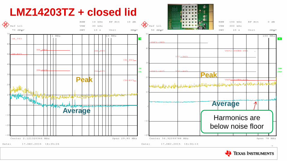
LMZ14203TZ + closed lid
45
Ref Lvl
70 dBV
Ref Lvl
70 dBV
RBW 10 kHz
VBW 30 kHz
SWT 10 s
RF Att 10 dB
A
1MA
2AV2AV
Unit dBV
Center 2.121320344 MHz Span 29.85 MHz
1 MHz 10 MHz
-20
-10
0
10
20
30
40
50
60
-30
70
CB-AV5
LW_PK5
MW_PK5SW_PK5
LW-AV5
MW-AV5SW-AV5
CB_PK5
Date: 17.DEC.2015 14:35:26
Ref Lvl
50 dBV
Ref Lvl
50 dBV
RBW 100 kHz
VBW 300 kHz
SWT 10 s
RF Att 0 dB
A
1MA
2AV2AV
Unit dBV
Center 56.92099788 MHz Span 78 MHz
100 MHz
-10
0
10
20
30
40
-20
50
TVI-PK5
VHF1-PK5
VHF2-PK5
FM-AV5
FM-PK5
TVI-AV5VHF1-AV5
VHF2-AV5
Date: 17.DEC.2015 14:36:13
Average
Peak
Average
Peak
Harmonics are
below noise floor
46