reliability issues and design solutions in advanced cmos
TRANSCRIPT

Reliability Issues and Design Solutions in Advanced CMOS Design
by
Ankita Bansal
A Thesis Presented in Partial Fulfillment
of the Requirements for the Degree
Master of Science
Approved June 2016 by the
Graduate Supervisory Committee:
Yu Cao, Chair
Hugh Barnaby
Jae-sun Seo
ARIZONA STATE UNIVERSITY
August 2016
brought to you by COREView metadata, citation and similar papers at core.ac.uk
provided by ASU Digital Repository

i
ABSTRACT
Over decades, scientists have been scaling devices to increasingly smaller feature
sizes for ever better performance of complementary metal-oxide semiconductor (CMOS)
technology to meet requirements on speed, complexity, circuit density, power consumption
and ultimately cost required by many advanced applications. However, going to these ultra-
scaled CMOS devices also brings some drawbacks. Aging due to bias-temperature-
instability (BTI) and Hot carrier injection (HCI) is the dominant cause of functional failure
in large scale logic circuits. The aging phenomena, on top of process variations, translate
into complexity and reduced design margin for circuits. Such issues call for “Design for
Reliability”. In order to increase the overall design efficiency, it is important to (i) study
the impact of aging on circuit level along with the transistor level understanding (ii)
calibrate the theoretical findings with measurement data (iii) implementing tools that
analyze the impact of BTI and HCI reliability on circuit timing into VLSI design process
at each stage. In this work, post silicon measurements of a 28nm HK-MG technology are
done to study the effect of aging on Frequency Degradation of digital circuits. A novel
voltage controlled ring oscillator (VCO) structure, developed by NIMO research group is
used to determine the effect of aging mechanisms like NBTI, PBTI and SILC on circuit
parameters. Accelerated aging mechanism is proposed to avoid the time consuming
measurement process and extrapolation of data to the end of life thus instead of predicting
the circuit behavior, one can measure it, within a short period of time. Finally, to bridge
the gap between device level models and circuit level aging analysis, a System Level
Reliability Analysis Flow (SyRA) developed by NIMO group, is implemented for a TSMC
65nm industrial level design to achieve one-step reliability prediction for digital design.

ii
DEDICATION
To my parents.

iii
ACKNOWLEDGMENTS
I would like to thank all the people who contributed in some way to the work
described in this thesis. First and foremost, I thank my academic advisor, DR. Yu Cao, for
accepting me into his group. During my thesis, he contributed to a rewarding graduate
school experience by giving me intellectual freedom in my work, supporting my attendance
at various conferences, engaging me in new ideas, and demanding a high quality of work
in all my endeavors. Additionally, I would like to thank my committee members Professor
Dr. Hugh Barnaby and Dr. Jae-Sun-Seo for their interest in my work.
Every result described in this thesis was accomplished with the help and support of
fellow labmates and collaborators. Ketul Sutaria gave me his valuable guidance and
constructive suggestions. Abinash Mohnaty and I worked together on several different
phases of the project, and without his efforts my job would have undoubtedly been more
difficult. I greatly benefited from his keen scientific insight, his knack for solving
seemingly intractable practical difficulties, and his ability to put complex ideas into simple
terms. I would also like to acknowledge othe members of NIMO group who extended their
support from time to time : Naveen Suda, Venkat Ravi, Zihan Xu, Devyani Patra.
Many friends and family have helped overcome setbacks and stay focused on my
graduate study. I greatly value their friendship and I deeply appreciate their belief in me.
Though only my name appears on the cover of this dissertation, a great many people have
contributed to its production. I owe my gratitude to all those people who have made this
dissertation possible and because of whom my graduate experience has been one that I will
cherish forever.

iv
TABLE OF CONTENTS
Page
LIST OF TABLES ................................................................................................................... vi
LIST OF FIGURES ............................................................................................................... vii
CHAPTER
1 INTRODUCTION ................. .................................................................................... 1
1.1 Overview : Reliability Issues in CMOS Design ................................. 1
1.2 Impact of Aging at Device and Circuit Level ..................................... 4
1.3 Thesis Contribution .............................................................................. 6
1.4 Thesis Organization.…….…………………………………………7
2 AGING MEASUREMENTS FOR DIGITAL CIRCUITS ....................................... 8
2.1 Introduction .......................................................................................... 8
2.2 Discrete Device Characterization ........................................................ 9
2.3 VCO Measurement Methodology ..................................................... 10
2.4 Test Plan for 28nm HKMG VCO ………………………………..11
2.5 Measurement Results …………………………………………….13
2.6 Accelerated Aging ………………………………………………16
3 SYRA FOR CIRCUIT AGING ANALYSIS ........................................................... 17
3.1 Introduction ....................................................................................... 17
3.2 Previous Work ................................................................................... 18
3.3 Asymmetric Aging ............................................................................ 19
3.4 Gate Level Aging Model……..…………………………………...21
3.5 Simulation Method………………………………………………..23
v
CHAPTER Page
3.6 SyRA with Industrial Level Design……...………………………25
4 SUMMARY ..............................................................................................................34
REFERENCES .....................................................................................................35
vi
LIST OF TABLES
Table Page
1. Delay Comparison for Top 5 Critical Paths ......................................................... 31

vii
LIST OF FIGURES
Figure Page
1.1. Reliability Effects seen with Increase in Operation Time ........................... 2
1.2. Impact on Threshold Voltage and Mobility with Aging due to NBTI …. .. 4
1.3. Impact on Threshold Voltage with Aging due to HCI ................................ 4
1.4. Shift in the Frequency of 21 Stage Ring Oscillator due to NBTI ............... 5
2.1. IV Curves for NMOS at Room Temperature ………. ................................ 9
2.2. IV Curves for PMOS at Room Temperature ............................................... 9
2.3. VCO Structure to Study the Effect of NBTI on Circuit Frequency ……. 10
2.4. Packaging Options for VCO Structures of Varied Dimensions ................ 11
2.5. VCO1: 1.8V ANALOG PMOS ; Size: 1000nm X 1000nm
VCO5: 1.8V ANALOG PMOS ; Size: 1000nm X 150nm ………. ........ 11
2.6. VCO2: 0.9V ANALOG DNW Reg Vt NMOS ; Size: 300nm X 30nm
VCO8: 0.9V ANALOG DNW Reg Vt NMOS ; Size: 600nm X 60nm . 11
2.7. VCO3: 1.8V ANALOG NMOS ; Size: 1000nm X 150nm ………...….12
2.8. VCO4: 0.9V ANALOG DNW Reg Vt PMOS ; Size: 1000nm X 1000nm
VCO6: 0.9V ANALOG DNW Reg Vt PMOS ; Size: 600nm X 60nm
VCO7: 0.9V ANALOG DNW Reg Vt PMOS ; Size: 300nm X 30nm . .12
2.9. Post Silicon Measurements for (a) VCO4 (b) VCO7 at Room
Temperature …………………………………………………………….13
2.10. Post Silicon Measurements for VCO3 at Room Temperature ................... 14
2.11. Long term High Temperature Stress Measurement on a VCO, Showing
the Effect of NBTI on RO Frequency ......................................................... 14
viii
Figure Page
3.1. Timing Analysis under Aging Effect using SyRA Tool ............................ 23
3.2. Change in Vth with Time due to Static/Dynamic NBTI Sress on 65nm . 26
3.3. Change in Vth with Time due to Static/Dynamic HCI Stress on 65nm .... 27
3.4. NBTI and HCI Aging Model for both Static and Dynamic Stress Case
and their Comparison with Traditional Industry Aging Model ................. 28
3.5. Industry Aging and SyRA Aging Comparison ………. ............................ 32
3.6. Delay Comparison for Different Switching Activity ................................. 33

1
CHAPTER 1
INTRODUCTION
1.1 Overview: Reliability Issues in CMOS Design
Moore’s law in predicting the increase in no. of transistor by ~2X rate in every two
years [1] has been the driving force for technological advancement and innovation in the
semiconductor industry for over 5 decades. I happened to survive as a self-fulfill this
prophecy. Most other fields of engineering involve tradeoffs between performance, power,
and price. However, as transistors become smaller, they also become faster, dissipate less
power, and are cheaper to manufacture. This synergy has not only revolutionized
electronics, but also society at large.
A failure is a deviation from compliance with the system specification for a given period
of time. Failures are caused by faults, which are defined as failures of subsystems. Faults
have many causes, ranging from design bugs to manufacturing defects to wearout to
external disturbances to intentional abuse of a product. Not all faults lead to errors; some
are masked. For example, a bug in the multiprocessor interface logic does not cause an
error in a single-processor system. A defective via may go unnoticed if it is in parallel with
a good one. Studying the underlying faults gives insight into predicting and improving the
failure rate of the overall system. As gate oxides are subjected to stress, they gradually
wear out, causing the threshold voltage to shift and the gate leakage to increase. Eventually,
the circuit fails because transistors become too slow, mismatches become too large, or
leakage currents become too great. Processes generally specify a maximum operating
voltage to ensure oxide wearout effects are limited during the lifetime of a chip. The
primary mechanisms for oxide wearout include the following:
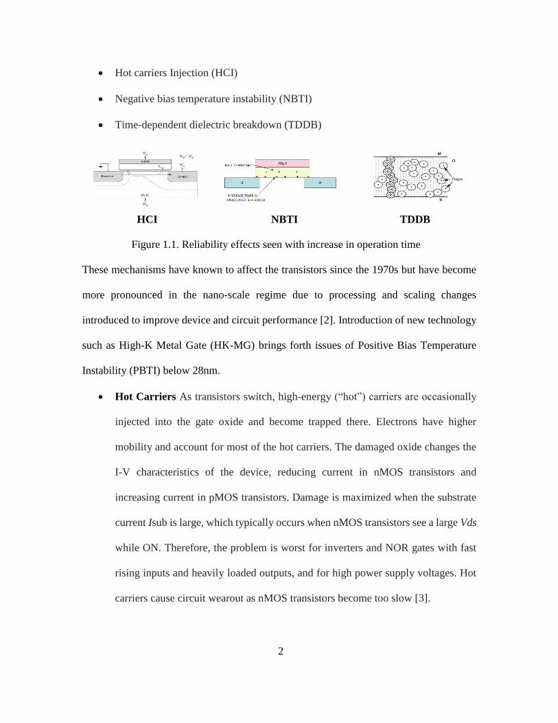
2
Hot carriers Injection (HCI)
Negative bias temperature instability (NBTI)
Time-dependent dielectric breakdown (TDDB)
HCI NBTI TDDB
Figure 1.1. Reliability effects seen with increase in operation time
These mechanisms have known to affect the transistors since the 1970s but have become
more pronounced in the nano-scale regime due to processing and scaling changes
introduced to improve device and circuit performance [2]. Introduction of new technology
such as High-K Metal Gate (HK-MG) brings forth issues of Positive Bias Temperature
Instability (PBTI) below 28nm.
Hot Carriers As transistors switch, high-energy (“hot”) carriers are occasionally
injected into the gate oxide and become trapped there. Electrons have higher
mobility and account for most of the hot carriers. The damaged oxide changes the
I-V characteristics of the device, reducing current in nMOS transistors and
increasing current in pMOS transistors. Damage is maximized when the substrate
current Isub is large, which typically occurs when nMOS transistors see a large Vds
while ON. Therefore, the problem is worst for inverters and NOR gates with fast
rising inputs and heavily loaded outputs, and for high power supply voltages. Hot
carriers cause circuit wearout as nMOS transistors become too slow [3].

3
Negative Bias Temperature Instability When an electric field is applied across a
gate oxide, dangling bonds called traps develop at the Si-SiO2 interface. The
threshold voltage increases as more traps form, reducing the drive current until the
circuit fails. The process is most pronounced for pMOS transistors with a strong
negative bias (i.e., a gate voltage of 0 and source voltage of VDD) at elevated
temperature. It has become the most important oxide wearout mechanism for many
nanometer processes [3].
Time-Dependent Dielectric Breakdown As an electric field is applied across the
gate oxide, the gate current gradually increases. This phenomenon is called time-
dependent dielectric breakdown (TDDB) and the elevated gate current is called
stress-induced leakage current (SILC). The exact physical mechanisms are not
fully understood, but TDDB likely results from a combination of charge injection,
bulk trap state generation, and trap-assisted conduction[Hicks08]. After sufficient
stress, it can result in catastrophic dielectric breakdown that short-circuits the gate
[3].
4
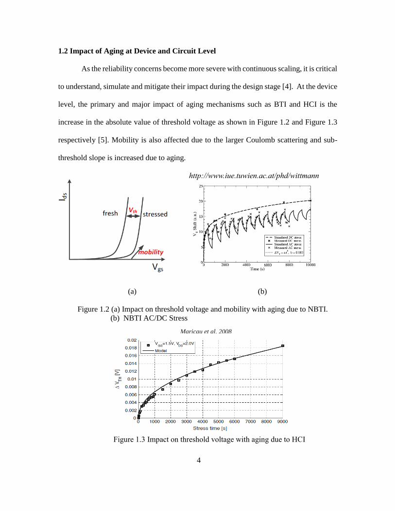
1.2 Impact of Aging at Device and Circuit Level
As the reliability concerns become more severe with continuous scaling, it is critical
to understand, simulate and mitigate their impact during the design stage [4]. At the device
level, the primary and major impact of aging mechanisms such as BTI and HCI is the
increase in the absolute value of threshold voltage as shown in Figure 1.2 and Figure 1.3
respectively [5]. Mobility is also affected due to the larger Coulomb scattering and sub-
threshold slope is increased due to aging.
http://www.iue.tuwien.ac.at/phd/wittmann
(a) (b)
Figure 1.2 (a) Impact on threshold voltage and mobility with aging due to NBTI.
(b) NBTI AC/DC Stress
Figure 1.3 Impact on threshold voltage with aging due to HCI
Maricau et al. 2008
5
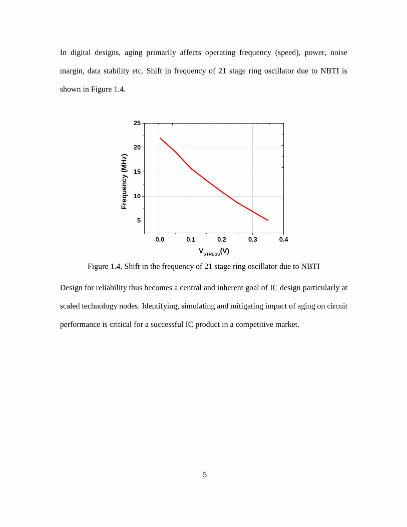
In digital designs, aging primarily affects operating frequency (speed), power, noise
margin, data stability etc. Shift in frequency of 21 stage ring oscillator due to NBTI is
shown in Figure 1.4.
0.0 0.1 0.2 0.3 0.4
5
10
15
20
25F
req
ue
nc
y (
MH
z)
VSTRESS
(V)
Figure 1.4. Shift in the frequency of 21 stage ring oscillator due to NBTI
Design for reliability thus becomes a central and inherent goal of IC design particularly at
scaled technology nodes. Identifying, simulating and mitigating impact of aging on circuit
performance is critical for a successful IC product in a competitive market.

6
1.3 Thesis Contribution
BTI and HCI aging effect are dominant aging mechanisms that affect circuit
operation over lifetime. BTI in both PMOS and NMOS devices exhibits stress and recovery
behavior which presents a unique challenge. Static aging models are needed for devices
under constant stress. Whereas, the device under dynamic stress, like the current circuits
under DVS, need a dynamic model (stress and recovery) for BTI (HCI show no recovery).
In this work, the effect of NBTI, PBTI and SILC is studied on a 28nm HKMG ring-
oscillator structure for various device dimensions. A constant shift in frequency of the ring
oscillator structure, with the static stress of the header/tail PMOS/NMOS device is noticed
owing to NBTI and PBTI respectively, Simulations are done by adding a resistance
between gate and drain to emulate the effect of SILC in digital circuits and it is observed
that the RO frequency decrease with time under SILC effect. In the second stage of thesis,
a system reliability tool (SyRA) developed by the NIMO research group is implemented
on an industrial level design of ~5000 gates and proven to be more realistic than the
traditional aging analysis mechanism used by people to study the impact of aging on circui
timing.

7
1.4 Thesis Organization
The organization of the thesis report is as follows: Chapter two presents the post
silicon measurement results of 28nm HKMG VCO structure. Results indicate the
frequency shift of the RO frequency under the effect of NBTI, PBTI and SILC. Chapter 3
explains the SyRA methodology used for circuit aging analysis and the implementation of
SyRA on an industrial level design. Chapter 4 summarizes the report as well as the future
work need to be carried out.

8
CHAPTER 2
AGING MEASUREMENTS IN DIGITAL CIRCUITS
2.1 Introduction
Aging due to bias-temperature-instability (BTI) is the dominant cause of functional
failure in large scale logic circuits. Power efficient techniques such as clock gating or
dynamic voltage scaling exacerbate the problem of asymmetric aging [6]. This work
highlights the impact of NBTI and PBTI at advanced technology node on frequency shift
which in turn leads to delay increase and thus results in timing violations in digital circuits.
The contributions of this work is the post Silicon demonstration of monotonic shift of
frequency under static stress condition due to NBTI, PBTI and SILC effect. To study the
effect of aging in digital circuit, silicon data is measured from 28nm ring oscillator (RO).
The frequency change of RO is measured as a direct index of the degradation, which is
proportional to PMOS threshold voltage change under NBTI and NMOS threshold voltage
under PBTI. Figure 2.3 presents the test circuit of Voltage Controlled Ring Oscillator
(VCO) structure used for aging analysis. Frequency change in 21 stage ring oscillator is
monitored during the test. The ring oscillator is activated by control (VCONTROL) pin.
Different from traditional RO based aging test, this test structure has a head (PMOS) or tail
(NMOS) device to make it emulate power gated circuits.

9
2.2. Discrete Device Characterization:
Nominal IV Curves: Characterization of 28nm HKMG discrete devices was
performed at nominal conditions for both PFET and NFET. Following are the IV
curves for the same for varied dimensions.
Figure 2.1: IV curves for NMOS at room temperature.
Figure 2.2: IV curves for PMOS at room temperature.
10
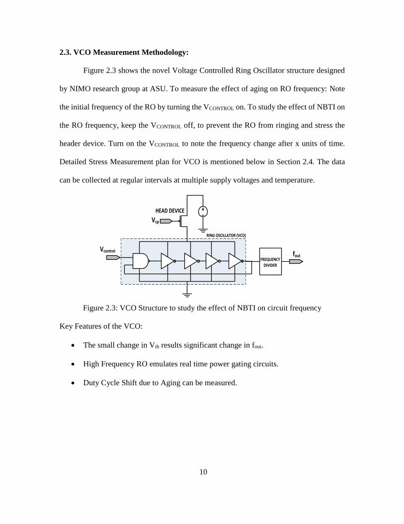
2.3. VCO Measurement Methodology:
Figure 2.3 shows the novel Voltage Controlled Ring Oscillator structure designed
by NIMO research group at ASU. To measure the effect of aging on RO frequency: Note
the initial frequency of the RO by turning the VCONTROL on. To study the effect of NBTI on
the RO frequency, keep the VCONTROL off, to prevent the RO from ringing and stress the
header device. Turn on the VCONTROL to note the frequency change after x units of time.
Detailed Stress Measurement plan for VCO is mentioned below in Section 2.4. The data
can be collected at regular intervals at multiple supply voltages and temperature.
Figure 2.3: VCO Structure to study the effect of NBTI on circuit frequency
Key Features of the VCO:
The small change in Vth results significant change in fout.
High Frequency RO emulates real time power gating circuits.
Duty Cycle Shift due to Aging can be measured.
RING OSCILLATOR (VCO)
HEAD DEVICE
Vcp
Vcontrol
FREQUENCY DIVIDER
fout

11
2.4 Test Plan for 28nm HKMG VCO
Packaging Options
Figure 2.4: Packaging options for VCO structures of varied dimensions
VCO1 / VCO5
Figure 2.5: VCO1: 1.8V ANALOG PMOS ; Size: 1000nm X 1000nm
VCO5: 1.8V ANALOG PMOS ; Size: 1000nm X 150nm
VCO2/VCO8
Figure 2.6: VCO2: 0.9V ANALOG DNW Reg Vt NMOS ; Size: 300nm X 30nm
VCO8: 0.9V ANALOG DNW Reg Vt NMOS ; Size: 600nm X 60nm

12
VCO3
Figure 2.7: VCO3: 1.8V ANALOG NMOS ; Size: 1000nm X 150nm
VCO4 / VCO6 / VCO7
Figure 2.8: VCO4: 0.9V ANALOG DNW Reg Vt PMOS ; Size: 1000nm X 1000nm
VCO6: 0.9V ANALOG DNW Reg Vt PMOS ; Size: 600nm X 60nm
VCO7: 0.9V ANALOG DNW Reg Vt PMOS ; Size: 300nm X 30nm
13
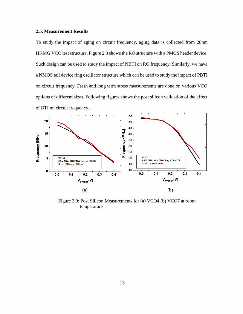
2.5. Measurement Results
To study the impact of aging on circuit frequency, aging data is collected from 28nm
HKMG VCO test structure. Figure 2.3 shows the RO structure with a PMOS header device.
Such design can be used to study the impact of NBTI on RO frequency. Similarly, we have
a NMOS tail device ring oscillator structure which can be used to study the impact of PBTI
on circuit frequency. Fresh and long term stress measurements are done on various VCO
options of different sizes. Following figures shows the post silicon validation of the effect
of BTI on circuit frequency.
(a) (b)
Figure 2.9: Post Silicon Measurements for (a) VCO4 (b) VCO7 at room
temperature

14
Figure 2.10: Post Silicon Measurements for VCO3 at room temperature
Long Term Stress Measurements
VCO4 test structure is kept for long term stress to study the impact of NBTI on RO
frequency. During Stress, keep all the voltages constant, VGATE = “1” (for Header PMOS
device) and stress the chip for a long duration of time at high temperature(by keeping the
board in Oven) and turn off the ringing of RO by turning off its enable signal.
Measure the frequency of RO at constant time interval by turning on the enable signal of
RO.
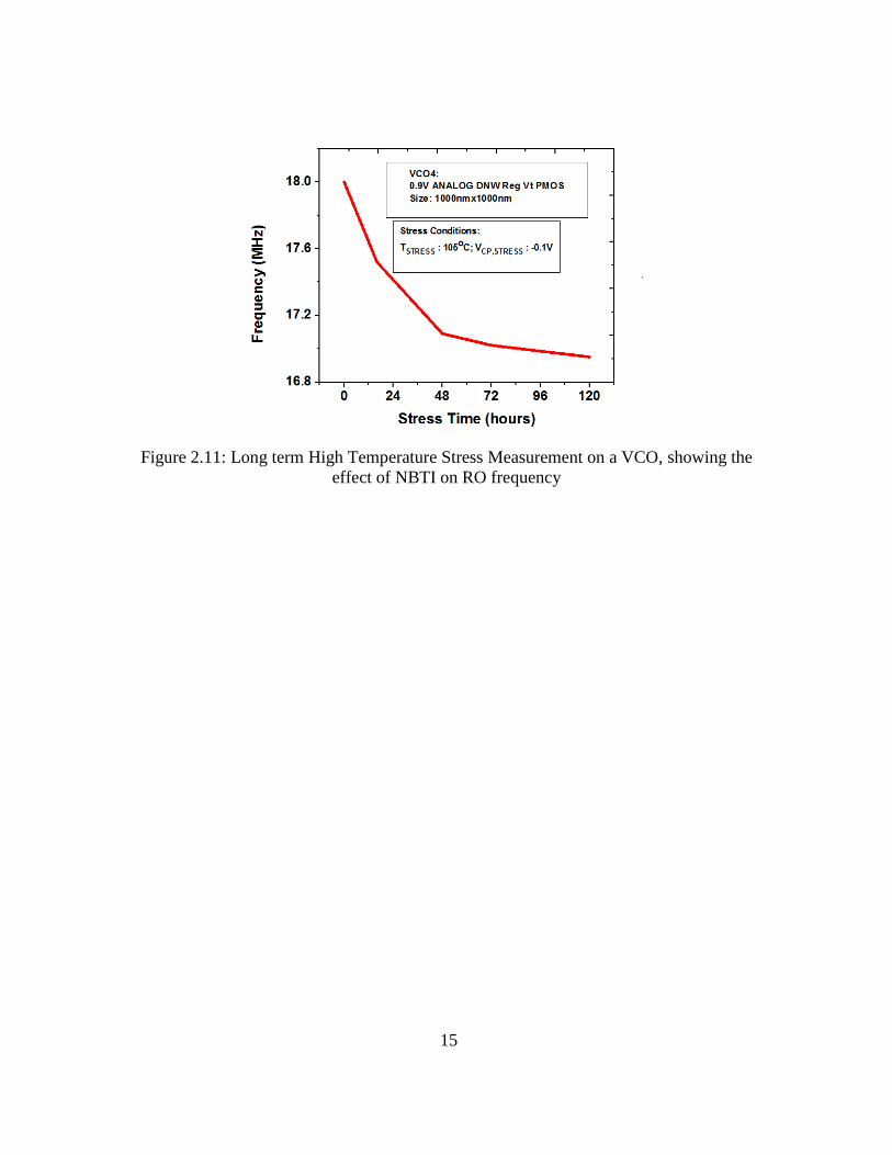
15
Figure 2.11: Long term High Temperature Stress Measurement on a VCO, showing the
effect of NBTI on RO frequency

16
2.4 Accelerated Aging
Aging mechanisms such as Bias Temperature Inversion (BTI) and Channel Hot
Carrier (CHC) are key limiting factors of circuit lifetime in CMOS design. Threshold
voltage shift due to degradation is usually a gradual process, causing a moderate rate of
increase in failure rate of CMOS design. In order to accurately test the degradation, it is
necessary to employ methods to accelerate the process of aging. This is done by using
elevated operating voltages and temperatures. It can also be done for closed loop
technologies that employ feedback for system stability or Dynamic Voltage Scaling (DVS).
Dynamically varying the operating voltage to compensate for slowing down due to aging
causes the device to degrade at a faster rate. Accelerated aging by identifying positive
feedback loops can help pinpoint weaknesses in a design.
Accelerated aging due to DVS can also be used for the benefit of the circuit design. End of
life characteristic of a design can be predicted by accelerating the aging in a controlled
manner. This would help avoid the time consuming measurement process and extrapolation
of data to the end of life thus instead of predicting the circuit behavior, one can measure it,
within a short period of time. Thus, acceleration of aging in a circuit helps in better
estimation of lifetime and to weed out the ones that may fail before expected lifetime.
In summary, this work illustrates the impact of NBTI and PBTI on frequency shift in a
voltage controlled ring oscillator design. Post Silicon measurements for 28nm HKMG
VCO structure is done for varied header and tail device sizes. Over the period of time, we
see a considerable amount of shift in circuit frequency due to BTI aging effect.

17
CHAPTER 3
SYRA FOR CIRCUIT AGING ANALYSIS
3.1 Introduction
Aging mechanism like NBTI, HCI manifests itself as the increase in threshold
voltage (Vth) of PMOS and NMOS, respectively [7]. It results in increase in gate and path
delay of digital circuits resulting in timing violations during circuit operations because
many critical paths which were not critical at the design stage, may turn critical over time.
The initial performance margins need to be increased to avoid such violations [8].
Therefore, it is essential to include impact of aging mechanism like NBTI and HCI in
circuit timing analysis to guarantee the circuit lifetime.
However, timing analysis under aging is not trivial since NBTI and HCI has a strong
dependence on technology specifications and operating conditions [7]. The analysis of
NBTI effect is more complex since NBTI exhibits both stress and recovery during dynamic
circuit operation. PMOS device under NBTI undergoes degradation or recovery depending
on the operating voltages. Traditional reliability analysis assumes constant stress
conditions and do not account for the more complex operating patterns in today’s digital
circuits, such as operating under constant stress (standby mode) for long periods of time
[7]. Hence, it is crucial to identify the critical moments in the operation pattern which have
maximum NBTI effect, thereby causing increased timing violations. Also, it is important
to take into account the effect of recovery on the change in threshold voltage of the device.
If we study NBTI only under constant stress, forgetting the operating conditions like
power-down mode, when the device goes in recovery, the results would be much
underestimated, making our design margin overly pessimistic.

18
3.2 Previous Works
Reliability tools such as BERT, RelXpert, etc. were used to evaluate performance
degradation in circuits. The main disadvantage of these tools are too many SPICE
parameters. Other drawbacks are change in operating conditions over time are not
considered.
For reliability analysis in digital circuits, several works have been proposed. Given the
delay of a digital gate, aging models are proposed to estimate the delay shifts [9]. These
delay models are complicated as they use Taylor series expansion and Chebyshev
polynomial to fit the gate delay degradation. Further, NBTI-based STA framework is
proposed in [10] using aging aware library. This STA analysis does not take into account
the effect of different workload for different gates. Along with addressing the above
limitations, this work focuses on aged timing analysis which is compatible and easily
integrated into the standard modeling/circuit analysis flow; supports large scale simulation
requiring minimum effort by the designer; and reduces the time involved in performing the
aging analysis.

19
3.3 Asymmetric Aging
In addition to predict the aging sensitivity to operating conditions, it is essential to
accurately predict the shift in path delay [11]. Previous works assume that NBTI effect is
averaged out due to alternate stress and recovery phases in the logic path or do not
differentiate between rising and falling transient edges [10], resulting in inaccurate
prediction in path delay shift. NBTI only affects the low to high (tpLH) delay of an
inverting gate (since PMOS Vth is shifted). Similarly, HCI affects only the high to low
delay of an inverting gate (since NMOS Vth is shifted). Threshold voltage shift (ΔVth) and
gate delay shifts (Δtd) are determined based on the circuit operation conditions and
environmental factors. Aging prediction for typical mobile and hand-held products is more
complicated as it involves long standby modes due to power reductions achieved through
clock gating. Traditional aging models handle such situations with an average activity to
estimate long term degradation. While a worst case analysis by assuming that all the gates
are under static stress is overly pessimistic [10], it is important to track the exact moment
when the circuit experiences maximum degradation.
In dynamic operation, PMOS devices are under alternate stress and recovery cycle, leading
to moderate degradation. When the circuit is operated in standby mode, PMOS transistor
is under static stress leading to much larger degradation. NBTI is a strong function of
average duty cycle. Similarly, HCI in NMOS is a strong function of output toggle rate and
the rise/fall time. SyRA focuses on the accurate failure diagnosis method for predicting
timing violations in sequential circuits under NBTI and HCI aging.
The key features of this work are:

20
It uses simple gate delay models to predict delay shift using long term ΔVth
predictive models. NBTI and HCI induced delay increase is calculated using delay
sensitivity to Vdd in standard cell library, avoiding complicated SPICE simulations
to predict aging in gate delays. The main advantage in this delay prediction method
is that the re-characterization of library standard cells under various aging scenarios
is not required and the previously characterized cell library can be used.
Asymmetric aging due to NBTI and HCI is taken into account by increasing the
TPLH due to NBTI and tPHL due to HCI.
This methodology takes into account the impact of various operating conditions
and workload (average duty cycle, toggle rate, rise/fall time) of gate delay aging.
SyRA is fully compatible with current circuit analysis flow and can handle as
complex and big a design as STA capability. It is tested on an industrial level design
of ~5000 gates.

21
3.4 Gate Level Aging Model
A simple gate delay model is presented here that calculates the delay change due to
ΔVth from Vdd information in the cell library. The proposed model is independent of the
load capacitance and input slew rates which impact the delay shifts. This model calculates
the delay degradation with time directly from the cell library, without having to rely on
expensive simulation to characterize the library under several aging conditions. Since the
primary impact of NBTI and HCI at the device level is the increase in Vth, the primary
effect at the circuit level is the increase in gate delay. The delay of a digital gate (td) is
expressed by [57]:
𝑡𝑑 ∝ 𝐶𝑉𝑑𝑑
𝑉𝑑𝑑 − 𝑉𝑡ℎ
Where C is the output capacitance of the gate. The change in gate delay when both Vdd
and Vth are subjected to change is:
∆𝑡𝑑
𝑡𝑑=
∆𝑉𝑑𝑑
𝑉𝑑𝑑−
∆𝑉𝑑𝑑−∆𝑉𝑡ℎ
𝑉𝑑𝑑−𝑉𝑡ℎ
The delay change when only Vth is changed (ΔtdVth) or only when Vdd is changed (ΔtdVdd):
∆𝑡𝑑𝑉𝑡ℎ
𝑡𝑑=
∆𝑉𝑡ℎ
𝑉𝑑𝑑−𝑉𝑡ℎ
∆𝑡𝑑𝑉𝑑𝑑
𝑡𝑑= −
∆𝑉𝑑𝑑∗𝑉𝑡ℎ
𝑉𝑑𝑑(𝑉𝑑𝑑−𝑉𝑡ℎ)
The above two equations can be combined to relate ΔtdVdd and ΔtdVth:
∆𝑡𝑑𝑉𝑡ℎ
𝑡𝑑= −
𝑉𝑑𝑑
𝑉𝑡ℎ(
∆𝑉𝑑𝑑
∆𝑉𝑡ℎ)) ∆𝑡𝑑𝑉𝑑𝑑
The above gate delay model calculates the change in delay due to threshold voltage shift
using the delay function of supply voltage. The proposed model predicts the shift in gate
delay in case of inverter and NAND gates where a single PMOS exists between switching

22
input and output, and also between Vdd and output. However, the situation is different in
gates like NOR, where there are multiple transistors between the switching input and
output.
𝑡𝑑𝑉𝑡ℎ = −𝑉𝑑𝑑
𝑉𝑡ℎ(
𝑘 ∑ ∆𝑉𝑡ℎ𝑖 + ∑ ∆𝑉𝑡ℎ𝑗𝑚𝑗=0
𝑁−𝑚𝑖=0
𝑁∆𝑉𝑑𝑑) ∆𝑡𝑑𝑉𝑑𝑑
Where k (~ 0.25) denotes the contribution of Vth of transistors not in the path of switching
input and output towards the delay shift compared to that from Vth of transistors in the
path of switching input and output.
23
3.5 Simulation Method
Aging analysis in a circuit can be implemented using SPICE, where each transistor is
replaced by the sub-circuit model of the aged device. For large circuits, replacing each
transistor with the sub circuits level is not practical and hence comes the need for gate level
timing analysis. Figure 3.1 presents the experimental setup and static timing analysis
framework implemented in this work.
Figure 3.1 Timing analysis under aging effect using SyRA tool
For a given digital circuit, we begin with the standard Static Timing Analysis (STA) which
generates fresh timing report with timing information of all the paths in the circuit, without
considering the any aging effect. Logic analysis is performed on the circuit to obtain
activity factors (α) in case of AC stress and node voltages in case of static stress. Based on
the stress conditions, PMOS and NMOS Vth shift and gate delay shifts are computed using
delay information from standard cell library under different slew rates and load
capacitances. Aged timing report is then obtained by updating gate and path delay shifts in
fresh timing report, thus identifying the paths violating timing requirements.
IEEE TRANSACTIONS ON DEVICE AND MATERIALS RELIABILITY, VOL. 13, NO. 2, JUNE 2013

24
This framework is generic and can be extended to other aging mechanisms such as Positive
Bias Temperature Instability (PBTI). It can be easily integrated into the standard STA flow.
The sizing and complexity of the circuit on which the aging analysis can be run using this
method directly depends on the STA capability being used. In this work, the
implementation of this aging flow is performed using PrimeTime, commercial STA tool
from Synopsys. The aging aware delay model captures the shift in the rising and the falling
delays of each gate in the circuit due to NBTI and HCI respectively. The non-critical paths
in the fresh circuit may turn critical over time due to aging, depending on the size of the
paths and types of gates.
25
3.6 SyRA with Industrial Level Design
SyRA was implemented on an industrial level design and to compare an industry’s
traditional aging analysis method with SyRA. Following are the highlights of the design
and the comparison results:
• Total number of gates in the given design: 50100
• Total no. of path in the design: 37239
• No. of paths under consideration for SyRA: 1039
• Simulation Time: 3~5 minutes (CPU info : Intel(R) Xeon(R) CPU E5-2650 v3 @
2.30GHz )
• % increase in Path Delay:
• SyRA Dynamic Aging ~ 10%
• Industry Aging ~ 19%
Traditional aging models at industry level does not take into account the recovery effect
for NBTI and the workload information for both NBTI and HCI.
For fair comparison, we calibrated our long term aging models (in static condition) with
the industrial aging model for NBTI and HCI models for PMOS and NMOS respectively.
ELDO simulator was used for the purpose. The equations obtained from this calibrations
are then used for Vth vs time curve for Static NBTI and HCI in SyRA. Fig3.2 and Fig 3.3
shows the calibration of SyRA long term static models with industry aging models for
NBTI and HCI. As we can see for dynamic models the Vth change is much less (more
optimistic) than the static aging which is being considered in conventional analysis.
Dynamic aging models takes into account the recovery and average duty cycle effect for
NBTI and toggle rate and rise/fall time information for HCI.

26
3.6.1 NBTI Aging Model
NBTI occurs when a high voltage is applied at the gate of a PMOS transistor at
elevated temperature and is explained based on the reaction-diffusion (RD) mechanism. In
NBTI, when a high negative electrical stress is applied at the gate of PMOS, interface
charges are generated at the Si-SiO2 interface. NBTI manifests itself as an increase in Vth.
Removal of stress anneals some of the interface traps resulting in partial recovery.
Temporal Degradation due to Static NBTI can be represented by the following equation:
∆𝑉𝑡ℎ𝑠 = 𝐾(𝑡)𝑛
Temporal Degradation due to dynamic NBTI, when considering recovery effect and
switching activity (average duty cycle) can be represented by:
∆𝑉𝑡ℎ𝑑 = 𝐾′(𝛼𝑡)𝑛
Where 𝛼 is the switching activity factor and n ~0.16 and K and K’ are technology constant.
Figure 3.2: Change in Vth with time due to static/dynamic NBTI stress for 65nm
27
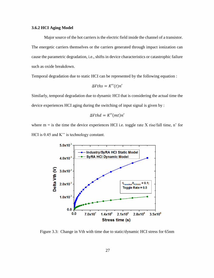
3.6.2 HCI Aging Model
Major source of the hot carriers is the electric field inside the channel of a transistor.
The energetic carriers themselves or the carriers generated through impact ionization can
cause the parametric degradation, i.e., shifts in device characteristics or catastrophic failure
such as oxide breakdown.
Temporal degradation due to static HCI can be represented by the following equation :
∆𝑉𝑡ℎ𝑠 = 𝐾′′(𝑡)𝑛′
Similarly, temporal degradation due to dynamic HCI that is considering the actual time the
device experiences HCI aging during the switching of input signal is given by :
∆𝑉𝑡ℎ𝑑 = 𝐾′′(𝑚𝑡)𝑛′
where m = is the time the device experiences HCI i.e. toggle rate X rise/fall time, n’ for
HCI is 0.45 and K’’ is technology constant.
Figure 3.3: Change in Vth with time due to static/dynamic HCI stress for 65nm

28
Figure 3.4: NBTI and HCI Aging model for both Static and Dynamic stress case and their
comparison with traditional industry aging model

29
3.6.3 Gate Level Aging Model used in SyRA
As we already mentioned, NBTI occurs in PMOS and hence will affect the TPLH
and HCI occurs mainly in NMOS and therefor will affect TPHL. Primtime timing report has
the info for each cell, if the transition type is rising or falling. Therefore, following method
is used to calculate delay of each gate.
When the output node is rising, delay equation would be:
∆𝑡𝑑𝑉𝑡ℎ
𝑡𝑑= −
𝑉𝑑𝑑
𝑉𝑡ℎ(
∆𝑉𝑑𝑑
∆𝑉𝑡ℎ)) ∆𝑡𝑑𝑉𝑑𝑑
where, ∆tdVdd is ∆tPLH|Vdd and ΔVth is due to NBTI. And when the output node is falling,
ΔtdVdd is ΔtPHL|Vdd and ΔVth is due to HCI.

30
3.6.4 Library Information and Stress conditions
Throughout this implementation the following libraries and stress conditions are used.
• TSMC 65 nm Standard Cell Library :
• tcbn65gplushvtwc.db (Slow-Slow, 125C, 0.9V)
• TSMC Aging Library :
• vtss65gplushvtwc_aging.db (Build on above standard cell library)
• Stress conditions:
• VG,STRESS = 0.9V
• TSTRESS =125C
• Stress Time ~ 10years

31
3.6.5 Results
Aging induced shifts in the logic paths and clock buffers of sequential circuits result
in timing violations. Table 3.1 shows the delay comparison results for top 5 critical paths
between SyRA and industrial design. Column 3 shows the fresh timing obtained from
Primetime STA analysis. Column 4 shows the increased path delays calculated using
SyRA. Coulmn 5 shows the path delay increase using Industry aging models.
As we can see the industry aging models are pretty conservative in nature as they don’t
take into account the effect of recovery in NBTI and switching activity information for
both NBTI and HCI. Whereas, SyRA, considering both the effects while calculating the
effect of aging on circuit timing paths give much more optimistic numbers. Thus it saves
us from over gaurdbanding the design for reliability.
Table 3.1: Delay comparison for top 5 critical paths

32
Figure 3.5 shows the bar plot comparing the percentage increase in path delay by using
industry aging analysis and SyRA aging analysis
Figure 3.5 Industry aging and SyRA aging comparison.
As we can see the Industry aging can over-estimate the path delay as high as 60% more
than SyRA aging.
Also, in SyRA, instead of recalculating the path delay for different switching activity of
input gates, we can take the average switching activity of all the gates as 0.5 and calculate
the aging effect. This helps in keeping a set gaurdband while including the reliability effect
in circuit design. Figure 3.6 shows the comparison of actual switching activity at all the
gate input verses 0.5 average switching activity.

33
Figure 3.6: Delay comparison for different Switching Activity
As we can see, by keeping the switching activity as 0.5, the path delay only varies with
~10%. Thus we can keep a gaurdband on 10% around the actual path delay while
incorporating the aging effect during digital circuit analysis.
In SyRA simple analytical model to predict the aging-induced delay shifts in a
digital gate is presented. More realistic estimation of NBTI and HCI aging by including
switching activity and Rise/Fall time in the calculation of ΔVth . The aging prediction uses
the library cell delays without relying on re-characterization of the standard cell library.
Compatible and easily integrated into standard circuit analysis flow.
Lastly, SyRA aging is demonstrated aging a large scale industry level design and proven
to be more efficient in terms of accuracy due to more realistic modeling and less time
consuming as it avoid re-characterization of standard cell library for various aging
scenarios.

34
CHAPTER 4
SUMMARY
In summary, this work illustrates the impact of NBTI and PBTI on frequency shift
of a 28nm HKMG technology voltage controlled ring oscillator structure. Measurements
confirms that under DC stress, there is a monotonic shift in the circuit frequency. Thus
confirming that circuit timing is highly sensitive to aging mechanisms and there is a need
to do aging analysis in digital circuit at an early design stage to avoid any violations later.
Also, in order to accurately test the degradation, it is necessary to employ methods to
accelerate the process of aging. For this purpose, accelerated aging is suggested.
Acceleration of aging in a circuit helps in better estimation of lifetime and to weed out the
ones that may fail before expected lifetime. This can be done by using elevated operating
voltages and temperatures. It can also be done for closed loop technologies that employ
feedback for system stability or Dynamic Voltage Scaling (DVS).
Lastly, a system reliability analysis (SyRA) tool, which serves as a connecting link between
transistor aging models and path delays of a VLSI circuit is implemented on a large scale
industrial level design and proven to be more efficient in terms of accuracy by employing
the more realistic scenarios during aging calculation and less time consuming as it avoids
the lengthy standard cell library characterization process for different aging conditions.

35
REFERENCES
[1] C. Constantinescu, "Trends and challenges in VLSI circuit reliability," IEEE micro 4, pp. 14-19, 2003.
[2] "http://www.itrs.net, International technology roadmap for semiconductor".
[3] Maricau, Elie and a. G. Gielen, "CMOS Reliability Overview," Analog IC Reliability in Nanometer CMOS. Springer New York, pp. 15-35, 2013.
[4] R. Zheng, "Circuit aging prediction for low-power operation," CICC, pp. 427-430, 2009.
[5] "http://www.iue.tuwien.ac.at/phd/wittmann".
[6] K. B. Sutaria, "Duty cycle shift under static/dynamic aging in 28nm HK-MG technology," Reliability Physics Symposium (IRPS, 2015).
[7] M. Agarwal, B. C. Paul, M. Zhang and a. S. Mitra, "Circuit Failure Prediction and its Application to Transistor Aging," IEEE VLSI Test Symp, p. 277–286, 2007.
[8] Y. Wang, H. Luo, K. He, R. Luo, H. Yang and and Y. Xie, "Temperature-aware nbti modeling and the impact of input vector control on performance degradation," Design, Automation and Test in Europe Conference and Exhibition, p. 1–6, April 2007.
[9] B. C. Paul, K. Kang, H. Kufluoglu, M. A. Alam and K. Roy, " "Impact of NBTI on the temporal performance degradation of digital circuits," IEEE Electron Device Letters, pp. vol.26, no.8, pp. 560- 562, 2005.
[10] W. Wang, Z. Wei, S. Yang and a. Y. Cao, " An Efficient Method to Identify Critical Gates under Circuit Aging," Int. Conference on Computer Aided Design,, pp. 735-740, Nov. 2007.
[11] J. B. Velamala, "Failure analysis of asymmetric aging under NBTI," Device and Materials Reliability, IEEE Transactions on 13.2, pp. 340-349, 2013.