report - amazhindu.files.wordpress.com · this report gives an overview of the problem for ......
TRANSCRIPT

THE RADAR MOTION DETECTOR_Report | GDP
DESIGN
PROJECT
REPORT ALFRED MAZHINDU
Supervised By Dr R W Clarke
Date Submitted 04/04/2011

ALFRED MAZHINDU Page 2
Table of Contents SUMMARY ............................................................................................................................................ 4
CONTENTS ............................................................................................................................................ 4
INTRODUCTION .................................................................................................................................. 4
Aims and Objectives ........................................................................................................................... 5
Theory Background ............................................................................................................................ 5
TOP LEVEL DESIGN ............................................................................................................................ 5
The Block Diagram ............................................................................................................................. 5
Engineering Solutions ......................................................................................................................... 7
Building the µProcessor Circuit ...................................................................................................... 7
Gantt chart ........................................................................................................................................... 7
Meetings and Experiments .............................................................................................................. 7
INDIVIDUAL CONTRIBUTIONS ........................................................................................................ 8
1. Assembling The Signal Processing Circuit on the breadboard (Task 9) ..................................... 8
2. Designing the circuit in the Proteus ISIS (Task 10) .................................................................... 8
3. Designing the PCBs on Proteus ARES (Task 11) ....................................................................... 9
4 Order the PCB and the µprocessor (Task 12) ........................................................................... 12
Tasks Completed ............................................................................................................................... 13
Tasks Residual .................................................................................................................................. 13
CONCLUSION ..................................................................................................................................... 14
REFERENCES ..................................................................................................................................... 14
APPENDICES ...................................................................................................................................... 14
Calculations for the gain ....................................................................................................................... 16
Radar Equation.................................................................................................................................. 16
Frequency Calculations ..................................................................................................................... 17
Calculations for the resistors of the Low-pass filter ......................................................................... 17
Calculations for the Horn ...................................................................................................................... 18
Program Code ....................................................................................................................................... 20
List of Components (Parts and Values) ................................................................................................ 22
Resistors (All resistors are carbon film) ........................................................................................... 22
Capacitors ......................................................................................................................................... 22
Semi-conductors ................................................................................................................................ 22
Miscellaneous ................................................................................................................................... 23
Diodes ............................................................................................................................................... 23
Bill of Materials (Comparison of suppliers) ..................................................................................... 23

ALFRED MAZHINDU Page 3
Table of Figures Figure 1: Block Diagram....................................................................................... 6
Figure 2: Gantt chart ............................................................................................. 7
Figure 3: Breadboard Circuit testing .................................................................... 8
Figure 4: Analogue processing circuit (First Stage) ............................................. 9
Figure 5: Analogue signal processing PCB design (Second Stage) ..................... 9
Figure 6: Analogue signal processing PCB in ARES output view ..................... 10
Figure 7: : Finished Soldered PCB of Analogue Processing Circuit .................. 10 Figure 8: Analogue Signal Processing PCB Testing and Measurement Displaying the square wave .. 11
Figure 9: Digital signal µProcessor Stage 1 ....................................................... 11
Figure 10: PCB Design of Doppler Radar Control uProcessor Unit Stage 2 ..... 12
Figure 11: Doppler Radar Control uProcessor Unit on ARES output view ....... 12
Figure 12: The Finished uProcessor PCB soldered ............................................ 13
Figure 13: Antenna Gain ..................................................................................... 18
Figure 14: Antenna Design ................................................................................. 19
Figure 15: Antenna Design [2] ........................................................................... 19

ALFRED MAZHINDU Page 4
SUMMARY The radar motion detector project is a design to determine the speed of a target within a
predetermined range of greater than 20m utilising the Doppler radar principle. The antenna
gain of a Doppler module and frequency bandwidth for the radar system were determined.
The Doppler Module is a system that involves creating a signal, transmitting the signal and
receiving back the reflected signal. The received signals are processed consequently and the
output directed to the display where it is read. The construction of the breadboard prototype
based on 2nd
Order Voice Comms Filter and Comparator circuit was employed with some
few alterations to resistors on the low pass filter to equalise the desired frequency range. The
circuit was then tested and the result was a square wave to be fed into the µprocessor. The
circuit layout was simulated with Proteus software (ISIS & ARES) for the PCB design and
the PCB was prepared and components soldered on it. Antenna horn dimensions were
determined from antenna gain chart at 18dB and the horn antenna designed. Software
developments for the microcontroller are well done; the PIC16 is programmed to be able to
make sense of the signal based on its frequency. After processing the signal the PIC16 sends
an information signal to LCD which outputs the speed of the moving target. The group is
now in process of the casing the PCBs design and how to fit all the components together such
that the device is portable and easy to maintain when there is a fault without having to
dismantle the device.
CONTENTS This report gives an overview of the problem for the design team. It details the design
requirements and specifications. Technical specifications of the design are also covered in the
report. The report further details the progress made so far in the design and construction
process of the motion detector. The appendix to the report contains a task breakdown. This is
a project plan to be done by individual or subgroups of the group. The whole project schedule
is explained with attached Gantt chart. Also included in the Appendix are important
diagrams and calculations from other members of the group and list of parts used in the signal
processing circuit are provided.
INTRODUCTION Our group has been sub-contracted to SESAME Enterprises Inc., Which set out to develop a
range of motion detector- system based on the microwave Doppler-radar principle for a wide
range sensing and measuring applications. The unit we seek to develop will be suitable for
each of the intended applications together with signal processing hardware which can be
easily re-programmable to implement the range of detection functions required. The design
and construction should all fit in the budgetary constraint of £40 pounds to be used on
materials and services only obtainable from outside the school laboratories. Since our design
is for wide range applications, the initial design will be for a particular application with room
for alterations. For the software a programmable chip will be used. This will make it possible
to vary application parameters by simple changing the program code then general principles
of signal generation and processing will apply.

ALFRED MAZHINDU Page 5
Aims and Objectives
To design, build and test a radar motion detector unit.
To calculate suitable values and specifications for this system.
To appreciate how engineering solutions can be used to solve human inefficiency and
other problems
To develop good communication skills by working closely with other members of a
design team.
To develop the essence of time management applying it on this project as set point
For the Real Life in the Industry.
Theory Background
Doppler radars can measure the velocity of targets relative to the radar. A Radar System uses
a radio frequency electromagnetic signal reflected from a target to determine the speed of the
target. Signal reflection can be influenced by the factors below:
Material (what the target is made from e.g. aluminium, wood, steel etc.)
Size(the bigger the target the more the reflected signal)
Shape (the outside shell of the target (e.g. oval, rectangular etc.)
TOP LEVEL DESIGN The two major parts that create the top level design and these directs our method to the
project and each step should be undertaken. The next tasks are deliberated to be very vital:
Block Diagram.
Engineering Solutions
Gantt Chart
The Block Diagram
The above heading describes operational stages of the systems in blocks, realizing major
components within the stages. It is the amplification of the total package of the system that
gives an overall idea of the system operation that can be easily understood by a layman.
However, five main blocks were identified.
Our engineering design solution as a group was applied to the design and construction of the
speed capture Gunn or the motion detector unity.
Power Supply Unit (PSU): is a source of electric power. It powers the circuit
electrically enabling the Doppler module to transmit and receive the signal, and on the
other hand powering other parts of the circuit. 12 volts power supply will be used to
power the system.
Doppler Module: Transmits the analogue signal to the target and receives the
reflected signal from the target.
Regulator: controls the amount of voltage entering the comparator, PIC,and the LCD
display. The more sensitive comparator circuit will use a regulated supply of 5Volts.
PIC: receives digital signal then be programmed using Ccode to display the actual
vehicle speed on the LCD display.

ALFRED MAZHINDU Page 6
Figure 1: Block Diagram
Signal generator: This is in essence the Doppler Module. It comprises of the oscillator which
generates a signal and this signal is transmitted towards the target by a transmitter antenna and
then the target reflects the signal back to be received by the receiver antenna. The received
signals are mixed by the mixer to produce a Doppler Signal. The Doppler signal is filtered
through a Band Pass filter then compared to a pre-determined value by the comparator and
then processed as required by a µprocessor.
Band pass filter (Low pass and Band pass): Allows frequencies only within certain range
and attenuates frequencies outside that range. For this system it is between 300Hz and around
4.8 kHz.
Comparator: Analogue to Digital converter. Has the comparator and is therefore capable of
comparing and then converting to an analogue signal to digital before it’s fed to the
µProcessor.
µProcessor: The µcontroller acts as the brain of the device. It is programmed using C
language to display the target speed at the LCD upon receiving the signal.
Control: Enables the system to capture and calculate the speed of the target.
LCD display: LCD stands for crystal liquid display. This is where the speed of the target is
displayed. Final results are displayed on LCD through the use of some LEDs.
Transmit
Signal
Radar Doppler Module Unit
Doppler
Signal
Output Analogue processing
circuit
OSCILLATOR
SENDER
RECEIVER
MIXER
LOW
PASS
HIGH
PASS
COMPARAT
OR
(ADC)
DIGITAL SIGNAL µPROCESSOR
CONTROL
PANEL
(Switches)
POWER SUPPLY AND
REGULATOR
LCD DISPLAY km/hr.

ALFRED MAZHINDU Page 7
Engineering Solutions
Engineering decisions have been made about the important design solutions. Applications
were done on dimensions of antenna horn, frequency range for the Band pass filter, and sizes
or values of components to be used in the circuit and as well as PCBs sizes.
Building the µProcessor Circuit
We designed the PCBs and assembling the components on it. Generally our PCB sizes are as
follows (Analogue signal processor PCB = 9 × 5cm) and (µprocessor PCB = 7 × 7cm) Glen
was assigned to drill holes of the PCBs. We then built the circuit and tested the functionality
of it. We also added the Doppler signal using signal generator and this showed that the circuit
works properly as specified. The PIC PCB will be tested as soon as we finish working on it.
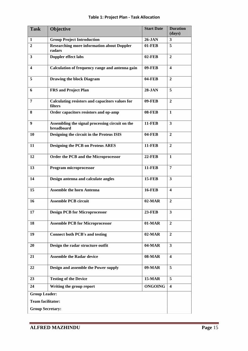
Gantt chart
The Gantt chart was used for planning purposes in this project. It reflects the distribution of
tasks amongst group members and also shows the progress of the project. It also gave the
group the ability to know whether we are on track with reference to time. Good management
skills can be applied using the Gantt chart. The Gantt chart on Figure 3 was designed by
Glen.
Figure 2: Gantt chart
Meetings and Experiments
Meetings were held to put all the individual ideas together, to go through researches, to check
progress of the project and individual strength and weaknesses in their allocated tasks. See
Table 1on appendix for the Project Plan.

ALFRED MAZHINDU Page 8
The group had a chance to develop an understanding of the Doppler Effect through laboratory
experiment of the Doppler module. It was observed that a Doppler signal is generated when
there is motion. The absence of a target means there is no reflection of the transmitted signal.
The presence of a target, in this case a moving object means the presence of a reflective
object within the range of transmission .The power of the received signal varies with
the angle, the distance, the cross section area and the speed of the target
This experiment contributed a greater understanding on how we should design our antenna.
Financial requirements were critically considered hence a budget was drawn up that makes
the project continue within the range of the budgeted £40. Order sheets were prepared to
order different components required see attached order sheet on appendix Table 2.
INDIVIDUAL CONTRIBUTIONS
1. Drawing the block Diagram (Task 5)
2. Assembling the signal processing circuit on the breadboard (Task 9 )
3. Designing the circuit in the Proteus ISIS (Task 10)
4. Designing the PCB on Proteus ARES (Task 11)
5. Order the PCB and the µprocessor (Task 12)
6. Assemble PCB circuit (Task 16)
1. Assembling The Signal Processing Circuit on the breadboard (Task 9)
With all the necessary components on avail the breadboard prototype was built. The list of
the components that were used to build the breadboard prototype is shown in the
appendices.
Figure 3: Breadboard Circuit testing
2. Designing the circuit in the Proteus ISIS (Task 10)
This involved the designing of the printed circuit board using the Proteus software. This software
involved two parts, the Isis and Ares. Firstly this involved drawing the schematic diagram of the
circuit on Isis, testing it and then converting an Isis schematic into a PCB layout (ARES).

ALFRED MAZHINDU Page 9
Figure 4: Analogue processing circuit (First Stage)
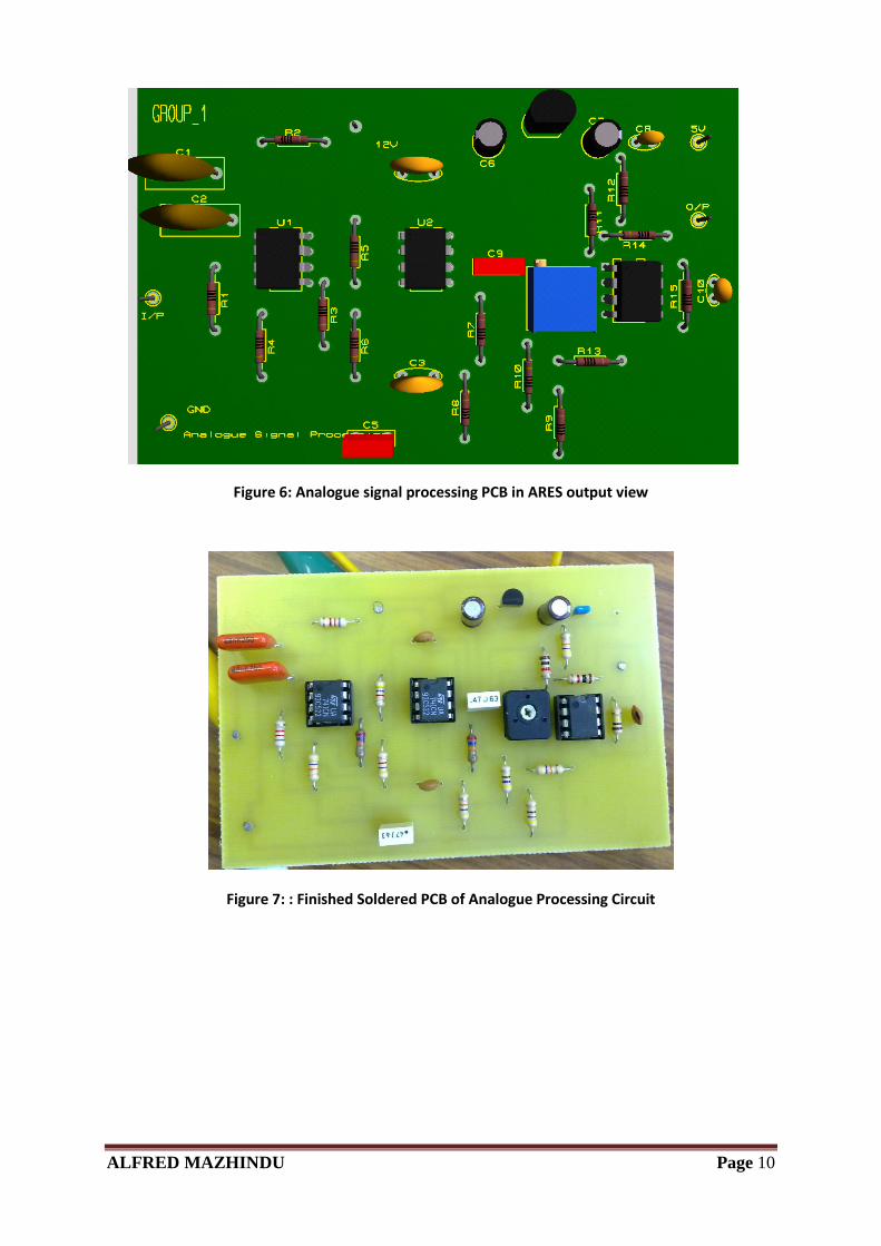
3. Designing the PCBs on Proteus ARES (Task 11)
After the PCB was made components were soldered on the PCB. The completed circuit
was then tested several time, double checked several times to make sure it functions
according. A functioning circuit was achieved and the square wave displayed on
oscilloscope. The following figures show stages of developing the Analogue Processing
Circuit from schematic, PCB, component soldering and testing.
Figure 5: Analogue signal processing PCB design (Second Stage)
3
2
6
74 1 5
U1
741
3
2
6
74 1 5
U2
741
VI3
VO1
GN
D2
U378L05
3
2
1
84
U4:A
TS372
56
7
84
U4:B
TS372
RV14k7
C1
68n
C2
68n
C36n8
C4
6n8
C5470n
C610uF
C710uF
C8100n
C9
470n
C10
4p7
R18k2
R2
8k2
R327k
R447k
R5
8k2
R6
8k2
R727k
R847k
R9470
R10470
R11
1k
R12
47k
R1347k
R14
1k
R15
100k
1
+12
PIN
1
DOPPLER SIGNAL
PIN1
GNDPIN
1
OUTPUTPIN
GROUP DESIGN PROJECT (FILTER AND COMPARATOR CIRCUIT)_GROUP 1
Group Members: A.Mazhindu, B. Motswetla, C. Potamialis, X. Gong and S. Chiweshe
ALFRED MAZHINDU Page 10
Figure 6: Analogue signal processing PCB in ARES output view
Figure 7: : Finished Soldered PCB of Analogue Processing Circuit

ALFRED MAZHINDU Page 11
Figure 8: Analogue Signal Processing PCB Testing and Measurement Displaying the square wave
Figure 9: Digital signal µProcessor Stage 1
The above circuit was designed with the help or assistance from Dr R Halliwell’s PCB basic
design from Blackboard. Then we improve the circuit to meet our requirements, testing the
circuit while on PC carried out by downloading the lcd_test.HEX to the chip PIC16F88, and
then the display shows the program code configured “Hello World” with a delay time.
RA7/OSC1/CLKIN16
RB0/INT/CCP16
RB1/SDI/SDA7
RB2/SDO/RX/DT8
RB3/CCP19
RB4/SCK/SCL10
RB5/SS/TX/CK11
RB6/AN5/T1OSO/T1CKI12
RB7/AN6/T1OSI13
RA0/AN017
RA1/AN118
RA2/AN2/CVREF/VREF-1
RA3/AN3/C1OUT/VREF+2
RA4/AN4/T0CKI/C2OUT3
RA6/OSC2/CLKOUT15
RA5/MCLR4
U1
PIC16F88
D7
14
D6
13
D5
12
D4
11
D3
10
D2
9D
18
D0
7
E6
RW
5R
S4
VS
S1
VD
D2
VE
E3
LCD1LM016L
VDD
RV1POT
C1
1nF
C2
1nF
X1CRYSTAL
R110k
VDD
+5V
GND
GND
SW1SW-ROT-3
+SP
PIN
+MCLR
PIN
SP2
PIN
I/PPIN
-MCLR
PIN
OFF
PINSP1
PIN
R510k
R710k
R610k
R1010k
R210k
R910k
1
2
3
4
5
6
7
8
J3
CONN-SIL8
AM FM
+
-
+LED
PIN
-LED
PIN
PCB_PIC16F88_DOPPLER RADAR CONTROL CIRCUIT DIGRAM
GROUP_1 GROUP DESIGN PROJECT
Group Members: A.Mazhindu, B. Motswetla, C. Potamialis, X. Gong and S. Chiweshe
-LEDPIN
+LEDPIN
-SWPIN
+ SWPIN

ALFRED MAZHINDU Page 12
4 Order the PCB and the µprocessor (Task 12)
Figure 10: PCB Design of Doppler Radar Control uProcessor Unit Stage 2
Figure 11: Doppler Radar Control uProcessor Unit on ARES output view

ALFRED MAZHINDU Page 13
Figure 12: The Finished uProcessor PCB soldered
Tasks Completed
Most of the tasks that were allocated to me have been completed. Includes the Drawing
of the block Diagram (Task 5), Assembling the signal processing circuit on the
breadboard (Task 9), Designing the circuit in the Proteus ISIS (Task 10), Designing the
PCB on Proteus ARES (Task 11), Order the PCB and the µProcessor (Task 12),
Assemble PCB circuit (Task 16), ordering the PCBs’ and also drilling of the holes on
the PCB.
Tasks Residual
The radar motion detector system we are building is made of related blocks needs to be a
contained unit. It will require all sub-systems to be housed in a case, which is portable. The
power supply needs to be 12 volts supplied from the battery. The identified 12 volts battery is
a bit heavy and large and may require a better-quality box. Our intentions are to improve on
the system components. Otherwise we may have to use 10 of the most common 1.2V
batteries in a holder.
Benson has researched the appropriate size of the box (casing) and also taking into account
the material used in the box and the ability to attach the switches to the box. The Push-to-
make switches, speed selector switch and LEDs will be outside the case.
Chris and Simba have finished program code and hopefully Benson and Glen will have
sufficient time to assemble the whole unit. Therefore all members shall assist in assembling.
Now at this stage of the design, most of the group budget will be towards, the stand and the
required switches.

ALFRED MAZHINDU Page 14
CONCLUSION The tasks needs attention, though allocated tasks are almost done, I will be concentrating on
connecting the PCB circuit, LCD and programmed PIC and assemble the whole device
together with the assistance from colleagues. The device case has been ordered and we are
waiting for the delivery.
REFERENCES Halliwell, R. Dr (2009) PCB_Basic_Design, [University of Bradford], Available: Online
2010-1 SEM2 GROUP DESIGN PROJECT (ENG2037D_2010-1_SEM2_A) [16 February
2011]
Clarke, R.W. Dr (1995) GDP Lab Handbook 1011 Analogue processing circuit, [University
of Bradford], Available: Online 2010-1 SEM2 GROUP DESIGN PROJECT
(ENG2037D_2010-1_SEM2_A) > MODULE MATERIAL [24 JANUARY 2011]
APPENDICES Functional Requirements Specification
This organisation has been sub-contracted to SESAME Enterprises Inc., which seems to have
found a market to develop a range of motion detector systems. This project therefore involves
the development of a radar motion detector unit which can be re-programmed to implement
the range of detection functions required. In order to meet the demand, this group came up
with a block diagram as shown below, as a step forward into solving the problem. The group
will therefore work towards achieving a working system by building each of the sub-systems
below and finally putting them together for a working system. The µprocessor and LCD will
be programmed.
Radar motion detector:
Measuring velocity moving object
PIC16 µprocessor
Detection range >20m
Readout range 10mph – 150mph with accuracy 1mph
Sampling time < 500ms
“switch” system
Hand-held system
Internal power supply and LCD Display
ALFRED MAZHINDU Page 15
Table 1: Project Plan - Task Allocation
Task Objective Start Date Duration
(days)
1 Group Project Introduction 26-JAN 3
2 Researching more information about Doppler
radars
01-FEB 5
3 Doppler effect labs 02-FEB 2
4 Calculation of frequency range and antenna gain 09-FEB 4
5 Drawing the block Diagram 04-FEB 2
6 FRS and Project Plan 28-JAN 5
7 Calculating resistors and capacitors values for
filters
09-FEB 2
8 Order capacitors resistors and op-amp 08-FEB 1
9 Assembling the signal processing circuit on the
breadboard
11-FEB 3
10 Designing the circuit in the Proteus ISIS 04-FEB 2
11 Designing the PCB on Proteus ARES 11-FEB 2
12 Order the PCB and the Microprocessor 22-FEB 1
13 Program microprocessor 11-FEB 7
14 Design antenna and calculate angles 15-FEB 3
15 Assemble the horn Antenna 16-FEB 4
16 Assemble PCB circuit 02-MAR 2
17 Design PCB for Microprocessor 23-FEB 3
18 Assemble PCB for Microprocessor 01-MAR 2
19 Connect both PCB's and testing 02-MAR 2
20 Design the radar structure outfit 04-MAR 3
21 Assemble the Radar device 08-MAR 4
22 Design and assemble the Power supply 09-MAR 5
23 Testing of the Device 15-MAR 5
24 Writing the group report ONGOING 4
Group Leader:
Team facilitator:
Group Secretary:

ALFRED MAZHINDU Page 16
Calculations for the gain
The following are the calculations of the gain and the frequency
λ =
=
=0.028m
Data
Quantity Linear Units
10mW
1nW
10
784µ
R 20m
f 10.6GHz
c 3
Radar Equation
Where
R radius (range)
Wavelength
But
Let
Making subject of formula

ALFRED MAZHINDU Page 17
Frequency Calculations
The group decided to have the system display the speed in km/hr and mph but for the
calculation m/s will be used. The required range is 10mph to 150mph, so the miles were
converted to the required units as shown below:
Conversion of miles to km
⁄
⁄
Using the Doppler frequency equation:
An approximate value of 300 was used.
An approximate value of 5000 was used.
Calculations for the resistors of the Low-pass filter
Measurements were taken in the lab using the suggested values in the hand book and the
frequencies were found to be:
The measured results were not corresponding to the calculated values, so we had to fix the
capacitance to 6.8nF and change the value of the resistors of the low pass filter. The new
values of the resistors were calculated using the formula below.

ALFRED MAZHINDU Page 18
The new value was used and the filter was able to cut-off frequencies above 5 kHz and cut-
off steeply because of the attenuation of signals.
This is for a high cut-off frequency that will give us 156.5 mph maximum measured speed
which is slightly above the 150mph.
The decision is that, it is close to our required frequency 4,764 kHz. However we considered
tolerance and adopted these values.
Calculations for the Horn For our system the antenna gain of 18dB was chosen to estimate the corresponding values of
A, B and L from the chart given below.
Figure 13: Antenna Gain
Estimated values obtained:
Area of the horn at front

ALFRED MAZHINDU Page 19
Calculation of the height of H
10.36 cm
H
2.1cm
2x +2.1=10.36
X=4.13cm
H=√ (10.36² -4.13²)
=9.50cm
Calculation of the height of h
7.84cm
h
1cm
2x +1=7.84cm
X=3.42cm
h=√ (7.84²+3.42²)
= 7.05cm
Figure 14: Antenna Design
Figure 15: Antenna Design [2]
Figure 16: The Finished Designed Horn

ALFRED MAZHINDU Page 20
Program Code /* GROUP_1 Group Design Project 2011 */
/*Simbarashe Chiweshe, Alfred Mazhindu */
/*Benson Motswetla, Xiaoxi Gong */
/*Christos Potamialis */
#include "convert.c"
#pragma CLOCK_FREQ 3276800
char count = 0, ,tick;
int RBCount = 0, freq, speed, speed_max = 0;
int kph, kph_max = 0;
int mph, mph_max = 0;
const char* speed1 = "Max: " ;
char state = 0;
void interrupt()
{
if (intcon & 100b == 100b) // T0IF set?
{
clear_bit(intcon,T0IF);
count++;
if (count == 20) // sample @ 100ms
{
count = 0;
freq = RBCount;
RBCount = 0;
tick = 1;
}
}
if (intcon & 10b == 10b) // INTF set?
{
clear_bit(intcon, INTF);
RBCount++;
}
}
void showspeed (int target_speed)
{
lcd_print(speed1);
display_digits(target_speed);
}
void main()
{
_CONFIG1 = 0x3F2A;
_CONFIG2 = 0x3FFC;
set_bit(status, RP0);
option_reg = 10000011b; // need to set TMR0 scaler
= 16;
trisb = 00000001b;
trisa = 00011111b;
ansel = 0; // set all inputs to
be digital
clear_bit (status, RP0);
tmr0 = 0;
lcd_start();
delay_ms(255);
delay_ms(245);
lcd_cursor(0,0);
lcd_print("Welcome");
lcd_clear();
enable_interrupt(INTE);
enable_interrupt(T0IE);

ALFRED MAZHINDU Page 21
//enable_interrupt(GIE);
while(1)
{
if (tick)
{
// calculate speed from freq which is 1/10th of doppler
frequency*/
tick = 0;
// speed is in m/s
//speed = freq*28;
//speed = speed/20;
// calculate kph
kph = freq*36;
kph = kph/100;
kph = kph*28;
kph = kph/20;
if (kph > kph_max) kph_max = kph;
//calculate mph
mph = freq*36;
mph = mph/100;
mph = mph*28;
mph = mph/32;
if (mph > mph_max) mph_max = mph;
// check if newly calculated values ar egreater than
stored maximums
freq = 0;
}
if (porta & 100b == 100b) // A2 high
{
if (state == 0)
{
count = 0;
RBCount = 0;
enable_interrupt(GIE);
state = 1;
}
lcd_cursor(0,1);
showspeed(kph_max);
lcd_cursor(0,0);
display_digits(kph);
lcd_print(" kph ");
set_bit(portb,1);
}
else if (porta & 10000b == 10000b) // A4 high
{
if (state == 0)
{
count = 0;
RBCount = 0;
enable_interrupt(GIE);
state = 1;
}
lcd_cursor(0,1);
showspeed(mph_max);
lcd_cursor(0,0);
display_digits(mph);
lcd_print(" mph ");
set_bit(portb,1);
}
else
{

ALFRED MAZHINDU Page 22
if (state != 0)
{
disable_interrupt(GIE);
state = 0;
}
lcd_cursor(0,0);
lcd_print("Standby ");
lcd_cursor(0,1);
lcd_print(" ");
clear_bit(portb,1);
}
if (porta & 1b == 1b) //A0 high
{
//lcd_clear();
kph_max = 0;
mph_max = 0;
delay_ms(200);
}
}
}
List of Components (Parts and Values)
Resistors (All resistors are carbon film)
R1=R2=R5=R6=8.2Kohms
R3=27Komhs
R4=R8=R12=R13=47Kohms
R7=27Komhs
R9=R10=470ohms
R11=R14=1Kohms
R15=100Kohms
RV1=4.7Kohms(variable)
12 X 1Kohms(for the LCD circuit)
Capacitors
C1=C2=C3=C4=68nF Ceramic
C5=470nF Polyester
C6=C7=10uF Electrolytic
C8=100nF
C9=470nF Ceramic
C10=4.7pF
C1=C2=15pF Ceramic(for the LCD circuit)
Semi-conductors
LM741 x2(op-amp)
TS922(U4:A & U4:B)
78L05 Regulator
PIC16F88

ALFRED MAZHINDU Page 23
Miscellaneous
Small iron pins
Chip Socket-8 pin socket holder x 3
PCB x2
Housing
LCD display and socket
Push to make switch
Slide switch(3 pole)
Diodes
LED=Green(5mm diameter)
Bill of Materials (Comparison of suppliers)
The group was allocated with £40 and it was the responsibility of the Purchase Manager to
buy the required supplies and also making sure that the group got the best quality of products
at the cheapest price. The WG11 Stores had their set prices but if the Purchase manager could
find a cheaper supplier the WG11 Store would lower their prices. Caution was taken in
finding alternative suppliers we opted for reliable and well trusted suppliers such as Farnell,
RS Catalogue and Rapid.
Table 2: Order Sheet
Part WG11 Store Price(£) Alternative Source(£)
Resistors 0.01each 0.17each
PIC16F88 2.79 2.10
LCD 5.99 8.48
Xtal Oscillator 0.80 0.75
Switch(PTM) 0.73
Toggle Switch 0.69
Pins free Sold in bulk only
LM741 0.50 0.36
TS922 1.75 1.66
78L05 0.08 0.20
RV1 4k7 0.24 0.26
Capacitors