research activities on silicon radiation detectors at...
TRANSCRIPT

May 20, 20021st SIRAD Meeting/WorkshopG.-F. Dalla Betta
Research Activities on
Silicon Radiation Detectors at IRST
M. Boscardin, G.-F. Dalla Betta, P. Gregori, N. Zorzi
Centro per la Ricerca Scientifica e Tecnologica (ITC-irst),
Divisione Microsistemi
Via Sommarive 18, 38050 Povo (Trento)
http://www.itc.it

May 20, 20021st SIRAD Meeting/WorkshopG.-F. Dalla Betta
Microfabrication Facility 250sq.m class 10, 250sq.m class 100; 4 inch wafers
Equipment: Ion implanter;
11 furnaces ;
Mask Aligner;
Sputter metal deposition;
Dry etching: Al, SiO2, poly and Si3N4;
Dicing Saw and ball bonder.
Clean Room Staff: 4 researchers, 12 operators
Simulation and design tools: Tanner tools, SILVACO and ISE-TCAD
Testing Lab. : Manual probe station (Karl Suess PM8);
Automatic probe station (Electroglas 2001 CX) for double-sided detectors;
Parametric test system (HP4062UX, HP4145B, HP4280A, HP4192A, Keithley 2410)
Microelectronics at IRST

May 20, 20021st SIRAD Meeting/WorkshopG.-F. Dalla Betta
• Starting from 1994, ITC-IRST has been involved in the
development of silicon radiation detector technologies within an
R&D project supported by INFN.
• Currently, production and research activities on detectors are
carried on in parallel:
- Several hundreds of double-sided microstrip detectors are
being fabricated for the AMS2 and CERN/ALICE experiments
- Single-sided microstrip detectors with integrated, JFET-based
electronics and pixel detectors for X-ray imaging applications in
the medical field are being developed, in cooperation with INFN
Silicon Radiation Detectors (SRD) Project

May 20, 20021st SIRAD Meeting/WorkshopG.-F. Dalla Betta
Development of µstrip detector technologies
Double sided detectors with integratedpoly-Si bias resistors and coupling capacitors
n S i-su b s tra te-
p+
p+
p+
p+
n+
n+
S iO
T E O S 1
T E O S 2
p o ly -S i
m e ta l
o v e rg la ss
2
Layout of CMS-like detectors
Cross section of a double-sided detector

May 20, 20021st SIRAD Meeting/WorkshopG.-F. Dalla Betta
Telescope detector
Test structures
Telescope detector
a b
ALICE oriented µstrip detectors
ALICE detectora: width = 50 µmb: width = 30 µm
Double-sided, Area = 75x42 mm2 , AC-coupled, punch-through bias

May 20, 20021st SIRAD Meeting/WorkshopG.-F. Dalla Betta
Experimental results
Strip leakage current distribution Detector AC scan

May 20, 20021st SIRAD Meeting/WorkshopG.-F. Dalla Betta
ATLAS Pixel Detector prototypes
LAD
SMD
NOD
“moderated p-spray isolation”
pixel “n-on-n”
oxygen enriched substrate
n-
A specially tailored technology has been developed for the fabrication of ATLAS pixel detector prototypes on thin silicon wafers (250 µm).
May 20, 20021st SIRAD Meeting/WorkshopG.-F. Dalla Betta
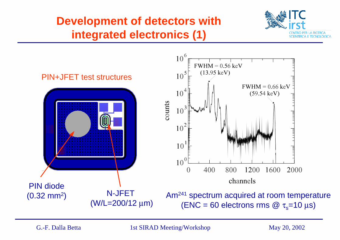
N-JFET (W/L=200/12 µm)
PIN diode(0.32 mm2) Am241 spectrum acquired at room temperature
(ENC = 60 electrons rms @ τs=10 µs)
Development of detectors with integrated electronics (1)
PIN+JFET test structures

May 20, 20021st SIRAD Meeting/WorkshopG.-F. Dalla Betta
PRIN Project with Univ. of Pisa, Pavia, Trieste, Bergamo.
Microstrip detector with JFET-based source-follower
Charge sensitive preamplifier
Development of detectors with integrated electronics (2)

May 20, 20021st SIRAD Meeting/WorkshopG.-F. Dalla Betta
�����������
���(���
���(���
���(���
���(���
��� ���� ����� ����� �����
'HSWK >XP@
&RQFHQWUDWLRQ>DW�FP
�@
V��
V��
V��
Optimization of oxygenation processes
Oxygen concentration profiles measured by SIMS (ITME, Poland) on IRST Si samples
Irradiation tests in progress with :
• Neutrons and protons at Legnaro (collaboration with INFN Padova)
• High energy electrons at Trieste (collaboration with INFN Trieste)

May 20, 20021st SIRAD Meeting/WorkshopG.-F. Dalla Betta
Studies of radiation damage from high energy electrons (Elettra, Trieste)
• Motivated by results from
BaBar microstrip detectors
• Test structures irradiated with
900 MeV electrons
• Both surface and bulk
radiation damage observed
• Substrate type-inversion
Increasing fluence

May 20, 20021st SIRAD Meeting/WorkshopG.-F. Dalla Betta
60Co γ irradiation of integrated JFETs
Noise spectral density of single JFET (triode, W/L=100/4), before and after irradiation with 60Co up to 750kRad
Equivalent Noise Charge of the monolithic preamplifier before and after exposure to γ-ray doses of 20kGy and 40 kGy

May 20, 20021st SIRAD Meeting/WorkshopG.-F. Dalla Betta
Neutron irradiation of multiguard termination structures (ENEA Frascati)
Φ=1x1012 cm-2
(1MeV eq.)
Standard multiguard termination All-p-type multiguard termination
Φ=1x1012 cm-2
(1MeV eq.)

May 20, 20021st SIRAD Meeting/WorkshopG.-F. Dalla Betta
• Silicon radiation detectors represent one of the main research
activities at ITC-IRST
• In the near future, the need for radiation damage tests is
foreseen for:
- ALICE microstrip detectors (low fluence)
- Microstrip detectors with integrated electronics
- Oxygenated silicon wafers
- All-p-type termination structures
- New detector structures (thin and 3D, CERN RDXX)
Conclusions