research article performances of an interleaved high step
TRANSCRIPT
Hindawi Publishing CorporationInternational Journal of PhotoenergyVolume 2013, Article ID 834510, 15 pageshttp://dx.doi.org/10.1155/2013/834510
Research ArticlePerformances of an Interleaved High Step-UpConverter with Different Soft-Switching Snubbers forPV Energy Conversion Applications
Sheng-Yu Tseng, Hung-Yuan Wang, and Chih-Yang Hsu
Department of Electrical Engineering, Chang-Gung University, 259 Wen-Hwa 1st Road, Kwei-shan, Taoyuan 33302, Taiwan
Correspondence should be addressed to Sheng-Yu Tseng; [email protected]
Received 5 July 2013; Revised 12 September 2013; Accepted 22 October 2013
Academic Editor: Wayne A. Anderson
Copyright © 2013 Sheng-Yu Tseng et al.This is an open access article distributed under the Creative CommonsAttribution License,which permits unrestricted use, distribution, and reproduction in any medium, provided the original work is properly cited.
This paper proposes an interleaved high step-up converter with different soft-switching snubbers for PV energy conversion appli-cations. For the high step-up converter, interleaved and coupled-inductor technologies are used to reduce output ripple current andincrease output power level. Simultaneously, two types of snubbers, a single-capacitor snubber and boost type snubber, areintroduced separately into the discussed converters for comparing their performances of conversion efficiency and switching losses.For drawing maximum power from the PV arrays, a perturbation-and-observation method realized with the microcontroller isadopted to achieve maximum power point tracking (MPPT) algorithm and power regulating scheme. Finally, two prototypes ofthe interleaved coupled-inductor boost converter with a single-capacitor snubber and with boost type snubber are implemented,respectively. The experimental results obtained are used to verify and compare the performances and feasibilities of the discussedconverters with different snubbers in PV conversion applications.The experimental results show that the proposed system is suitablefor PV energy conversion applications when the duty ratios of switches of the converter are less than 0.5.
1. Introduction
In recent years, in order to offer enough energy to maintainthe economic development of the world, one of the solutionsis the solar energy which is a totally inexhaustible and com-pletely clear energy source. However, due to the instabilityand intermittent characteristics of solar energy, photovoltaic(PV) power conversion systems with power converter andmaximum power tracking algorithms are needed to convertsolar energy into electrical energy and provide stable poweroutput. With the rapid growth of power electronics tech-niques, the conversion efficiency of PV power conversionsystem has been increased obviously [1, 2]. Recently, PVpower conversion systems are well recognized and widelyused in electric power conversion system, such as PV powergeneration for grid connection, PV vehicle constriction, bat-tery charger, water pumping, and satellite power conversionsystem.
To extract power from PV arrays, power converter is usedin PV power conversion systems. In order to obtain the
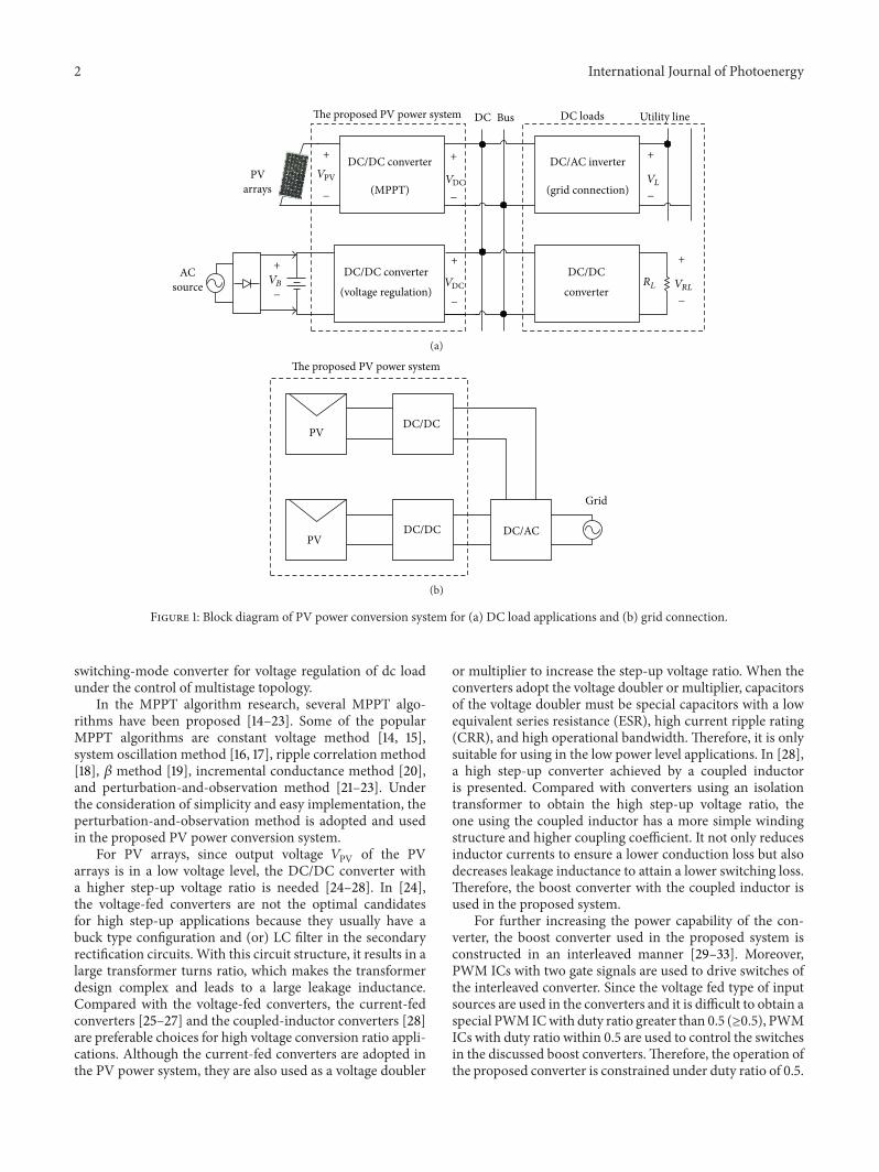
maximumpower fromPVarrays and thus increase utility rateof PV arrays, switching-mode converter must be operated atthe maximum power point (MPP) of PV arrays, resulting inits output voltage without keeping in the desired dc constantvoltage.Therefore, a switching-mode one with battery sourcein parallel is used for keeping the output voltage in the desireddc constant voltage, as shown in Figure 1(a). In Figure 1(a),dc voltages provided by the proposed PV power conversionsystem can be supplied to dc loads of dc/ac inverters forgrid-connected power conversion system [3–8] and dc/dcconverter for dc load [9–13]. In grid-connected power con-version system applications, control of power converters hasto be taken into consideration. In [4], three different controltopologies have been proposed according to the number ofpower processing stages. Since the multistage topology, asshown in Figure 1(b), possesses a better control performanceof each DC/DC converter, it is adopted in the proposedPV power conversion system. Therefore, the PV powerconversion system consists of a switching-mode converter formaximum power point tracking (MPPT) of PV arrays and a
2 International Journal of Photoenergy
DC/DC converter
(MPPT)
DC/AC inverter
(grid connection)
DC/DC converter
(voltage regulation)
DC/DC
converter
PVarrays
ACsource
The proposed PV power system DC Bus DC loads Utility line
VL
VB VRLRL
+
−
+
−
+
−
+
−
+
−
+
−
VDC
VDC
VPV
(a)
PVDC/DC
DC/ACDC/DCPV
Grid
The proposed PV power system
(b)
Figure 1: Block diagram of PV power conversion system for (a) DC load applications and (b) grid connection.
switching-mode converter for voltage regulation of dc loadunder the control of multistage topology.
In the MPPT algorithm research, several MPPT algo-rithms have been proposed [14–23]. Some of the popularMPPT algorithms are constant voltage method [14, 15],system oscillation method [16, 17], ripple correlation method[18], 𝛽 method [19], incremental conductance method [20],and perturbation-and-observation method [21–23]. Underthe consideration of simplicity and easy implementation, theperturbation-and-observation method is adopted and usedin the proposed PV power conversion system.
For PV arrays, since output voltage 𝑉PV of the PVarrays is in a low voltage level, the DC/DC converter witha higher step-up voltage ratio is needed [24–28]. In [24],the voltage-fed converters are not the optimal candidatesfor high step-up applications because they usually have abuck type configuration and (or) LC filter in the secondaryrectification circuits. With this circuit structure, it results in alarge transformer turns ratio, which makes the transformerdesign complex and leads to a large leakage inductance.Compared with the voltage-fed converters, the current-fedconverters [25–27] and the coupled-inductor converters [28]are preferable choices for high voltage conversion ratio appli-cations. Although the current-fed converters are adopted inthe PV power system, they are also used as a voltage doubler
or multiplier to increase the step-up voltage ratio. When theconverters adopt the voltage doubler or multiplier, capacitorsof the voltage doubler must be special capacitors with a lowequivalent series resistance (ESR), high current ripple rating(CRR), and high operational bandwidth. Therefore, it is onlysuitable for using in the low power level applications. In [28],a high step-up converter achieved by a coupled inductoris presented. Compared with converters using an isolationtransformer to obtain the high step-up voltage ratio, theone using the coupled inductor has a more simple windingstructure and higher coupling coefficient. It not only reducesinductor currents to ensure a lower conduction loss but alsodecreases leakage inductance to attain a lower switching loss.Therefore, the boost converter with the coupled inductor isused in the proposed system.
For further increasing the power capability of the con-verter, the boost converter used in the proposed system isconstructed in an interleaved manner [29–33]. Moreover,PWM ICs with two gate signals are used to drive switches ofthe interleaved converter. Since the voltage fed type of inputsources are used in the converters and it is difficult to obtain aspecial PWMICwith duty ratio greater than 0.5 (≥0.5), PWMICs with duty ratio within 0.5 are used to control the switchesin the discussed boost converters.Therefore, the operation ofthe proposed converter is constrained under duty ratio of 0.5.

International Journal of Photoenergy 3
When a coupled inductor boost converter is used in thePV power conversion system, the energy trapped in the leak-age inductor of coupled inductor not only increases voltagestresses but also induces switching lossless of switches in theconverter, significantly. In order to solve these problems, sev-eral methods have been proposed [34–36]. In [34], a resistor-capacitor-diode (R-C-D) snubber is used to alleviate voltagestresses of switches by dissipating the energy trapped in theleakage inductor through the resistor, reducing the conver-sion efficiency of the converter. Therefore, a passive losslesscircuit proposed in [35] is adopted to reduce voltage spikeacross switches. Its schematic diagram with the interleavedmanner is shown in Figure 2. Although converters with apassive lossless circuit can improve conversion efficiency,active switches are still operated in hard switching at turn-on transition. In [36], an active clamp circuit is introducedto achieve zero-voltage switching (ZVS) and increased itsconversion efficiency. However, the disadvantage of the activeclamp circuit is that it is difficult to implement soft-switchingfeatures at light load for the boost converter. In order tosolve this problem, a boost type snubber is inserted intothe active clamp boost converter with coupled inductor,as shown in Figure 3. It can improve conversion efficiencyof the boost converter at light load, significantly. Due to thecomplexity of circuit structures shown in Figures 2 and 3,they are, respectively, simplified by [37] and [38] and areshown in Figures 4(a) and 4(b). In this paper, performancecomparisons between the discussed converters with thesingle-capacitor snubber and with boost type snubber areproposed.
2. Control Algorithm ofthe Proposed Converter
When a switching-mode dc/dc converter is adopted as theirpower processor for extracting power from PV arrays andconverting the power into dc voltage supplied to dc loads, aproper powermanagement system formanaging the power isneeded in the PV power conversion system. In the following,the circuit topology of the proposed converter power conver-sion system, MPPT algorithm, and power management aredescribed.
2.1. Circuit Topology of the Proposed Converter. TheproposedPV power conversion system uses PV arrays as one of itspower sources. For increasing the utility rate of the PV arrays,the PV arrays have to be operated on their maximum power.Therefore, as shown in Figure 5, a PV power conversionsystem constructed of a switching-mode converter withPV array sources, a switching-mode converter with batterysource, and a controller is proposed. In the proposed PVpower system, the two dc/dc converters are realized by aninterleaved coupled-inductor boost converter with single-capacitor snubber shown in Figure 4(a). The one with PVarrays source uses MPPT control algorithm for extractingthe maximum power from PV arrays. The other with batterysource uses voltage regulation control method to regulatepowers between PV arrays and loads and to generate aconstant output voltage supplied to dc loads. As shown
in Figure 5, controller constructed by MPPT unit, powermanagement unit, and PWM IC unit is used to controlthe dc/dc converter with PV array source for determiningthe MPP of PV arrays by the perturbation-and-observationmethod described in [21–23].There are two signals generatedby the power management, control signals 𝑀
1and 𝑆
𝑃.
Control signal 𝑀1is used to regulate output powers of
switching-mode converter with MPPT control algorithm.Control signal 𝑆
𝑃is generated according to the relationships
between the maximum power 𝑃PV(max) of PV arrays andpower of load 𝑃
𝐿. Based on the control signal 𝑆
𝑃and the
output 𝑉𝑂, PWM IC unit generates control signal 𝑀
2with
voltage regulation control method for obtaining constantoutput voltage. Protections are considered and implementedby microcontroller. The protections include over-current,over-voltage, and over-temperature protections of the twoconverters and undercharge of battery. Therefore, the pro-posed PV power conversion system can be used to achievethe optimal utility rate of PV arrays.
2.2. Power Management. The power of PV arrays is suppliedto the load through the proposed interleaved boost converter.The power management of the proposed power conversionsystem is implemented by a microcontroller and is used toregulate the power of PV arrays and output power. Accordingto relationships among the powers of 𝑃PV, 𝑃𝑉𝐵, and 𝑃𝐿,operational modes of powermanagement can be divided into8 modes and are illustrated in Table 1. Power 𝑃PV is outputpower of switching-mode converter with PV arrays as itspower source, 𝑃
𝑉𝐵is that of switching-mode converter with
battery as its power source, and𝑃𝐿is power of load.Moreover,
“1” represents that the power is generated by switching-modeconverter or is required by load, while “0” represents thatthe power is not generated by switching-mode converter oris not required by load. According to the operational modesillustrated in Table 1, PV power conversion system is shutdown in operational modes of I, II, III, V, and VII. Therefore,operational modes IV, VI, and VIII are described as follows.
2.2.1. Operational Mode IV. In mode IV, the switching-modeconverter with battery is used to supply power to the load.Once the condition of 𝑃
𝐿> 𝑃𝑉𝐵(max) is reached or energy
stored in battery is completely discharged, the proposedconverter is shut down.
2.2.2. OperationalModeVI. InmodeVI, the switching-modeconverter with PV arrays as its power source is used to supplypower to load. When power of 𝑃PV(max) is equal to or greaterthan that of 𝑃
𝐿, power curve of PV arrays follows that of load.
Once 𝑃PV(max) < 𝑃𝐿, the proposed converter is shut down.
2.2.3. Operational VIII. When PV power conversion systemis operated in mode VIII, the interleaved boost convertersupplies power to load, as shown in Figure 6. During thisoperational mode, (𝑃PV(max) + 𝑃𝐵(max)) must be equal to orgreater than 𝑃
𝐿. If (𝑃PV(max) + 𝑃𝐵(max)) < 𝑃𝐿, the proposed
PV power conversion system is shut down. When (𝑃PV(max) +𝑃𝐵(max)) ≥ 𝑃𝐿, the operational condition can be further

4 International Journal of Photoenergy
Turn-off
Turn-off
A
D
RLCOVPV
+
−
+
−
L11 L12
L21 L22
M1 M2
D11
D21VO
snubber 1
snubber 2
E
B CS11
CS12 DS11
DS21
DS22
DS12
DS13
CS21
CS22
C
DS23
LS11
LS21
Figure 2: Schematic diagram of interleaved coupled-inductor boost converter with lossless turn-off snubber.
Activeclampcircuit
Activeclampcircuit Boost
type
RL
C1
C2
VPV
+
−
+
−
M1
M3
M2
M4
D1
D2
VOCO
DS2
DS1
1 : N
1 : NLM11
LM21
Lm21
Lm11
L1m
LN12
LN21
Lm12
Lm21
L2m L2S
L1S
LN11
LN21
2
1
Boost type snubber 1
snubber 2MS1 MS2
Figure 3: Schematic diagram of interleaved coupled-inductor boost converter with boost type snubber.
Table 1: Operational conditions of PV arrays for the proposed con-verter.
Operationalmodes
Power states Operational conditions of PVpower conversion system𝑃PV 𝑃𝑉𝐵 𝑃𝐿
I 0 0 0 ShutdownII 0 0 1 ShutdownIII 0 1 0 ShutdownIV 0 1 1 WorkingV 1 0 0 ShutdownVI 1 0 1 WorkingVII 1 1 0 ShutdownVIII 1 1 1 Working
divided into two cases: 𝑃PV(max) ≥ 𝑃𝐿 and 𝑃PV(max) < 𝑃𝐿. Inthe following, the two cases are briefly described.
(1) 𝑃𝑃𝑉(max) ≥ 𝑃𝐿 and 𝑃𝐵(max) < 𝑃𝐿. When 𝑃PV(max) ≥ 𝑃𝐿
and 𝑃𝐵(max) < 𝑃𝐿, the switching-mode converter with battery
source is shut down, causing the output power 𝑃PV of PVarrays to be equal to 𝑃
𝐿, as shown in Figure 6(a). Hence, the
switching-mode converter with PV arrays source is operatedin voltage regulationmode to supply the desired dc voltage toload.
(2) 𝑃𝑃𝑉(max) < 𝑃𝐿 and 𝑃𝐵(max) < 𝑃𝐿. When 𝑃PV(max) < 𝑃𝐿
and 𝑃𝐵(max) < 𝑃𝐿, the switching-mode converter with PV
array source is operated at the MPP of PV arrays to extractthe maximum power from the PV arrays. On the otherhand, the one with battery source is used to sustain thedesired dc voltage. Power curve for operational mode VIIIunder 𝑃PV(max) < 𝑃𝐿 and 𝑃𝐵(max) < 𝑃𝐿 is shown in Figure 6(b).From Figure 6(b), it can be seen that 𝑃
𝐿is the sum of 𝑃PV and
𝑃𝐵.

International Journal of Photoenergy 5
Single-capacitorsnubber RL
VPV
+
−
+
−
+
−
M1 M2
D1
D2
VO
VCS
CO
CS
1 : N
1 : N
Lk1
LK2
Lm22Lm21
Lm11
L22
Lm12
L12L11
L21
ID1 ID
ILm11
IL11 IL12I11
I21 IL22
ICS
ID2
ILm12
ILm22IDS2IDS1
IL21
ILm21
IO
(a)
Boost type snubberActive clamp circuit
RLVPV
+
+
−
−
+−
+
−
M1
M4
M3
M2
D1
D2
VO
VC1
VC2
CO
1 : N
1 : N
Lm12
L1m L1S
ID1
IDM3IL1S
IL2SIDSM
ILm11
IDM2IDM1
ILK21
ILK11
ILm21
IDM4
C1
C2
CM3
CM2
Lm11
LK11
LK21 LN21
Lm21
LN11 LN12
LN22
Lm22
L2m L2S
CM4
CM1
DM4
DM3
DM1 DM2
DB1
DB2
DS
MS
(b)
Figure 4: Schematic diagram of interleaved coupled-inductor boost converter (a) with a single-capacitor snubber and (b) with boost typesnubber.
3. Control Design of the Proposed PV PowerConversion System
As shown in Figure 7, controller of the proposed powerconversion system consists of twomajor units, the microcon-troller and the PWM IC units. The microcontroller is furtherdivided into theMPPT unit and the powermanagement unit.In the following, functions of each block will be describedbriefly.
3.1. The MPPT Unit. The MPPT unit uses the perturbation-and-observation method to track MPPT of PV arrays and todecide the maximum power 𝑃PV(max) of PV array, resulting inthe output power of 𝑃
𝑃for further power management.
3.2.The Power Management Unit. In the power managementunit, the maximum discharging current 𝐼
𝐵(max) of battery isset for obtaining the maximum battery discharging power𝑃𝐵(max) of 𝑉𝐵𝐼𝐵(max). Based on the output power of MPPT
unit 𝑃𝑃, the maximum battery discharging power, and the
load power 𝑃𝐿of 𝑉𝑂𝐼𝑂, comparator number 1 determines the
relationships between (𝑃PV + 𝑃𝐵(max)) and 𝑃𝐿. There are tworelationships to be discussed.
3.2.1. Case I: (𝑃PV + 𝑃𝐵(max)) ≥ 𝑃𝐿. When (𝑃PV + 𝑃𝐵(max)) ≥𝑃𝐿, control signal 𝑆
𝑃1of comparator number 1 is in the low
level, causing further comparison of 𝑃𝑃and 𝑃𝐿in comparator
number 2. If 𝑃𝑃≥ 𝑃𝐿, the low level output signal 𝑆
1of
comparator number 2 makes the power selector to set thepower 𝑃set to be equal to 𝑃
𝐿. Once 𝑃
𝑃< 𝑃𝐿, output signal 𝑆
1
of comparator number 2 becomes a high level and causes thepower selector to set the power 𝑃set to be equal to 𝑃𝑃.Then, inthe reference current block, the power 𝑃set and the referencevoltage 𝑉ref are used to calculate the reference current 𝐼
𝐶for
obtaining the current error value Δ𝐼𝐶(=𝐼𝐶−𝐼𝑂𝑃) with output
current of the proposed converter with PV array source, 𝐼𝑂𝑃,
in the current error amplifier.In the PWM generator of PV array, control signals 𝐺
1𝐴
and 𝐺2𝐴
are obtained by comparing current error value Δ𝐼𝐶
with triangular wave generated by the PWM generator of PVarrays. The control signals 𝐺
1𝐴and 𝐺
2𝐴are used to drive

6 International Journal of Photoenergy
PVarrays
DC/DC converter
DC/DC converter
(MPPT)
MPPTunit
Powermanagement
unit
PWM IC unit
(voltage regulation)
Microcontroller
PWM IC
Controller
RL
VPV
VPV
+
−
+
−
+
−
+
+
−
−M1
M1
M2
M2
VO
VO
VOVB
VO
CO
IO
IPVPPV
SP
Figure 5: Block diagram of the proposed PV power conversion system.
P
0
PL
PB
t
PPV(max)PPV
PB(max)
(a)
P
0t
PL
PB(max)
PB
PPV(max)
PPV(max) + PB(max)
PPV(max) + PB
(b)
Figure 6: Plot of power curves 𝑃PV, 𝑃𝐵, and 𝑃𝐿 (a) under 𝑃PV(max) ≥ 𝑃𝐿 and 𝑃𝐵(max) < 𝑃𝐿 and (b) under 𝑃PV(max) < 𝑃𝐿 and 𝑃𝐵(max) < 𝑃𝐿.
switches 𝑀1𝐴
and 𝑀2𝐴
of the proposed converter with PVarray source for controlling power flowed from PV arrays toload.
3.2.2. Case II: (𝑃PV + 𝑃𝐵(max)) < 𝑃𝐿. When (𝑃PV + 𝑃𝐵(max)) <𝑃𝐿, control signal 𝑆
𝑃1of comparator #1 is in the high level,
causing both of PWM generators of PV array and batteryto be shut down. The power management unit also includesfunctions of protection, which are over-voltage, over-current,under-voltage, and undercharge protections. As shown inFigure 7, there are six input signals to the protection con-troller,𝑉
𝑂(max),𝑉𝑂(min), 𝐼𝑂(max),𝑉𝐵(max), 𝐼𝑂,𝑉𝑂, and𝑉𝐵, where𝑉𝑂(max) and 𝑉𝑂(min) are maximum and minimum values of
output voltage, 𝐼𝑂(max) is maximum value of output current,
𝑉𝐵(min) is minimum value of battery voltage, 𝐼
𝑂is output
current, 𝑉𝑂is output voltage, and 𝑉
𝐵is voltage of battery.
When 𝑉𝑂≥ 𝑉𝑂(max), the proposed converter is operated in
over-voltage condition, causing the output signal 𝑆𝑃2to be in a
high level and shut down both of the PWMgenerators.More-over, conditions of 𝐼
𝑂≥ 𝐼𝑂(max) (over-current condition),
𝑉𝑂≤ 𝑉𝑂(min) (under-voltage condition), or 𝑉
𝐵≤ 𝑉𝐵(min)
(undercharge condition) also make signal 𝑆𝑃2
to be in a highlevel to shut down both of the PWM generators.
3.3. The PWM IC Unit. The proposed boost converter withbattery source uses lead-acid battery as its power source. Inorder to implement power balance among PV arrays, bat-tery, and load and sustain a constant output voltage, aPWM IC unit is adopted. This control unit includes voltageerror amplifier and PWM generator of battery. Based onthe output voltage 𝑉
𝑂and reference voltage 𝑉ref, the voltage
error amplifier determines the voltage error value Δ𝑉𝐶of

International Journal of Photoenergy 7
Perturb and
observe
method
(MPPT)
PWM generator of PV arrays
Current error amplifier
Current reference
Protectionjudgement
Calculate
Calculate
PWM generatorof battery
Voltage erroramplifier
MPPT unit
Microcontroller
Power selector
Power management unit
PWM IC unitController
The proposed boost converter with batteries
The proposed boost converter with PV arrays
RL
CO
CSA
CSB
VPV
VPV
+
−
+
−
+
−
M1AM2A
M2B
M1B
Lk1A L11A L12A
L21AL22A
Lm21A
Lm11A
Lm22A
LK2A
Lm12A
L11B
L21B L22B
L12B
Lm12BLm11B
Lm22BLm21B
1 : N
1 : N
1 : N
1 : N
D1A
D1B
D2A
D2B
VO
VO
VO
VO
G1A G2A
IPV
PsetPset
/VrefVref
Vref
SP2SP1
SP2 SP1
SP1
S1
ΔIc
Ic
IOP
IO
IO
IOB
IOP
IOP
IOP
IO
Comparator 2
Comparator 1
PP
PP
≥ PL
PB(max)
PLPP + PB(max) ≥ PL
VB
IB(max)
PL = VOIO
PB(max) = IB(max)VB VB
VB
VB
VO(max)VO(min)VB(min)IO(max)
ΔVC
G1BG2B
Lk1B
LK2B
Vref
Figure 7: Control diagram of the proposed power conversion system with the single-capacitor snubber for PV array applications.

8 International Journal of Photoenergy
ZVT at turn-offVDS
IDS
(VDS: 50V/div, IDS: 50A/div, time: 2𝜇s/div)
(a)
ZVT at turn-offVDS
IDS
(VDS: 50V/div, IDS: 50A/div, time: 2𝜇s/div)
(b)
Figure 8: Measured voltage 𝑉𝐷𝑆
and current 𝐼𝐷𝑆
waveforms of (a)switch 𝑀
1𝐵and (b) switch 𝑀
2𝐵under 50% of full load when the
proposed PV power conversion system with the single-capacitorsnubber.
ZVS at turn-on
VDS
IDS
ZVS at turn-on
VDVV S
IDI S
(VDS: 50V/div, IDS: 20A/div, time: 5𝜇s/div)
(a)
ZVS at turn-on
VDS
IDS
ZVS at turn-on
VDVV S
IDI S
(VDS: 50V/div, IDS: 20A/div, time: 5𝜇s/div)
(b)
Figure 9: Measured voltage 𝑉𝐷𝑆
and current 𝐼𝐷𝑆
waveforms of (a)switch 𝑀
1𝐵and (b) switch 𝑀
3𝐵of the proposed converter 50% of
full loadwhen the proposed PVpower conversion systemwith boosttype snubber.
VO
IO
(VO: 200V/div, IO: 2A/div, time: 100 ms/div)
(a)
VO
IO
(VO: 200V/div, IO: 2A/div, time: 100 ms/div)
VVVOVV
IOII
(b)
Figure 10: Output voltage𝑉𝑂and output current 𝐼
𝑂under step-load
changes between 0% and 100% of the full load of the active clampinterleaved boost converter (a) with the single-capacitor snubberand (b) with the boost type snubber.
(𝑉ref − 𝑉𝑂). The voltage error value Δ𝑉𝐶is then sent to
PWMgenerator of battery to be compared with triangle wavegenerated by PWM IC for obtaining PWM signals 𝐺
1𝐵and
𝐺2𝐵. Signals 𝐺
1𝐵and 𝐺
2𝐵are used to control switches 𝑀
1𝐵
and𝑀2𝐵
for regulating powers between PV arrays and load.Similarly, the PWM generator of battery can be shut downeither by signals 𝑆
𝑃1or 𝑆𝑃2.
4. Experimental Results
To verify performances of the proposed PVpower conversionsystem, dc/dc converters realized by the interleaved coupled-inductor boost converter with single-capacitor snubber andboost type snubber for generating dc voltage of 400V fordc load applications were implemented with the followingspecifications.
(A) The proposed boost converter with PV arrays is asfollows.
(i) Input voltage 𝑉PV: 34∼42V (PV arrays).(ii) Output voltage 𝑉
𝑂: 400Vdc.
(iii) Output maximum current 𝐼𝑂𝑃(max): 3 A.
(iv) Output maximum power 𝑃PV(max): 1.2 kW.
(B) The proposed boost converter with battery is as fol-lows.

International Journal of Photoenergy 9
0 t
tson tsoff
tri tritf� tf�
VDS VDS
IDB
IDPIDS IDS
(a)
0
Turn-onZVS
t
VDS VDS
IDB
IDP
IDSIDS
tritf�
tsoff
(b)
0 tTurn-offZVT
VDSVDS
IDB
IDPIDS
IDCIDB
tson
tri tf� TCC
(c)
Figure 11: Conceptual current and voltage waveforms of switch in the interleaved boost converter (a) with hard-switching circuit, (b) withboost type snubber, and (c) with single-capacitor snubber.
t
t
t
t
0
0
0
0
IL1IDP
IDP
IDP
IDP
IDB
IDB
IDB
IDB
IDB
IDPN + 1
IDPN + 1
IDBN + 1
IDBN + 1
DTS TS(1 − D)TSIL2
IDS1
IDS2
(a)
t
t
t
t
IL1IDP
IDP
IDP
IDP
IDB
IDB
IDB
IDB
IDPN + 1
DTS TS(1 − D)TSIL2
IDS1
IDS2
IDBN + 1
IDBN + 1
IDC
IDC
IDPN + 1
IDC
N + 1
IDC
N + 1
(0.5 − D)TS
TCC
0
0
0
0
IDB
(b)
Figure 12: Conceptual current waveforms of switches and inductors in the interleaved boost converter (a) with hard-switching circuit and(b) with single-capacitor snubber.
(i) Input voltage 𝑉𝐵: 44∼54Vdc (4 sets of 12 V bat-
tery connected in series).(ii) Output voltage 𝑉
𝑂: 400Vdc.
(iii) Output maximum current 𝐼𝑂𝐵(max): 3 A.
(iv) Output maximum power 𝑃𝐵(max): 1.2 kW.
According to designs and specifications of the proposedboost converters with the single-capacitor snubber, compo-nents of power stages in the proposed one are determined asfollows.
(i) Switches𝑀1𝐴,𝑀2𝐴,𝑀1𝐵, and𝑀
2𝐵: IRFP260N.
(ii) Diodes 𝐷1𝐴, 𝐷2𝐴, 𝐷1𝐵, and 𝐷
2𝐵: HFA08TB120 × 2
(connected in series).(iii) Coupled inductors 𝐿
𝑚11, 𝐿𝑚21
: 30 𝜇H.(iv) Leakage inductors of coupled inductors (𝐿
𝑚11, 𝐿𝑚12)
and (𝐿𝑚21, 𝐿𝑚22): 1.1 𝜇H.
(v) Cores of coupled inductors (𝐿𝑚11, 𝐿𝑚12) and (𝐿
𝑚21,
𝐿𝑚22): EE-55.
(vi) Turns ratio𝑁: 20.
Similarly, components of power stages in the proposedboost converters with boost type snubber are determined asfollows.
(i) Switches𝑀1𝐴∼𝑀𝑆𝐴: IRFP260N.
(ii) Switches𝑀1𝐵∼𝑀𝑆𝐵: IRFP260N.
(iii) Diodes 𝐷1𝐴, 𝐷2𝐴, 𝐷1𝐵, and 𝐷
2𝐵: HFA08TB120 × 2
(connected in series).(iv) Diodes 𝐷
𝐵1𝐴, 𝐷𝐵2𝐴
, 𝐷𝐵1𝐵
, 𝐷𝐵2𝐵
, and 𝐷𝑠:
HFA08TB120 × 2 (connected in series).(v) Coupled inductors 𝐿
𝑚11, 𝐿𝑚21
: 30 𝜇H.(vi) Leakage inductors of coupled inductors (𝐿
𝑚11, 𝐿𝑚12)
and (𝐿𝑚21, 𝐿𝑚22): 1.1 𝜇H.

10 International Journal of Photoenergy
50
60
70
80
90
100
(%)
(%)30 40 50 60 70 80 90 100
With the single-capacitor snubberWith hard-switching circuit
Boost type snubber
Figure 13: Comparison the efficiencies between the discussed inter-leaved boost converter with hard switching, with the single-capac-itor snubber, and with boost type snubber from light load to heavyload.
80ms
LecroyIPV
VPV
PPV
(VPV : 20V/div, IPV : 5A/div, PPV : 750W/div, time: 100ms/div)
8088080msmms
LecroyLLecroyIIPVPVII
VPVPVV
PPPPVPVPP
Figure 14: Measured voltage𝑉PV, current 𝐼PV, and power 𝑃PV wave-forms of the converter with PV arrays source and with the single-capacitor snubber under 𝑃PV(max) = 750W.
(vii) Cores of coupled inductor (𝐿𝑚11, 𝐿𝑚12) and (𝐿
𝑚21,
𝐿𝑚22): EE-55.
(viii) Turns ratio𝑁: 20.
(ix) Inductors 𝐿1𝑠, 𝐿2𝑠: 3 𝜇H.
(x) Cores of inductors 𝐿1𝑠, 𝐿2𝑠: DR28X12.
(xi) Capacitors 𝐶1𝐴, 𝐶2𝐴, 𝐶1𝐵, 𝐶2𝐵: 15 𝜇F.
To verify performances of the high step-up converterapplied to the PV power system, some of important compar-isons have beenmade and listed inTable 2. It can be seen fromTable 2 that the proposed boost converter with the single-capacitor snubber has less component counts, lower cost,and easier control circuit, while the proposed one with boosttype snubber has more component counts, higher cost, morecomplexity control circuit, and high conversion efficiency.They are suitable for middle or high power level applications.In addition, although the high step-up converters proposed
LecroyVO
IO
IOB
(VO: 200V/div, IOB: 2A/div, IO: 2A/div, time: 200𝜇s/div)
Figure 15: Measured voltage 𝑉𝑂, current 𝐼
𝑂𝐵, and 𝐼
𝑂waveforms of
the proposed PV power conversion system using the single-capaci-tor snubber operated in mode IV under 𝑃
𝐿= 350W.
LecroyVO
IO
IOP
LecroyLVOOVV
IOII
IOPPII
(VO: 200V/div, IOB: 2A/div, IO: 2A/div, time: 200𝜇s/div)
Figure 16: Measured voltage 𝑉𝑂, current 𝐼
𝑂𝑃, and 𝐼
𝑂waveforms of
the proposed PV power conversion system using the single-capaci-tor snubber operated in mode VI under 𝑃
𝐿= 600W.
in [25, 27] have higher conversion efficiency, they are onlyapplied to low or middle power level applications.
Moreover, hardware dimension of eachDC/DC converteris about 210 × 297mm. In order to verify the feasibility ofthe proposed boost converter with battery source, measuredvoltage 𝑉
𝐷𝑆and current 𝐼
𝐷𝑆waveforms of switches are
shown in Figures 8 and 9. Figure 8 shows those waveformsof switches 𝑀
1𝐵and 𝑀
2𝐵under 50% of full-load condition
when the proposed one adopts the single-capacitor snubber,while Figure 9 shows those waveforms of switches𝑀
1𝐵and
𝑀3𝐵
under 20% of full load condition when the proposedone uses boost type snubber. Experimental results reveal thatwhen the discussed boost converter with the single-capacitorsnubber is adopted, switches can be operated with zero-switching transition (ZVT) at turn-off transition. Switches ofthe discussed one with boost type snubber are operated withZVS at turn-on transition.
To make a fair comparison, the components of the boostconverter with hard-switching circuit, the single-capacitorsnubber, and boost type snubber are kept the same as possible.Figure 10 shows measured output voltage 𝑉
𝑂and current
𝐼𝑂
waveforms of the boost converter with three differentsnubbers under step-load changes between 0% and 100% offull load with repetitive rate of 0.5Hz and a duty ratio of 50%.From Figure 10, it can be observed that voltage regulations of

International Journal of Photoenergy 11
Table 2: Preliminary comparisons among the different high step-up converters for the PV power system.
Items for comparisonThe proposed boost
converter withsingle-capacitor snubber
The proposed boostconverter with boost type
snubber
The boost converterproposed in [25]
The high step-upconverter proposed in
[27]Key component counts
Active switch 2 5 4 4Passive switch 2 5 4 2Magnetic core 2 6 4 3Resonant/output capacitor 2 3 6 3
Seft-switching features
Main switches Turn on hard switchingturn off ZVT
Turn on ZVSturn off hard switching
Turn on ZVSturn off hard switching
Turn on ZVSturn off hard switching
Auxiliary switches Turn on ZVSturn off hard switching
Turn on ZVSturn off hard switching
Turn on ZVSturn off hard switching
Cost Lower High Middle LowDuty ratio limitation 𝐷 < 0.5 𝐷 < 0.5 𝐷 > 0.5 𝐷 > 0.5
Turns ratio of transformer 20 20 2.5 2.125Control complexity Middle (86%) High (90%) Higher (94.4%) Highest (96%)Conversion efficiency underfull load condition Simplicity Complexity Complexity Complexity
Power level application Middle power level High power level Lower power level Low power level
VO
IOB
IOP
LecroyVOVV
IOII BOO
IOPII
Lecroy
IO
(VO: 200V/div, IO: 2A/div, IOP: 1A/div, IOB: 1A/div, time: 200𝜇s/div)
Figure 17: Measured voltage𝑉𝑂, current 𝐼
𝑂𝐵, 𝐼𝑂𝑃, and 𝐼
𝑂waveforms
of the proposed PV power conversion system using the single-capacitor snubber operated in mode VIII under (𝑃
𝑃(max) +𝑃𝐵(max)) ≥𝑃𝐿and 𝑃PV(max) ≥ 𝑃𝐿.
output voltage𝑉𝑂of boost converter with the single-capacitor
snubber and boost type snubber are approximately the sameas the onewith hard-switching circuit. It reveals that the boostconverter with the single-capacitor snubber and boost typesnubber can yield a good dynamic performance.
According to the operational principles of the proposedconverters with the single-capacitor snubber and the boosttype snubber, switches of the proposed one with the single-capacitor snubber have ZVT features at turn-off transition,while those switches with the boost type snubber haveZVS features at turn-on transition. Their conceptual wave-forms are illustrated in Figures 11(b) and 11(c), respectively.Figures 12(a) and 12(b) show the current waveforms ofswitches and inductors in the interleaved coupled-inductor
(VO: 200V/div, IO: 2A/div, IOP: 1A/div, IOB: 1A/div, time: 100𝜇s/div)
VO
IOB
IOP
IO
VVOVV
IOII BOO
IOPII
IOII
Figure 18: Measured voltage𝑉𝑂, current 𝐼
𝑂𝐵, 𝐼𝑂𝑃, and 𝐼
𝑂waveforms
of the proposed PV power conversion system using the single-capacitor snubber operated in mode VIII under (𝑃
𝑃(max) +𝑃𝐵(max)) ≥𝑃𝐿and 𝑃PV(max) < 𝑃𝐿.
boost converter with hard-switching circuit and the single-capacitor snubber, respectively. From Figure 12(b), it canbe seen that when switch of one boost converter in theinterleaved boost converter is turned on, the diode current𝐼𝐷𝐶
of the other boost converter in the interleaved one flowsthrough the switch by the capacitor snubber. Therefore, theboost converter with the single-capacitor snubber will inducean extra turn-on switching loss. The key parameter values ofthe proposed interleaved boost converters with the single-capacitor snubber and with the boost type snubber underfull-load condition are listed in Tables 3 and 4, respectively.It can be found from Tables 3 and 4 that switching lossesof the proposed converter with the single-capacitor snubber,compared with those of the proposed one with the boost

12 International Journal of Photoenergy
Table 3: Parameter values of the boost converter with single-capacitor snubber under full-load condition.
Parameters Formulas Calculation values Practical values
𝐼𝐷𝐵
(𝑁 + 1)𝐼𝑂
2(1 − 𝐷)−𝑉PV𝐿1
𝐷𝑇𝑆 38.87A 39.5 A
𝐼𝐷𝑃
(𝑁 + 1)𝐼𝑂
2(1 − 𝐷)+𝑉PV𝐿1
𝐷𝑇𝑆 54.47A 56A
𝐼𝐷𝐶
(𝑁 + 1)𝐼𝑂
2(1 − 𝐷)+𝐷𝑉𝑂𝑇𝑆
𝐿1
−(𝑉𝑂− 𝑉PV)𝑇𝑆2𝐿1
12 A 63A
Switch stress 𝑉𝐷𝑆(max)
𝑁𝑉PV + 𝑉𝑂𝑁 + 1 53V 55V
Voltage across snubber capacitor 𝑉𝐶𝑆
(𝑉𝑂+ 𝑁𝑉PV) 1120V 1120V
Output diode stress (𝑉𝑂+ 𝑁𝑉PV) 1120V 1500V
Duty ratio𝐷𝑉𝑂− 𝑉PV
𝑁𝑉PV + 𝑉𝑂0.325 0.34
Snubber capacitor 𝐶𝑆
𝐶𝑆≥𝑡𝑠 off (𝑁𝑉PV + 𝑉𝑂)
(𝑁 + 1)(𝑉𝑂+ 𝑁𝑉PV)
2𝐼𝐷𝑃 1.16 nF 10 nF
𝑇𝐶𝐶
𝐶𝑆𝑉𝐷𝑆(max)
𝐼𝐷𝐵+ 𝐼𝐷𝐶
1.2 ns 9.9 ns
Switching loss of each switch at turn-on 𝑃𝑠 on
1
2𝑇𝑆
𝑉𝐷𝑆(max)(𝐼𝐷𝐵 + 𝐼𝐷𝐶)𝑡𝑠 on 5.86W 21.14W
Switching loss of each switch at turn-off 𝑃𝑠 off 0W 0W
Conduction loss of each switch 𝑃SC1
3𝑇𝑆
(𝐼𝐷𝑃
2 + 𝐼𝐷𝑃𝐼𝐷𝐵+ 𝐼𝐷𝐵
2)𝑅ds𝑡on 28.58W 30.31W
Conduction loss of diode 𝑃SCD 𝑉DF𝐼𝑂1(av) =1
2𝑉DF𝐼𝑂 7.2W 7.5W
Forward drop voltage 𝑉DF of output diode4.8V
(2.4V × 2)4.8V
(2.4V × 2)𝑡𝑠 on 87 ns 150 ns
𝑡𝑠 off
103 ns(𝑃𝑠 on calculation)
500 ns(𝐶𝑆calculation)
𝑉PV 36V 36V𝑉𝑂
400V 400V𝑇𝑆
20 𝜇s 20𝜇s𝐼𝑂
3A 3A𝑁 20 20𝑡on 𝐷𝑇
𝑆6.5 𝜇s 6.8𝜇s
𝑅ds 0.04Ω 0.04Ω
type sunbber, increase by 20∼30W. Comparison of efficien-cies among the discussed interleaved boost converters withdifferent types of snubbers is illustrated in Figure 13. It showsthat the boost converter with boost type snubber can yield thehighest conversion efficiency than that with single-capacitorsnubber from light load to heavy load.Conversion efficienciesof boost converters under full-load condition with boost typesnubber and single-capacitor are 86% and 90%, respectively.Since duty ratios of switches in two discussed PV powerconversion systems are less than 0.5, their turns ratios ofcoupled inductors have higher values. Therefore, a highercurrent flows through switches of the converter, resulting ina larger switching losses and conduction losses. Therefore,conversion efficiency of the converter in the two discussedPV power conversion systems can be further increased byreducing turns ratio of coupled inductor. Moreover, if the
conducted resistances𝑅𝐷𝑆(on) of switches in the converters are
reduced, those in the two discussed PVpower conversion sys-tems will be increased. That is, a lower conducted resistance𝑅𝐷𝑆(on) of switch can be chosen. In addition, two switches
connected in parallel can be used for reducing the conductedresistance. By doing so, conversion efficiency of the proposedconverter can be further increased by about 3∼5%.
Since the proposed boost converters with the single-capacitor and boost type snubbers use the same controlmethod, the measured results for MPPT and power man-agement should be the same. Therefore, only the measuredresults of the proposed one with the single-capacitor snubberare shown in this paper. From the measured waveforms ofvoltage 𝑉PV, current 𝐼PV, and power 𝑃PV under 𝑃PV(max) =750W shown in Figure 14, the tracking time of MPPTrealized by the proposed converter with PV arrays as its
International Journal of Photoenergy 13
Table 4: Parameter values of the boost converter with boost type snubber under full-load condition.
Parameters Formulas Calculationvalues Practical values
𝐼𝐷𝐵
(𝑁 + 1)𝐼𝑂
2(1 − 𝐷)−𝑉PV𝐿1
𝐷𝑇𝑆 38.87A 39A
𝐼𝐷𝑃
(𝑁 + 1)𝐼𝑂
2(1 − 𝐷)+𝑉PV𝐿1
𝐷𝑇𝑆 54.47A 56A
Switch stress 𝑉𝐷𝑆(max)
𝑁𝑉PV + 𝑉𝑂𝑁 + 1 53V 55V
Output diode stress (𝑉𝑂+ 𝑁𝑉PV) 1120V 1500V
Duty ratio D𝑉𝑂− 𝑉PV
𝑁𝑉PV + 𝑉𝑂0.325 0.34
Switching loss of each switch at turn-on 𝑃𝑠 on 0W 0W
Switching loss of each switch at turn-off 𝑃𝑠 off
1
2𝑇𝑆
𝑉𝐷𝑆(max)𝐼𝐷𝑃𝑡𝑠 off 7.43W 9.24W
Conduction loss of each switch 𝑃SC1
3𝑇𝑆
(𝐼𝐷𝑃
2 + 𝐼𝐷𝑃𝐼𝐷𝐵+ 𝐼𝐷𝐵
2)𝑅ds𝑡on 28.58W 30.31W
Conduction loss of diode 𝑃SCD 𝑉DF𝐼𝑂1(av) =1
2𝑉DF𝐼𝑂 7.2W 7.5W
Forward drop voltage 𝑉DF of output diode 4.8V (2.4 × 2) 4.8 V𝑡𝑠 on 87 ns 100 ns𝑡𝑠 off 103 ns 120 ns𝑉PV 36V 36V𝑉𝑂
400V 400V𝑇𝑆
20𝜇s 20𝜇s𝐼𝑂
3A 3A𝑁 20 20𝑡on 𝐷𝑇
𝑆6.5 𝜇s 6.8 𝜇s
𝑅ds 0.04Ω 0.04Ω
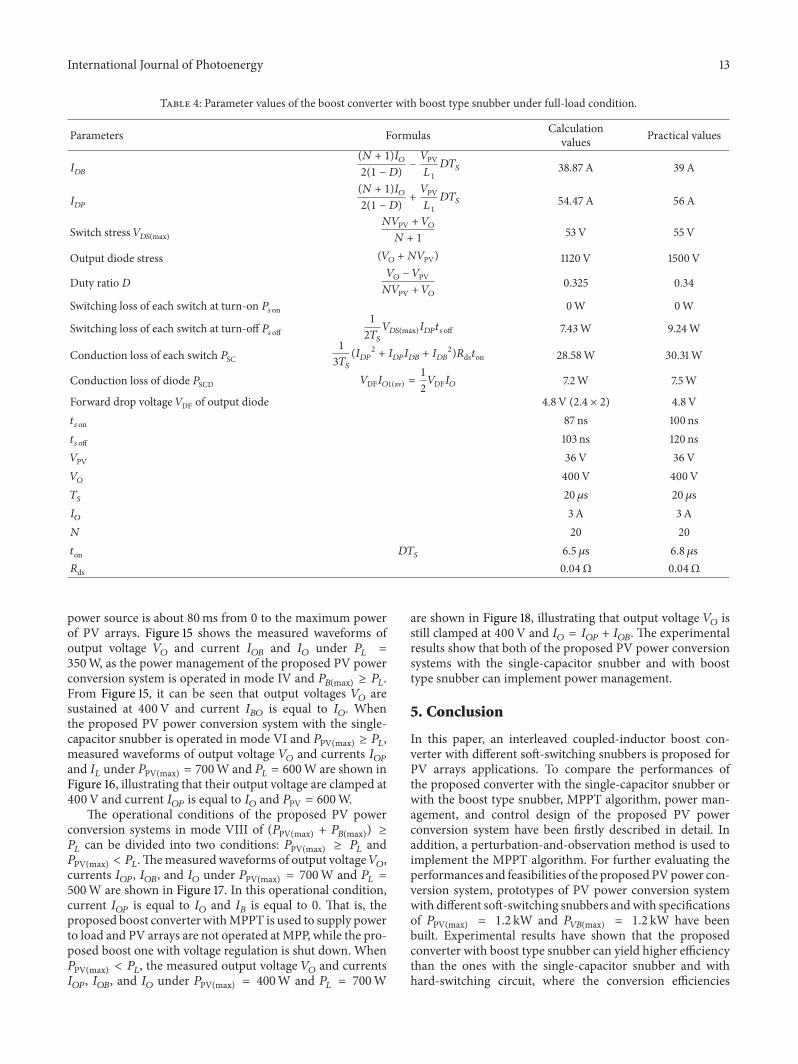
power source is about 80ms from 0 to the maximum powerof PV arrays. Figure 15 shows the measured waveforms ofoutput voltage 𝑉
𝑂and current 𝐼
𝑂𝐵and 𝐼
𝑂under 𝑃
𝐿=
350W, as the power management of the proposed PV powerconversion system is operated in mode IV and 𝑃
𝐵(max) ≥ 𝑃𝐿.From Figure 15, it can be seen that output voltages 𝑉
𝑂are
sustained at 400V and current 𝐼𝐵𝑂
is equal to 𝐼𝑂. When
the proposed PV power conversion system with the single-capacitor snubber is operated in mode VI and 𝑃PV(max) ≥ 𝑃𝐿,measured waveforms of output voltage 𝑉
𝑂and currents 𝐼
𝑂𝑃
and 𝐼𝐿under 𝑃PV(max) = 700Wand 𝑃
𝐿= 600Ware shown in
Figure 16, illustrating that their output voltage are clamped at400V and current 𝐼
𝑂𝑃is equal to 𝐼
𝑂and 𝑃PV = 600W.
The operational conditions of the proposed PV powerconversion systems in mode VIII of (𝑃PV(max) + 𝑃𝐵(max)) ≥𝑃𝐿can be divided into two conditions: 𝑃PV(max) ≥ 𝑃𝐿 and𝑃PV(max) < 𝑃𝐿.Themeasured waveforms of output voltage𝑉
𝑂,
currents 𝐼𝑂𝑃, 𝐼𝑂𝐵, and 𝐼
𝑂under 𝑃PV(max) = 700W and 𝑃
𝐿=
500W are shown in Figure 17. In this operational condition,current 𝐼
𝑂𝑃is equal to 𝐼
𝑂and 𝐼𝐵is equal to 0. That is, the
proposed boost converter withMPPT is used to supply powerto load and PV arrays are not operated at MPP, while the pro-posed boost one with voltage regulation is shut down. When𝑃PV(max) < 𝑃𝐿, the measured output voltage 𝑉
𝑂and currents
𝐼𝑂𝑃, 𝐼𝑂𝐵, and 𝐼
𝑂under 𝑃PV(max) = 400W and 𝑃
𝐿= 700W
are shown in Figure 18, illustrating that output voltage 𝑉𝑂is
still clamped at 400V and 𝐼𝑂= 𝐼𝑂𝑃+ 𝐼𝑂𝐵. The experimental
results show that both of the proposed PV power conversionsystems with the single-capacitor snubber and with boosttype snubber can implement power management.
5. Conclusion
In this paper, an interleaved coupled-inductor boost con-verter with different soft-switching snubbers is proposed forPV arrays applications. To compare the performances ofthe proposed converter with the single-capacitor snubber orwith the boost type snubber, MPPT algorithm, power man-agement, and control design of the proposed PV powerconversion system have been firstly described in detail. Inaddition, a perturbation-and-observation method is used toimplement the MPPT algorithm. For further evaluating theperformances and feasibilities of the proposed PVpower con-version system, prototypes of PV power conversion systemwith different soft-switching snubbers andwith specificationsof 𝑃PV(max) = 1.2 kW and 𝑃
𝑉𝐵(max) = 1.2 kW have beenbuilt. Experimental results have shown that the proposedconverter with boost type snubber can yield higher efficiencythan the ones with the single-capacitor snubber and withhard-switching circuit, where the conversion efficiencies

14 International Journal of Photoenergy
for converter with single-capacitor snubber and boost typesnubber are 86% and 90% under full load, respectively.Therefore, the proposed interleaved coupled-inductor boostconverter with the single-capacitor snubber is suitable for PVarrays applications with a lower cost, while the proposed onewith boost type snubber is applied to PV arrays for a higherconversion efficiency power conversion system.
References
[1] J. L. Duarte, J. A. A. Wijntjens, and J. Rozenboom, “Designinglight sources for solar-powered systems,” in Proceedings of the5th European Conference on Power Electronics and Applications,vol. 8, pp. 78–82, September 1993.
[2] U. Germann and H. G. Langer, “Low cost DC to AC converterfor photovoltaic power con-version in residential applications,”in Proceedings of the IEEE Power Electronics Specialist Confer-ence (PESC ’93), pp. 588–594, 1993.
[3] Y. Yu, Q. Zhang, B. Liang, X. Liu, and S. Cui, “Analysis ofa single-phase Z-Source inverter for battery discharging invehicle to grid applications,” Energies, vol. 4, no. 12, pp. 2224–2235, 2011.
[4] S. B. Kjaer, J. K. Pedersen, and F. Blaabjerg, “A review of single-phase grid-connected inverters for photovoltaicmodules,” IEEETransactions on Industry Applications, vol. 41, no. 5, pp. 1292–1306, 2005.
[5] P. J. Perez, G. Almonacid, J. Aguilera, and J. de la Casa, “RMScurrent of a photovoltaic generator in grid-connected PVsystems: definition and application,” International Journal ofPhotoenergy, vol. 2008, Article ID 356261, 7 pages, 2008.
[6] J. Yoo, B. Park, K. An et al., “Look-ahead energy managementof a grid-connected residential PV system with energy storageunder time-based rate programs,” Energies, vol. 5, article 4, pp.1116–1134, 2012.
[7] A. D. Gerlando, G. Foglia, M. F. Iacchetti, and R. Perini, “Anal-ysis and test of diode rectifier solutions in grid-connected windenergy conversion systems employing modular permanent-magnet synchronous generators,” IEEE Transactions on Indus-trial Electronics, vol. 59, no. 5, pp. 2135–2146, 2012.
[8] F. A. Ramirezand and M. A. Arjona, “Development of a grid-connected wind generationsys-temwith a modified PLL struc-ture,” IEEE Transactions on Sustainable Energy, vol. 3, no. 3, pp.474–481, 2012.
[9] T. M. van Breussegem andM. S. J. Steyaert, “Monolithic capaci-tive DC-DC converter with single boundary—multiphase con-trol and voltage domain stacking in 90nmCMOS,” IEEE Journalof Solid-State Circuits, vol. 46, no. 7, pp. 1715–1727, 2011.
[10] V. P. Galigekere and M. K. Kazimierczuk, “Analysis of PWMZ-source DC-DC converter in CCM for steady state,” IEEETransactions on Circuits and Systems I, vol. 59, no. 4, pp. 854–863, 2012.
[11] Z. Wang and H. Li, “A soft switching three-phase current-fedbidirectional DC-DC converter with high efficiency over a wideinput voltage range,” IEEE Transactions on Power Electronics,vol. 27, no. 2, pp. 669–684, 2012.
[12] H.-L. Do, “Improved ZVSDC-DC converter with a high voltagegain and a ripple-free input current,” IEEE Transactions onCircuits and Systems I, vol. 59, no. 4, pp. 846–853, 2012.
[13] W. Qian, H. Cha, F. Z. Peng, and L. M. Tolbert, “55-kW variable3X DC-DC converter for plug-in hybrid electric vehicles,” IEEE
Transactions on Power Electronics, vol. 27, no. 4, pp. 1668–1678,2012.
[14] S. L. Brunton, C. W. Rowley, S. R. Kulkarni, and C. Clarkson,“Maximum power point tracking for photovoltaic optimizationusing ripple-based extremum seeking control,” IEEE Transac-tions on Power Electronics, vol. 25, no. 10, pp. 2531–2540, 2010.
[15] V. Agarwal, R. K. Aggarwal, P. Patidar, and C. Patki, “A novelscheme for rapid tracking of maximum power point in windenergy generation systems,” IEEE Transactions on Energy Con-version, vol. 25, no. 1, pp. 228–236, 2010.
[16] M. Taherbaneh, A. H. Rezaie, H. Ghafoorifard, K. Rahimi, andM. B. Menhaj, “Maximizing output power of a solar panel viacombination of sun tracking and maximum power point track-ing by fuzzy controllers,” International Journal of Photoenergy,vol. 2010, Article ID 312580, 13 pages, 2010.
[17] X. Weidong and W. G. Dunford, “A modified adaptive hillclimbing MPPT method for photovoltaic power conversionsystems,” inProceedings of the 35thAnnual IEEE Power ElectronsSpecialists Conference, pp. 1957–1963, 2004.
[18] K. Kobayashi, H.Matsuo, and Y. Sekine, “An excellent operatingpoint tracker of the solar-cell power supply system,” IEEETransactions on Industrial Electronics, vol. 53, no. 2, pp. 495–499,2006.
[19] S. Subiyanto, A. Mohamed, and H. Shareef, “Hopfield neuralnetwork optimized fuzzy logic controller for maximum powerpoint tracking in a photovoltaic system,” International Journalof Photoenergy, vol. 2012, Article ID 798361, 13 pages, 2012.
[20] S. Jain and V. Agarwal, “A new algorithm for rapid tracking ofapproximate maximum power point in photovoltaic systems,”IEEE Power Electronics Letters, vol. 2, no. 1, pp. 16–19, 2004.
[21] H. S.-H. Chung, K. K. Tse, S. Y. R. Hui, C. M. Mok, and M.T. Ho, “A novel maximum power point tracking technique forsolar panels using a SEPIC or Cuk converter,” IEEE Transactionson Power Electronics, vol. 18, no. 3, pp. 717–724, 2003.
[22] M. T. Billy Ho, S. H. Henry Chung, and S. Y. R. Hui, “Anintegrated inverter with maximum power tracking for grid-connected PV systems,” in Proceedings of the 9th Annual IEEEApplied Power Electronics Conference and Exposition (APEC’04), vol. 3, pp. 1559–1565, 2004.
[23] D. Casadei, G. Grandi, and C. Rossi, “Single-phase single-stagephotovoltaic generation system based on a ripple correlationcontrol maximum power point tracking,” IEEE Transactions onEnergy Conversion, vol. 21, no. 2, pp. 562–568, 2006.
[24] Z. Liang, R. Guo, J. Li, and A. Q. Huang, “A high-efficiency PVmodule-integrated DC/DC converter for PV energy harvest inFREEDM systems,” IEEE Transactions on Power Electronics, vol.26, no. 3, pp. 897–909, 2011.
[25] H. Kim, C. Yoon, and S. Choi, “An improved current-fedZVS isolated boost converter for fuel cell applications,” IEEETransactions on Power Electronics, vol. 25, no. 9, pp. 2357–2364,2010.
[26] K. C. Tseng, C. C. Huang, and W. Y. Shin, “A high step-upconverter with a voltage multiplier module for a photovoltaicsystem,” IEEE Transactions on Power Electronics, vol. 28, no. 66,pp. 3047–3057, 2013.
[27] J.-M. Kwon and B.-H. Kwon, “High step-up active-clamp con-verter with input-current doubler and output-voltage doublerfor fuel cell power systems,” IEEE Transactions on Power Elec-tronics, vol. 24, no. 1, pp. 108–115, 2009.
[28] Y. Zhao, W. Li, Y. Deng, and X. He, “Analysis, design, andexperimentation of an isolated ZVT boost converter with

International Journal of Photoenergy 15
coupled inductors,” IEEE Transactions on Power Electronics, vol.26, no. 2, pp. 541–550, 2011.
[29] F. Yang, X. Ruan, Y. Yang, and Y. Zhihong, “Interleaved criticalcurrent mode boost PFC converter with coupled inductor,”IEEE Transactions on Power Electronics, vol. 26, no. 9, pp. 2404–2413, 2011.
[30] S. Dwari and L. Parsa, “An efficient high-step-up interleavedDC-DC converter with a common active clamp,” IEEE Trans-actions on Power Electronics, vol. 26, no. 1, pp. 66–78, 2011.
[31] O. Hegazy, J. V. Mierloand, and P. Lataire, “Analysis, modeling,and implementation of amulti-device interleaved DC/DC con-verter for fuelcell hybrid electric vehicles,” IEEE Transactions onPower Electronics, vol. 27, no. 11, pp. 4445–5558, 2012.
[32] W. Li, Y. Zhao, J. Wu, and X. He, “Interleaved high step-upconverter with winding-cross-coupled inductors and voltagemultiplier cells,” IEEE Transactions on Power Electronics, vol. 27,no. 1, pp. 133–143, 2012.
[33] L. Weichen, X. Xiang, L. Wuhua, and X. He, “Interleaved highstep-up ZVT converter with built-in transformer voltage dou-bler cell for distributed PV generation system,” IEEE Transac-tions on Power Electronics, vol. 28, no. 1, pp. 300–313, 2013.
[34] M. Peipei, C. Henglin, S. Zheng, W. Xinke, and Q. Zhaoming,“Optimal design for the damping resistor in RCD-R snubberto suppress common-mode noise,” in Proceedings of the 25thAnnual IEEE Applied Power Electronics Conference and Expo-sition (APEC ’10), pp. 691–695, 2010.
[35] R. T. H. Li, H. S.-H. Henry, A. K. T. Chung, and A .K. T. Sung,“Passive lossless snubber for boost PFC with minimum voltageand current stress,” IEEE Transactions on Power Electronics, vol.25, no. 3, pp. 602–613, 2010.
[36] B. Kim,H.-J. Ju, K.-C. Ko, and E. Hotta, “Active clamping circuitto suppress switching stress on a MOS-gate-structure-basedpower semiconductor for pulsed-power applications,” IEEETransactions on Plasma Science, vol. 39, no. 8, pp. 1736–1742,2011.
[37] S. Y. Tseng, J. Z. Shiang, and Y. H. Su, “A single-capacitorturn-off snubber for interleaved boost converter with coupledinductor,” in Proceedings of the 7th International Conference onPower Electronics and Drive Systems (PEDS ’07), pp. 202–208,2007.
[38] S. Y. Tseng, C. L. Ou, S. T. Peng, and J. D. Lee, “Interleavedcoupled-inductor boost converter with boost type snubber forPV system,” in Proceedings of the IEEE Energy Conversion Con-gress and Exposition (ECCE ’09), pp. 1860–1867, 2009.

Submit your manuscripts athttp://www.hindawi.com
Hindawi Publishing Corporationhttp://www.hindawi.com Volume 2014
Inorganic ChemistryInternational Journal of
Hindawi Publishing Corporation http://www.hindawi.com Volume 2014
International Journal ofPhotoenergy
Hindawi Publishing Corporationhttp://www.hindawi.com Volume 2014
Carbohydrate Chemistry
International Journal of
Hindawi Publishing Corporationhttp://www.hindawi.com Volume 2014
Journal of
Chemistry
Hindawi Publishing Corporationhttp://www.hindawi.com Volume 2014
Advances in
Physical Chemistry
Hindawi Publishing Corporationhttp://www.hindawi.com
Analytical Methods in Chemistry
Journal of
Volume 2014
Bioinorganic Chemistry and ApplicationsHindawi Publishing Corporationhttp://www.hindawi.com Volume 2014
SpectroscopyInternational Journal of
Hindawi Publishing Corporationhttp://www.hindawi.com Volume 2014
The Scientific World JournalHindawi Publishing Corporation http://www.hindawi.com Volume 2014
Medicinal ChemistryInternational Journal of
Hindawi Publishing Corporationhttp://www.hindawi.com Volume 2014
Chromatography Research International
Hindawi Publishing Corporationhttp://www.hindawi.com Volume 2014
Applied ChemistryJournal of
Hindawi Publishing Corporationhttp://www.hindawi.com Volume 2014
Hindawi Publishing Corporationhttp://www.hindawi.com Volume 2014
Theoretical ChemistryJournal of
Hindawi Publishing Corporationhttp://www.hindawi.com Volume 2014
Journal of
Spectroscopy
Analytical ChemistryInternational Journal of
Hindawi Publishing Corporationhttp://www.hindawi.com Volume 2014
Journal of
Hindawi Publishing Corporationhttp://www.hindawi.com Volume 2014
Quantum Chemistry
Hindawi Publishing Corporationhttp://www.hindawi.com Volume 2014
Organic Chemistry International
ElectrochemistryInternational Journal of
Hindawi Publishing Corporation http://www.hindawi.com Volume 2014
Hindawi Publishing Corporationhttp://www.hindawi.com Volume 2014
CatalystsJournal of