resistance switching memories are memristors - springer · pdf fileresistance switching...
TRANSCRIPT

Appl Phys A (2011) 102: 765–783DOI 10.1007/s00339-011-6264-9
Resistance switching memories are memristors
Leon Chua
Received: 17 November 2010 / Accepted: 22 December 2010 / Published online: 28 January 2011© The Author(s) 2011. This article is published with open access at Springerlink.com
Abstract All 2-terminal non-volatile memory devices basedon resistance switching are memristors, regardless of the de-vice material and physical operating mechanisms. They allexhibit a distinctive “fingerprint” characterized by a pinchedhysteresis loop confined to the first and the third quadrantsof the v–i plane whose contour shape in general changeswith both the amplitude and frequency of any periodic “sine-wave-like” input voltage source, or current source. In par-ticular, the pinched hysteresis loop shrinks and tends to astraight line as frequency increases. Though numerous ex-amples of voltage vs. current pinched hysteresis loops havebeen published in many unrelated fields, such as biology,chemistry, physics, etc., and observed from many unrelatedphenomena, such as gas discharge arcs, mercury lamps,power conversion devices, earthquake conductance varia-tions, etc., we restrict our examples in this tutorial to solid-state and/or nano devices where copious examples of pub-lished pinched hysteresis loops abound. In particular, wesampled arbitrarily, one example from each year betweenthe years 2000 and 2010, to demonstrate that the memristoris a device that does not depend on any particular mater-ial, or physical mechanism. For example, we have shownthat spin-transfer magnetic tunnel junctions are examples ofmemristors. We have also demonstrated that both bipolarand unipolar resistance switching devices are memristors.
The goal of this tutorial is to introduce some fundamen-tal circuit-theoretic concepts and properties of the memristorthat are relevant to the analysis and design of non-volatilenano memories where binary bits are stored as resistances
L. Chua (�)Berkeley Department of EECS, University of California,Berkeley, CA 94720, USAe-mail: [email protected]: +1-510-6438869
manifested by the memristor’s continuum of equilibriumstates. Simple pedagogical examples will be used to illus-trate, clarify, and demystify various misconceptions amongthe uninitiated.
1 Pinched hysteresis loops
The memristor [1] is a 2-terminal circuit element charac-terized by a constitutive relation between two mathematicalvariables q and ϕ representing the time integral of the ele-ment’s current i(t), and voltage v(t); namely,
q(t)�=
∫ t
−∞i(τ ) dτ (1)
ϕ(t)�=
∫ t
−∞v(τ) dτ (2)
It is important to stress that “q” and “ϕ” are defined math-ematically and need not have any physical interpretations.Nevertheless, we call q the charge and ϕ the flux of thememristor since (1) and (2) coincide with the formula relat-ing charge to current, and flux to voltage, respectively. Wesay the memristor is charge-controlled, or flux-controlled, ifits constitutive relation can be expressed by
ϕ = ϕ̂(q) (3)
or
q = q̂(ϕ) (4)
respectively, where ϕ̂(q) and q̂(ϕ) are continuous andpiecewise-differentiable functions1 with bounded slopes.
1A function is piecewise-differentiable if its derivative is uniquely de-fined everywhere except possibly at isolated points.

766 L. Chua
Differentiating (3) and (4) with respect to time t , we ob-tain
v = dϕ
dt= dϕ̂(q)
dq
dq
dt= R(q)i (5)
where
R(q)�= dϕ̂(q)
dq(6)
is called the memristance2 at q , and has the unit of Ohms (�),and
i = dq
dt= dq̂(ϕ)
dϕ
dϕ
dt= G(ϕ)v (7)
where
G(ϕ)�= dq̂(ϕ)
dϕ(8)
is called the memductance at ϕ, and has the unit of Siemens(S). Observe that (5) and (6) can be interpreted as Ohm’s lawexcept that the resistance R(q) at any time t = t0 dependson the entire past history of i(t) from t = −∞ to t = t0.Similarly the memductance G(ϕ) in (8) depends on the en-tire past history of v(t) from t = −∞ to t = t0. It followsfrom (5) that the charge-controlled memristor defined in (3)is equivalent to the charge-dependent Ohm’s law
v = R(q)i (9)
where R(q) is just the slope of the curve ϕ = ϕ̂(q) at q . Toshow that (3) and (5) are equivalent representations, we canrecover (3) by integrating both sides of (5) with respect to t :
ϕ�=
∫ t
−∞v(τ) dτ =
∫ t
−∞R
(q(τ)
)i(τ ) dτ
=∫ t
−∞R
(q(τ)
)dq(τ)
dτdτ
=∫ q(t)
q(−∞)
R(q(τ)
)dq(τ)
=∫ q(t)
q(−∞)
R(q) dq
= ϕ̂(q) (10)
It follows from (10) that
ϕ̂(q) =∫
R(q)dq (11)
2Just as memristor is an acronym for memory resistor, memristanceis an acronym for memory resistance. Similarly memductance is anacronym for memory conductance.
Similarly, a flux-controlled memristor is equivalent to theflux-dependent Ohm’s law
i = G(ϕ)v (12)
where
q̂(ϕ) =∫ ϕ(t)
ϕ(−∞)
G(ϕ)dϕ (13)
Example 1 Consider the charge-controlled memristor shownin Fig. 1(a) along with the memristor symbol in the upperleft corner. The memristor constitutive relation, shown inred, is described analytically by a cubic polynomial
ϕ = q + 1
3q3 (14)
Let us apply a sinusoidal current source (blue sine wavein Fig. 1(c)) defined by
{i(t) = A sinωt, t ≥ 0
= 0, t < 0(15)
across this memristor, as shown in Fig. 1(c) for A = 1 andω = 1. To determine the corresponding voltage responsev(t) from the constitutive relation (14), we must calculatefirst the corresponding charge (shown in red in Fig. 1(c)).Assuming the initial charge q0 = q(0) = 0, we obtain uponintegrating (15) the following equation for q(t):
q(t) =∫ t
0A sin(ωτ)dτ = A
ω[1 − cosωt], t ≥ 0 (16)
Substituting (16) into (14), we obtain the corresponding flux(shown in magenta in Fig. 1(d))
ϕ(t) = A
ω(1 − cosωt)
[1 + 1
3
(A2
ω2
)(1 − cosωt)2
](17)
Differentiating (17) with respect to t , we obtain
v(t) = A
[1 + A2
ω2(1 − cosωt)2
]sinωt (18)
Plotting the loci3 of (i(t), v(t)) in the v–i plane, via (15)and (18), we obtain the pinched hysteresis loop shown inFig. 1(b) for A = 1 and ω = 1. The hysteresis occurs be-cause the maxima and minima of the sinusoidal input currenti(t) in Fig. 1(c) do not occur at the same time as the corre-sponding memristor voltage v(t) in Fig. 1(d). The pinchingat the origin in Fig. 1(b) occurs because both i(t) and v(t)
become zero at the same time. To show that the hysteresis
3Also known as a Lissajous figure.
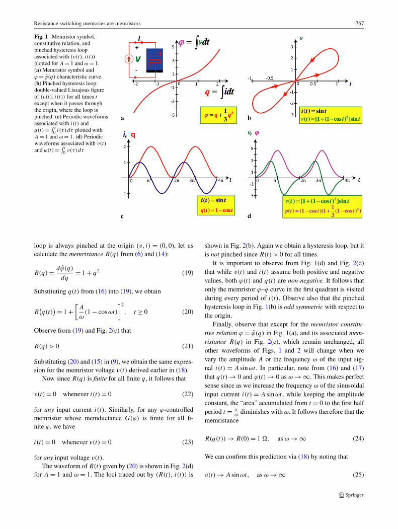
Resistance switching memories are memristors 767
Fig. 1 Memristor symbol,constitutive relation, andpinched hysteresis loopassociated with (v(t), i(t))
plotted for A = 1 and ω = 1.(a) Memristor symbol andϕ = ϕ̂(q) characteristic curve.(b) Pinched hysteresis loop:double-valued Lissajous figureof (v(t), i(t)) for all times t
except when it passes throughthe origin, where the loop ispinched. (c) Periodic waveformsassociated with i(t) andq(t) = ∫ t
0 i(τ ) dτ plotted withA = 1 and ω = 1. (d) Periodicwaveforms associated with v(t)
and ϕ(t) = ∫ t
0 v(τ) dτ
loop is always pinched at the origin (v, i) = (0,0), let uscalculate the memristance R(q) from (6) and (14):
R(q) = dϕ̂(q)
dq= 1 + q2 (19)
Substituting q(t) from (16) into (19), we obtain
R(q(t)
) = 1 +[A
ω(1 − cosωt)
]2
, t ≥ 0 (20)
Observe from (19) and Fig. 2(c) that
R(q) > 0 (21)
Substituting (20) and (15) in (9), we obtain the same expres-sion for the memristor voltage v(t) derived earlier in (18).
Now since R(q) is finite for all finite q , it follows that
v(t) = 0 whenever i(t) = 0 (22)
for any input current i(t). Similarly, for any ϕ-controlledmemristor whose memductance G(ϕ) is finite for all fi-nite ϕ, we have
i(t) = 0 whenever v(t) = 0 (23)
for any input voltage v(t).The waveform of R(t) given by (20) is shown in Fig. 2(d)
for A = 1 and ω = 1. The loci traced out by (R(t), i(t)) is
shown in Fig. 2(b). Again we obtain a hysteresis loop, but itis not pinched since R(t) > 0 for all times.
It is important to observe from Fig. 1(d) and Fig. 2(d)that while v(t) and i(t) assume both positive and negativevalues, both ϕ(t) and q(t) are non-negative. It follows thatonly the memristor ϕ–q curve in the first quadrant is visitedduring every period of i(t). Observe also that the pinchedhysteresis loop in Fig. 1(b) is odd symmetric with respect tothe origin.
Finally, observe that except for the memristor constitu-tive relation ϕ = ϕ̂(q) in Fig. 1(a), and its associated mem-ristance R(q) in Fig. 2(c), which remain unchanged, allother waveforms of Figs. 1 and 2 will change when wevary the amplitude A or the frequency ω of the input sig-nal i(t) = A sinωt . In particular, note from (16) and (17)that q(t) → 0 and ϕ(t) → 0 as ω → ∞. This makes perfectsense since as we increase the frequency ω of the sinusoidalinput current i(t) = A sinωt , while keeping the amplitudeconstant, the “area” accumulated from t = 0 to the first halfperiod t = π
ωdiminishes with ω. It follows therefore that the
memristance
R(q(t)) → R(0) = 1 �, as ω → ∞ (24)
We can confirm this prediction via (18) by noting that
v(t) → A sinωt, as ω → ∞ (25)

768 L. Chua
Fig. 2 (a) Memristorconstitutive relation.(b) Resistance hysteresis loopassociated with (R(t), i(t)).(c) Memristance plotted as afunction of q . (d) Periodicwaveforms of i(t), q(t), v(t),andR(t), plotted for A = 1,ω = 1
In fact, this is one of the signature properties of a memristor,which we formalize as follows:
Memristor pinched hysteresis loop fingerprint
The loci (Lissajous figure) in the v–i plane of any passivememristor with positive memristance
R(q) = dϕ̂(q)
dq> 0 (26)
and driven by a sinusoidal current source i(t) = A sinωt isalways a pinched hysteresis loop, whose area shrinks withfrequency and tends to a linear resistance equal to R(0) =slope of the constitutive relation ϕ = ϕ̂(q) at q = 0.
We remark here that there exist degenerate cases wherethe v–i Lissajous figure is a single-valued function, such asthe example shown in Fig. 3 when we drive the same mem-ristor from Fig. 1 with the special input i(t) = cos t for t ≥ 0.In fact, we can interpret the loci shown in Fig. 3(b) as adegenerate case where the hysteresis loop collapsed into asingle-valued function, passing through the origin. Hence,the loci is still pinched, even in this degenerate scenario.
Another degenerate scenario can occur when the slopeR(q) = 0 at some points on ϕ = ϕ̂(q) function, as illustratedin Fig. 4 for the constitutive relation
ϕ = 1
3q3 (27)
In this case R(0) = 0. For the same input current sourcei(t) = cos t as in Fig. 3, we obtain a single-valued func-tion in the v–i plane which touches the i-axis, as shownin Fig. 4(b). This represents another degenerate situationwhere the v–i Lissajous figure actually includes points onthe i-axis, as it is impossible to cross the i-axis for any pas-sive memristor where R(q) ≥ 0.4 In such situations, the v–i
Lissajous figure must still pass through the origin (i.e., it ispinched), but it makes contact with the i-axis as well. In ei-ther case, the Lissajous figure (R(q) ≥ 0) of a passive mem-ristor must be confined to the first and the third quadrants,including possibly the i-axis, of the v–i plane [3].
2 Continuum of non-volatile memories
A cursory examination of the charge-controlled memristorconstitutive relation ϕ = ϕ̂(q) in Fig. 2(a) shows that itsmemristance M(q) varies from5 R(q1) = 1 � to ∞, asdepicted in the “Resistance vs. charge” curve in Fig. 2(c),henceforth called the Resistance vs. State map. In Fig. 2(c),charge is the state variable.
4Note the preceding memristor fingerprint property is stated for thecase R(q) > 0.5To avoid clutter, we will often write Memristance M(q) and Resis-tance R(q) interchangeably. Likewise, we will often write Conduc-tance G(ϕ) for Memductance W(ϕ). Similarly, we use the terms mem-ristance and resistance, as well as memductance and conductance, tomean the same thing.

Resistance switching memories are memristors 769
Fig. 3 Illustration of adegenerate scenario where thepinched hysteresis loopcollapsed into a single-valuedfunction when driven in thiscase with i(t) = cos t , with thesame ϕ = ϕ̂(q) constitutiverelation as Fig. 1(a)
Fig. 4 Example illustrating thesecond degenerate scenariowhere the Lissajous figure in thev–i plane actually reaches thei-axis. This limiting case canoccur when the memristorconstitutive relation hasR(q) = 0 at some q , as inFig. 4(a) where R(q) = 0 atq = 0 [3]
The Resistance vs. State map is a very useful graph be-cause it shows how to navigate from one memristance R0
at state q = q0 on the memristor ϕ vs. q curve to an-other memristance R1 at state q = q1 by simply apply-ing a short current pulse �i(t) whose area is equal to the
increment �q needed to be added to the latest value ofq(t0) = q0 in order to move from R0 to R1. The memris-tance vs. state map in Fig. 2(c) therefore allows one to tunethe memristor’s resistance continuously from R = 1 � toR = ∞.

770 L. Chua
It is important to observe that if one opens or short cir-cuits a memristor having a resistance R0 at t = t0 so that thememristor is in equilibrium, i.e., v = 0, and i = 0, at t = t0,the memristor does not lose the value of ϕ and q when bothvoltage v and current i become zero at the instant when thepower is switched off, but rather holds the value unchangedat q0 and ϕ0, forever! Hence the passive memristor exhibitsnon-volatile memory.
3 ϕ–q curve and memristance vs. state mapsare equivalent memristor representations
Both the ϕ vs. q constitutive relation (such as Fig. 2(a)) andits associated resistance vs. state map (such as Fig. 2(c))with the state equation dq/dt = i are equivalent represen-tations of a memristor in the sense that given any appliedcurrent source input signal i(t) for all times from t = −∞,or equivalently, for positive times from t = 0, plus the ini-tial charge q(0) which represents the time integral of i(t)
from t = −∞ to t = 0, one can calculate the correspondingvoltage v(t). Conversely, given any v(t), one can calculatethe corresponding i(t), assuming R > 0 so that the inverseconstitutive relation q = q̂(ϕ) is a continuous function.
In contrast, all of the waveforms and hysteresis loops de-picted in Figs. 1 and 2 are only manifestations of a memris-tor, and cannot be used to predict the voltage response givenany other excitation waveforms different from the waveformi = A sinωt , with A = 1 and ω = 1, in Fig. 1(c). The readershould verify that changing the parameter A, or ω, or chang-ing the waveforms of i(t) would result in completely differ-ent responses. For example, it follows from (16), (18) and(19) that if we hold the amplitude A = 1 while increasingthe frequency ω → ∞, we would find that q(t) tends to zero,v(t) tends to sin t , and R(t) tends to 1 �, as the hysteresisloop in Fig. 1(b) shrinks until it collapses into a unit-slopestraight line through the origin. Indeed, as ω tends to ∞, thecharge q(t), and flux ϕ(t) would both tend to the origin inFig. 1(a), and remain motionless thereafter. Under this lim-iting situation, the memristor degenerates into a linear R �
resistor where R is just the slope of the ϕ–q curve at theorigin in Fig. 1(a); namely, R = 1.
Memristor lesson 1
Pinched hysteresis loops are not models!While a pinched v–i hysteresis loop measured from an
experimental 2-terminal device implies that the device is amemristor, the pinched loop itself is useless as a model sinceit cannot be used to predict the voltage response to arbitrar-ily applied current signals, and vice versa. The only way topredict the response of the device is to derive either the ϕ–q
constitutive relation, or the memristance vs. state map.
4 Resistance vs. state map and state equation
When we write, or utter, the term resistance, or conduc-tance,6 we must always subconsciously remind ourselvesthat we are referring to a 2-terminal electrical device thatobeys a linear equation called Ohm’s law; namely,
Ohm’s law: v = Ri (28)
where R is a constant, called the resistance of the resis-tor, where R has the unit of �. It is conceptually importantto distinguish between the two words resistance and resis-tor: resistor is a device, while resistance is the slope of thestraight line defined by Ohm’s law. No harm is done whenthe device is linear-hence the sloppiness in current usage.However, for nonlinear devices, it is crucial to distinguishthem!
The resistance vs. state map of a memristor also obeysOhm’s Law, except that the resistance R is not a constant, asillustrated by the example in Fig. 2(c), but depends on a dy-namical state variable x (x = q in the ideal memristor caseconsidered so far) which evolves according to a prescribedordinary differential equation, called the state equation. Anideal memristor is therefore defined by:7
State-dependent Ohm’s law:
v = R(x)i (29a)
Memristor state equation:
dx
dt= i (29b)
Memristor lesson 2
A memristor is defined by a state-dependent Ohm’s law.
5 Correspondence between small-signal memristanceand chord memristance
Let us apply a sinusoidal current source i(t) = A sinωt
across a charge-controlled memristor as in Fig. 1. The mem-ristance R(q(tk)) at t = tk as calculated from (6) is equalto the slope of the ϕ–q curve at q = q(tk). The slope atq(tk) will in general vary with the time-evolution of ϕ(t).
6To avoid clutter, we usually write only the term resistance, or conduc-tance, with the understanding, mutatis mutandis, that the same followsfor the dual case.7We henceforth adopt the standard notation x to denote a state vari-able in mathematical system theory, where x may be a vector x =(x1, x2, . . . , xn). This will be the case for many non-ideal memristorsfound in practice.

Resistance switching memories are memristors 771
However, we can keep the slope at q(tk) approximately con-stant over time by choosing a sufficiently small amplitude A
while fixing the frequency ω, assuming the ϕ–q curve iscontinuous at q = q(tk). Under this small-signal condition,the memristance, henceforth called the small-signal mem-ristance, would be indistinguishable from that of a linearresistance, which obeys Ohm’s Law with a constant resis-tance equal to R(tk) at all times. It follows that by apply-ing a short current pulse signal of appropriate height, wecan tune the memristance over a continuous range of valueswithout introducing a third terminal, and without applyinga continuous supply of power via a biasing circuit. For theexample shown in Fig. 2(c), any small-signal memristancegreater than 1 � can be easily programmed. In particular,observe that we have aligned the vertical axis of Figs. 2(a)and 2(c) so that the value of R (height of the resistance vs.state map) is equal to the slope of the ϕ–q curve in Fig. 2(a)at the point (q(tk), ϕ(tk)), i.e., both points must fall on thevertical projection line through q = q(tk).
In other words, the memristor can be designed to func-tion as a non-volatile and continuously tunable resistance.Let us consider next the large-signal case where A � 0, e.g.A = 1 and ω = 1, as shown in Fig. 2. In this case, a quickcalculation using (17) shows that the flux ϕ(t) oscillates be-tween ϕ = 0 and ϕ = 14/3, as shown in Fig. 1(d). The cor-responding memristance calculated from (20) ranges fromR = 1 to R = 5 �, as shown in Fig. 2(d). The correspondingv–i Lissajous figure is the pinched hysteresis loop shown inFig. 1(b). At any time t = tk , the memristance is equal toR(tk) = v(tk)
i(tk). This number can be interpreted simply as the
slope of a straight line, i.e., a chord, connecting the origin tothe point (i(tk), v(tk)) in the i–v plane. We will henceforthcall this large-signal resistance at time t = tk the “chordmemristance” at t = tk .8
Observe that the chord memristance at t = tk is simplythe memristance calculated from the pinched hysteresis loopin Fig. 1(b) at the point where t = tk . This number is equalto the slope of a corresponding point on the ϕ–q curve inFig. 1(a), traversed at the same time t = tk ; namely, thesmall-signal memristance calculated at the same point. Infact, had we plotted Fig. 1(a) and Fig. 1(b) on the same scale,the chord connecting the point (i(tk), v(tk)) to the origin att = tk will be parallel to a corresponding line drawn tangentto the ϕ–q curve in Fig. 1(a).
For example, at t = π2 , (i(π
2 ), v(π2 )) = (1,2), and the
chord resistance is given by R(π2 ) = 2/1 = 2 �, and the
corresponding small-signal memristance is given by (19)for q(π
2 ) = 1, namely, R(π2 ) = 1 + 1 = 2, as predicted and
shown in Fig. 2(c). Let us summarize the above results asfollow.
8The terminology “chord resistance” had been widely used by neuro-biologists, including Hodgkin and Huxley [5], for similar geometricalinterpretations.
Small-signal and chord memristance correspondenceproperty
The large-signal chord memristance calculated at any point(i(tk), v(tk)) at time t = tk of a pinched hysteresis loop inthe v–i plane is equal to the small-signal memristance ata corresponding point on the ϕ–q curve traversed at thesame time. In particular, the slope of the chord connect-ing (0,0) to (i(tk), v(tk)) is equal to the slope of the linedrawn tangent to the ϕ–q curve at the corresponding point(q(tk), ϕ(tk)).
Recall that the small-signal memristance R(q(t)) re-mains constant under any sufficiently small odd-symmetricperiodic current input signals, such as i(t) = A sinωt wherei(−t) = −i(t) because every value of the state variable x
(charge in Fig. 1) is a stable equilibrium point 9 and becausethe memristor is locally passive when R(q) ≥ 0 [3]. The lo-cal passivity property is essential for small-signal memristorcircuit analysis to make sense because a locally active mem-ristor [3] could give rise to oscillations, and even chaos [6].
In contrast to the small-signal memristance, which doesnot depend on the input waveform of i(t) other than it beingsufficiently small, the chord memristance is always associ-ated with a particular Lissajous figure, such as a pinchedhysteresis loop corresponding to a periodic input signal.However, once the input current waveform is given, we canderive the associated pinched hysteresis loop, such as thatshown in Fig. 1(b) when i = A sinωt with A = 1 and ω = 1.In this case, we can interpret the two limiting chord memris-tances associated with the two hysteretic branches throughthe origin. In particular, the chord memristance of the lowerlimiting branch is equal in value to the small-signal mem-ristance at the origin of the ϕ–q curve in Fig. 2(a), namely,R(0) = 1. This also follows upon substitution of q = 0 in(19) at time t = 0. The second chord memristance associ-ated with the limiting upper branch through the origin inFig. 2(b) is associated with the small-signal memristance atthe point q = q(π) = 2, namely, R(2) = 5.
For the pinched hysteresis loop shown in Fig. 1(b),the chord memristance will sweep from the lower limitR(0) = 1 to the upper limit R(2) = 5 in a counterclockwisedirection in the first quadrant during the first half cycle, andthen reversing the sweep in a symmetrical manner in the
9A state x = x0 is said to be an equilibrium point of a dynamical circuit
if dx(t)dt
= 0 at x = x0. It is said to be locally asymptotically stable if italways returns to its original position whenever subjected to small per-turbations, such as a small current pulse. An equilibrium point is saidto be stable if any drift from its original position due to any perturba-tion to the state variable x is confined to a neighborhood of radius ofabout the same size as that of the perturbation. In other words, it doesnot diverge to infinity, as would be the case for an unstable equilibriumpoint. Neither does it return to its original position, as would be thecase if the equilibrium point is asymptotically stable [3].

772 L. Chua
third quadrant during the second half cycle, resulting in anodd-symmetric pinched hysteresis loop. The motion of thechord memristance in the first quadrant of Fig. 1(b) is simi-lar to that of an automobile windshield wiper except that thelength of the blade changes continuously in accordance tothe square root of the sum of squares of i(t) and v(t), fromt = 0 to t = π in the v–i plane.
6 Ideal memristor ϕ–q curves for binary memories
For digital computer applications requiring only two mem-ory states, the memristor needs to exhibit only two suffi-ciently distinct equilibrium states R0 and R1 where R0 �R1, and such that the high-resistance state R0 can be eas-ily switched to the low resistance state R1, and vice versa,as fast as possible while consuming as little energy as pos-sible. In contrast to conventional memories, the memris-tor does not dissipate any power except during the briefswitching time intervals because v(t) = dϕ(t)/dt = 0, andi(t) = dq(t)/dt = 0 at both equilibrium states R0 and R1.Our goal in this section is to present two ideal memristorsfor mimicking two, among many, recently published resis-tance switching memories.
Memristor switching memory 1
Figure 5 shows a charge-controlled memristor characterizedby a 3-segment odd-symmetric ϕ–q curve (Fig. 5(b)). Thispiecewise-linear function can be described by the equation
ϕ = R0q +(
1
2(R1 − R0)
)[|q + B| − |q − B|] (30)
where R1 denotes the slope of the middle segment inFig. 5(b), R0 denotes the slope of the outer segments inFig. 5(b), q = −B denotes the left charge breakpoint inFig. 5(b), and q = B denotes the right charge breakpointin Fig. 5(b). The corresponding memristance function R(q)
is derived by differentiating (30) with respect to q; namely,
R(q) = R0 + 1
2(R1 − R0)
[sgn(q + B) − sgn(q − B)
](31)
where sgn(.) is defined by
sgnx = 1, if x > 0= −1, if x < 0
(32)
A graph of the memristance vs. state map is shown inFig. 5(d) for the parameter values R0 = 6000 � and R1 =2500 �.
Applying the sinusoidal current source defined in (16)with A = 2Bω across the memristor, the corresponding
memristor charge is given by
q(t) = 2B(1 − cosωt), t > 0= 0, t < 0
(33)
In this case, the memristor ϕ–q curve in Fig. 5(b) tra-verses from q = 0 at t = 0 to q = 4B at t = π
ω. Observe that
starting from q(0) = 0 in Fig. 5(b) at t = 0, the memristorcharge q(t) increases along the lower branch while main-taining a constant memristance value of R1 until it reachesthe right breakpoint at q = B where it switches abruptly tothe upper branch and continues to increase, with the constanthigh memristance value of R0, until it reaches the maximumvalue of q(t) = 4B at t = π
ωcorresponding to the end of the
first half cycle of the sinusoidal current input i(t). The cor-responding chord memristance also remains constant at R1
before the breakpoint q = B , and at R0 after the breakpoint.During the next half cycle, the memristor input current i(t)
changes sign, and so does the corresponding memristor volt-age v(t). The loci in Fig. 5(b) then retraces the same routefrom q = 4B with a constant memristance R0 at t = π
ωuntil
it reaches the right breakpoint q = B again, where the mem-ristance switches to R1, and continues to decrease until itreturns to the initial departure point q = 0 at t = 2π
ω. Since
both i(t) and v(t) are negative during the return trip, theplot of the corresponding Lissajous figure in the v–i planeis an odd-symmetric pinched hysteresis loop, as shown inFig. 5(c). Observe that it consists of only two chord mem-ristances equal to R1 for the lower branch, and R0 for theupper branch. Observe also that the switching occurs instan-taneously, in both directions, in this case in view of the dis-continuity in slope of the ϕ–q curve at the two breakpointsq = B and q = −B .
The corresponding memristance vs. state map shown inFig. 5(d) for R1 = 2500 �, and R0 = 6000 �, also showsa discontinuous jump at the same breakpoints, as expected.If we transcribe the corresponding loci of the memristanceR(t) from the pinched hysteresis loop in Fig. 5(c) into the R
vs. i plane, we would obtain the square resistance hysteresisloop shown in Fig. 5(e). This plot is the piecewise-linearanalog of the smooth differentiable ϕ–q curve in Fig. 2(b).
A cursory glance at the figures from Ref. [7] reveals sim-ilarities in the respective rectangular resistance hysteresisloops. From a circuit-theoretic perspective, the non-volatileresistance switching memory device reported in [7] bearsthe fingerprint of a memristor, and should be modeled asa memristor. This example suggests that spin-transfer mag-netic tunnel junctions are memristors. Indeed, unless a mem-ristive device is properly identified and modeled as a mem-ristor, no deep physical understanding of the rectangular re-sistance hysteresis mechanisms, let alone the developmentof a reliable commercial product, would be possible.
So far we have chosen charge-controlled memristors forillustrations. Let us now consider the dual case of a flux-

Resistance switching memories are memristors 773
Fig. 5 A two-state pinchedhysteresis loop resulting fromdriving a piecewise-linearcharge-controlled memristorwith a sinusoidal current sourcei(t) = A sinωt , where A > ωB ,and B denotes the numericalvalue of the breakpoint in (b).Notice the horizontal axis is “q”in (b) and “i” in (e), whichcorresponds to the vertical axisin Fig. 6(f) and 6(c),respectively. Consequently, theslope of the piecewise-linearsegments in (b) representsmemristance in �. (d) Showsthe relationship between thememristance as a function of q ,assuming the slopes are given byR0 = 6000 � and R1 = 2500 �
controlled memristor where the flux ϕ is the independentvariable.10
Memristor switching memory 2
Consider the flux-controlled memristor q–ϕ curve shownin Fig. 6(f) where q (vertical axis) is the charge in nanoCoulomb (nC), and ϕ (horizontal axis) is the flux in We-bers (Wb). This odd-symmetric piecewise-linear functioncan be described exactly by an equation involving twoabsolute-value functions; namely,
q = 1
2G1
{2ϕ + |ϕ − B| − |ϕ + B|} (34)
where G1 = 800 nS, and B = 2.5 Wb.11
Let us apply a sinusoidal voltage source
v(t) = 5 sin t, t > 0= 0, t < 0
(35)
10For a strictly-passive memristor, defined by R(q) > 0, there is nomathematical difference between a charge-controlled memristor anda flux-controlled memristor except for the choice of the independentvariable. However, for a locally-active memristor, defined byR(q) < 0at some point on the ϕ–q curve, the difference becomes important be-cause the ϕ–q curve in this case is no longer a single-valued function,and therefore does not have an inverse function.11This memristor is not charged-controlled because its memristance isinfinite at all points on the horizontal segment where the memductanceG0 is equal to zero.
shown in Fig. 6(a), across the memristor. Integrating (35) weobtain the flux
ϕ(t) = 5(1 − cos t), t > 0= 0, t < 0
(36)
as shown in Fig. 6(b). Substituting (36) into (34), we obtainthe corresponding charge
q(t) = 400{10(1 − cos t) + ∣∣5(1 − cos t) − 2.5
∣∣− ∣∣5(1 − cos t) + 2.5
∣∣} (37)
as shown in Fig. 6(c). Differentiating q(t) from (37), we ob-tain
i(t) = 4000 · sin t · {1 + θ(5(1 − cos t) − 2.5
)− θ
(5(1 − cos t) + 2.5
)}(38)
as shown in Fig. 6(d), where
θ(z) ={
1, z > 0,
0, z < 0.(39)
Plotting the Lissajous figure of i(t) from Fig. 6(d), or(38), and v(t) from Fig. 6(a), or (35), we obtain the pinchedhysteresis loop shown in Fig. 6(e). Since the current i is cho-sen as the vertical axis, and the voltage v is chosen as thehorizontal axis, we must now use the dual terminology ofchord memductance, instead of chord memristance. Observethat the memductance in Fig. 6(e) switches abruptly from

774 L. Chua
Fig. 6 A two-state pinchedhysteresis loop resulting fromdriving a piecewise-linearflux-controlled memristor with asinusoidal voltage sourcev = 5 sin(t). The horizontalsegment has a memductanceG(ϕ) = 0 nS, and the twoparallel outer segments have amemductance ofG(ϕ) = 800 nS. (Reproducedfrom Fig. 26 of [4], except for arevision of the original cartoonsketch (e) which was drawndistorted in order to unfoldportions of the pinchedhysteresis loop, as well as toexhibit a typical return loci forother periodic input signals)
G0 = 0 (horizontal segment) at the two breakpoint voltagesv = 4.33 V, and v = −4.33 V, to G1 = 800 nS. This switch-ing is instantaneous because the slope of the q–ϕ curve inFig. 6(f) changes abruptly at the corresponding breakpointsat ϕ = 2.5 Wb, and at ϕ = −2.5 Wb, respectively.
Observe that the pinched hysteresis loop in Fig. 6(e) hasonly two chord memductances. They correspond to the twosmall-signal memductances G0 = 0 and G1 = 800 nS of theflux-controlled q–ϕ curve in Fig. 6(f).
Let us now compare the dynamical behaviors of thismemristor with the recent non-volatile nano-wire mem-ory device reported by Professor Lieber’s group from Har-vard [8]. There seems to be little resemblance at first sight.This is because Lieber’s group uses a square wave insteadof a sinusoidal voltage source in their experiments. We havetherefore repeated their experiments by applying the samevoltage source, and parameters, across the flux-controlledmemristor with the q–ϕ curve shown in Fig. 6(f), and en-larged in Fig. 7(a). Lieber’s bipolar 10-volt square-waveinput voltage v(t) is shown in Fig. 7(b). Integrating v(t),we obtain the flux waveform ϕ(t) shown in Fig. 7(c),which is a triangular wave of the same frequency. Observefrom Fig. 7(a) that the memductance is equal to zero for
|ϕ(t)| < 2.5 Wb, and is equal to 800 nS elsewhere. It fol-lows from Fig. 7(c) that the memductance G(t) correspond-ing to the square wave voltage v(t) in Fig. 7(b) will be asquare wave of the same frequency, but delayed by 0.25 sec-onds. The memductance waveform predicted from the flux-controlled memristor constitutive relation is Fig. 7(a) is vir-tually identical to the experimental results reported in [8].Moreover, by massaging the q–ϕ curve into a smooth func-tion, it is easy to obtain almost the same pinched hysteresisloop in the 1st quadrant as reported in [8]. There is one dis-crepancy, however, between our memristor prediction, andthe experimental pinched hysteresis loop in [8]; namely,the pinched hysteresis loop predicted from the memristorin Fig. 7(a) is odd-symmetric, whereas that reported in [8]is not. In the next section, we will show how to unfold ourideal memristor model into a more general form that wouldallow us to model non-symmetric pinched hysteresis loopsas well. Finally, we remark that, although not reported in [8],a private conversation with Prof. Lieber had confirmed thattheir hysteresis loop will shrink in size as the frequency ofthe input voltage signal increases, consistent with one of thefingerprints of a memristor.

Resistance switching memories are memristors 775
Fig. 7 Voltage and fluxwaveforms associated with thesame memristor from Fig. 6(f),but enlarged in (a). Thememristor is driven by a±10-volt square wave in (b),whose associated flux is thetriangular wave shown in (c).The conductance waveform is apositive 800 nS square wave ofthe same frequency but shiftedin time by 0.25 s. Observe thatthe conductance is zero over alltimes when ϕ(t) in (c) fallsbelow 2.5 Wb
7 Unfolding the memristor
In order to develop a more precise quantitative model ofnon-volatile resistance switching memory devices, such asthe nano-wire device cited in the preceding section, let usunfold the memristor’s state-dependent Ohm’s Law, and itsassociated state equation, defined earlier in (29a)–(29b),by introducing additional nonlinear terms, and parameters,while preserving the key properties of the memristor. Ourapproach is based on the mathematical theory of unfoldingsof functions [9].
The foremost characteristic property of the memristorwhich distinguishes it from the other basic circuit elementsdefined axiomatically in [4] is its pinched hysteresis loop.The adjective “pinched” is chosen to emphasize that the loci,i.e., the Lissajous figure, of any bipolar current (resp., volt-age) source waveform i(t) (resp., v(t)), including chaoticsignals, that is applied across the memristor, and its associ-ated voltage (resp., current) response v(t) (resp., i(t)), mustpass through the origin (v, i) = (0,0). This mathematicalconstraint can be generalized by introducing additional statevariables, and the current i, into the state-dependent OhmLaw and its associated state equation, defined in (29a)–(29b)as follows:State-dependent Ohm’s law:
v = R(x, i)i (40a)
State equation:
dx/dt = f(x, i) (40b)
where
R(x,0) �= ∞ (41)
and
x = (x1, x2, . . . , xn) (42)
denotes a vector with n internal state variables (x1, x2,
. . . , xn). We stress here that the state variables are internalvariables associated with the device material and its phys-ical operating mechanisms, and must not be influenced byany external variable, such as a voltage or current appliedto a third terminal, or a magnetic field generated from anexternal source. Observe that (41) is needed to ensure thatv = 0 whenever i = 0. Indeed, if R(x, i) tends to infinitywhen i = 0, then v = R(x,0) (0) �= 0 and the hysteresis loopwould not be pinched at the origin.
We will illustrate the mathematical concept of unfoldingwith the following example of memristor (40a)–(40b) wherex is a scalar:
v = R(x)i (43a)
dx
dt= a1x + a2x
2 + · · · + amxm + b1i + b2i2 + · · · + bni
n
+p,r∑
j,k=1
cjkxj ik (43b)
By assigning different numerical values to the parame-ters aj , bk, cjk , we can generate a very large family of dis-tinct memristors, all of them originating from the same an-cestor, namely, the original memristor defining (29a)–(29b).Just like the unfolding of flower petals, different parametervalues gives rise to memristors with a different pinched hys-teresis loops. We will henceforth call these parameters thememristor unfolding parameters. Let us look at some spe-cial choices of these unfolding parameters.

776 L. Chua
Memristor unfolding example 1
aj = 0, j = 1,2, . . . ,m
b1 = 1, bk = 0, k = 2,3, . . . , n
cjk = 0, j = 1,2, . . . , p, k = 1,2, . . . , r
In this case, (43b) reduces to the original memristor equation(29a)–(29b).
Memristor unfolding example 2
Let us choose the same unfolding parameters as above ex-cept b1 where
b1 = μv
[RON
D
]
In this case, (43b) reduces to (6) from [10] describing the fa-mous HP titanium-dioxide memristor reported in a seminalpaper in the May 1 2008 issue of Nature [10].
Memristor unfolding example 3
Let us choose
aj = 0, j = 1,2, . . . ,m
and
cjk = 0, j = 1,2, . . . , p, k = 1,2, . . . , r
In this case, the memristor unfolding assumes the followingform:State-dependent Ohm’s law:
v = R(x)i (44a)
State equation:
dx/dt = m(i) (44b)
By choosing different values for the unfolding parametersbk , the resulting nonlinear scalar function m(i) in (44b) canbe used to massage the corresponding pinched hysteresisloop into almost any shape which best approximates the ex-perimental data. In particular, the odd-symmetric pinchedhysteresis loops shown in Figs. 1(b), 5(c), and 6(e) can bedeformed and morphed into other non-symmetrical shapes,such as the one alluded to [8] in the previous section. Wewill henceforth call the function m(i) in (44b) the “mem-ristor morphing function” since it can be chosen to approx-imate numerous non symmetrical pinched hysteresis loopsmeasured experimentally from real resistance-switching de-vices, such as those exhibited in Figs. 8(a)–8(k), whichwere sampled from the literature on non-volatile resistanceswitching devices.
Fig. 8 A sample of 12 experimentally measured pinched hysteresisloops extracted from dozens of similar loops published in the literatureon a large variety of resistance switching devices, made from differentmaterials, processes and physical mechanisms

Resistance switching memories are memristors 777
Fig. 8 (Continued) Fig. 8 (Continued)

778 L. Chua
Fig. 8 (Continued)
7.1 Non-volatile memristors
A careful examination of the 12 memristor pinched hys-teresis loops exhibited in Figs. 8(a) to 8(k) shows that ex-cept for Figs. 8(a), 8(d), and 8(h), most of the loops can bereproduced approximately by the preceding simpler mem-ristor (44a)–(44b). A few of the pinched hysteresis loops,such as Figs. 8(a), 8(d), 8(i) and 8(j) contains small oscilla-tory or noisy signal components superimposed upon them.Since the cited authors did not provide details on how theirpinched hysteresis loops were measured, we can only con-jecture that these small-signal components were either arti-facts of their measurement systems, or they may representgenuine nonlinear dynamical phenomena. In the latter case,it may be necessary to use the generic memristor (40a)–(40b) to reproduce them. We wish to stress, however, thateven this seemingly complex case would represent only thetip of an iceberg of vast nonlinear dynamical phenomena,
such as chaos, which is not considered in this tutorial. In-deed, to build a non-volatile resistance switching memoryexhibiting the fine details depicted in some of the pinchedhysteresis loops shown in Fig. 8, we only need to consider asubclass of the memristor morphing function f(x, i) in (40b),namely, the class satisfying the condition
f(x, i) = 0, whenever i = 0 (45a)
Under the constraint imposed by (45a), the memristorstate equation is thereby endowed with the following non-volatility property:
dx/dt = f(x, i) = 0, when i = 0 (45b)
In other words, (x, i) = (x,0) is an equilibrium point of thememristor state (40b), for any value of x. Hence, we have acontinuum of stable equilibrium points, when i = 0, just asin the case of the ideal memristor of yore. This means thatwhen we switch off the power at t = 0, such that i(t) = 0, fort > 0, the state vector x in (42) does not have to tend to zero,but is held unchanged at x(t) = x(0) for all t > 0, wherex(0) can be set by applying an appropriate input switchingsignal. But since we can choose many state variables, alongwith their numerous unfolding parameters, the device engi-neer has many degrees of freedom to massage his memristormodel and optimize a memristance function R(x, i), and acorresponding memristor morphing function f(x, i), to de-velop a memristor model capable of reproducing almost anyfine details observed from their experiments.
7.2 Negative resistance
Let us observe next that the pinched hysteresis loops shownin Fig. 8(h) and Fig. 8(k) contain a non-monotonic current-controlled region with a “negative” slope (i.e., a negativesmall-signal resistance), implying that the device is locallyactive [3], and is capable of oscillation under dc bias. Sucha pinched hysteresis loop could not be realized by any idealpassive memristor [1], but it can be realized by connectinga locally active current-controlled nonlinear resistor in se-ries with a passive memristor described by (44a), as shownin Fig. 9(a). Note that the resulting one-port in Fig. 9(a) isequivalent to a memristor described by the generic memris-tor (40a)–(40b).
To prove this equivalence property, let the memristor bedescribed by
v1 = R(x)i1 (46a)
Let the locally active current-controlled nonlinear resistor bedescribed by
v2 = h(i2) (46b)

Resistance switching memories are memristors 779
Fig. 9 The memristor-resistor series connected circuit in (a) is equiva-lent to another memristor with a transformed characteristic. In general,a one-port (2-terminal black box) made of arbitrary interconnections ofarbitrary assortments of memristors and resistors is also equivalent toa memristor characterized by a more complex constitutive relation [3]
Applying Kirchoff Current Law (KCL), we obtain
i = i1 = i2 (47)
Applying the Kirchoff Voltage Law (KVL), we obtain
v = v1 + v2 (48)
Substituting (46a)–(46b) into (48), and making use of (47),we obtain the following equation for the one-port:
v = R(x)i + h(i) (49)
Since (49) is a special case of (40a), the composite one-portin Fig. 9(a) is a memristor. The above example is but a spe-cial case of the following general result.
Memristor-resistor interconnection theorem
Any one-port made of an arbitrary interconnection of mem-ristors and passive nonlinear resistors, is equivalent to amemristor described by either (40a)–(40b), or by an implicitsystem of equations, whose behavior seen from outside thecomposite one-port shown in Fig. 9(b) bears all of the fin-gerprints of a memristor [2].
7.3 Is memristor negative resistance real or artifact?
A careful examination of Figs. 8(a), 8(d), 8(h) and 8(k) re-veals that these pinched hysteresis loops contain a small re-gion with a negative slope. Assuming these regions are realmeasurements pertaining to the device, and not artifacts in-troduced via the measuring instruments, and/or their inflex-ible softwares, can we conclude that these devices are en-dowed with a small-signal (i.e., differential) resistance op-erating region, and hence is locally active, and can be de-signed to amplify small signals, and/or to function as an os-cillator [3] via an external biasing circuit?
The answer is no! Indeed, in many cases, the negativeslope is merely a manifestation of a phase-lag between themaxima (or, peak) of the response voltage v(t) (resp., cur-rent i(t)) and the peak of its excitation current waveformi(t) (resp., voltage waveform v(t)). This phenomenon isbest seen in Figs. 1(b), 1(c), and 1(d) where the voltage peakin Fig. 1(d) lags behind the input current peak in Fig. 1(c).Observe that there is a short time interval where the volt-age v(t) in Fig. 1(d) increases while the input current i(t)
decreases. This phenomenon occurs after the pinched hys-teresis loop in Fig. 1(b) reaches its peak at i = 1, and is thesole mechanism which gives rise to the negative slope. It hasnothing to do with local activity [3]!
So how can we determine which of the pinched hystere-sis loops in Fig. 8 with a negative-slope region is a bonafide small-signal resistance? The generic answer is we donot know unless we have already derived a realistic memris-tor circuit model, such as Fig. 9, or a memristor state equa-tion, such as (40b), where we can find a point (V , I ) on thenegative-slope region of the pinched hysteresis loop whichcan be proved analytically to be an equilibrium point (oth-erwise known as a dc operating point in electronic circuitjargon), namely,
dx/dt = f(x, I ) = 0, V = R(x(I ), I )I (50′)
for some state variable x = x(I ), which depends on I . Thismeans that there exists a dc operating point (V , I ) where, inthe absence of noise, there is a state variable x = x(I ) wherethe composite memristor-biasing circuit is in equilibrium.This situation is usually not observable experimentally be-cause the memristor small-signal resistance would usuallymake the circuit unstable, resulting in an oscillation. Thisalone suffices to conclude that the memristor is locally ac-tive. However, for pedagogical reasons, we can design anappropriate external stabilizing biasing circuit such that thecomposite circuit is locally asymptotically stable [3], where-upon the dc operating point (V , I ) on the memristor pinchedhysteresis loop can actually be measured. Alternately, wecan determine whether the memristor is locally active byderiving first either a memristor circuit model, or a memris-tor state equation, and then apply standard nonlinear circuitanalysis methods to determine whether there exists a locallyactive equilibrium point [3].
Observe that for an ideal memristor we have x = q , andthe equilibrium state equation
dq/dt = I = 0 (50′′)
does not have a solution if I �= 0. It follows that an idealmemristor can have only one dc operating point; namely,the origin (v, i) = (V , I ) = (0,0). If the small-signal re-sistance at the origin is negative, this would imply that the

780 L. Chua
pinched hysteresis loop has a branch which crosses the ori-gin into the 2nd and the 4th quadrants of the v–i plane, im-plying that the memristor is not passive. It follows thereforethat an ideal memristor cannot exhibit a small-signal nega-tive resistance unless it is locally active at the origin, whichis possible only if the memristor has an internal source ofpower, such as light, chemical or nuclear reactions, or bat-teries, as demonstrated in Fig. 4(f), page 511 of [1], wherea locally active memristor exhibiting a negative slope at theorigin of the q vs. ϕ curve was built using transistors and opamps (see Fig. 2, p. 509 of [1]), powered by batteries. Wecan conclude therefore that if the pinched hysteresis loop ofa physical device without internal power source exhibits abona fide small-signal negative resistance, then that devicecannot be an ideal memristor, and must therefore be an un-folded memristor sibling, characterized by (40a)–(40b).
8 Switching and sensing resistance memory
We have presented in the preceding section a very specialsubclass, albeit of great interests to the theme of this specialissue, of memristors whose members are endowed with thepriceless, and timeless, gift of non-volatile memories. Thissubclass is defined by the memristor constitutive relation
v = R(x, i)i (50)
dx/dt = f(x, i) (51)
where the memristance function R(x, i) satisfies the mem-ristor passivity condition
R(x, i) ≥ 0 (52)
and where the memristor dynamical function f(x, i) satisfiesthe following condition.
Continuous non-volatility condition
f(x, i) = 0, if i = 0 (53)
The non-volatility condition (53) ensures that any state vari-able x is a stable, non-isolated, equilibrium point of thememristor state equation (51) when i = 0, or equivalently,when the power is switched off. In other words, (53) is thegenesis of the memristor’s memory non-volatility. Observethat since every x is an equilibrium state of (51) when i = 0,the subclass of memristors defined by (53) has a continuumof equilibrium states, where every equilibrium state is sta-ble, but not asymptotically stable [3] in the sense that whilesmall perturbations around each equilibrium state may per-turb its location slightly, it will never diverge beyond its per-turbed boundary [3]. Hence, in principle, every memristor
satisfying (53) is endowed with an infinite memory store. Inthe context of this special issue, we will consider only thespecial case of binary memory where only two sufficientlydistant memory states are of interest because they will beused to store the “0” and “1” states for digital electronics.In this case, the ideal memristor ϕ vs. q curve only needsto have two approximately linear regions, where one regionshould have as small a slope as possible, while the other re-gion should have as large a slope as possible.
The Continuous non-volatility condition (53) guaran-tees a continuum of tunable resistances, which is essentialfor synaptive learning applications. For non-volatile binarymemory applications, we can replace (53) by the followingless restrictive condition.
Discrete non-volatility condition
f(x′,0) = 0 and f(x′′,0) = 0 (53′)
where x′ and x′′ denote two locally asymptotically stableequilibrium points of the memristor state equation (40b)with i = 0, i.e.,
dx/dt = f(x,0) (40b′)
As an example, consider the state equation:
dx/dt = x − x3 − i (40b′′)
Here, x = x′ = 1 and x = x′′ = −1 are two isolated locallyasymptotically stable equilibrium points of
dx(t)/dt = x − x3 (40b′′′)
obtained by setting i = 0 in (40b′′).Let us now pause to consider some examples.12
Any device capable of non-volatile memory is useless un-less it is relatively easy and inexpensive to sense its memorystate. One of the great virtues of the memristor is that sinceits memristance function in (44a) is a state-dependent resis-tance obeying Ohm’s law, one only needs to inject a smallsensing voltage (resp., current), and observe its response.Since in practice, the two resistance memory states ROFF
and RON are chosen so that their ratio is sufficiently large,one can easily determine the memory state by observing themagnitude of the current (resp., voltage) response, to a smallac sensing voltage (resp., current) signal, or a small doublet-like pulse signal with a zero average area. The reason forrequiring the sensing signal to have a zero dc average is toprevent the location of a non-isolated memory state fromslowly drifting away.
12The two memory states are chosen sufficiently far apart in practiceto enhance robustness and reliability.

Resistance switching memories are memristors 781
Memristor switching example 1: bipolar switching
Let us revisit the two-state charge-controlled memristor inFig. 5. To switch from the low-resistance state R1 corre-sponding to the middle segment with a small slope to thehigh-resistance state R0 corresponding to the upper seg-ment with the much steeper slope, we simply apply a suf-ficiently large current pulse so that its corresponding chargeq(t) would traverse beyond the charge breakpoint q = B .To switch back from a point on the upper segment (high-resistance state R0, simply apply a similar pulse of the op-posite polarity. This method of switching is usually referredto as bipolar resistance switching. Our next example illus-trates how switching can be achieved by applying switchingpulses of the same polarity, but of different amplitudes, oftenreferred to in practice as unipolar resistance switching.
Memristor switching example 2: unipolar switching
Consider the flux-controlled memristor depicted in Fig. 10with a 7-segment piecewise-linear ϕ–q curve (Fig. 10(a)).Here the three parallel red segments with a steep slope havea high conductance state GON, whereas the four parallelgreen segments with a much smaller slope have a muchsmaller conductance state GOFF. For the memristor consti-tutive relation shown in Fig. 10(a), we can switch from ahigh conductance state to a low-conductance state with arelatively small-amplitude voltage pulse since it only needsa small increment �ϕ in ϕ to cross the breakpoint B1
into the low-conductance state. In contrast, a much larger—amplitude voltage—pulse, but of the same polarity, and thesame pulse width, would be needed in order to reach the nextbreakpoint B2, and beyond, in order to switch back to a highconductance state GON again. The same switching sequencewith the opposite polarity can also be executed to achieve thesame results, as illustrated in Fig. 10(b). The correspondingswitching loci plotted in the v–i plane is shown in Fig. 10(c).Here, to prevent the excessive current jump from a smallcurrent to a very high current, thereby damaging the device,measuring instruments are normally programmed to clampthe current at a maximum safe value, called the “compliancecurrent level” in industry, as illustrated in Fig. 10(c). Theabove mode of using voltage pulses of the same polarity toswitch between low- and high-resistance states has been re-ported in some so-called “unipolar” devices in industry [11].
9 Concluding remarks
Any electronic device with only two electrical terminals isusually referred to in the semiconductor industry as a non-volatile resistance-switching memory device if the devicecan exhibit one of two resistance values over a sufficiently
Fig. 10 A “staircase-like” flux-controlled memristor can switch froma high conductance to a low-conductance state using voltage pulses ofthe same polarity, somewhat reminiscent of the “unipolar” switchingcharacteristic depicted in Fig. 1(a) of [7]
long time period, without consuming any power, and canbe switched from a low-resistance state to a high-resistancestate, and vice versa, by applying either a short voltagepulse, or a short current pulse, of appropriate amplitude andpolarity, across the two device terminals, and such that theresistance state at any time, either low or high, can be sensedby applying a relatively much smaller sensing voltage pulse,or current pulse, of some preset waveform, across the sameterminals.
Implicit in the above definition is that at any time, the de-vice can be modeled as a linear resistor obeying Ohm’s Law,when the sensing signal amplitude is sufficiently small, forotherwise, the word resistance would be meaningless. Thelinearity property implies that the sensing voltage, or cur-rent, and its corresponding voltage response, or current re-sponse, have identical waveforms, and have the same zero-crossings in time. It follows that the loci in the v–i planeduring sensing when observed from an oscilloscope will ap-pear as a short linear segment through the origin whose slopewill be small if the resistance being sensed is low, or muchlarger, if the resistance being sensed is high. In other words,the two resistance states can be depicted as two short straightline segments of slopes R1 and R2, crossing each other at theorigin of the v–i plane. These two segments can be emu-
782 L. Chua
lated exactly by an ideal memristor having the memristanceR(q) = R1 at the origin, and R(q) = R2 at another point, sayq = q2 of a smooth ϕ vs. q curve in the ϕ vs. q plane. Byuncovering the physical operating mechanisms taking placeinternal to the device, one could construct a model that notonly exhibits these two memristances, but also faithfully re-produces one or more pinched hysteresis loops, measuredusing different large-amplitude periodic signals [12]. Theresulting mathematical expressions may be extremely com-plex, and may often be expressible only by implicit mathe-matical equations. Nevertheless, they would define a mem-ristor of the generic form given by (40a)–(40b), by virtue ofthe characteristic property of the memristor.
The take-home lesson from this tutorial can be summa-rized succinctly as follow:
Any 2-terminal electronic device devoid of internalpower source and which is capable of switching be-tween two resistances upon application of an appro-priate voltage or current signal, and whose resistancestate at any instant of time can be sensed by applyinga relatively much smaller sensing signal, is a memris-tor, defined either by the ideal memristor equation, orby one of its unfolded siblings via (40a)–(40b).
Our final remark is concerned with the significance ofthe pinched hysteresis loop in the modeling of non-volatileresistance switching memories. Let us recall that while thememristance vs. state map tells us the complete set of small-signal memristances endowed upon a memristive device, itis rather difficult to measure them experimentally unless thememristor can be modeled by the ideal memristor equationv = R(q)i, where dq/dt = i. To extract such informationfrom the generic memristor (40a)–(40b), we have to identifyfirst the relevant state variable, or state variables in cases de-manding a higher-order memristor state space. In contrast,the chord memristances associated with a pinched hystere-sis loop can be readily extracted since it is simply the setof all slopes of a straight line anchored at the origin whosetips traces along the loci of a measured pinched hysteresisloop. Each such chord resistance is a true resistance indis-tinguishable from a linear resistor having the same resis-tance. The set of all such chord memristances associatedwith a pinched hysteresis loop therefore provides a sub-set of the memristor’s endowed small-signal memristances.Since measuring pinched hysteresis loops associated withdifferent periodic input voltage, or current, waveforms ap-plied across a memristive device is a relatively simple taskthat could be automated,13 it is a useful tool for uncoveringa memristive device’s nonlinear physical operating mecha-nisms, and for validating its memristive models. In the case
13Measurement instrument companies could exploit the high marketpotentials of automated pinched-hysteresis-loop measuring instrumen-tations, and their memristance extractions.
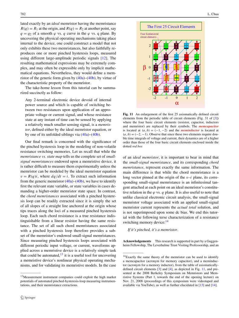
Fig. 11 An enlargement of the first 25 axiomatically defined circuitelements from the periodic table of circuit elements (Fig. 31 of [3])where the four basic circuit elements (resistor, capacitor, inductorsand memristor) are replaced by their symbols. The memcapacitoris located at (a, b) = (−1,−2) and the meminductor is located at(a, b) = (−2,−1). Observe that since these two elements require dou-ble time integrals of voltage and current, their dynamics are of a higherorder than those of the four basic circuit elements enclosed inside thedotted red box
of an ideal memristor, it is important to bear in mind thatthe small-signal memristance, and its corresponding chordmemristance, represent exactly the same information. Themain difference is that while the chord memristance is along vector pinned at the origin of the v–i plane, its corre-sponding small-signal memristance is an infinitesimal tan-gent attached at each point on an ideal memristor’s constitu-tive relation in the ϕ vs. q plane. It is also useful to note thatunlike classical electronic circuit analysis, the small-signalmemristor voltage associated with an applied small-signalmemristor current represents the actual total solution, andis not superimposed upon some dc bias. We end this tutor-ial with the following terse characterization of a resistanceswitching memory device:14
If it’s pinched, it’s a memristor.
Acknowledgements This research is supported in part by a Guggen-heim Fellowship, The Leverhulme Trust Visiting Professorship, and an
14Exactly the same theory of the memristor can be used to identifya memcapacitor (acronym for memory capacitor), and a meminduc-tor (acronym for a memory inductor), from the table of axiomatically-defined circuit elements [3] and [4], as depicted in Fig. 11, and pre-sented at the 2008 Berkeley Symposium on Memristors and Mem-ristive Systems (Part 1, towards the end of the opening lecture) onNov. 21, 2008 (proceedings of this symposium were videotaped andavailable via YouTube), as well as further elucidated in [13] and [14].

Resistance switching memories are memristors 783
AFOSR grant No. FA9550-10-1-0290. The author would like to thankDr. Stan Williams and Dr. Mathew Pickett from hp for stimulating dis-cussions, and to Prof. Hyongsuk Kim and Dr. Valery Sbitnev for theirassistance in the preparation of this paper.
Open Access This article is distributed under the terms of the Cre-ative Commons Attribution Noncommercial License which permitsany noncommercial use, distribution, and reproduction in any medium,provided the original author(s) and source are credited.
References
1. L.O. Chua, IEEE Trans. Circuit Theory CT 18, 507 (1971)2. L.O. Chua, S.M. Kang, Proc. IEEE 64, 209 (1976)3. L. Chua, Nonlinear circuit theory, in Modern Network Theory—
An Introduction: Guest lectures of the 1978 European Conferenceon circuit theory and Design, ed. by G.S. Moschytz, J. Neirynck(Georgi, st-Saphorin, Switzerland, 1978), p. 81
4. L.O. Chua, Proc. IEEE 91, 1830 (2003)5. J.J.B. Jack, D. Noble, R.W. Tsien, Electric Current Flow in Ex-
citable Cells (Oxford University Press, Oxford, 1975)6. M. Itoh, L. Chua, Int. J. Bifur. Chaos 18, 3183 (2008)7. Z. Diao, M. Pakala, A. Panchula, Y. Ding, D. Apalkov, L.-C.
Wang, E. Chen, Y. Huai, J. Appl. Phys. 99, 086510 (2006)8. X. Duan, Y. Huang, C.M. Lieber, Nano Lett. 2, 487 (2002)9. J.W. Bruce, P.J. Giblin, Functions and Singularities (Cambridge
University Press, Cambridge, 1999)10. D.B. Strukov, G.S. Snider, D.R. Stewart, R.S. Williams, Nature
453, 80–83 (2008)11. R. Waser, M. Aono, Nat. Mater. 6, 833 (2007)12. L. Chua, IEEE Trans. Circuits Syst. CAS-27, 1014 (1980)13. L.O. Chua, Introduction to Memristors, IEEE Expert Now Educa-
tion Course, IEEE (2010)14. M. Di Ventra, Y.V. Pershin, L.O. Chua, Proc. IEEE 97, 1717
(2009)