rev 0.2 technical description - farnell element14 · serial port configuration (default) port 0:...
TRANSCRIPT

REV 0.2
TECHNICAL DESCRIPTION
Fastrax Mini Evaluation kit This document describes the electrical connectivity and main functionality of the Mini Evaluation kit hardware.
September 10th , 2007
Fastrax Ltd.

2008-03-11 Page 2 of 15
MEVKTB_Tech_doc_rev_0 2.doc
TRADEMARKS iTraxTM, iSuiteTM, iSysTM and iTalkTM are trademarks of Fastrax Ltd. Microsoft Windows NT®, Microsoft Windows 2000®, Microsoft Windows XP®, and Microsoft Visual C++® are registered trademarks of Microsoft® Corporation. MATLAB® is a registered trademark of MathWorks, Inc. All other trademarks are trademarks or registered trademarks of their respective holders.
2008-03-11 Page 3 of 15
MEVKTB_Tech_doc_rev_0 2.doc
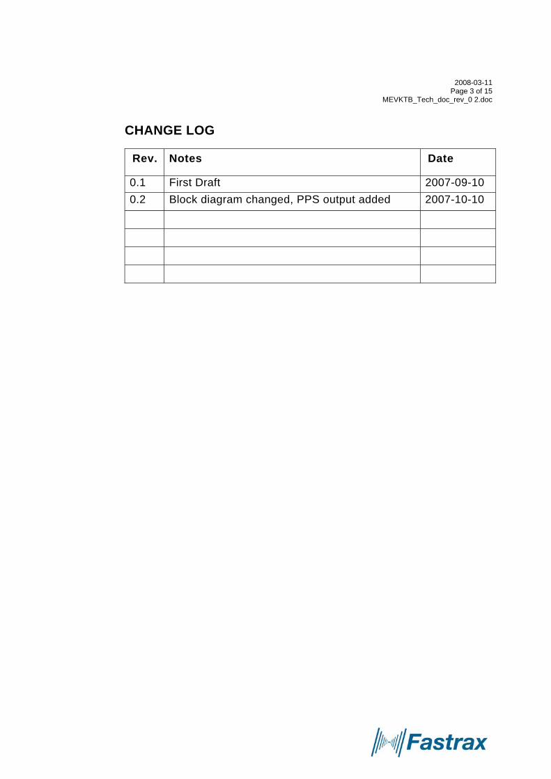
CHANGE LOG
Rev. Notes Date
0.1 First Draft 2007-09-10 0.2 Block diagram changed, PPS output added 2007-10-10

2008-03-11 Page 4 of 15
MEVKTB_Tech_doc_rev_0 2.doc
CONTENTS
REV 0.1 .................................................................................................................... 1
FASTRAX MINI EVALUATION KIT .......................................................................... 1
1.
GENERAL DESCRIPTION .............................................................................. 6
1.1
Block diagram ...................................................................................... 7
2.
SPECIFICATIONS........................................................................................... 8
2.1
General ................................................................................................. 8
2.2
Absolute maximum ratings.................................................................. 8
3.
CONNECTIVITY .............................................................................................. 9
3.1
Connection assignments ..................................................................... 9
2008-03-11 Page 5 of 15
MEVKTB_Tech_doc_rev_0 2.doc
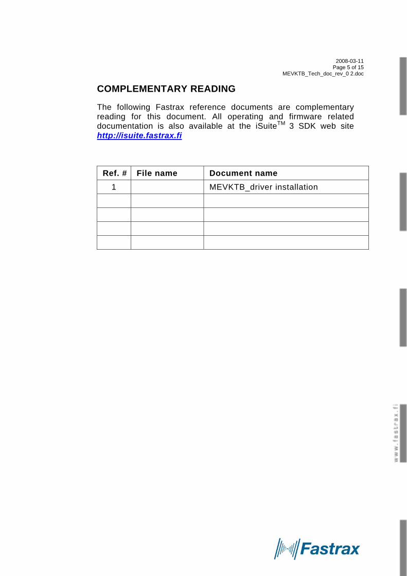
COMPLEMENTARY READING
The following Fastrax reference documents are complementary reading for this document. All operating and firmware related documentation is also available at the iSuiteTM 3 SDK web site http://isuite.fastrax.fi
Ref. # File name Document name 1 MEVKTB_driver installation

2008-03-11 Page 6 of 15
MEVKTB_Tech_doc_rev_0 2.doc
1. GENERAL DESCRIPTION
The Mini Evaluation kit is a small, compact, PCB meant for evaluating and testing of iTrax03, iTrax100, iTrax300 and uPatch Families. The basic idea of Mini Evaluation kit is the same as iTrax03 Evaluation Kit’s, to provide a pc-interface for GPS-modules.
The Mini Evaluation kit is interfaced via USB cable and it’s also pow-ered from the USB so no external power is needed. The Evaluation Kit has the following connectivity:
• 40-pin socket for iTrax Application Boards
• uPatch130/uPatch300 connector
• Two USB connectors (Mini-B)
• Reset switch
• Programming switch for firmware upgrade
• PPS signal in pinheader
• General I/O lines can be probed from 40-pin socket- connector if needed
Figure 1 Mini Evaluation Kit with iTrax03s application board.
2008-03-11 Page 7 of 15
MEVKTB_Tech_doc_rev_0 2.doc
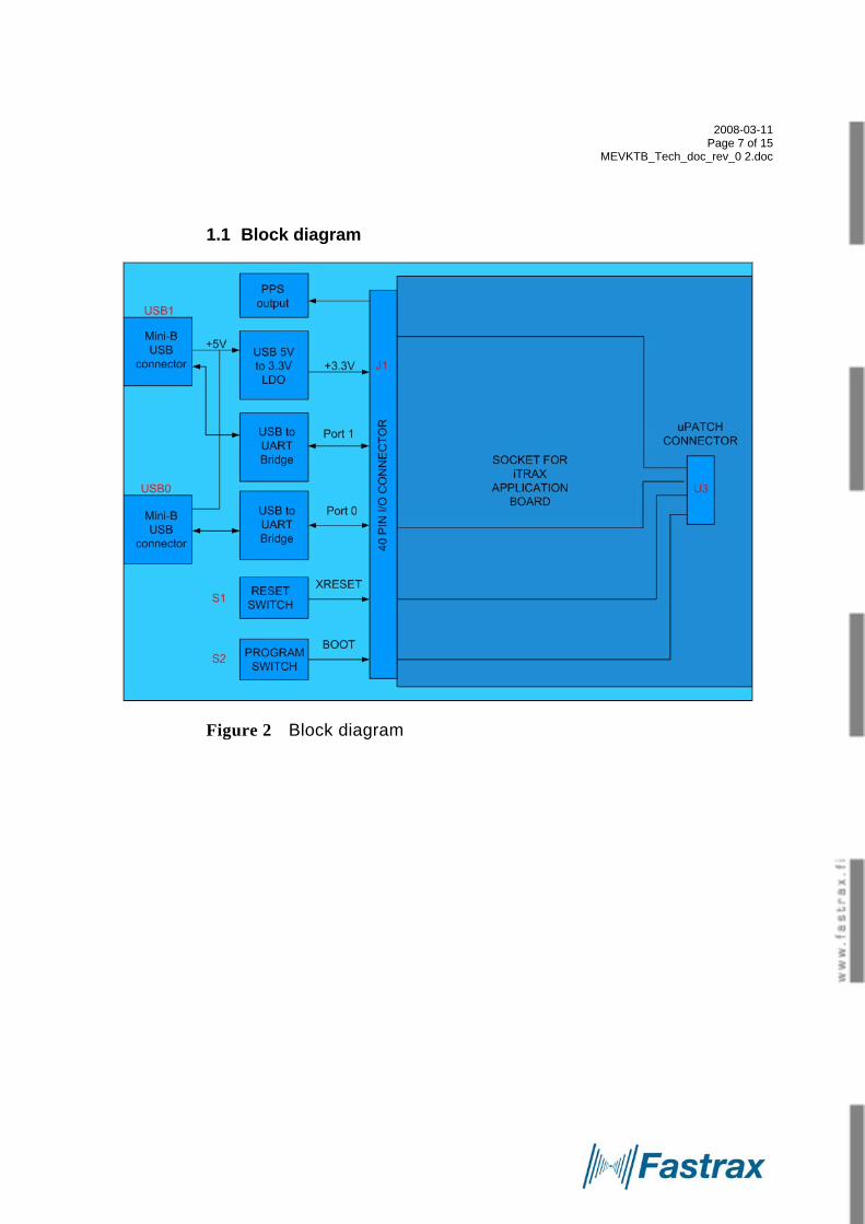
1.1 Block diagram
Figure 2 Block diagram
2008-03-11 Page 8 of 15
MEVKTB_Tech_doc_rev_0 2.doc
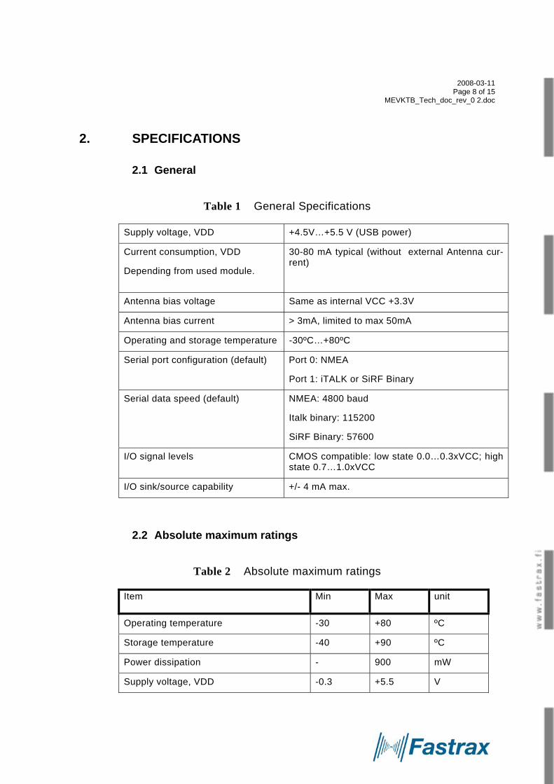
2. SPECIFICATIONS
2.1 General
Table 1 General Specifications
Supply voltage, VDD +4.5V…+5.5 V (USB power)
Current consumption, VDD
Depending from used module.
30-80 mA typical (without external Antenna cur-rent)
Antenna bias voltage Same as internal VCC +3.3V
Antenna bias current > 3mA, limited to max 50mA
Operating and storage temperature -30ºC…+80ºC
Serial port configuration (default) Port 0: NMEA
Port 1: iTALK or SiRF Binary
Serial data speed (default) NMEA: 4800 baud
Italk binary: 115200
SiRF Binary: 57600
I/O signal levels CMOS compatible: low state 0.0…0.3xVCC; high state 0.7…1.0xVCC
I/O sink/source capability +/- 4 mA max.
2.2 Absolute maximum ratings
Table 2 Absolute maximum ratings
Item Min Max unit
Operating temperature -30 +80 ºC
Storage temperature -40 +90 ºC
Power dissipation - 900 mW
Supply voltage, VDD -0.3 +5.5 V

2008-03-11 Page 9 of 15
MEVKTB_Tech_doc_rev_0 2.doc
3. CONNECTIVITY
3.1 Connection assignments
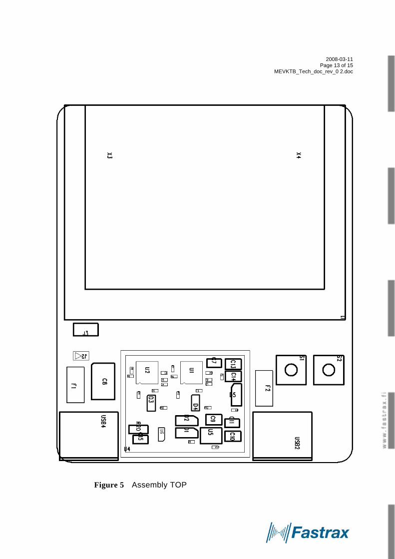
Figure 3 Overview of the Mini Evaluation Kit’s card holder
The circuit board size is 72.0mm (width) x 61.2mm (length). General tolerance is ±0.3mm.
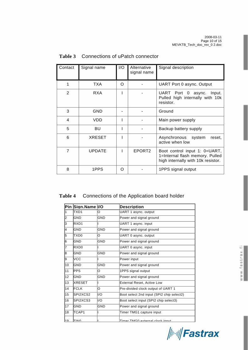
The uPatch connector is an 8-pin interface connector. The connector is from JST, type SM08B-SURS-TF. Mating connector is e.g. JST 08SUR-32S.
Table 3 describes the connectivity and signals of this connector. Table 4 describes the connectivity and signals of the Application board holder
2008-03-11 Page 10 of 15
MEVKTB_Tech_doc_rev_0 2.doc
Table 3 Connections of uPatch connector
Contact Signal name I/O Alternative signal name
Signal description
1 TXA O - UART Port 0 async. Output
2 RXA I - UART Port 0 async. Input. Pulled high internally with 10k resistor.
3 GND - - Ground
4 VDD I - Main power supply
5 BU I - Backup battery supply
6 XRESET I - Asynchronous system reset, active when low
7 UPDATE I EPORT2 Boot control input 1: 0=UART, 1=Internal flash memory. Pulled high internally with 10k resistor.
8 1PPS O - 1PPS signal output
Table 4 Connections of the Application board holder
Pin Sign.Name I/O Description1 TXD1 O UART 1 async. output
2 GND GND Power and signal ground
3 RXD1 I UART 1 async. input
4 GND GND Power and signal ground
5 TXD0 O UART 0 async. output
6 GND GND Power and signal ground
7 RXD0 I UART 0 async. input
8 GND GND Power and signal ground
9 VCC I Power input
10 GND GND Power and signal ground
11 PPS O 1PPS signal output
12 GND GND Power and signal ground
13 XRESET I External Reset, Active Low
14 FCLK O Pre-divided clock output of UART 1
15 SPI2XCS2 I/O Boot select 2nd input (SPI2 chip select2)
16 SPI2XCS3 I/O Boot select input (SPI2 chip select3)
17 GND GND Power and signal ground
18 TCAP1 I Timer TMG1 capture input
19 TIN0 I Timer TMG0 external clock input

2008-03-11 Page 11 of 15
MEVKTB_Tech_doc_rev_0 2.doc
20 TIN1 I Timer TMG1 external clock input
21 GND GND Power and signal ground
22 TCAP0 I Timer TMG0 capture input
23 PM1 I Pulse measurement input 1
24 PM0 I Pulse measurement input 0
25 GND GND Power and signal ground
26 MMCCMD I/O UI indicator B output (MMC command bus)
27 SPI1XCS0 I/O Power Good control input (SPI1 cs 0)
28 MMCCLK O MMC clock output
29 SPI1CLK O SPI1 clock
30 MMCDAT I/O UI indicator A output (MMC data bus)
31 GND GND Power and signal ground
32 SPI1SDO O SPI1 data output
33 GND GND Power and signal ground
34 SPI1SDI I SPI1 data input
35 GND GND Power and signal ground
36 SPI2CLK I/O SPI2 clock, output in master mode
37 GND GND Power and signal ground
38 SPI2SDI I ON/OFF control input (SPI2 data input)
39 GND GND Power and signal ground
40 SPI2SDO O UI indicator C output (SPI2 data output)
Table 5 Signals of the USB Mini-B connector
Contact Number Signal Name Typ. wiring assignment 1 VBUS Red
2 D- White
3 D+ Green
4 ID Not connected
5 GND Black
Shell Shield Drain Wire

2008-03-11 Page 12 of 15
MEVKTB_Tech_doc_rev_0 2.doc
Figure 4 USB Mini-B type connector and pin assignments.
2008-03-11 Page 13 of 15
MEVKTB_Tech_doc_rev_0 2.doc
Figure 5 Assembly TOP

2008-03-11 Page 14 of 15
MEVKTB_Tech_doc_rev_0 2.doc
REF. QTY TECHNICALDESCRIPTION VALUE PCB Part TypeC1 1 Capacitor chip 1uF 6 3V +-20% X5R 0402 1uF C0402 C/0402/X5R/1U/6V3/T20C2 1 Capacitor chip, 100nF 6.3V +-20% X5R 0402 100nF C0402 C/0402/X5R/100N/6V3/T20 C3 1 Capacitor chip, 1uF 6.3V +-20% X5R 0402 1uF C0402 C/0402/X5R/1U/6V3/T20 C4 1 Capacitor chip, 1uF 6.3V +-20% X5R 0402 1uF C0402 C/0402/X5R/1U/6V3/T20 C5 1 Capacitor chip, 100nF 6.3V +-20% X5R 0402 100nF C0402 C/0402/X5R/100N/6V3/T20 C6 1 Capacitor chip, 1uF 6.3V +-20% X5R 0402 1uF C0402 C/0402/X5R/1U/6V3/T20 C7 1 Capacitor chip, 220nF 16V 10% X7R 0603 220nF 16V C0603 C/0603/X7R/220N/16V C8 1 Capacitor tantal, 100uF 10V 10% D 100uF 10V TAJ_D C/D/TANT/100U/10V C9 1 Capacitor chip, 4,7uF 6,3V X5R 0805 +-20% 4u7F C0805 C/0805/X5R/4U7/6V3/T5P C10 1 Capacitor chip, 4,7uF 6,3V X5R 0805 +-20% 4u7F C0805 C/0805/X5R/4U7/6V3/T5P C11 1 Capacitor chip, 100nF 16V 10% X7R 0603 100nF/16V C0603 C/0603/X7R/100N/16V/T20P C12 1 Capacitor chip, 10nF 16V 10% X7R 0402 10nF C0402 C/0402/X7R/10N/16V/T10P C13 1 Capacitor chip, 4,7uF 6,3V X5R 0805 +-20% 4u7F C0805 C/0805/X5R/4U7/6V3/T5P C14 1 Capacitor chip, 4,7uF 6,3V X5R 0805 +-20% 4u7F C0805 C/0805/X5R/4U7/6V3/T5P C15 1 Capacitor chip, 220nF 16V 10% X7R 0603 220nF 16V C0603 C/0603/X7R/220N/16V D1 1 Diode 75V 225mA, BAT54J 75V 225mA SOD323 D/75V/225MA/BAT54J D2 1 Diode 75V 225mA, BAT54J 75V 225mA SOD323 D/75V/225MA/BAT54J D3 1 TVS Diode SOT23-6 Bidirectional, ESDA6V1BC6 SUPERSOT6 D/ESDA6V1BC6 D4 1 TVS Diode SOT23-6 Bidirectional ESDA6V1BC6 SUPERSOT6 D/ESDA6V1BC6 D5 1 Diode 75V 225mA, BAT54J 75V 225mA SOD323 D/75V/225MA/BAT54J F1 1 Fuse 1A R452001.MRL SMDLITTELFUSE F/LITTELFUSE1A F2 1 Fuse 1A R452001.MRL SMDLITTELFUSE F/LITTELFUSE1A J1 1 2x20 pin Flex Card Terminal 2x20 J/2x20/2P0_FLEX FLEX_CARD_T J2 1 LED BLUE AP1608MBC 0603_KINGBRIGHT D/LED/BLUE/AP1608MBC J3 1 1x2 pin-header, straight, pitch 2.54mm 1x2P2.54 CON/2X1/2P54 J/1X2/0/2P54 L3 1 75R,+-25%@100MHz, 0R4@DC, 300mA BLM15BB750 L0402 L/0402/BLM15BB750PN1D L4 1 75R,+-25%@100MHz, 0R4@DC, 300mA BLM15BB750 L0402 L/0402/BLM15BB750PN1D L5 1 75R,+-25%@100MHz, 0R4@DC, 300mA BLM15BB750 L0402 L/0402/BLM15BB750PN1D L6 1 75R,+-25%@100MHz, 0R4@DC, 300mA BLM15BB750 L0402 L/0402/BLM15BB750PN1D L7 1 75R,+-25%@100MHz, 0R4@DC, 300mA BLM15BB750 L0402 L/0402/BLM15BB750PN1D L8 1 75R,+-25%@100MHz, 0R4@DC, 300mA BLM15BB750 L0402 L/0402/BLM15BB750PN1D L9 1 75R,+-25%@100MHz, 0R4@DC, 300mA BLM15BB750 L0402 L/0402/BLM15BB750PN1D L10 1 75R,+-25%@100MHz, 0R4@DC, 300mA BLM15BB750 L0402 L/0402/BLM15BB750PN1D R1 1 Resistor chip, 470R 5% 0402 63mW 470R R0402 R/0402/470R/5P/G R2 1 Resistor chip, 10k 5% 0402 63mW 10k R0402 R/0402/10K/T5P/G R3 1 Resistor chip, 10k 5% 0402 63mW 10k R0402 R/0402/10K/T5P R4 1 Resistor chip, 10k 5% 0402 63mW 10k R0402 R/0402/10K/T5P R5 1 Resistor chip, 2k2 5% 0402 63mW 2.2k, 5% R0402 R/0402/2K2/T5P R6 1 Resistor chip, 330R 5% 0402 63mW 330R R0402 R/0402/330R/5P/G R7 1 Resistor chip, 330R 5% 0402 63mW 330R R0402 R/0402/330R/5P/G R8 1 Resistor chip, 330R 5% 0402 63mW 330R R0402 R/0402/330R/5P/G R9 1 Resistor chip, 330R 5% 0402 63mW 330R R0402 R/0402/330R/5P/G R10 1 Resistor chip, 100R 5% 0402 63mW 100R R0402 R/0402/100R/T5P/G R11 1 Resistor chip, 100R 5% 0402 63mW 100R R0402 R/0402/100R/T5P/G R12 1 Resistor chip, 100R 5%0402 63mW 100R R0402 R/0402/100R/T5P/G R13 1 Resistor chip, 100R 5% 0402 63mW 100R R0402 R/0402/100R/T5P/G R20 1 47R 5% 0603 100mW 50V 47R R0603 R/0603/47R/T5P/G S1 1 Switch, SMD PUSH BUTTON SW SW/B3S-1000 SW/PUSHBUTTON S2 1 Switch, SMD PUSH BUTTON SW SW/B3S-1000 SW/PUSHBUTTON SC1 1 Rubber feet, RBS-27 BL RBS-27 BL RUBBER_FEET SC/RBS-27BL SC2 1 Rubber feet, RBS-27 BL RBS-27 BL RUBBER_FEET SC/RBS-27BL SC3 1 Rubber feet, RBS-27 BL RBS-27 BL RUBBER_FEET SC/RBS-27BL SC4 1 Rubber feet, RBS-27 BL RBS-27 BL RUBBER_FEET SC/RBS-27BL U1 1 USB /RS232 driver, CP2102 CP2102 QFN28_CP2101 U/USB/CP2102 U2 1 USB /RS232 driver, CP2102 CP2102 QFN28_CP2101 U/USB/CP2102 U3 1 Connector, SUR 0.8 pitch 8 pin nichiatsu P1276 P1276_PCB_DECAL J/P1276 U4 1 Shield, SHIELD SHIELD SHIELD U5 1 Reg. 3V3, 150mA 3V3, 150mA SOT23-5 U/LP2985/3V3 U6 1 1.5A LDO Positive Regulator NC7SZ125M5 SOT23-5 U/NC7SZ125 USB2 1 USB connector, SMD with plastic pegs Molex J/USB/67503_1020 J/USB/MOLEX_67503_1020 USB4 1 USB connector, SMD with plastic pegs Molex J/USB/67503_1020 J/USB/MOLEX_67503_1020
Figure 6 Bill of materials
2008-03-11 Page 15 of 15
MEVKTB_Tech_doc_rev_0 2.doc
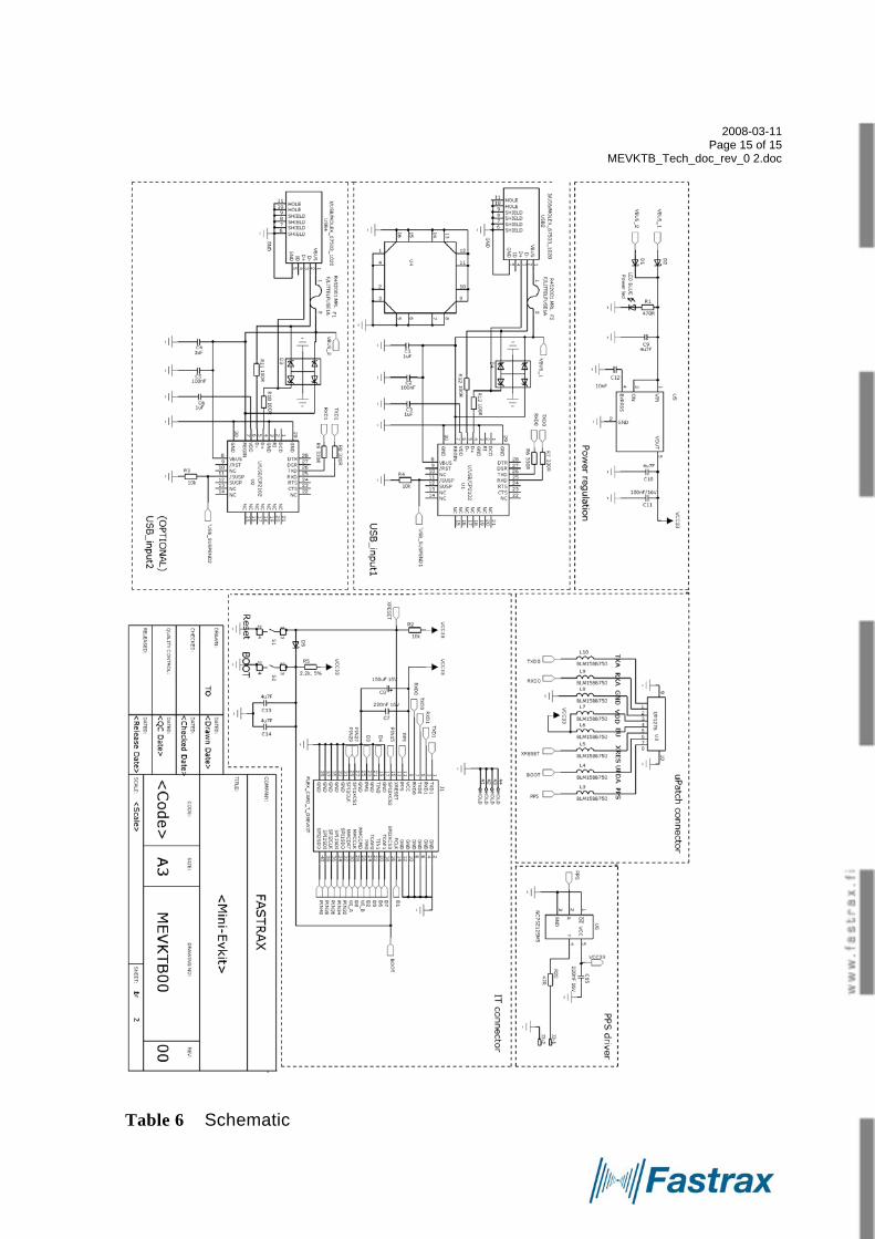
Table 6 Schematic