revision exercise 1 soln - webs microcontroller applications exercise 3 -1- revision exercise 1 q1...
TRANSCRIPT

EEE3410 MICROCONTROLLER APPLICATIONS EXERCISE 3
-1-
REVISION EXERCISE 1 Q1
Q1 Soln Ch 1
Ch 1 Slide 25 Q2 Ch 5
Q2 Soln
Ch 5 Slide 5 Q3
Q3 Soln
# - immediate, Hex No.-Direct, Register Label – Register, @ - Indirect, Short Jump - Relative @ + - Indexed ACALL, AJUMP – Absolute LCALL, LJUMP - Long
Q4
Q4 Soln
Without the Label “H” at the end of the number #30, #30 is considered as decimal no. A: 30(10)=1EH = 0001 1110 ⇒ RL A ⇒ 0011 1100 = 3CH (RL Rotate Left by 1 bit) ← 0
← 0
← 0
← 0
← 1
← 1
← 1
← 1
←0
←
0 0 1 1 1 1 0 0 0011 1100 ANL (AND Logic) 1111 0000 (#F0H) = 0011 0000 (30H) 0 0 1 1 1 1 0 0 A
AND 1 1 1 1 0 0 0 0 #0F0H = 0 0 1 1 0 0 0 0 #30H

EEE3410 MICROCONTROLLER APPLICATIONS EXERCISE 3
-2-
Line 1-Content of A: 1EH Line 2–Content of A : 3CH Line 3 – Content of A:30H Q5
Q5 Soln
← MOV DESTINATION, SOURCE
Q6
Q6 Soln
Starting Address of Program Starting Address R0 = R0 + 1 CJNE – COMPARE R0 = 80H ? JUMP to AGAIN IF NOT EQUAL else STOP
Q7
Q7 Soln
Lecture 8, Slide 19 (3 INTERNAL , 2 EXTERNAL)
Q8
Q8 Soln
Ch5 Slide 13,14 , Directives – how to compile the program? Q9
Q9 Soln Ch 4
1. RAM 2. ROM 3. I/O ports 4. Serial COM Port 5. Timer
Q10

EEE3410 MICROCONTROLLER APPLICATIONS EXERCISE 3
-3-
Q10 Soln Ch 4
00 Bank 0, 01 Bank 1, 10 Bank 2, 11 Bank 3 (b) Set the register select bits (RS0 and RS1) of the Program Status Word (PSW) to 1.
Q11
(a) a hexadecimal number (b) a binary number (c) a BCD number Q11 Soln
Q12
Q12 Soln
1011 0101 =(-1)x[1+4+16+32]=-53 1111 0101=(-1)x[1+4+16+32+64]=-117
Q13 Q13 Soln
2’ complement = 1’s complement + 1 = 1101 1010 + 1 = 11011011
Result = 1001 0110 ⇒⇒⇒⇒1001 0110-1 = 1001 0101⇒⇒⇒⇒Magnitude=0110 1010=106
Q15
Q15 Soln
# - Immediate, Hex Code – Direct, Register Label – Register @ - Indirect, @ + - Indexed

EEE3410 MICROCONTROLLER APPLICATIONS EXERCISE 3
-4-
Line 2 – Immediate addressing Line 3 – Register addressing Line 4 – Register Indirect addressing A=10H
Q16
Q16 Question
Solution
2. A=30H=0011 0000 ⇒⇒⇒⇒ RL (Rotate Left) ⇒⇒⇒⇒ 0110 0000 = 60H 3. CPL A (Complement all the bits in A, 0→→→→1, 1→→→→0) 0110 0000 ⇒⇒⇒⇒ 1001 1111 = 9FH
4. MUL AB (Multiply AB), High Byte in B, Low Byte in A 9FH = 159 (dec) , 9FH x 03H = 159 x 3 = 477 (dec) = 01DD H, B = 01H, A = 0DDH
Q17
Q17 Soln
*Refer to Q6 COMPARE R0=70H? Jump to AGAIN IF NOT EQUAL Else END
Q18
Q18 Soln
Vref = 2 x 2, 28 = 256, 255 intervals, 1 bit increment = 2 x 2 / 255 0V →→→→ 0 dec, 4V→→→→255 dec
Q19

EEE3410 MICROCONTROLLER APPLICATIONS EXERCISE 3
-5-
Q19 Soln (a)
8-bit unsigned : 0 … 28 – 1, 8-bit signed number -(27-1) … (27-1), -127….-1, 0 …. 127 8-bit 2’s complement -28 …. (27-1)
(b) +59 = 0011 1011, 1’s complement = 1100 0100 2’s complement = 1100 0101
(c )
Q20
Clear Carry 1111 1111→→→→ P1 All LED ON 8 Counts for 1 cycle Rotate Left with Carry 1111 1110 bit0 OFF 1111 1101 1111 1011 : 1 1+ 1 [1+ 2 (2x248)+ 2 2]x200+ 2 2
Q20

EEE3410 MICROCONTROLLER APPLICATIONS EXERCISE 3
-6-
Q20 Soln (a)
Lecture 6 Slide 60-63 SJMP : offset 1 byte (2’s complement) (-128 →→→→127) AJMP : 11 bit address, 211=2048 LJMP : 16 bit address, 216=64K
(b)
*ENDING CONDITIONS Q21
Lecture 8 Slide 17 (i), (iv), (iii), (v), (vi), (ii)
EEE3410 MICROCONTROLLER APPLICATIONS EXERCISE 3
-7-
Q21 Soln (a)

EEE3410 MICROCONTROLLER APPLICATIONS EXERCISE 3
-8-
Q21 Soln(b)
SUBB Subtract with borrow, if P0 < 10 then Carry will be set (borrow) ⇒⇒⇒⇒ Goto display else Set display character R0 = “E” = the 10th entry
Q22

EEE3410 MICROCONTROLLER APPLICATIONS EXERCISE 3
-9-
Starting Location of Square Table Set P0 as Input Port Read P0 Loop Up “Square Table” (the “DPTR + P0” entry) Move result to P1 Delay Go BACK Square Table Delay Routine 1 1+ 1 [1+ 2 (2x255)+ 2 2]x200+ 2 2
Q22 Soln (a)
Q22 Soln (b)
Q22 Soln (c)

EEE3410 MICROCONTROLLER APPLICATIONS EXERCISE 3
-10-
Q25 Ch 4
Q25 Soln
Using EA (External Access) pin to control External RAM
Q26
Q26 Soln
Q27
Q27 Soln
Q28
Q28 Soln
Refer to Q3

EEE3410 MICROCONTROLLER APPLICATIONS EXERCISE 3
-11-
Q29
S29 Soln
Lecture 8, Slide 19
Q30
Q30 Soln
Q31
Q31 Soln
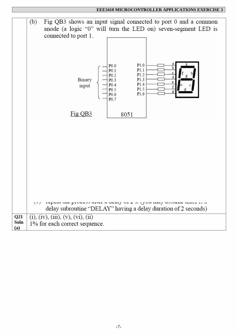
COMMON ANODE Q32

EEE3410 MICROCONTROLLER APPLICATIONS EXERCISE 3
-12-
Q32 Soln
SP = 07H, R3 = A4, R1 = 55 PUSH 3; SP=SP+1=08H, Data at 3 (R3)→→→→08H PUSH 1;SP=SP+1=09H, Data at 1 (R1) →→→→09H After ACALL, Return address = 0A push into stack at 0AH
Q33

EEE3410 MICROCONTROLLER APPLICATIONS EXERCISE 3
-13-
Q33 Soln
Compare Jump Not Equal to L1 If EQUAL Jump to L2 Jump Carry to L2, If A > #0B0H ⇒⇒⇒⇒ INC R2 If A ≤ #0B0H ⇒⇒⇒⇒ DEC R1
Q34
Q34 Soln
X at 30H →→→→ A Y at 31H →→→→ B DIV AB A ÷ B = Quotient in A & Remainder in B Quotient in A →→→→ 10H, Remainder in B→→→→11H
Q35
Q35 Soln (a)
1’s complement = 10010101 – 1 = 1001 0100 ⇒⇒⇒⇒Invert all bit ⇒⇒⇒⇒ 01101011=1+2+8+32+64=107, Magnitude = 0110 1011 = 107 ⇒⇒⇒⇒ number = -10710
(b)
(i) Result after addition is 1010 1011 2’s complement = 1010 1011 1’s complement = 1010 1010 Magnitude = 0101 0101 =1+4+16+64=85 No. = -85
(ii) )*Neglect bit 8 at the LEFT after addition

EEE3410 MICROCONTROLLER APPLICATIONS EXERCISE 3
-14-
Q36

EEE3410 MICROCONTROLLER APPLICATIONS EXERCISE 3
-15-
Q36 (a) (b) (c) Soln (d)
1 1+ 1 [1+ 1 (1+ 1 1+ 2 2)x250+ 2 2]x200+ 2 2
(e)
(f)
1 1+ 1 1+ 1 [1+ 1 (1+ 1 1+ 2 2)x250+ 2 2]x200+ 2 2x10+ 2 2
Q37

EEE3410 MICROCONTROLLER APPLICATIONS EXERCISE 3
-16-
Q37 Soln (a)
Step Size = Vref / [2n-1] n : No. of bits of ADC
(b)
-55 oC ⇒⇒⇒⇒ 0V⇒⇒⇒⇒ 0H (120 – (-55)) x 10mV/ oC = ∆∆∆∆V V = V ( -55oC) + ∆∆∆∆V = 0+(120+55)x10 = 1750mV 1750 / Step size = 175 decimal
(c)

EEE3410 MICROCONTROLLER APPLICATIONS EXERCISE 3
-17-
Since 1 D-type flip-flop ⇒⇒⇒⇒frequency divide by 2 (d)

EEE3410 MICROCONTROLLER APPLICATIONS EXERCISE 3
-18-
REVISION EXERCISE 2 Q1 State five 8051 microcontroller on-chip components that could not be found on a
general purpose microprocessor. Q1 Soln
1. RAM 2. ROM 3. I/O ports 4. Serial COM port 5. Timer
Q2 Fig A2 shows the memory map of 8051 on-chip memory. Give the address range of memory segments A – G as indicated in the Figure.
Fig. A2 Q2 Soln
A : 00H – 07H B : 08H – 0FH C : 10H – 17H D : 18H – 1FH E : 20H – 2FH (16 bytes) F : 30H – 7FH G : 0000H – 0FFFH, 00H - 7FH= 0 - 0111 1111 =0.. 27=0..128 = 128 byte RAM 0000H … 0FFFH = 0 … 212=4096=4K ROM
Q3 The following 8051 program evaluates the sum of integers from 1 to 10. Add Machine Code
0000 E4 0001 78 0002 0A 0003 28 0004 D8 0005 FD (-3 dec) 0006
(a) State the function of register R0 in the program. (b) Give the values stored in the registers A and R0 at the end of program execution. (c) Explain how the machine code “FD” in address 0005H is obtained.
Q3 Soln
(a) The function of R0 is (counter) to use to produce the integers from 1 to 10. (b) A = 1+2+3+4+5+6+7+8+9+10=55 decimal (or 37H) and R0 = 0 (or 00H) (c) Code in 0005H = 0003H – 0006H = FDH, Without Jump action, next address is 0006 If program jump occurs, jump to “AGAIN at 0003” 0006 + offset, offset = FD DJNZ uses relative address, 0003-0006 = -3 decimal, 3=0000 0011b, 1’s complement = 1111 1100 ⇒ 2’s complement=1111 1100 + 1 = 1111 1101 = FDH
Q4 (a) Give any 4 differences between microprocessor and microcontroller. (b) What is the power-up reset value for the stack point (SP) of the 8051.

EEE3410 MICROCONTROLLER APPLICATIONS EXERCISE 3
-19-
Q4 Soln
(b) 07H Q5 Show all the steps clearly to convert the number 97610 to
(a) a hexadecimal number; (b) a binary number. Q5 Soln
Q6 What are the decimal values of the 8-bit binary number 1000 0101, if it is read as:
(a) a 8-bit unsigned number; (b) a 8-bit signed number; (c) a 8-bit BCD number.
Q6 Soln
The decimal equivalent of 1000 0101 (a) 8-bit unsigned number: 1000 0101=128 + 4 + 1 = 133 (b) 8-bit signed number: 1000 0101= -(4 + 1 ) = - 5 (c) 8-bit BCD number = 85 [ 8 → 1000, 5 → 0101 ]
Q7 Using 8-bit 2’s complement arithmetic to calculate (-27)10 – (89)10. Q7 Soln
1’s complement = 1000 1100 – 1 = 1000 1011→0111 0100 →No. = -(4+16+32+64)
Q8 Refer to the instructions in Table A8.
(a) State the addressing mode for Line 1. (b) State the addressing mode for Line 2. (c) State the addressing mode for Line 3. (d) State the addressing mode for Line 4. (e) Briefly explain why the instruction in
Line 5 is illegal?
Q8 Soln
(a) Register Addressing Mode (b) Immediate Addressing Mode (c) Direct Addressing Mode (d) Indirect Addressing Mode (e) Only direct addressing mode is allowed for pushing onto the stack
EEE3410 MICROCONTROLLER APPLICATIONS EXERCISE 3
-20-
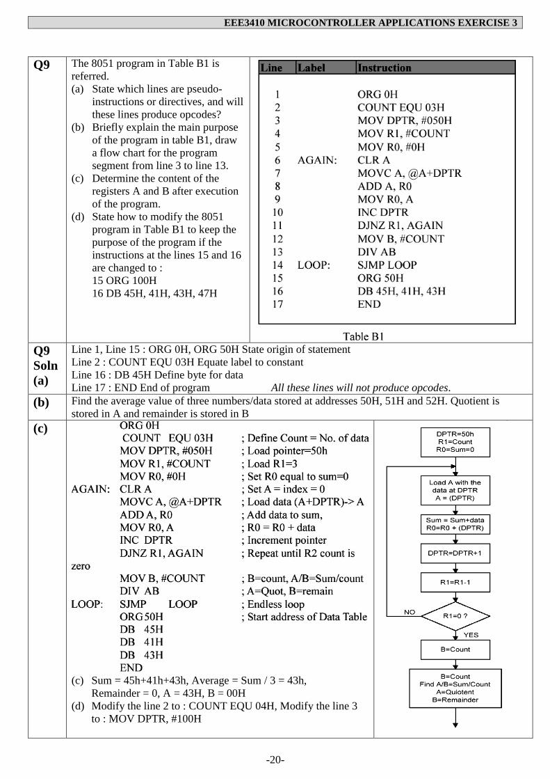
Q9 The 8051 program in Table B1 is
referred. (a) State which lines are pseudo-
instructions or directives, and will these lines produce opcodes?
(b) Briefly explain the main purpose of the program in table B1, draw a flow chart for the program segment from line 3 to line 13.
(c) Determine the content of the registers A and B after execution of the program.
(d) State how to modify the 8051 program in Table B1 to keep the purpose of the program if the instructions at the lines 15 and 16 are changed to : 15 ORG 100H 16 DB 45H, 41H, 43H, 47H
Q9 Soln (a)
Line 1, Line 15 : ORG 0H, ORG 50H State origin of statement Line 2 : COUNT EQU 03H Equate label to constant Line 16 : DB 45H Define byte for data Line 17 : END End of program All these lines will not produce opcodes.
(b) Find the average value of three numbers/data stored at addresses 50H, 51H and 52H. Quotient is stored in A and remainder is stored in B
(c)
(c) Sum = 45h+41h+43h, Average = Sum / 3 = 43h, Remainder = 0, A = 43H, B = 00H (d) Modify the line 2 to : COUNT EQU 04H, Modify the line 3
to : MOV DPTR, #100H

EEE3410 MICROCONTROLLER APPLICATIONS EXERCISE 3
-21-
Q10 Fig. B2a shows a circuit diagram of connecting 8 LEDs to the Port 0 of an 8051 microcontroller. Table B2 gives an incomplete program which controls the 8 LEDs to light up continuously as the sequence shown in Fig. B2b. The on/off pattern of the LEDs are encoded and stored in a data table (label as DTBS) inside the program. The following gives the flow of the program. (1) Look up an on/off pattern of LEDs from the data table DTBS. (2) Send the code to Port 0. (3) Perform time delay (4) Go back to step 1 after time delay. A subroutine called DELAY is also given in program to perform time delay.
0111 1110b=7EH 0011 1100b=3CH 0001 1000b=18H 1110 0111b=E7H 1010 0101b=A5H 0101 1010b=5AH
(a) What are the logic levels to turn the LEDs on/off at Port 0?
(b) Complete the program in Table B2.
(c) Find the time delay for the DELAY subroutine. (Assume a 12 MHz clock is used).
Q10 Soln
(a) Logic 0 – LED is ON Logic 1 – LED is OFF
(b)
Q10 (b) Soln

EEE3410 MICROCONTROLLER APPLICATIONS EXERCISE 3
-22-
Q10 (c) Soln
1 Machine Cycle=12/(12x106) =1µµµµs =1+ [1+ (1 + 2)x200+ 2]x250+ 2
Time Delay =1+[1+(1+2)x200+2]x250+2x1µs = 150753 µs or 0.15s
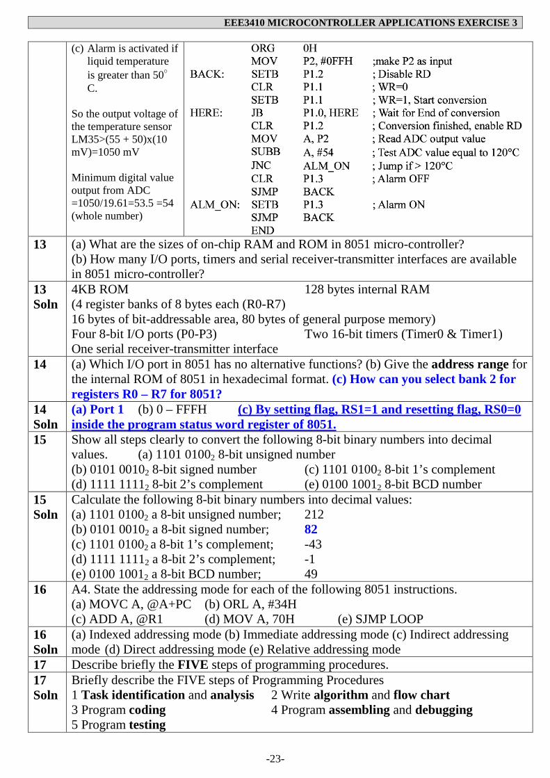
Q11 The temperature of a liquid is monitored by a microcontroller system. The system consists of an 8051 microcontroller, an analogue-to-digital converter ADC0804, a temperature sensor (LM35) and an alarm. If the liquid temperature exceeds 50oC, the 8051 will send a signal to activate the alarm by sending a ‘1’ to the alarm device which is connected to its port pin P1.3. The specifications of the system are given below. (1) Temperature sensor (LM35): (i) the temperature range of the temperature sensor LM35 is -55°C to 150°C and its output scale is 10mV/°C, and (ii) the output value of the ADC0804 is 00H when the LM35 senses -55°C. (2) Analogue-to-digital converter (ADC0804) Voltage of pin Vref/2 = 2.5V (3) Port pin connection of 8051
(a) Draw the circuit diagram of the 8051 microcontroller system according to the given specifications.
(b) Find the step size of the ADC0804.
(c) Determine the minimum output value of the ADC0804 that will activate the alarm.
(d) Write an assembly language program for the 8051 microcontroller system to monitor the liquid temperature.
Q11 Soln
(a) Voltage fed to pin Vref/2 = 2.5V, Conversion range of
the ADC = 2x2.5 = 5V (b) Step size = (2x2.5)/255 =
19.61mV
EEE3410 MICROCONTROLLER APPLICATIONS EXERCISE 3
-23-
(c) Alarm is activated if liquid temperature is greater than 50°C.
So the output voltage of the temperature sensor LM35>(55 + 50)x(10 mV)=1050 mV Minimum digital value output from ADC =1050/19.61=53.5 =54 (whole number)
13 (a) What are the sizes of on-chip RAM and ROM in 8051 micro-controller? (b) How many I/O ports, timers and serial receiver-transmitter interfaces are available in 8051 micro-controller?
13 Soln
4KB ROM 128 bytes internal RAM (4 register banks of 8 bytes each (R0-R7) 16 bytes of bit-addressable area, 80 bytes of general purpose memory) Four 8-bit I/O ports (P0-P3) Two 16-bit timers (Timer0 & Timer1) One serial receiver-transmitter interface
14 (a) Which I/O port in 8051 has no alternative functions? (b) Give the address range for the internal ROM of 8051 in hexadecimal format. (c) How can you select bank 2 for registers R0 – R7 for 8051?
14 Soln
(a) Port 1 (b) 0 – FFFH (c) By setting flag, RS1=1 and resetting flag, RS0=0 inside the program status word register of 8051.
15 Show all steps clearly to convert the following 8-bit binary numbers into decimal values. (a) 1101 01002 8-bit unsigned number (b) 0101 00102 8-bit signed number (c) 1101 01002 8-bit 1’s complement (d) 1111 11112 8-bit 2’s complement (e) 0100 10012 8-bit BCD number
15 Soln
Calculate the following 8-bit binary numbers into decimal values: (a) 1101 01002 a 8-bit unsigned number; 212 (b) 0101 00102 a 8-bit signed number; 82 (c) 1101 01002 a 8-bit 1’s complement; -43 (d) 1111 11112 a 8-bit 2’s complement; -1 (e) 0100 10012 a 8-bit BCD number; 49
16 A4. State the addressing mode for each of the following 8051 instructions. (a) MOVC A, @A+PC (b) ORL A, #34H (c) ADD A, @R1 (d) MOV A, 70H (e) SJMP LOOP
16 Soln
(a) Indexed addressing mode (b) Immediate addressing mode (c) Indirect addressing mode (d) Direct addressing mode (e) Relative addressing mode
17 Describe briefly the FIVE steps of programming procedures. 17 Soln
Briefly describe the FIVE steps of Programming Procedures 1 Task identification and analysis 2 Write algorithm and flow chart 3 Program coding 4 Program assembling and debugging 5 Program testing
EEE3410 MICROCONTROLLER APPLICATIONS EXERCISE 3
-24-
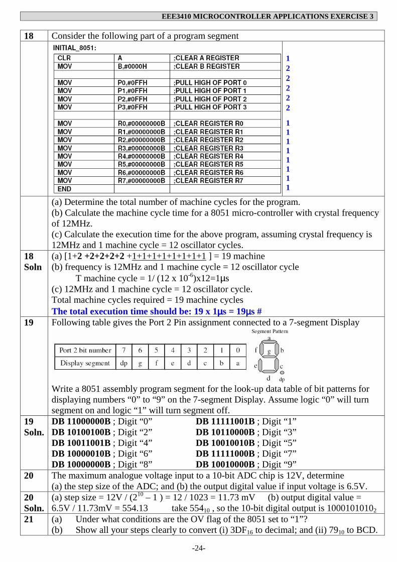
18 Consider the following part of a program segment
1 2 2 2 2 2
1 1 1 1 1 1 1 1
(a) Determine the total number of machine cycles for the program. (b) Calculate the machine cycle time for a 8051 micro-controller with crystal frequency of 12MHz. (c) Calculate the execution time for the above program, assuming crystal frequency is 12MHz and 1 machine cycle = 12 oscillator cycles.
18 Soln
(a) [1+2 +2+2+2+2 +1+1+1+1+1+1+1+1 ] = 19 machine (b) frequency is 12MHz and 1 machine cycle = 12 oscillator cycle T machine cycle = 1/ (12 x 10-6)x12=1µs (c) 12MHz and 1 machine cycle = 12 oscillator cycle. Total machine cycles required = 19 machine cycles The total execution time should be: 19 x 1µµµµs = 19µµµµs #
19 Following table gives the Port 2 Pin assignment connected to a 7-segment Display
Write a 8051 assembly program segment for the look-up data table of bit patterns for displaying numbers “0” to “9” on the 7-segment Display. Assume logic “0” will turn segment on and logic “1” will turn segment off.
19 Soln.
DB 11000000B ; Digit “0” DB 11111001B ; Digit “1” DB 10100100B ; Digit “2” DB 10110000B ; Digit “3” DB 10011001B ; Digit “4” DB 10010010B ; Digit “5” DB 10000010B ; Digit “6” DB 11111000B ; Digit “7” DB 10000000B ; Digit “8” DB 10010000B ; Digit “9”
20 The maximum analogue voltage input to a 10-bit ADC chip is 12V, determine (a) the step size of the ADC; and (b) the output digital value if input voltage is 6.5V.
20 Soln.
(a) step size = 12V / (210 – 1 ) = 12 / 1023 = 11.73 mV (b) output digital value = 6.5V / 11.73mV = 554.13 take 55410 , so the 10-bit digital output is 10001010102
21 (a) Under what conditions are the OV flag of the 8051 set to “1”? (b) Show all your steps clearly to convert (i) 3DF16 to decimal; and (ii) 7910 to BCD.

EEE3410 MICROCONTROLLER APPLICATIONS EXERCISE 3
-25-
(c) (i) Convert (-85)10 and (-49)10 into 8-bit 2’s complement form. (ii) Using 8-bit 2’s complement arithmetic to calculate (-85)10 - (49)10. (iii) Comment on the result you obtained in (c)(ii).
21 Soln.
(a) OV flag will be set to “1” when overflow or underflow occurs in signed arithmetic operation (b) (i) 3DF16 = 3x162 +13x161 + 15x160 =768+208+15 =99110 (ii) 7910 = 0111 1001 BCD (c) (i) 8510 = 0101 0101 1’s complement of (-85)10 = 1010 1010 2’s complement of (-85)10 = 1010 1011 4910 = 0011 0001 1’s complement of (-49)10 = 1100 1110 2’s complement of (-49)10 = 1100 1111 (ii) (-85) 1010 1011 + (-49) = 1100 1111 -134 1 0111 1010 (+122) (9th bit carry bit is not counted) (iii) The result is invalid because it shows that the addition of two negative numbers gets a positive answer. This exceeds the valid range of 8-bit 2’s complement representation so that Underflow occurs. Smaller than -128
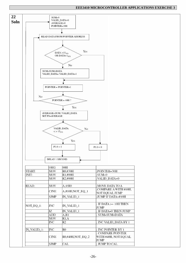
22 The temperature of a switch room is measured by 16 sensors distributed at different corners in the switch room. The sensors are connected to a 8051 microcontroller. The 16 temperature data, each is in length of 8 bits, will be automatically fetched to the internal memory location ranges from 30H - 3FH. The value of temperature data are bounded between 1(10) and 15(10). For the other numbers, it should be an error in the sensor and the data is invalid. The 8051 microcontroller should perform the following steps in sequence. Step 1: Check and sum up all valid temperature data from 30H to 3FH.
Discard all invalid data. Step 2: Dividing the sum by the total number of valid data to get the average
temperature value. (Use DIV instruction and the quotient after division is regarded as the average temperature value.)
Step 3 Output the average value to Port 0. Step 4 If invalid data is found in step 1, set P1.0 to “1”, otherwise set P1.0 to “0”. Step 5 Delay one second Step 6 Repeat steps 1 to 5 continuously.
(a) Draw a flow chart for this program design. (b) Write a 8051 assembly program for this program design. (You may assume that a 1-second delay subroutine, called DELAY, has been already in your program.)
EEE3410 MICROCONTROLLER APPLICATIONS EXERCISE 3
-26-
22 Soln

EEE3410 MICROCONTROLLER APPLICATIONS EXERCISE 3
-27-
23 An 8051 assembly time delay subroutine is given below:
DELAY: MOV R2, #6 DELA: MOV R3, #250 DELB: MOV R4, #200 DELC: DJNZ R4, DELC DJNZ R3, DELB DJNZ R2, DELA RET (a) (i) How many layers of Nested Loop are in this subroutine? (ii) How many cycles are in each loop? (b) How can the delay-time be doubled by modifying only a single instruction in the
subroutine? (c) If the clock frequency is 6 MHz, compute the execution times for each of the
following instructions: (i) MOV Rn, #data (ii) MOV A, Rn, (iii) DJNZ Rn, relative (iii) RET (d) Give one other method that can be used to generate time delay in 8051 without
the aid of external devices. 23 Soln
(a) (i) Three layers (ii) DELC Inner loop : 200 times DELB Middle loop : 250 times DELA Outer loop : 6 times (b) Make the delay-time double by modifying only a single instruction in the
subroutine. DELAY: MOV R2, #12 (c) 1 machine cycle = 12 clock cycles Machine Cycle Time = 12 / (6 x10⁶)=2µs

EEE3410 MICROCONTROLLER APPLICATIONS EXERCISE 3
-28-
(d) 8051 internal timer
24 (a) (b) (c)
The circuit shown in Fig. B4a converts the measured temperature from a thermister to a voltage that is inputted to a 8-bit ADC. The ADC has a conversion range of 0 – 5V. Fig B4b gives the resistance/temperature characteristics of the particular thermistor used in the circuit.
What is the temperature measured by the thermistor when the output of the A/D is 150 (decimal)? What is the maximum temperature that can be monitored by this circuit? The above circuit is used to monitor the temperature of a room. The output from the A/D converter is connected to the input Port 0 of a 8051 microcontroller and is constantly read by the microcontroller in each minute. Port 1 gives read/write signals to control the ADC and the respective connections are given in Table B4. If the room temperature exceeds 20oC, the microcontroller will send a signal ‘1’ to pin 1.3 to activate an alarm. Write a 8051 assembly language program that will perform the above task. (You may assume that a 1-minute delay subroutine, called DELAY, has been already in your program.)
Table B4 24 Soln (a)
When the output of the A/D is 150 (decimal), the reading of the thermistor is
From The RT / T curve, the reading of the thermistor is approx. 20oC.
(b) The maximum temperature that can be monitored with this circuit is obtained by: When temperature increases, Vo increases and RT decreases Vo(max) = 5 V and RT(min) = 1 kΩ From the curve, Tmax = 80oC
(c) WR EQU P1.0 INTR EQU P1.1 RD EQU P1.2 ORG 0H MOV P0,#0FFH
SUBB A,#151 JNC ALARM CLR P1.3 SJMP NEXT ALARM: SETB P1.3

EEE3410 MICROCONTROLLER APPLICATIONS EXERCISE 3
-29-
BACK: CLR WR SETB WR JB INTR,HERE CLR RD MOV A,P0
NEXT: ACALL DEL SETB RD SJMP BACK
Tut1 Q2
Convert the following numbers into decimal (a) 1100 1101(2)
= 1 x 27 +1 x 26 + 0 x 25 + 0 x 24 + 1 x 23 + 1 x 22 + 0 x 21 + 1 x 20 = 205(10) (b) 2746(8) = 2 x 83 + 7 x 82 + 4 x 81 + 6 x 80 = 1510(10) (c) 1524B(16) = 1 x 164 + 5 x 163 + 2 x 162 + 4 x 161 + 11 x 160 = 86603(10)
Tut1 Q6
What is the parity bit of the 8-bit code group below? (a) 11001101(2) Parity bit is : 1 for even parity ; 0 for odd parity (b) 11011101(2) Parity bit is : 0 for even parity ; 1 for odd parity
Tut1 Q1
Convert the following numbers into binary
(a) 456(10) = 1 1100 1000(2) 2000(10)=111 1101 0000(2)
(c) 1234(8) = 001 010 011 100(2) (d) 1524A(16) = 0001 0101 0010 0100 1010(2)

EEE3410 MICROCONTROLLER APPLICATIONS EXERCISE 3
-30-
Quiz Q2
(a) Perform the calculation with binary arithmetic (unsigned numbers) (i) 101101012 + 010000002 (ii) 110110012 −−−− 101010102
(iii) 000110112 x 0000 01112
(b) What is the smallest and largest number that can be represented by 8-bit 2’s complement format? Use 8-bit 2’s complement to calculate (-36)10 - 6710
(i) Sum = 10110101 + 01000000 = 11110101 (ii) Difference = 11011001 – 10101010=00101111 1101 1001 - 1010 1010 0010 1111 (iii) Product = 00011011 x 00000111=10111101
Range : -128 .. + 127 3610 = 0010 0100 2’s complement of (−36)10 = 1101 1100 6710 = 0100 0011 2’s complement of (−67)10 = 1011 1101 (−36) 1101 1100 + (−67) = + 1011 1101 −103 1 1001 1001 (-103) 10
Assg 1
1. Use a block diagram to show the components of a microprocessor system. Briefly describe the functions of these components.
2. State the differences between microprocessor and microcontroller. Refer to Lecture 1 – Powerpoint Slides 12-16