rf low pass filter design and fabrication using integrated
TRANSCRIPT
University of Central Florida University of Central Florida
STARS STARS
Electronic Theses and Dissertations, 2004-2019
2006
Rf Low Pass Filter Design And Fabrication Using Integrated Rf Low Pass Filter Design And Fabrication Using Integrated
Passive Device Technology Passive Device Technology
Heli Li University of Central Florida
Part of the Electrical and Computer Engineering Commons
Find similar works at: https://stars.library.ucf.edu/etd
University of Central Florida Libraries http://library.ucf.edu
This Masters Thesis (Open Access) is brought to you for free and open access by STARS. It has been accepted for
inclusion in Electronic Theses and Dissertations, 2004-2019 by an authorized administrator of STARS. For more
information, please contact [email protected].
STARS Citation STARS Citation Li, Heli, "Rf Low Pass Filter Design And Fabrication Using Integrated Passive Device Technology" (2006). Electronic Theses and Dissertations, 2004-2019. 957. https://stars.library.ucf.edu/etd/957

RF LOW PASS FILTER DESIGN AND FABRICATION USING INTEGRATED PASSIVE DEVICE TECHNOLOGY
by
HELI LI B.S., Zhejiang University, Hangzhou, China, 2003
A thesis submitted in partial fulfillment of the requirements for the degree of Master of Science
in the School of Electrical Engineering and Computer Science in the College of Engineering and Computer Science
at the University of Central Florida Orlando, Florida
Fall Term 2006

© 2006 Heli Li
ii

ABSTRACT
In this thesis, the whole process of design a low pass filter (LPF) for the wireless communication
application has been presented. Integrated passive device technology based on GaAs substrate
has been utilized to make the LPF. Schematic simulation and electromagnetic simulations are
extensively used in the design process. EM simulation is used in the selection of layout design
and processing parameters for design optimization of both the inductors and IPD harmonic filters.
The effective use of EM simulation enables us to realize the successful development of high
performance harmonic filters.
To make the optimization be more flexible and also for a deeper understanding of the
optimization theory, optimization using genetic algorithm is also implemented. The weight of
each targets are adjustable, and a non-uniformly distributed goal for the harmonic rejection range
is introduced to achieve better optimization results.
The embedded LPF is built and measurement results show good agreement with the simulation
data. This kind of very compact, high performance harmonic filters can be used in radio
transceiver front-end modules. The realized harmonic filters have insertion loss less than 0.6 dB
and harmonic rejections greater than 25 dB with a compact die size of 0.8 mm2.
iii

ACKNOWLEDGMENTS
I would like to express my gratitude to my advisor Dr. Thomas X. Wu , for his guidance, advice
and patience throughout this work. He is the best advisor and teacher I could have wished for. I
am grateful for the opportunity to work with him.
I would also like to thanks people from TriQuint. Kamran Cheema gave me this opportunity and
management support to work with this project. Many people have been involved in this work
also. Xiaomin Yang, Nicolas Layus, Arjun Ravindran, Riad Mahbub gave me a lot of technical
support during this work. Without their expertise and additional comments, this work would not
be so smooth.
I would also like to thanks Dr. W. Linwood Jones, for his support as my committee member.
Finally, I would like to express my gratitude to my family. My husband gives me all his support
to help me to overcome the difficulties. My parents always encourage me and guide me,
supported each of my decision and advised me from time to time.
iv

TABLE OF CONTENTS
LIST OF FIGURES ...................................................................................................................... vii
LIST OF TABLES......................................................................................................................... ix
CHAPTER ONE: INTRODUCTION............................................................................................. 1
1.1 Filter Integration ................................................................................................................... 1
1.2 Basic Filter Types ................................................................................................................. 3
1.3 Harmonic Filters ................................................................................................................... 5
1.4 Organization of Thesis.......................................................................................................... 6
CHAPTER TWO: TOPOLOGY AND SCHEMATIC DESIGN ................................................... 7
2.1 LPF Specification.................................................................................................................. 7
2.2 LPF Topology ....................................................................................................................... 9
2.3 Optimization in ADS .......................................................................................................... 13
2.4 Bondwire Sensitivity........................................................................................................... 15
CHAPTER THREE: OPTIMIZATION USING GENETIC ALGORITHMS ............................. 18
3.1 Optimization Based on Genetic Algorithms (GA).............................................................. 18
3.2 Flow Chart of GA ............................................................................................................... 19
3.2.1 Selecting the Variables and the Cost Function ............................................................ 21
3.2.2 Selection, Mating and Mutation................................................................................... 25
v

3.3 GA Optimization Results.................................................................................................... 25
CHAPTER FOUR: ON CHIP INDUCTOR DESIGN ................................................................. 27
4.1 Spiral Inductor Modeling.................................................................................................... 27
4.1.1 Inductance .................................................................................................................... 28
4.1.2 Series Resistance.......................................................................................................... 29
4.1.3 Parasitic Capacitance ................................................................................................... 30
4.1.4 Quality Factor .............................................................................................................. 30
4.2 Inductor Design................................................................................................................... 30
4.2.1 Two Port Network Models of Inductor........................................................................ 32
4.2.2 Designed Inductor........................................................................................................ 35
CHAPTER FIVE: 3D ELECTROMAGNETIC MODELING..................................................... 38
5.1 Coupling Effect in Real Circuit .......................................................................................... 38
5.2 3D Electromagnetic Simulation.......................................................................................... 39
CHAPTER SIX: LAYOUT AND FABRICATION..................................................................... 44
6.1 Advantage of GaAs Substrate............................................................................................. 44
6.2 TriQuint TQRLC Technology ............................................................................................ 45
6.3 LPF Test Result................................................................................................................... 48
CHAPTER SEVEN: CONCLUSION........................................................................................... 52
LIST OF REFERENCES.............................................................................................................. 54
vi
LIST OF FIGURES
Figure 1 A block diagram of the front-end module ....................................................................... 3
Figure 2 General filter response (a) Low pass (b) High pass (c) Band pass (d) Band stop........... 4
Figure 3 The fundamental frequency and the harmonic frequencies............................................. 5
Figure 4 Circuit topology of the LPF........................................................................................... 10
Figure 5 Circuit topology of the LPF with Bondwires. ............................................................... 11
Figure 6 3D model of the wirebond connection .......................................................................... 12
Figure 7 Electrical performance with the optimized lumped elements in ADS .......................... 15
Figure 8 Flowchart of a binary GA [10] ...................................................................................... 20
Figure 9 Optimization target........................................................................................................ 22
Figure 10 Optimization goal for the harmonics rejection range .................................................. 23
Figure 11 S21 optimization results by genetic algorithm ............................................................ 26
Figure 12 Top view of a spiral inductor....................................................................................... 28
Figure 13 3D view of inductor on the substrate with in parasitic capacitance highlighted. ........ 31
Figure 14 A practical inductor model .......................................................................................... 32
Figure 15 Electrical parameters of L1 ......................................................................................... 36
Figure 16 Electrical parameters of L2 ......................................................................................... 37
Figure 17 3D modeling of LPF in the HFSS ............................................................................... 40
Figure 18 Interface of the HFSS simulation result connected into ADS..................................... 41
vii

Figure 19 3D simulation results compare with circuit level simulation results........................... 42
Figure 20 Optimized 3D simulation results ................................................................................. 43
Figure 21 Cross section of Triquint’s TQRLC process technology ............................................ 46
Figure 22 Fabricated Low Pass Filter .......................................................................................... 48
Figure 23 Test environment setup and simulation....................................................................... 49
Figure 24 Electrical performance of realized LPF....................................................................... 50
viii

LIST OF TABLES
Table 1 Design specification of LPF for GSM/AMPS application ............................................... 9
Table 2 Optimized value based on ADS simulation.................................................................... 14
Table 3 The sensitivity of bondwire inductance to the goals....................................................... 17
Table 4 The lumped element optimization using genetic algorithms .......................................... 26
Table 5 Inductor geometric parameters ....................................................................................... 35
Table 6 Selected Properties of GaAs and Silicon ........................................................................ 45
Table 7 TQRLC process details................................................................................................... 47
Table 8 Measurement results for the realized LPF ...................................................................... 51
ix

CHAPTER ONE: INTRODUCTION
Wireless communication has become increasingly important in the past several years. Despite
this increase in complexity, both the size and cost of handsets have continued to decline
significantly. This has been achieved by increasing levels of integration. Since the cellular
phones are designed to meet the multi-band application instead of single band nowadays, highly
integrated front-end modules are designed for this kind of purposes, which include filters and
switch in a single module. For the size and cost limitation, high level of integration for filters are
required.
1.1 Filter Integration
The trend of system’s size and cost reduction requires the filters to be integrated in the module.
There are some obvious advantages if the filters can be integrated. While discrete filters take a
large portion of printed circuit board space and increase the transceiver’s overall size, size can be
reduced by integrating filters on RF modules. Besides the size reduction, the cost of the RF
receiver can also be reduced because fewer external components will be required. Moreover,
module solution provides the RF signal with the opportunity to travel on chip, so that the power
1

dissipation will be reduced. For the traditional one with discrete filter, RF signals need to travel
off-chip through package pins to an external filter on the printed circuit board, which introduces
the power loss [1].
Multi-chip module (MCM) is one of the solutions to do the integration. It is a structure
consisting of two or more integrated circuits electrically connected to a common circuit base and
interconnected by conductors in the base. MCM has more flexibility to tailor its characteristics to
meet the needs of a specific RF chipset. In addition, it is much easier, faster, and cheaper, to add
new functionality to a multi-chip solution than to a single dedicated die solution [2].
One filter integration application is used for the design of front-end module (FEM), which
integrates the switching and transmits LPF function, as well as SAW filters. Figure 1 is a block
diagram of a FEM. This kind of dual-band FEM contains a SP3T (single pole three throw)
switch, diplexer, two integrated LPFs and two SAW filters. Signals come from the antenna to the
SP3T switch, then to the diplexer where GSM900 and DCS 1800 are separated, and then to the
two saw filters respectively. At the Tx path, the amplified signals travel through the LPF and
transmitted to the antenna.
The whole FEM module is in a scale of several millimeters. To achieve cost and size reduction,
high performance passive process technology for integrated passive devices (IPD) are used for
the LPF fabrication. The small size LPF based on IPD technology are widely utilized in hand-
2

held RF module and system requiring low cost solution and strict volumetric efficiency, such as
front end module.
Switch
Diplexer
LPF
LPF
SAW filter
DCS 1800 Rx
GSM 900 Rx
DCS 1800 Tx
GSM 900 Tx
Antenna
Figure 1 A block diagram of the front-end module
1.2 Basic Filter Types
Filters are essential to the operation of most electronic circuits. In circuit theory, a filter is an
electrical network that alters the amplitude and/or phase characteristics of a signal with respect to
frequency. Ideally, a filter will not add new frequencies to the input signal, nor will it change the
component frequencies of that signal, but it will change the relative amplitudes of the various
frequency components and/or their phase relationships. Filters are often used in electronic
systems to emphasize signals in certain frequency ranges and reject signals in other frequency
ranges. Such a filter has a gain which is dependent on signal frequency [3]. Based on the
3

frequency domain responses, there are four filter types, named as low pass filter, high pass filter,
band pass filter and band stop filter. Low pass filters (LPF) allow low frequencies to pass while
rejecting the high frequencies which are higher than the cut off frequency. High pass filters have
the opposite function to that of LPF. They allow the frequency above the cut off to pass with the
minimal loss, and reject the signal in the low frequency. Band pass filters have upper and lower
cut-off frequencies. The upper cut-off frequency determines the maximum frequency passed,
while the lower cut-off frequency decides the minimum frequency to be passed. Band stop filters
are the opposite to band pass designs. Figure 2 illustrate those kinds of filter types.
Figure 2 General filter response (a) Low pass (b) High pass (c) Band pass (d) Band stop
Frequency (b)
Frequency
Output Level Output Level
(a)
Frequency (d)
Output Level
Frequency(c)
Output Level
4

1.3 Harmonic Filters
When signals are transmitted in the system, there are harmonic currents and voltages occurred,
which means the currents and voltages that are continuous multiples of the fundamental
equency. Because harmonic currents provide power that cannot be used and also takes up fr
electrical system capacity, they can lead to malfunctioning of the system, and result in downtime
and increase in operating costs. For the improvement of the whole system, a harmonic filter is
used to eliminate the harmonic distortion caused by appliances [4]. Figure 4 is the example of
harmonic frequencies which accompany the fundamental frequency.
Figure 3 The fundamental frequency and the harmonic frequencies
5

Harmonic Filte onic filter is
built using an array of capacitors, inductors, and resistors. There are two ways to eliminate the
harmonics, one is to take the form of a simple line reactor, and another way is to use a series of
parallel resonant filters. If the filter is placed in series with the load and uses parallel components,
i.e., inductors and capacitors are in parallel, this filter is a current rejecter. If the filter is placed in
parallel with the load and its components are built in series. This filter is a current acceptor.
1.4 Organization of Thesis
rs can be made in a passive way or in an active way. A passive harm
This thesis discusses the design ated filter design, including the
characterization, design and fabrication of RF LPF using TQRLC technology on GaAs substrate.
resents the Genetic Algorithm method for optimization. Chapter 4 introduces the on-chip spiral
inductors design with HFSS. Chapter 5 is the 3D simulation procedure and result for the whole
LPF. In Chapter 6, the realized filter and its measurement results are presented. And Chapter 7 is
the conclusion.
procedure of on chip integr
Chapter 2 is focused on the topology and schematic design based on ADS simulation. Chapter 3
p
6

CHAPTER TWO: TOPOLOGY AND SCHEMATIC DESIGN
very circuit design comes from topology determination and schematic design. With circuit
2.1 LPF Specification
E
topology determination, a circuit level simulation and optimization based on the specification
need to be performed. Schematic design establishes the general scope, conceptual design, scale
and relationships among the components of the LPF.
he LPF was built to cover the GSM/AMPS band from 824 MHz to 915 MHz, which can cover
SM represent for the Global System for Mobile Communication. GSM-850 is used in the
T
the Tx band for GSM850, GSM900 and AMPS band.
G
United States, Canada and many other countries in the America. To send information from the
mobile station to the base transceiver station, frequency range from 824 MHz to 849 MHz is
used. Similarly, GSM-900 is used in most other parts of the world. It uses the frequency range
from 890 MHz to 915 MHz to send information from the mobile station to the base transceiver
7

station. Except for this band of primary GSM (P-GSM), there is also Extended GSM (E-GSM)
with Tx frequency range of 880 MHz to 915 MHz and Railways GSM (R-GSM) working at
frequency form 876 MHz to 915 MHz.
The frequency band for Advanced Mobile Phone System (AMPS) is also covered. AMPS is one
he specification of the LPF to be designed is listed in Table 1.There are several performance
of the earliest commercial cellular systems. The frequencies allocated to AMPS by the FCC
range between 824 to 849 MHz for mobile to base and 869 to 894 MHz for base to mobile.
AMPS technology is currently deployed throughout North America and AMPS-derivative
systems are deployed in a majority of worldwide cellular markets.
T
specifications used to represent a filter, including insertion loss, attenuation, return loss, ripple,
etc. Insertion loss is the total RF transmission loss resulting from the inserting of a device in a
transmission line. And it is the ratio of signal power at the output of the inserted device to the
signal power at its input. Attenuation is the reduction in amplitude and intensity of a signal in the
stop band. Attenuation in the frequency range of twice the passband is also called 2nd harmonic
rejection. For the frequency range at three times of the passband, it is referred to as 3rd harmonic
rejection. Return loss express the ratio at the junction of input port, of the amplitude of the
reflected wave to the amplitude of the incident wave.
8

To design a harmonic rejection low-pass filter suitable for the application in the transmit pass of
the front-end module, the insertion loss is required for less than 0.6 dB and the out of band
rejection in the 2nd and 3rd harmonic frequency range is required to be more than 25 dB.
Table 1 Design specification of LPF for GSM/AMPS application
Parameter Frequency Range (MHz) Requirement Insertion Loss 824 - 915 0.6 dB max Return Loss 824 - 915 20 dB min Attenuation 1648 - 1830 25 dB min Attenuation 2472 - 2745 25 dB min
2.2 LPF Topology
Advanced Design System (ADS) is an electronic design automatic software system and it is used
in our filter design. Figure 5 below shows the filter circuit topology. This five-element filter
includes two embedded inductors and three capacitors. The inductor and capacitor pairs are
designed for the harmonic rejection purpose.
Filter of this kind of topology can achieve high rejection at 2nd and 3rd harmonic frequencies and
can hence be used for harmonic suppression in the FEM after power amplifier. The LC resonator
L1/C1 and L2/C2 suppress the 3rd and 2nd harmonics, respectively. C3 functions as a blocking
9

capacitor, with the help the bondwire inductance, C3 and the bondwire can perform as another
resonator.
PortP1Num=1
PortP2Num=2
CAPQC3CAPQ
C1
INDQL1
PortP3Num=3
CAPQC2
INDQL2
Figure 4 Circuit topology of the LPF
When the LPF is combined in the module, there are bondwires used to connect the input and
output pads with other ports. Bondwires are the dominant technique to connect an RFIC to the
package, even though they have large self and mutual inductances. They are able to tolerate die
thermal expansion and placement uncertainty. However, their inductance creates significant
challenges for RFIC design, as well as some opportunities [6].
10

Because bondwires are made using gold with a diameter of 1 mil, there inductance cannot be
neglected. It’s necessary to include the bondwire in the ADS schematic simulation. Figure 6
includes the bondwire inductance when the LPF is used in the module, where L_in, L_out and
L_GND represent for the wire bond inductance.
INDQL_out
INDQL2
CAPQC2
INDQL_GND
CAPQC3
INDQL_in
CAPQC1
INDQL1
TermTerm1
Z=50 OhmNum=1
TermTerm2
Z=50 OhmNum=2
L_in L_out
L_GND
Figure 5 Circuit topology of the LPF with Bondwires.
The bondwire inductance is dependent on the length of the wire bond and the cross section area.
The inductance and mutual inductance can be calculated using the Eq. (3.1) for straight wires [7],
[8]
0 2[ln( 0.75)]2
l lLr
μπ⋅
≈ ⋅ − (2.1)
11

where 0μ is the permeability in free space, l is the wire length, and r is the radius of the wire.
The dominant technology in the industry nowadays is using the bondwire with the diameter of 1
mil. For the bondwire with 2 mm long, the formula can yield 2 nH for the inductance. So
industry people estimate the inductor value of the bondwire by 1 nH/mm [9].
As long as the chip positions are fixed, the wire bond lengths are known. Except for the
estimation based on the previous relationship, it is preferred to perform some HFSS simulation to
simulate the inductance values for bondwires. Figure 7 shows the bondwire model in the HFSS
simulation. The bondwire is used to connect one chip to another. GaAs substrate and BCB are set
exactly as the thickness in the real chips.
Bondwire
Pad
GaAs
BCB
Figure 6 3D model of the wirebond connection
12

After the simulation, we found that the inductance of the wire bond is approximately performed
as 1 nH/mm at the 1 GHz, and the resistance is around 0.1 Ohm although it is also length
dependent. To make things easier, we use the estimated value calculated with the relationship
mention above.
In this design, the length of the wire bond connect to the input of LPF is 1.1 mm. For this one,
we use an inductor with inductance of 1.1 nH and resistance of 0.1 Ohm to simulate in the circuit.
Accordingly, the other two bondwires named as L_out and L_GND. We use 0.6 nH and 0.1 Ohm
for both of them because they have the same length.
2.3 Optimization in ADS
After the circuit topology is determined, a circuit level simulation and optimization based on the
specification including insertion loss and out-of-band rejection need to be conducted. There is an
optimization tool available in the ADS, making it convenient to set up the optimization goals and
then optimize the lumped elements. Here, the task is to design an LPF with the insertion loss less
than 0.6 dB at 824 MHz to 915 MHz, and the out of band rejection in the 2nd and 3rd harmonic
frequency range more than 25 dB. Usually the goals should be set more strictly than the
specification to get good optimization.
13
The bondwire cannot be optimized because it is position dependent. When the position of the
LPF is fixed, there is little room for the change of bondwire. However, there are two inductors
named L1, L2 and three capacitors named C1, C2 and C3 that can be optimized to let the circuit
perform well as the specifications are required. The values after optimization have been shown in
Table 2.
Table 2 Optimized value based on ADS simulation
Unit Value L1 nH 5.05 L2 nH 4.6 C1 pF 0.76 C2 pF 1.89 C3 pF 2.91
L2 and C2 are used for the 2nd harmonic rejection, while L1 and C1 are for the 3rd harmonic
rejection. The simulation results are shown in Figure 8. The realized insertion loss is less than
0.5 dB. Rejection of 2nd harmonic is greater than 25 dB, and the rejection of 3rd harmonic is
greater than 32 dB.
14
0.8 1.0 1.2 1.4 1.6 1.8 2.0 2.2 2.4 2.6 2.8 3.0 3.2 3.4 3.6 3.80.6 4.0
-45
-40
-35
-30
-25
-20
-15
-10
-5
-50
0
freq, GHz
dB(S
(2,1
))m1m2
m3 m4
m5
m6
dB(S
(1,1
))
m1freq=dB(S(2,1))=-0.367
824.0MHz
m2freq=dB(S(2,1))=-0.427
915.0MHz
m3freq=dB(S(2,1))=-26.175
1.648GHz
m4freq=dB(S(2,1))=-25.947
1.830GHz
m5freq=dB(S(2,1))=-36.018
2.472GHz
m6freq=dB(S(2,1))=-32.805
2.745GHz
Figure 7 Electrical performance with the optimized lumped elements in ADS
2.4 Bondwire Sensitivity
Although we know that the bondwires can influence the whole circuit performance, and they
have to be simulated at the beginning of the circuit design. However, we don't want the circuit to
be too sensitive with the bondwire length, unless the bondwire is initially designed with the
purpose of substituting certain inductor. For our design, since the LPF is designed to embedded
in a module, it’s better to let the circuit be stable, which means that the circuit is less dependent
on the bondwire. So that the LPF is less position dependent, and can be utilized more flexibly.
15

In order to know how the parameters in the device model affect the whole circuit performance,
we perform the sensitivity analysis for each bondwire. Sensitivity analysis is a fundamental
element of gradient optimization methods. Sensitivity analysis comprises a single-point or
infinitesimal sensitivity analysis of a design variable. For circuit design, it involves taking partial
derivatives of the response with respect to a design variable of interest. It is thought that these
numbers can help pinpoint variables that contribute disproportionately to performance variance.
Sensitivities are approximated as follows:
0
0
( ) ( ) ( )i
i ip
i i i
iR P R P R PSP P P
αα
+
+
−= =
− (2.2)
where is the response evaluated at the nominal point and is the response due to a
perturbation in the ith parameter.
)( 0PR )( +PR
Normalized sensitivities use the approximate gradient (single-point sensitivity) to predict the
percentage change in the response due to a 1% change in the design variable. Normalized
sensitivity is defined as
0 0 0 0 0[( ) /( ( ))] {[ ( ) ( )] /( ( ))}/{[ ] / }i
iN i P i i i i i i iS P S P R P R P R P R P P P P+ +− = = − − 0
(2.3)
The sensitivity of the bondwire has been analyzed, and the sensitivity is shown in Table 3.
16

Table 3 The sensitivity of bondwire inductance to the goals
Optimization Goal L_in L_out L_GND insertion loss less than 0.5 dB 0.082 0.027 -0.036 2nd harmonic rejection larger than 25 dB 0.033 -0.006 0.109 3rd harmonic rejection larger than 25 dB -0.008 -0.026 0.256
In the insertion loss point of view, the bondwire connected from the input pad to the module
plays a more important role compared with other two bondwires. While consider the harmonic
rejection, the L_GND is more sensitive. This gives the engineers with the idea that L_GND
needs to be bonded in the module carefully to yield a good performance.
17

CHAPTER THREE: OPTIMIZATION USING GENETIC ALGORITHMS
Optimization is the process of making things better. ADS provides with us a tool to optimize
directly by choosing the optimization goal and optimization type. That is a convenience way to
make things done quickly. However, it’s a black box and we don't know the detail in the code.
Writing our own optimization code can make the optimization be more flexible. There are many
types of optimization methods, like random, gradient, Newton, etc. Genetic algorithm is chosen
for its advantage of producing stunning results when traditional optimization approaches fail
sometimes.
3.1 Optimization Based on Genetic Algorithms (GA)
Genetic algorithms were formally introduced in the 1970s by John Holland at University of
Michigan. It is an optimization and search technique based on the principles of genetics and
natural selection which allows a population composed of many individuals to evolve under
specified selection rules to a state that maximizes the fitness. Genetic algorithms are a particular
class of evolutionary algorithms that use techniques inspired by evolutionary biology such as
18

inheritance, mutation, selection, and crossover (also called recombination). Some of the
advantages of a GA include that it [10]
Optimizes with continuous or discrete variables
Doesn’t require deviation information
Simultaneously searches from a wide sampling of the cost surface
Deals with a large number of variables
Is well suited for parallel computers
Optimizes variables with extremely complex cost surface
Provides a list of optimum variables, not just a single solution
May encode the variables so that the optimization is done with the encoded variables and
Works with numerically generated data, experimental data, or analytical functions.
3.2 Flow Chart of GA
The GA begins by defining the optimization variables, the cost function, and the cost. It ends by
testing for convergence. In between, a path through the components of the GA is shown as a
flowchart in Figure 9.
19

Define cost function, cost, and variables Select GA parameters
Generate initial population
Decode chromosomes
Find cost for each chromosome
Select mates
Mating
Mutation
Convergence check
Done
Figure 8 Flowchart of a binary GA [10]
20
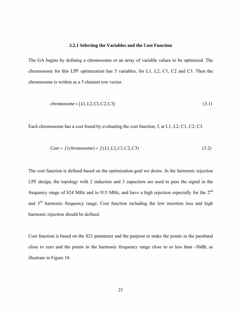
3.2.1 Selecting the Variables and the Cost Function
The GA begins by defining a chromosome or an array of variable values to be optimized. The
chromosome for this LPF optimization has 5 variables, for L1, L2, C1, C2 and C3. Then the
chromosome is written as a 5 element row vector.
[ 1, 2, 1, 2, 3]chromosome L L C C C= (3.1)
Each chromosome has a cost found by evaluating the cost function, f, at L1, L2, C1, C2, C3.
( ) ( 1, 2, 1,Cost f chromosome f L L C C C= = 2, 3) (3.2)
The cost function is defined based on the optimization goal we desire. In the harmonic rejection
LPF design, the topology with 2 inductors and 3 capacitors are used to pass the signal in the
frequency range of 824 MHz and to 915 MHz, and have a high rejection especially for the 2nd
and 3rd harmonic frequency range. Cost function including the low insertion loss and high
harmonic rejection should be defined.
Cost function is based on the S21 parameter and the purpose to make the points in the passband
close to zero and the points in the harmonic frequency range close to or less than -30dB, as
illustrate in Figure 10.
21

Passband
2nd harmonic 3rd harmonic
Figure 9 Optimization target
N points evenly distributed in pass band have been chosen. Each point has a value. For the
representation of S21 in the passband close to zero, it is defined in the cost function as the sum of
those n values equals to zero.
1_ 2
N
Cost PB S n=∑ 1( ) (3.3)
22

For the representation of S21 in the harmonic frequency band less than -30 dB, the cost cannot
simply add those S21 values together, since the S21 in the harmonic frequency range is not
uniformly distributed. It’s necessary to use the sum of the difference between S21 and some
target rejection value.
Figure 11 shows an enlarged harmonic frequency range of Figure 10. It shows that the lowest
S21 in harmonic frequency range can be obtained approximately in the middle of the each
frequency range. And the highest S21 is happened at the left and right edges of each rejection
band. With this feature, an adjusted goal has been made, to fit the S21 in the middle deeper than
what they are in the left and right edges, as shown in Figure 11.
Estimated real performance
Optimization Goals
Harmonic frequency range
Upper goal
Lower goal
Upper goal
Left edge Right edge
Middle
Figure 10 Optimization goal for the harmonics rejection range
23

If we choose M points for the rejection band, m for each point, the points’ values in the dash line
can be expressed as
2( _ _ )( ) _2M upper goal lower goalG m lower goal m
M−
= + − ⋅ (3.4)
The cost of those M points in the harmonic rejection band can be described as
1_ ( 21( ) (
M
Cost HR S m G m= −∑ ))
_ 3
(3.5)
The total cost is the combination of the cost in the passband and the cost in the 2nd and 3rd
harmonic rejection band. So the total cost is
_ _ _ 2Cost total Cost PB Cost HR Cost HRα β γ= ⋅ + ⋅ + ⋅ (3.6)
Here, represent the cost for the 2_ 2Cost HR nd harmonic rejection, while stand for
the cost in the 3
_ 3Cost HR
rd harmonic rejection region. achieves to zero when specification is
met. And
_Cost total
α , β and γ are for the weight change. They are adjustable according to the importance
of the application.
24

3.2.2 Selection, Mating and Mutation
The chromosomes are first selected randomly by the computer. Those who have lower costs will
survive while those with higher costs are discarded. The selection rate can be adjusted, and is the
fraction of the population that survives for the next step of mating.
Then two chromosomes are selected from the mating pools of survivors to produce two new
offspring. After the parents have been chosen, a crossover point is randomly selected between
the first and last bit of the parents’ chromosomes. And the four parts from the parents switch
with each other internally. Those offspring are born to replace the discarded chromosomes.
Mutation is the second way of GA explores a cost surface. It can introduce traits not in the
original populations and keeps the GA from converging too fast before sampling the entire cost
surface. Simple point mutation changes from a 1 to a 0 or a 0 to a 1 have been chosen in our GA.
3.3 GA Optimization Results
Figure 12 is the optimization results using GA in MATLAB. The optimized value for L1, L2, C1,
C2, C3 are listed in Table 4. The insertion loss is less than 0.41 dB, harmonic rejection is more
than 30 dB for both 2nd and 3rd harmonic rejection band.
25
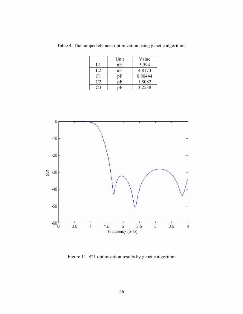
Table 4 The lumped element optimization using genetic algorithms
Unit Value L1 nH 5.594 L2 nH 4.8173 C1 pF 0.80444 C2 pF 1.8082 C3 pF 3.2538
Figure 11 S21 optimization results by genetic algorithm
26

CHAPTER FOUR: ON CHIP INDUCTOR DESIGN
During the past decade, there is emergence of the portable and low cost consumer applications.
Inductor is one of the most important circuit elements, especially for RF application. It can be
not only used for filtering RF signals, but also included in low noise amplifiers, oscillators, etc.
For low frequency applications, passive devices can be connected externally, but as frequency
increases, the characteristics of the passive device would be overwhelmed by parasitic effects
[11]. As a result, on chip passive components are commonly used in RF applications. The spiral
inductor has established itself as a standard passive component in RF chip design. There is a
great incentive to design, optimize and model spiral inductors.
4.1 Spiral Inductor Modeling
Spiral inductors are implemented in the integrated circuits by winding metal lines into spiral on a
planar surface as shown in Figure 13. Although there are other shapes of spiral inductors used
for particular purpose, a rectangular shaped inductor is the most traditional and classic one. The
parameters of a rectangular inductor to describe its geometry are outer dimension as L1 and L2,
number of turns, width and space.
27

W S
L2
L1
Figure 12 Top view of a spiral inductor
4.1.1 Inductance
Inductance is the most important parameter to describe an inductor. It is an effect which results
from the magnetic field that forms around a current carrying conductor. The magnetic flux is
proportional to the current when electric current goes through the conductor. Current change will
create a change in the magnetic flux and in turn generate an electromotive force that acts to
28

oppose this change in current. The larger the generated electromotive force is for a unit change in
current, the larger the inductance.
4.1.2 Series Resistance
No inductor is perfect. There are losses in the inductor. The losses cannot be neglected since they
can affect the whole circuit performance. In this case, series resistance is another major
parameter to be considered.
The series resistance is the combination of the metal loss and the eddy current effect. Due to the
finite conductivity of the metal trace, there is metal loss. When frequency increases, the current
density becomes non-uniform and conductor is subjected to time varying magnetic fields. This
introduces the formation of eddy current. Eddy current manifests itself as skin and proximity
effects, and produces its own magnetic fields to oppose the original field. It can be either induced
by the time varying current flow in itself, or by the time varying current produced by a nearby
conductor. Eddy currents reduce the net current flow in the conductor and hence increase the ac
resistance. Because spiral inductors being used are based on a multi-conductor structure, eddy
currents are caused by both proximity and skin effects [12].
29

4.1.3 Parasitic Capacitance
Figure 14 shows a 3D view of an inductor modeled in a substrate with mold on it. When
inductors are used on the RF chips, they are fabricated on the substrate. The bulk substrate can
be made of different materials like Si or GaAs. This introduces the parasitic capacitances.
4.1.4 Quality Factor
The quality factor describes how good an inductor can work as an energy-storage element. The
most fundamental definition for Q is defined as energy stored over the energy lost, as listed in Eq.
(4.1). Because the only desirable source of storage energy is magnetic field and hence any source
of storing electric energy such as capacitances is considered as a parasitic.
__
Energy StoredQEnergy Loss
= ( 4.1)
4.2 Inductor Design
There are some empirical formulas based on experimental results for the inductance and Q value
estimation. However, due to the dramatic improvement of the computer speed, people now tend
to use numerical simulators to calculate the electromagnetic field distribution and then extract
30

the parameters like inductance and quality factor. Simulation tools like ADS momentum, IE3D,
sonnet and HFSS are popular software being used recently. We choose HFSS for its 3D full
wave calculation characteristic.
The inductor model set in the HFSS is shown in Figure 14. HFSS will calculate it as a two port
network and the inductance, resistance and quality factor values can be extracted according to
that.
GaAs
BCB
Mold
Inductor
Figure 13 3D view of inductor on the substrate with in parasitic capacitance highlighted.
31
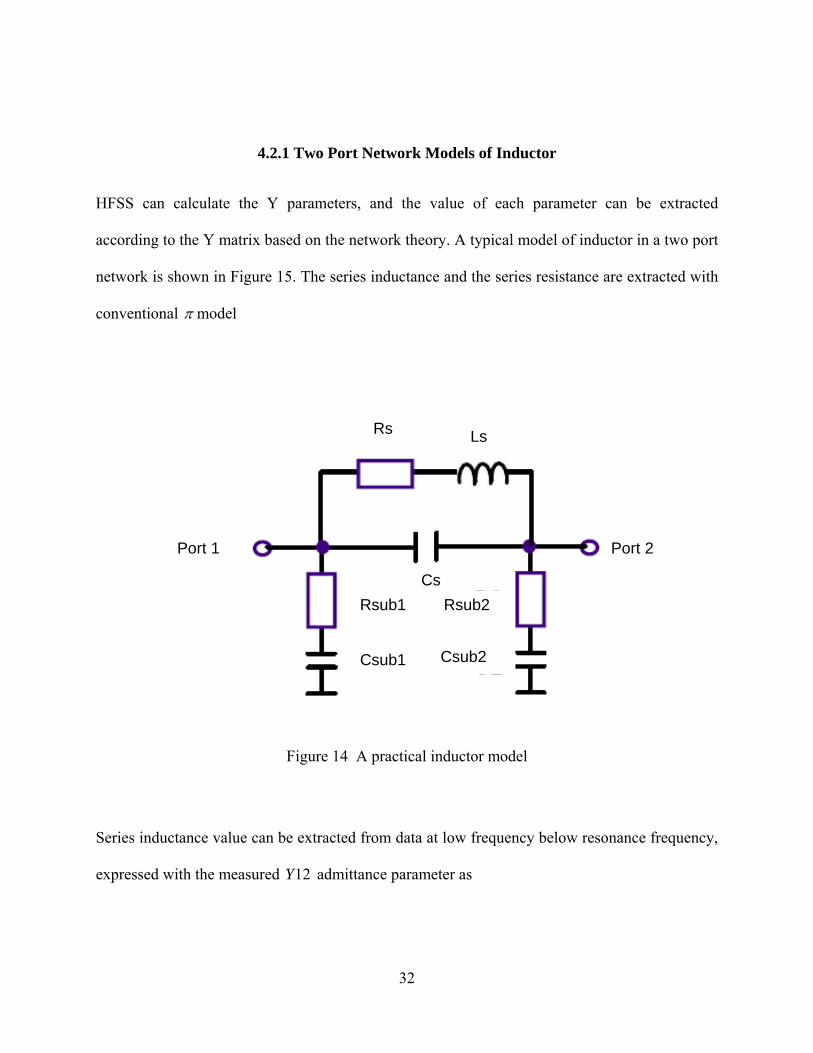
4.2.1 Two Port Network Models of Inductor
HFSS can calculate the Y parameters, and the value of each parameter can be extracted
according to the Y matrix based on the network theory. A typical model of inductor in a two port
network is shown in Figure 15. The series inductance and the series resistance are extracted with
conventional π model
Port 1 Port 2
Rs Ls Rs
Cs Rsub1 Rsub2
Csub1 Csub2
Figure 14 A practical inductor model
Series inductance value can be extracted from data at low frequency below resonance frequency,
expressed with the measured admittance parameter as 12Y
32

112 212 (
2
Ls Y Yfreq imagπ=
+⋅ ⋅ )
. (4.2)
Parasitic capacitanceCs and series resistance Rs are crucial factors for the inductor performance
and quality factor. Parasitic capacitance from metal trace can be extracted from the high
frequency data as
122 (
12 21
Csfreq imag
Y Yπ
=⋅ ⋅
+)
. (4.3)
Series resistance can be obtained using
2(12 21
Rs realY Y
)−=
+ (4.4)
by extracting data at low frequencies before resonance frequency.
Substrate parameters can also been extracted from the conventional π model. For substrate loss
calculation,
11( 12 2111 ( )
2
subR real Y YY=
++
) (4.5)
33

For parasitic capacitances, they are extracted from the high frequency data, using the following
equations as
11
12 ( 12 2111 ( )2
subCfreq imag Y YY
π )
−=
⋅ ⋅+
+
. (4.6)
2subR and 2subC can be obtained similarly by symmetry property.
The quality factor is defined as the energy stored over energy lost, and it can be expressed as
1( )111( )11
imYQ
reY
= (4.7)
Those equations can be used to extract the parameters directly from the Y matrix. Instead of
outputting Y matrix directly, some software can only output the S parameter. In this case, a
conversion from S matrix to Y matrix needs to be done.
34

4.2.2 Designed Inductor
The die size of the LPF is 1.15 mm in length and 0.7 mm in width, including two inductors and
necessary traces. With the help of HFSS, the two inductors for the replacement of L1 and L2 in
the circuit topology have been designed. With the size limitation considered together, the two
inductors have scales listed below. N, W and S represent the number of terns, the metal width,
and the conductor spacing, respectively.
Table 5 Inductor geometric parameters
Inductor Area (μm2) N W (μm) S(μm) L1 310x310 3.25 10 8 L2 330x330 3.25 10 8
HFSS simulation provides the two port simulation results. To get the inductance, series
resistance and quality factor, an additional parameter extraction is conducted. Electrical
parameters for the two inductors are listed in Figure 16 and Figure 17. L1 has a quality factor
better than 23, and L2 has a quality factor better than 22.
35

1.0 1.5 2.0 2.5 3.0 3.5 4.0 4.50.5 5.0
6.0E-9
8.0E-9
1.0E-8
1.2E-8
4.0E-9
1.4E-8
freq, GHz
L
m1
m1freq=L=5.053E-9
850.0MHz
0.2
0.4
0.6
0.8
0.0
1.0
1.0 1.5 2.0 2.5 3.0 3.5 4.0 4.50.5 5.0
freq, GHz
R
m2
m2freq=R=0.023
850.0MHz
15
20
25
30
10
35
1.0 1.5 2.0 2.5 3.0 3.5 4.0 4.50.5 5.0
freq, GHz
Q
m3
m3freq=Q=23.377
850.0MHz
Figure 15 Electrical parameters of L1
36

1.0 1.5 2.0 2.5 3.0 3.5 4.0 4.50.5 5.0
5E-9
6E-9
7E-9
8E-9
4E-9
9E-9
freq, GHz
L
m1
m1freq=L=4.568E-9
850.0MHz
0.1
0.2
0.3
0.4
0.0
0.5
1.0 1.5 2.0 2.5 3.0 3.5 4.0 4.50.5 5.0
freq, GHz
R
m2
m2freq=R=0.022
850.0MHz
15
20
25
30
10
35
1.0 1.5 2.0 2.5 3.0 3.5 4.0 4.50.5 5.0
freq, GHz
Q
m3
m3freq=Q=22.721
850.0MHz
Figure 16 Electrical parameters of L2
37

CHAPTER FIVE: 3D ELECTROMAGNETIC MODELING
With the compact placement of components to achieve size and cost reduction, the couplings
among those components become significant. By using the circuit simulation software alone, the
coupling effect cannot be included. To simulate the filter circuit performance accurately,
extensive EM simulations have been used to optimize the value of each component and the
performance of the filter.
5.1 Coupling Effect in Real Circuit
Due to the size limitation, the components are placed close to each other. With the RF operating
frequency, the wavelengths of the signals become comparable to the interconnection length.
Whenever a signal is driven along a wire, a magnetic field is developed around that wire. If two
wires are placed adjacent to each other, it is possible that the two magnetic fields will interact
with each other; causing a cross-coupling of energy between signals. Coupling effects include
magnetic coupling of adjacent interconnects and planar spiral inductors, substrate coupling due
to stray electric currents in a conductive substrate, and full-wave electromagnetic radiation [14].
38

5.2 3D Electromagnetic Simulation
Coupling effect is hard to be included in the primary circuit level simulation. In the circuit level
simulation for this LPF, near field coupling effects have not yet been considered in the previous
steps. For the LPF, 3D full wave simulation and layout optimization have been done to
accommodate interconnect and component-to-component interaction.
Figure 18 is the 3D model of the LPF in HFSS. In the previous chapter, we have chosen the
embedded inductors with appropriate value and size. Here, the whole circuit has been
constructed with all the components. Traces are used to connect all the ports with components.
Embedded inductor and traces with interconnect effects are considered. The choice for the
position of MIM capacitor and the embedded inductor within the whole chip is dictated by the
performance and size requirement.
Three lumped ports named port 1, port 2, and port 3 are set at the input pad, output pad and
ground pad, respectively. Excitation to the simulator is defined by this way. Another three ports
are set to replace the capacitors, so that it’s easier to make an adjustment to the capacitors
according to the electric performance got from 3D EM simulation. This allows optimization to
include variable changes not pre-computed in the original circuit simulation.
39

Input
GaAs
Mold
GND
Output
Figure 17 3D modeling of LPF in the HFSS
After the whole circuit is solved using full wave EM simulator, the S-parameter results are
available as a reduced order model in a data file. ADS is used to co-simulate the circuit response
as shown in Figure 19. The LPF circuit is replaced with a black box that is attached to the EM
simulation data file. Two ports with 50 Ohm resistance are used to terminate the input and output
ports of the LPF with bondwire inductance in between. For the GND pad which is intentionally
connect to ground, an estimated inductance caused by the bondwire is also included. The
capacitors are separated from the 3D simulation for an easier adjustment and optimization.
40

6-6+
CAPQC3
5-5+
CAPQC2
4-4+
CAPQC1
1+
2+
3+
4+ 4-
5+ 5-6+ 6-
S6P_DiffSNP1
P6_P6+
P5_P5+
P4_P4+
P3_P3+
P2_P2+
P1_P1+
3+
INDQL_GND
2+
INDQL_out
1+
INDQL_in
TermTerm2
TermTerm1
Figure 18 Interface of the HFSS simulation result connected into ADS
3D simulation has captured the interactions between components and the results have taken the
parasitic capacitance and other coupling into consideration, where the results are more close to
the reality. As expected, those coupling effects influence the filter’s performance. Figure 20
compares the results of the 3D simulation with those of the circuit level simulation. The shifting
of the resonant frequencies can be found.
41

0.6 0.8 1.0 1.2 1.4 1.6 1.8 2.0 2.2 2.4 2.6 2.8 3.0 3.2 3.4 3.6 3.80.4 4.0
-45
-40
-35
-30
-25
-20
-15
-10
-5
-50
0
freq, GHz
dB
(S(2
,1))
dB
(S(1
,1))
dB
(_3
D_
sim
..S
(2,1
))d
B(_
3D
_si
m..
S(1
,1))
Circuit simulation
3D simulation 3D simulation
Circuit simulation
Figure 19 3D simulation results compare with circuit level simulation results
The shift of resonant frequency will lower the harmonic rejection level. It’s necessary to shift
those resonant frequencies back to the middle of the harmonic rejection band to provide the best
suppression for the whole harmonic frequency range. The capacitors are set to be adjustable
because they are relatively easier to be changed in the layout step. The results after capacitor
adjustment is shown in Figure 20. When attenuations at the beginning of each rejection band are
almost the same as the attenuation at the end of that rejection band, the attenuation for the whole
harmonic rejection frequency band is optimized.
42

0.6 0.8 1.0 1.2 1.4 1.6 1.8 2.0 2.2 2.4 2.6 2.8 3.0 3.2 3.4 3.6 3.80.4 4.0
-45
-40
-35
-30
-25
-20
-15
-10
-5
-50
0
freq, GHz
dB(_
3D_s
im..S
(2,1
))
m1m2
m3 m4
m5 m6dB(_
3D_s
im..S
(1,1
))
m7m8
m1freq=dB(_3D_sim..S(2,1))=-0.341
824.0MHz
m2freq=dB(_3D_sim..S(2,1))=-0.417
915.0MHz
m3freq=dB(_3D_sim..S(2,1))=-24.727
1.648GHz
m4freq=dB(_3D_sim..S(2,1))=-24.391
1.830GHz
m5freq=dB(_3D_sim..S(2,1))=-34.078
2.472GHz
m6freq=dB(_3D_sim..S(2,1))=-33.879
2.745GHz
m7freq=dB(_3D_sim..S(1,1))=-31.103
824.0MHz
m8freq=dB(_3D_sim..S(1,1))=-28.316
915.0MHz
Figure 20 Optimized 3D simulation results
43

CHAPTER SIX: LAYOUT AND FABRICATION
In order to obtain a reliable and high performance RF design, layout is another issue to pay
attention to. The LPF is laid out for fabrication using TriQuint’s TQRLC IPD technology,
utilizing the GaAs substrate with 4 metal layers of gold and MIM capacitors.
6.1 Advantage of GaAs Substrate
GaAs substrate is used as starting material. The advantage of GaAs over Silicon wafer lies in the
fact that at low electric field, GaAs transistors can switch several times faster than Si transistors
due to its higher electron mobility. Also, pure GaAs has resistivity in the order of 109, Therefore,
GaAs behaves more like a semi-insulator rather than a semi-conductor as in the case of Si. Even
though there are activities being done on Si technology either to form a high resistivity substrate,
or to use silicon-on-insulator. The latter technique has been used for years in silicon-on-sapphire,
which is expensive. Table 6 lists some selected properties of GaAs and Silicon [15].
44

Table 6 Selected Properties of GaAs and Silicon
Property GaAs Silicon
Energy Band Gap (eV) 1.43 Direct
1.11 Indirect
Low Field Mobility of Electron (cm2/V-s) 4000 - 9000 500 - 1200
Low Field Mobility of Hole (cm2/V-s) 400 480
Saturated Electron Velocity (cm/s) 1.3 x 10⁷ 9 x 10⁶
Resistivity (Ω-cm)
109 Semi-insulator
105 Semi-conductor
Dielectric Constant 12.93 11.7
Thermal Conductivity (W/cm-oC) 0.46 1.45
6.2 TriQuint TQRLC Technology
TriQuint GaAs IPD technology is used to fabricate this LPF. TriQuint’s TQRLC is a pure
passives process. It is targeted at high performance, small size passive-only circuits and utilizes
over 9 μm of gold metal. High density interconnections are accomplished with three thick global
and one surface metal interconnect layers. Figure 23 (a)-(b) shows TriQuint Semiconductor’s
TQRLC advanced pure passive’s process. This thin film passive process combines inductors,
capacitors and resistors on GaAs wafer.
45

Figure 21 Cross section of Triquint’s TQRLC process technology
46

The four metal layers are encapsulated in a high performance, low dielectric constant material
that allows wiring flexibility and plastic packaging simplicity. Precision NiCr resistors, inductors,
and high value MIM capacitors are available. The TQRLC process is available on 150-mm (6
inch) wafers [16].
Four layers of plated Au with thickness of 0.4 um, 2 um, 2 um, 5.5 um, respectively, are used as
metal 0 to metal 3, for the design of transmission lines and inductors. MIM capacitors are
located between metal 0 and metal 1, which have value of 600 pF/mm2, and the capacitor
breakdown voltage is 40 V, BCB dielectric with nominal thickness of ILD1=1 um and
ILD2&3=3.2 um has been used. Table 7 list some key point of the TQRLC process details.
Table 7 TQRLC process details
47

6.3 LPF Test Result
The TQRLC technology can be used for the circuit requiring high-Q passive elements. Its
application includes passive components like transformers, couplers, matching circuits, etc. It is
suited for transmit LPFs, which allows a complete filtering network to be integrated onto a small
wire bond or flip-chip GaAs die for replacement onto a laminated substrate. Our LPF is
fabricated using TriQuint TQRLC technology. A photograph of the harmonic rejection LPF is
shown in Figure 23.
Output
Input To GND
1.15 mm
0.7 mm
Figure 22 Fabricated Low Pass Filter
48

The size of the GSM/ AMPS LPF is 1.15mm × 0.7mm. LPF consists of two embedded inductors
and three MIM capacitors. The choice for MIM capacitors and embedded inductors is followed
by the 3D HFSS simulation.
For the testing of this LPF, it need to be put on certain test substrate first with the input, output
and ground pad connected properly to the substrate. Due to the coupling issue from the newly
added board, the electrical performance will be different. Figure 24 illustrate the difference
between 3D simulation result ( _3D_sim) without the testing board influence and 3D EM
simulation result (measurement_setup) with the test board simulated together. The difference is
caused by the coupling issue between the LPF and the newly added testing board.
0.6 0.8 1.0 1.2 1.4 1.6 1.8 2.0 2.2 2.4 2.6 2.8 3.0 3.2 3.4 3.6 3.80.4 4.0
-45
-40
-35
-30
-25
-20
-15
-10
-5
-50
0
freq, GHz
dB(m
easu
rem
ent_
setu
p..S
(2,1
))dB
(mea
sure
men
t_se
tup.
.S(1
,1))
dB(_
3D_s
im..S
(2,1
))dB
(_3D
_sim
..S(1
,1))
With testing board
Figure 23 Test environment setup and simulation
49

The measurement results of the designed LPF are compared with LPF simulation results
including the testing board in Figure 25. The red line is for the measurement while the green line
is for the 3D HFSS simulation with the testing board included. The measurement of the realized
filter meets well with its simulation result.
0.6 0.8 1.0 1.2 1.4 1.6 1.8 2.0 2.2 2.4 2.6 2.8 3.0 3.2 3.4 3.6 3.80.4 4.0
-40
-35
-30
-25
-20
-15
-10
-5
-45
0
freq, GHz
dB(m
easu
rem
ent..
S(2
,1))
dB(m
easu
rem
ent..
S(1
,1))
dB(m
easu
rem
ent_
setu
p..S
(2,1
))dB
(mea
sure
men
t_se
tup.
.S(1
,1))
Figure 24 Electrical performance of realized LPF
Table 8 lists the measurement results for this fabricated LPF. The insertion loss is less than 0.6
dB, the rejection in the second and third harmonic frequencies are grater than 25 dB and the
return loss is better than 24 dB.
50

Table 8 Measurement results for the realized LPF
Parameter Frequency Range (MHz) Measurement Insertion Loss 824 — 915 0.568 dB Return Loss 824 — 915 24.48 dB
2nd Harmonic Rejection 1648 — 1830 25.386 dB 3rd Harmonic Rejection 2472 — 2745 25.788 dB
51
CHAPTER SEVEN: CONCLUSION
A compact harmonic rejection low pass filter for the GSM/AMPS wireless handset application is
designed and fabricated. The whole process to design an LPF based on in-band insertion loss and
out of band rejection requirements have been presented. With circuit topology determination, a
circuit level simulation and optimization with finite value of inductors and capacitors need to be
performed. After the schematic simulation, 3D electromagnetic simulations are used in the
design process. EM simulations are used in the selection of layout design and processing
parameters for design optimization of both the inductors and IPD harmonic filters. The effective
use of EM simulation enables us to accommodate interconnect and interaction between
components, thus realize the successful development of high performance harmonic filters. This
LPF is fabricated based on GaAs substrate with TQRLC process which is an integrated passive
device technology.
An additional optimization with genetic algorithm is also carried out with our own code, which
takes the non-uniform distribution of S21 in harmonic rejection frequency band into
consideration.
52

This kind of very compact, high performance harmonic filters can be used in radio transceiver
front-end modules. The realized harmonic filters have insertion loss of less than 0.6 dB and
harmonic rejections of greater than 25 dB. The filter has a die size of 1.15 mm in length and 0.7
mm in width.
53

LIST OF REFERENCES
[1] Theerachet Soorapanth, CMOS RF Filter at GHz Frequency, Dissertation, Stanford
University, 2002.
[2] Peter V. Wright, “Integrated front-end modules for cell phones,” 2005 IEEE Ultrasonics
Symposium, pp.571, 2005.
[3] Kerry Lacanette, A Basic Introduction to Filters - Active, Passive, and Switched Capacitor,
Application Note 779, National Semiconductor.
[4] Samprita Thota, Harmonic Filters Overview, Frost & Sullivan Market Insight.
[5] Advanced Design System (ADS), Agilent Technologies.
[6] Lawrence Larson and Darryl Jessie, “Packaging designs for radio-frequency ICs”, EE Times,
Sep 19,2003.
[7] T. H. Lee, The Design of CMOS Radio-Frequency Integrated Circuits, Cambridge, U.K.:
Cambridge Univ. Press, 1998.
[8] C. A. Harper, Electronic Packaging and Interconnection Handbook, New York: McGraw-
Hill, 2000.
[9] Hao Dong, Thomas X. Wu, Kamran S. Cheema,Benjamin P. Abbott, Craig A. Finch, and
Hanna Foo, “Design of miniaturized RF SAW duplexer package”, IEEE Transactions on
Ultrasonics, Ferroelectrics, and Frequency Control, vol. 51, no. 7, July 2004.
[10] Randy L. Haupt, Sue Ellen Haupt: Practical Genetic Algorithms, Wiley-Interscience, 1997.
54

[11] Ali M. Niknejad and Robert G. Meyer, Design, Simulation and Applications of Inductors
and Transformers for Si RF ICs, Kluwer Academic Publishers, 2000.
[12] Mina Raieszadeh, High-Q Integrated Inductors on Trenched Silicon Islands, Thesis,
Georgia Institute of Technology, 2005
[13] HFSS, Ansoft Corporation.
[14] Daniel A. White, Mark Stowell, “Full-wave simulation of electromagnetic coupling effects
in RF and mixed-signal ICs using a time-domain finite-element method”, IEEE
Transactions on Microwave Theory and Techniques, vol. 52, No. 5, May 2004.
[15] Y.S.Yung, “A tutorial on GaAs vs silicon”, Proceedings of Fifth Annual IEEE International,
pp. 281-287, 1992.
[16] TQRLC advanced passive foundry service, TriQuint semiconductor.
[17] Lianjun Liu, Shun-Meen Kuo, Jon Abrokwah, Marcus Ray, David Maurer, Mel Miller,
“Compact harmonic filter design and fabrication using IPD technology”, 2005 Electronic
Components and Technology Conference, pp 757- 763, 2005.
[18] Sergio Pacheco, Lianjun Liu, Jon Abrokwah, Marcus Ray, Shun-Meen Kuo, Philippe
Riondet, “Compact low and high band harmonic filters using an integrated passive device
(IPD) technology”, Silicon Monolithic Integrated Circuits in RF Systems, 2006.
[19] Telesphor Kamgaing, Rashaunda Henderson, Michael Petras, “Design of RF filters using
silicon integrated passive components”, Silicon Monolithic Integrated Circuits in RF
Systems, 2004.
55