roll-to-roll production of 30-inch graphene films for
TRANSCRIPT
Roll-to-roll production of 30-inch graphene filmsfor transparent electrodesSukang Bae1†, Hyeongkeun Kim1,3†, Youngbin Lee1, Xiangfan Xu5, Jae-Sung Park7, Yi Zheng5,
Jayakumar Balakrishnan5, Tian Lei1, Hye Ri Kim2, Young Il Song6, Young-Jin Kim1,3, Kwang S. Kim7,
Barbaros Ozyilmaz5, Jong-Hyun Ahn1,4*, Byung Hee Hong1,2* and Sumio Iijima1,8
The outstanding electrical1, mechanical2,3 and chemical4,5 prop-erties of graphene make it attractive for applications in flexibleelectronics6–8. However, efforts to make transparent conductingfilms from graphene have been hampered by the lack of effi-cient methods for the synthesis, transfer and doping of gra-phene at the scale and quality required for applications. Here,we report the roll-to-roll production and wet-chemical dopingof predominantly monolayer 30-inch graphene films grown bychemical vapour deposition onto flexible copper substrates.The films have sheet resistances as low as ∼125 VA21 with97.4% optical transmittance, and exhibit the half-integerquantum Hall effect, indicating their high quality. We furtheruse layer-by-layer stacking to fabricate a doped four-layerfilm and measure its sheet resistance at values as low as∼30 VA21 at ∼90% transparency, which is superior to com-mercial transparent electrodes such as indium tin oxides.Graphene electrodes were incorporated into a fully functionaltouch-screen panel device capable of withstanding high strain.
Conventional transparent electrodes make use of indium tinoxide (ITO) and are commonly used in solar cells, touch sensorsand flat panel displays. It has a sheet resistance of less than100 VA21, optical transparency of �90%, and unlimited scalability.In contrast, the best reported sheet resistance of graphene grown onnickel substrates by chemical vapour deposition (CVD) is�280 VA21 (refs 6,9,10), on the centimetre scale. Also, the CVDmethods based on thermally deposited nickel thin films inevitablyrequire a rigid substrate that can withstand temperatures close to�1,000 8C and an etching process to remove the metal catalystlayers. These are therefore the main obstacles to the direct use ofgraphene on as-grown substrates6,9,10. Finding a way in which totransfer graphene films onto a foreign substrate is essential11,12.
Recently, Li and colleagues discovered and demonstrated a CVDmethod that used centimetre-scale copper substrates13, opening anew route to large-scale production of high-quality graphene filmsfor practical applications. Graphene growth is therefore no longerlimited to the use of rigid substrates; instead, large flexible copperfoils may be used in the form of a roll-type substrate fitting insidea tubular furnace to maximize the scale and homogeneity of the pro-duced graphene films. The flexibility of the graphene and copperfoils further allows efficient etching and transfer processes thatuse a cost- and time-effective roll-to-roll production method.
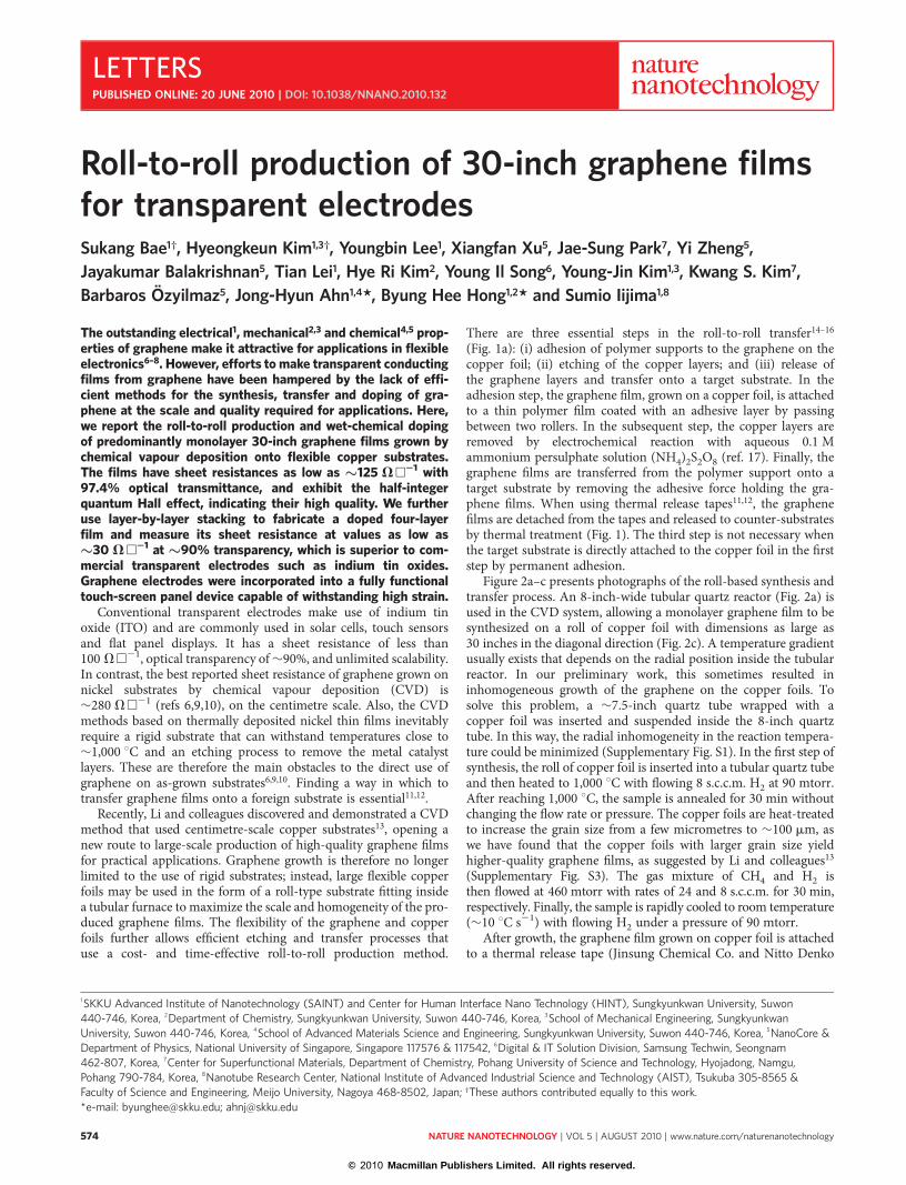
There are three essential steps in the roll-to-roll transfer14–16
(Fig. 1a): (i) adhesion of polymer supports to the graphene on thecopper foil; (ii) etching of the copper layers; and (iii) release ofthe graphene layers and transfer onto a target substrate. In theadhesion step, the graphene film, grown on a copper foil, is attachedto a thin polymer film coated with an adhesive layer by passingbetween two rollers. In the subsequent step, the copper layers areremoved by electrochemical reaction with aqueous 0.1 Mammonium persulphate solution (NH4)2S2O8 (ref. 17). Finally, thegraphene films are transferred from the polymer support onto atarget substrate by removing the adhesive force holding the gra-phene films. When using thermal release tapes11,12, the graphenefilms are detached from the tapes and released to counter-substratesby thermal treatment (Fig. 1). The third step is not necessary whenthe target substrate is directly attached to the copper foil in the firststep by permanent adhesion.
Figure 2a–c presents photographs of the roll-based synthesis andtransfer process. An 8-inch-wide tubular quartz reactor (Fig. 2a) isused in the CVD system, allowing a monolayer graphene film to besynthesized on a roll of copper foil with dimensions as large as30 inches in the diagonal direction (Fig. 2c). A temperature gradientusually exists that depends on the radial position inside the tubularreactor. In our preliminary work, this sometimes resulted ininhomogeneous growth of the graphene on the copper foils. Tosolve this problem, a �7.5-inch quartz tube wrapped with acopper foil was inserted and suspended inside the 8-inch quartztube. In this way, the radial inhomogeneity in the reaction tempera-ture could be minimized (Supplementary Fig. S1). In the first step ofsynthesis, the roll of copper foil is inserted into a tubular quartz tubeand then heated to 1,000 8C with flowing 8 s.c.c.m. H2 at 90 mtorr.After reaching 1,000 8C, the sample is annealed for 30 min withoutchanging the flow rate or pressure. The copper foils are heat-treatedto increase the grain size from a few micrometres to �100 mm, aswe have found that the copper foils with larger grain size yieldhigher-quality graphene films, as suggested by Li and colleagues13
(Supplementary Fig. S3). The gas mixture of CH4 and H2 isthen flowed at 460 mtorr with rates of 24 and 8 s.c.c.m. for 30 min,respectively. Finally, the sample is rapidly cooled to room temperature(�10 8C s21) with flowing H2 under a pressure of 90 mtorr.
After growth, the graphene film grown on copper foil is attachedto a thermal release tape (Jinsung Chemical Co. and Nitto Denko
1SKKU Advanced Institute of Nanotechnology (SAINT) and Center for Human Interface Nano Technology (HINT), Sungkyunkwan University, Suwon440-746, Korea, 2Department of Chemistry, Sungkyunkwan University, Suwon 440-746, Korea, 3School of Mechanical Engineering, SungkyunkwanUniversity, Suwon 440-746, Korea, 4School of Advanced Materials Science and Engineering, Sungkyunkwan University, Suwon 440-746, Korea, 5NanoCore &Department of Physics, National University of Singapore, Singapore 117576 & 117542, 6Digital & IT Solution Division, Samsung Techwin, Seongnam462-807, Korea, 7Center for Superfunctional Materials, Department of Chemistry, Pohang University of Science and Technology, Hyojadong, Namgu,Pohang 790-784, Korea, 8Nanotube Research Center, National Institute of Advanced Industrial Science and Technology (AIST), Tsukuba 305-8565 &Faculty of Science and Engineering, Meijo University, Nagoya 468-8502, Japan; †These authors contributed equally to this work.
*e-mail: [email protected]; [email protected]
LETTERSPUBLISHED ONLINE: 20 JUNE 2010 | DOI: 10.1038/NNANO.2010.132
NATURE NANOTECHNOLOGY | VOL 5 | AUGUST 2010 | www.nature.com/naturenanotechnology574
© 2010 Macmillan Publishers Limited. All rights reserved.
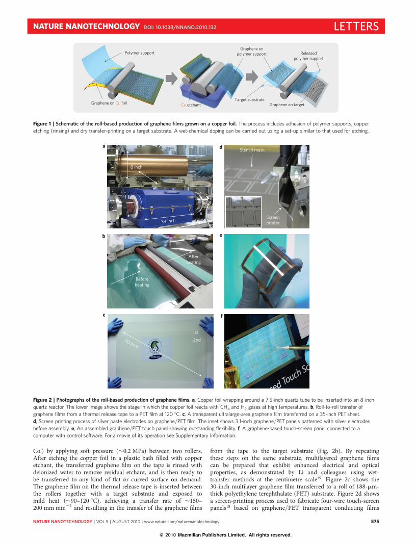
Co.) by applying soft pressure (�0.2 MPa) between two rollers.After etching the copper foil in a plastic bath filled with copperetchant, the transferred graphene film on the tape is rinsed withdeionized water to remove residual etchant, and is then ready tobe transferred to any kind of flat or curved surface on demand.The graphene film on the thermal release tape is inserted betweenthe rollers together with a target substrate and exposed tomild heat (�90–120 8C), achieving a transfer rate of �150–200 mm min21 and resulting in the transfer of the graphene films
from the tape to the target substrate (Fig. 2b). By repeatingthese steps on the same substrate, multilayered graphene filmscan be prepared that exhibit enhanced electrical and opticalproperties, as demonstrated by Li and colleagues using wet-transfer methods at the centimetre scale19. Figure 2c shows the30-inch multilayer graphene film transferred to a roll of 188-mm-thick polyethylene terephthalate (PET) substrate. Figure 2d showsa screen-printing process used to fabricate four-wire touch-screenpanels18 based on graphene/PET transparent conducting films
1st2nd30 inch
Beforeheating
Afterheating
39 inch
8 inch
Stencil mask
Screenprinter
a d
b e
c f
Figure 2 | Photographs of the roll-based production of graphene films. a, Copper foil wrapping around a 7.5-inch quartz tube to be inserted into an 8-inch
quartz reactor. The lower image shows the stage in which the copper foil reacts with CH4 and H2 gases at high temperatures. b, Roll-to-roll transfer of
graphene films from a thermal release tape to a PET film at 120 8C. c, A transparent ultralarge-area graphene film transferred on a 35-inch PET sheet.
d, Screen printing process of silver paste electrodes on graphene/PET film. The inset shows 3.1-inch graphene/PET panels patterned with silver electrodes
before assembly. e, An assembled graphene/PET touch panel showing outstanding flexibility. f, A graphene-based touch-screen panel connected to a
computer with control software. For a movie of its operation see Supplementary Information.
Graphene on Cu foil
Polymer support
Cu etchant
Graphene onpolymer support
Target substrateGraphene on target
Releasedpolymer support
Figure 1 | Schematic of the roll-based production of graphene films grown on a copper foil. The process includes adhesion of polymer supports, copper
etching (rinsing) and dry transfer-printing on a target substrate. A wet-chemical doping can be carried out using a set-up similar to that used for etching.
NATURE NANOTECHNOLOGY DOI: 10.1038/NNANO.2010.132 LETTERS
NATURE NANOTECHNOLOGY | VOL 5 | AUGUST 2010 | www.nature.com/naturenanotechnology 575
© 2010 Macmillan Publishers Limited. All rights reserved.
(Supplementary Fig. S12). After printing electrodes and dotspacers, the upper and lower panels are carefully assembledand connected to a controller installed in a laptop computer(Fig. 2e–f ), which shows extraordinary flexibility as we willdiscuss later (Fig. 4d). The scalability and processability of CVDgraphene and the roll-to-roll methods presented here are expectedto enable the continuous production of graphene-based electronicdevices at large scales.
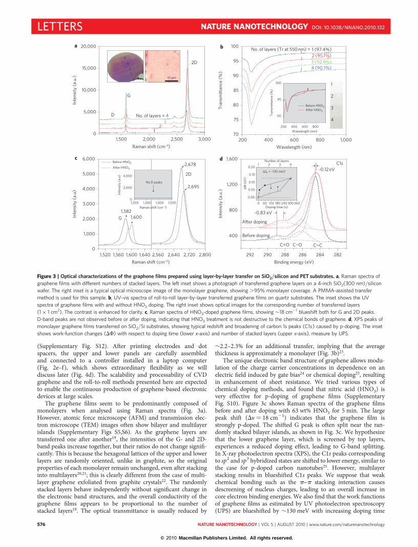
The graphene films seem to be predominantly composed ofmonolayers when analysed using Raman spectra (Fig. 3a).However, atomic force microscope (AFM) and transmission elec-tron microscope (TEM) images often show bilayer and multilayerislands (Supplementary Figs S5,S6). As the graphene layers aretransferred one after another19, the intensities of the G- and 2D-band peaks increase together, but their ratios do not change signifi-cantly. This is because the hexagonal lattices of the upper and lowerlayers are randomly oriented, unlike in graphite, so the originalproperties of each monolayer remain unchanged, even after stackinginto multilayers20,21; this is clearly different from the case of multi-layer graphene exfoliated from graphite crystals22. The randomlystacked layers behave independently without significant change inthe electronic band structures, and the overall conductivity of thegraphene films appears to be proportional to the number ofstacked layers19. The optical transmittance is usually reduced by
�2.2–2.3% for an additional transfer, implying that the averagethickness is approximately a monolayer (Fig. 3b)23.
The unique electronic band structure of graphene allows modu-lation of the charge carrier concentrations in dependence on anelectric field induced by gate bias24 or chemical doping25, resultingin enhancement of sheet resistance. We tried various types ofchemical doping methods, and found that nitric acid (HNO3) isvery effective for p-doping of graphene films (SupplementaryFig. S10). Figure 3c shows Raman spectra of the graphene filmsbefore and after doping with 63 wt% HNO3 for 5 min. The largepeak shift (Dn¼ 18 cm21) indicates that the graphene film isstrongly p-doped. The shifted G peak is often split near the ran-domly stacked bilayer islands, as shown in Fig. 3c. We hypothesizethat the lower graphene layer, which is screened by top layers,experiences a reduced doping effect, leading to G-band splitting.In X-ray photoelectron spectra (XPS), the C1s peaks correspondingto sp2 and sp3 hybridized states are shifted to lower energy, similar tothe case for p-doped carbon nanotubes25. However, multilayerstacking results in blueshifted C1s peaks. We suppose that weakchemical bonding such as the p–p stacking interaction causesdescreening of nucleus charges, leading to an overall increase incore electron binding energies. We also find that the work functionsof graphene films as estimated by UV photoelectron spectroscopy(UPS) are blueshifted by �130 meV with increasing doping time
1,500 2,000 2,500 3,0000
5,000
10,000
15,000
20,000
Inte
nsity
(a.u
.)
Raman shift (cm−1)
a
21
34
200 400 600 800 1,00070
75
80
85
90
95
100
Tran
smitt
ance
(%)
Wavelength (nm)
2 (95.1%)1 (97.4%)
3 (92.9%)4 (90.1%)
No. of layers (Tr at 550 nm) =
12
3
4
0 10 μm0
1
2
3
2,560 2,640 2,720 2,800
2,695
2,678
1,520 1,560 1,600 1,6400
1,000
2,000
3,000
4,000
5,000
6,000
1,6001,582
Inte
nsity
(a.u
)
Raman shift (cm−1)
c
1,200 1,300 1,400 1,5000
2,000
4,000
Inte
nsity
(a.u
)
Raman shift (cm−1)
No D peaks
D
G
2D
2D
G
200 400 600 800
90
95
100
Tran
smitt
ance
(%)
Wavelength (nm)
Before HNO3After HNO3
Before HNO3
After HNO3
0 60 120 180 240 300 360
0.00
0.05
0.10
0.15
0.201 2 3 4
Number of layers
Doping time (s)
b
d
1
2
3
4
292 290 288 286 284 282
400
800
1,200
1,600
After doping
Before doping
C1s
~0.83 eV
~0.12 eV
Inte
nsity
(a.u
.)
Binding energy (eV)
C=O C−O C−C
No. of layers =
ΔΦ (e
V)
ΔEF = ~130 meV
Figure 3 | Optical characterizations of the graphene films prepared using layer-by-layer transfer on SiO2/silicon and PET substrates. a, Raman spectra of
graphene films with different numbers of stacked layers. The left inset shows a photograph of transferred graphene layers on a 4-inch SiO2(300 nm)/silicon
wafer. The right inset is a typical optical microscope image of the monolayer graphene, showing .95% monolayer coverage. A PMMA-assisted transfer
method is used for this sample. b, UV–vis spectra of roll-to-roll layer-by-layer transferred graphene films on quartz substrates. The inset shows the UV
spectra of graphene films with and without HNO3 doping. The right inset shows optical images for the corresponding number of transferred layers
(1 × 1 cm2). The contrast is enhanced for clarity. c, Raman spectra of HNO3-doped graphene films, showing �18 cm21 blueshift both for G and 2D peaks.
D-band peaks are not observed before or after doping, indicating that HNO3 treatment is not destructive to the chemical bonds of graphene. d, XPS peaks of
monolayer graphene films transferred on SiO2/Si substrates, showing typical redshift and broadening of carbon 1s peaks (C1s) caused by p-doping. The inset
shows work-function changes (DF) with respect to doping time (lower x-axis) and number of stacked layers (upper x-axis), measure by UPS.
LETTERS NATURE NANOTECHNOLOGY DOI: 10.1038/NNANO.2010.132
NATURE NANOTECHNOLOGY | VOL 5 | AUGUST 2010 | www.nature.com/naturenanotechnology576
© 2010 Macmillan Publishers Limited. All rights reserved.
(Fig. 3d, inset). The multiple stacking also changes the work func-tions (Fig. 3d, inset; see also Supplementary Fig. S7 and Table S1),which could be very important in controlling the efficiency ofphotovoltaic26 or light-emitting devices based on graphene trans-parent electrodes27.
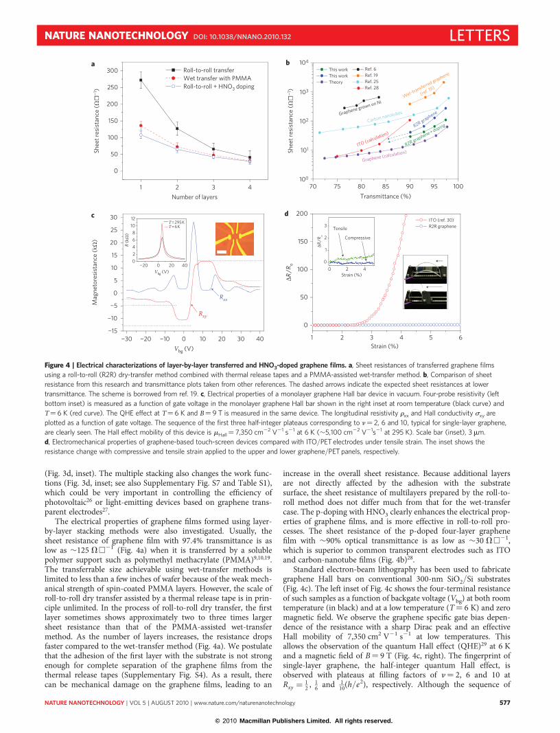
The electrical properties of graphene films formed using layer-by-layer stacking methods were also investigated. Usually, thesheet resistance of graphene film with 97.4% transmittance is aslow as �125 VA21 (Fig. 4a) when it is transferred by a solublepolymer support such as polymethyl methacrylate (PMMA)9,10,19.The transferrable size achievable using wet-transfer methods islimited to less than a few inches of wafer because of the weak mech-anical strength of spin-coated PMMA layers. However, the scale ofroll-to-roll dry transfer assisted by a thermal release tape is in prin-ciple unlimited. In the process of roll-to-roll dry transfer, the firstlayer sometimes shows approximately two to three times largersheet resistance than that of the PMMA-assisted wet-transfermethod. As the number of layers increases, the resistance dropsfaster compared to the wet-transfer method (Fig. 4a). We postulatethat the adhesion of the first layer with the substrate is not strongenough for complete separation of the graphene films from thethermal release tapes (Supplementary Fig. S4). As a result, therecan be mechanical damage on the graphene films, leading to an
increase in the overall sheet resistance. Because additional layersare not directly affected by the adhesion with the substratesurface, the sheet resistance of multilayers prepared by the roll-to-roll method does not differ much from that for the wet-transfercase. The p-doping with HNO3 clearly enhances the electrical prop-erties of graphene films, and is more effective in roll-to-roll pro-cesses. The sheet resistance of the p-doped four-layer graphenefilm with �90% optical transmittance is as low as �30 VA21,which is superior to common transparent electrodes such as ITOand carbon-nanotube films (Fig. 4b)28.
Standard electron-beam lithography has been used to fabricategraphene Hall bars on conventional 300-nm SiO2/Si substrates(Fig. 4c). The left inset of Fig. 4c shows the four-terminal resistanceof such samples as a function of backgate voltage (Vbg) at both roomtemperature (in black) and at a low temperature (T¼ 6 K) and zeromagnetic field. We observe the graphene specific gate bias depen-dence of the resistance with a sharp Dirac peak and an effectiveHall mobility of 7,350 cm2 V21 s21 at low temperatures. Thisallows the observation of the quantum Hall effect (QHE)29 at 6 Kand a magnetic field of B¼ 9 T (Fig. 4c, right). The fingerprint ofsingle-layer graphene, the half-integer quantum Hall effect, isobserved with plateaus at filling factors of n¼ 2, 6 and 10 atRxy = 1
2 , 16 and 1
10(h/e2), respectively. Although the sequence of
b
Tensile
Compressive
70 75 80 85 90 95 100100
101
102
103
104
Graphene (calculation)
This work Ref. 6This work Ref. 19Theory Ref. 25
Ref. 28
R2R graphene + doping
Graphene grown on Ni
R2R graphene
Wet-transferred graphene
(ref. 19)
ITO (calculation)
Carbon nanotubes
Transmittance (%)1 2 3 4
0
50
100
150
200
250
300
Shee
t res
ista
nce
(Ω☐
−1)
Shee
t res
ista
nce
(Ω☐
−1)
Number of layers
Roll-to-roll transferWet transfer with PMMARoll-to-roll + HNO3 doping
1 2 3 4 5 6
0
50
100
150
200ITO (ref. 30)R2R graphene
ΔR/R
o
ΔR/R
o
Strain (%)−30 −20 −10 0 10 20 30 40
−15
−10
−5
0
5
10
15
20
25
30
−20 0 20 4002468
1012
T = 295 KT = 6 K
R (k
Ω)
Vbg (V)
Vbg (V)
Mag
neto
resi
stan
ce (k
Ω)
Rxx
Rxy
c
a
d
0
1
2
2
3
40Strain (%)
Figure 4 | Electrical characterizations of layer-by-layer transferred and HNO3-doped graphene films. a, Sheet resistances of transferred graphene films
using a roll-to-roll (R2R) dry-transfer method combined with thermal release tapes and a PMMA-assisted wet-transfer method. b, Comparison of sheet
resistance from this research and transmittance plots taken from other references. The dashed arrows indicate the expected sheet resistances at lower
transmittance. The scheme is borrowed from ref. 19. c, Electrical properties of a monolayer graphene Hall bar device in vacuum. Four-probe resistivity (left
bottom inset) is measured as a function of gate voltage in the monolayer graphene Hall bar shown in the right inset at room temperature (black curve) and
T¼ 6 K (red curve). The QHE effect at T¼ 6 K and B¼ 9 T is measured in the same device. The longitudinal resistivity rxx and Hall conductivity sxy are
plotted as a function of gate voltage. The sequence of the first three half-integer plateaus corresponding to n¼ 2, 6 and 10, typical for single-layer graphene,
are clearly seen. The Hall effect mobility of this device is mHall¼ 7,350 cm22 V21 s21 at 6 K (�5,100 cm22 V21s21 at 295 K). Scale bar (inset), 3 mm.
d, Electromechanical properties of graphene-based touch-screen devices compared with ITO/PET electrodes under tensile strain. The inset shows the
resistance change with compressive and tensile strain applied to the upper and lower graphene/PET panels, respectively.
NATURE NANOTECHNOLOGY DOI: 10.1038/NNANO.2010.132 LETTERS
NATURE NANOTECHNOLOGY | VOL 5 | AUGUST 2010 | www.nature.com/naturenanotechnology 577
© 2010 Macmillan Publishers Limited. All rights reserved.
the plateaus remains for both the electron side and the hole side,there is a slight deviation from the fully quantized values on thehole side.
Finally, the electromechanical properties of graphene/PETtouch-screen panels were tested (Fig. 4d; Supplementary Fig. S2).Unlike an ITO-based touch panel, which easily breaks under�2–3% strain, the graphene-based panel resists up to 6% strain;this is limited not by the graphene itself, but by the printed silverelectrodes (Fig. 4d)30.
In summary, we have developed and demonstrated the roll-to-roll production of graphene on ultralarge copper substrates.The multiple transfer and simple chemical doping of graphenefilms considerably enhances its electrical and opticalproperties. Given the scalability and processability of roll-to-rolland CVD methods and the flexibility and conductivity of graphenefilms, we anticipate that the commercial production of large-scaletransparent electrodes, replacing ITO, will be realized in thenear future.
Received 11 March 2010; accepted 28 May 2010;published online 20 June 2010; corrected online 25 June 2010
References1. Geim, A. K. & Novoselov, K. S. The rise of graphene. Nature Mater. 6,
183–191 (2007).2. Lee, C., Wei, X., Kysar, J. W. & Hone, J. Measurement of the elastic properties
and intrinsic strength of monolayer graphene. Science 321, 385–388 (2008).3. Bunch, J. S. et al. Impermeable atomic membranes from graphene sheets. Nano
Lett. 8, 2458–2462 (2008).4. Elias, D. C. et al. Control of graphene’s properties by reversible hydrogenation:
evidence for graphene. Science 323, 610–613 (2009).5. Wang, X. et al. N-doping of graphene through electrothermal reactions with
ammonia. Science 324, 768–771 (2009).6. Kim, K. S. et al. Large-scale pattern growth of graphene films for stretchable
transparent electrodes. Nature 457, 706–710 (2009).7. Kim, D.-H. et al. Stretchable and foldable silicon integrated circuits. Science 320,
507–511 (2008).8. Sekitani, T. et al. A rubberlike stretchable active matrix using elastic conductors.
Science 321, 1468–1472 (2008).9. Reina, A. et al. Large area, few-layer graphene films on arbitrary substrates by
chemical vapor deposition. Nano Lett. 9, 30–35 (2009).10. Cai, W. W. et al. Large area few-layer graphene/graphite films as transparent
thin conducting electrodes. Appl. Phys. Lett. 95, 123115 (2009).11. Lee, Y. et al. Wafer-scale synthesis and transfer of graphene films. Nano Lett. 10,
490–493 (2010).12. Caldwell, J. D. et al. Technique for the dry transfer of epitaxial graphene onto
arbitrary substrates. ACS Nano 4, 1108–1114 (2010).13. Li, X. et al. Large-area synthesis of high-quality and uniform graphene films on
copper foils. Science 324, 1312–1314 (2009).14. Ahn, S. H. & Guo, L. J. High-speed roll-to-roll nanoimprint lithography on
flexible plastic substrates. Adv. Mater. 20, 2044–2049 (2008).15. Yerushalmi, R., Jacobson, Z. A., Ho, J. C., Fan, Z. & Javey, A. Large scale, highly
ordered assembly of nanowire parallel arrays by differential roll printing. Appl.Phys. Lett. 91, 203104 (2007).
16. Chang, Y. K. & Hong, F. C. The fabrication of ZnO nanowire field-effecttransistors by roll-transfer printing. Nanotechnology 20, 195302 (2009).
17. Jo, G. et al. Etching solution for etching Cu and Cu/Ti metal layer of liquidcrystal display device and method of fabricating the same. US patent,6,881,679 (2005).
18. Hecht, D. S. et al. Carbon nanotube film on plastic as transparent electrode forresistive touch screens. J. Soc. Inf. Display 17, 941–946 (2009).
19. Li, X. et al. Transfer of large-area graphene films for high-performancetransparent conductive electrodes. Nano Lett. 9, 4359–4363 (2009).
20. Hass, J. et al. Why multilayer graphene on 4H-SiC(000–1) behaves like a singlesheet of graphene. Phys. Rev. Lett. 100, 125504 (2008).
21. Sprinkle, M. et al. First direct observation of a nearly ideal graphene bandstructure. Phys. Rev. Lett. 103, 226803 (2009).
22. Ferrari, A. C. et al. Raman spectrum of graphene and graphene layers. Phys. Rev.Lett. 97, 187401 (2006).
23. Nair, R. R. et al. Fine structure constant defines visual transparency of graphene.Science 320, 1308 (2008).
24. Das, A. et al. Monitoring dopants by Raman scattering in an electrochemicallytop-gated graphene transistor. Nature Nanotech. 3, 210–215 (2008).
25. Geng, H.-Z. et al. Effect of acid treatment on carbon nanotube-based flexibletransparent conducting films. J. Am. Chem. Soc. 129, 7758–7759 (2007).
26. Schrivera, M., Reganb, W., Losterb, M. & Zettl, A. Carbon nanostructure–aSi:Hphotovoltaic cells with high open-circuit voltage fabricated without dopants.Solid State Commun. 150, 561–563 (2010).
27. Wu, J. et al. Organic light-emitting diodes on solution-processed graphenetransparent electrodes. ACS Nano 4, 43–48 (2010).
28. Lee, J.-Y., Connor, S. T., Cui, Y. & Peumans, P. Solution-processed metalnanowire mesh transparent electrodes. Nano Lett. 8, 689–692 (2008).
29. Cao, H. L. et al. Electronic transport in chemical vapor deposited graphenesynthesized on Cu: Quantum Hall effect and weak localization. Appl. Phys. Lett.96, 122106 (2010).
30. Cairns, D. R. et al. Strain-dependent electrical resistance of tin-doped indiumoxide on polymer substrates. Appl. Phys. Lett. 76, 1425–1427 (2000).
AcknowledgementsThis work was supported by the National Research Foundation of Korea (NRF), fundedby the Ministry of Education, Science and Technology (2009-0081966, 2009-0082608,2009-0083540, 2009-0090017, World Class University R33-2008-000-10138-0, NationalHonor Scientist Program), the Research Centre of Breakthrough Technology Programthrough the Korea Institute of Energy Technology Evaluation and Planning (KETEP),funded by the Ministry of Knowledge Economy (2009-3021010030-11-1), SingaporeNational Research Foundation (NRF-RF2008-07) & NUS NanoCore, and T.J. Park JuniorFaculty Fellowship. The authors thank R. Ruoff (University of Texas at Austin) and P. Kim(Columbia University) for helpful comments, W.S. Lim, K.D. Kim and Y.D. Kim (SKKU)for assistance in XPS analysis, and Samkwang Well Tech Co. for assistance with the touch-panel fabrication.
Author contributionsB.H.H. planned and supervised the project, with assistance in supervision from J.H.A.Y.-J.K., B.O., K.S.K. and S.I. provided advice for the project. B.H.H., S.B. and H.K. conceivedand carried out the experiment. B.H.H., J.H.A. and B.O. analysed the data and wrote themanuscript. X.X., J.B., Y.Z. and B.O. fabricated the QHE devices, and carried out themeasurements. Y.L. and Y.I.S. helped with the fabrication of touch-screen panels andelectromechanical analysis. J.S.P., H.R.K. and T.L. helped with the doping experiment.
Additional informationThe authors declare no competing financial interests. Supplementary informationaccompanies this paper at www.nature.com/naturenanotechnology. Reprints andpermission information is available online at http://npg.nature.com/reprintsandpermissions/.Correspondence and requests for materials should be addressed to B.H.H. and J.H.A.
LETTERS NATURE NANOTECHNOLOGY DOI: 10.1038/NNANO.2010.132
NATURE NANOTECHNOLOGY | VOL 5 | AUGUST 2010 | www.nature.com/naturenanotechnology578
© 2010 Macmillan Publishers Limited. All rights reserved.