s c workshop 2 cryo-em training for beginners …...dqe and binning anti-aliased bin=0.9 hardware...
TRANSCRIPT

S2C2 Workshop – Cryo-EM Training for Beginners
Christopher Booth
Gatan Inc.
Jan 22, 2019

Key Concepts in Detecting Electrons

Key Concepts in Detecting Electrons
• CMOS and CCD
• “indirect” vs direct detection cameras
• Sensitivity
• Linearity and dynamic range
• Dynamic range
• Pixel size and field of view
• Electron counting
• Co-incidence loss

Recording Images In Electron MicroscopyA little bit of history
• Oldest recording medium: photographic film
• 1970: Charge coupled device (CCD) was invented
• 1976: CCD camera was used for astronomy
• 1982: 100 x 100 CCD was directly exposed to 100 kV
electrons…radiation damage
• 1988: 576 x 382 CCD used with scintillator and optical
coupler
• 1990: Gatan made the world’s first commercial CCD
camera
• 2002: 128 x 128 direct detection camera developed
• 2008 – 2009: commercial complementary metal-oxide
semiconductor (CMOS) cameras and radiation hard
CMOS cameras were introduced

CCD vs. CMOS
Both CCD and CMOS use photo diodes to convert photons to electrons,
the difference is how they store charge and transfer it.
• CCD: Charge is transferred between neighboring cells, and read-out
• CMOS : Charge immediately converted to voltage (read out with digital output)
http://meroli.web.cern.ch/meroli/lecture_cmos_vs_ccd_pixel_sensor.html

Detectors in Electron Microscopy
A. Optically coupled
B. Fiber-optic coupling
C. Direct detection
D. Transmission direct detection

Traditional Indirect Detection
e-
Scintillator
Light transfer
Light sensitive CCD or CMOS
1. Convert
electrons to
light
2. Transfer light to
detector
3. Detect light and
convert to
signal

Direct Detection
e-
Radiation hard CMOS
1. Convert
electrons to
light
2. Transfer light to
detector
3. Detect electron
and convert to
signal

Transmission Direct Detection
e-
Radiation hard, thinned CMOS
1. Convert
electrons to
light
2. Transfer light to
detector
3. Detect electron
and convert to
signal Minimize back
scattered
electrons that
add noise

Sensitivity
• Minimum detectable signal in terms of the number of incident electrons.
• Single-electron sensitivity
• if the gain of the system is such that the output of a single incident electron is above the
noise floor
electrons or counts
freq
uen
cy
Noise floorSignal from incident electrons

Linearity
• Relationship between output (image
intensity in digital units) and the input
(number of incident electrons).
• CMOS and CCDS are much more linear
than film
• Counted cameras have a special kind of
non-linearity called co-incidence loss
Journal of Microscopy, Vol. 200, Pt 1, 2000, pp. 1±13.

Dynamic Range
Dynamic range: The range of values that can be distinguished between a maximum level
(saturation) and zero (noise)
• Driven by combination of max allowable charge in each and noise floor
• One pixel can have 16 bit dynamic range (values between 0 – 16000)
• Used to be a very important factor for cameras, now frame rate is much more important
• A camera with only 12 bit dynamic range (0 – 4095) might accumulate 40 frames in a
second.
• 4095 x 20 = 163,800 counts of dynamic range
Journal of Microscopy, Vol. 200, Pt 1, 2000, pp. 1±13.

3,71
0 pi
xels
3,838 pixelsK2
,4.0
92 p
ixel
s
5,760 pixelsK3
23.6 Mpixels(94 Mpixels super-resolution)
14.4 Mpixels
How Many Pixels are Enough?

Rio™ 16: 4k x 4k, 9 µm
Rio 9: 3k x 3k, 9 µm
How Important is FOV?
OneView®: 4k x 4k, 15 µm
Rio 16: 4k x 4k, 9 µm
K3™ : 6k x 4k, 5 µm
K2®: 4k x 4k, 5 µm
Side-mount camera
Bottom-mount camera
CCD

Electron Counting Makes All the Difference
Single high speed frame using conventional
CCD-style charge read-out
Same frame after counting
Counting removes the variability from scattering,
rejects the electronic read-noise, and restores the DQE.

Traditional Integration
Similar to indirect detection cameras, direct detectors can integrate
the total charge produced when an electron strikes a pixel.
Electron enters
Detector.
Electron signal is
scattered.
Charge collects in
each pixel.

Counting
In counting mode, individual electron events are identified at the
time that they reach the detector. To do this efficiently the camera
must run fast enough so that individual electron events can be
identified separately.
Electron enters
Detector.
Electron signal is
scattered.
Charge collects in
each pixel.
Event reduced to
highest charge pixels.

Super-Resolution
The theoretical information limit defined by the physical pixel size is
surpassed when you use the K2 in super-resolution mode. The K2 sensor
pixel size is slightly smaller than the area that the electron interacts with;
as a result each incoming electron deposits signal in a small cluster of
pixels. High-speed electronics are able to recognize each electron event
(at 400 fps) and find the center of event with sub-pixel precision.
Electron enters
Detector.
Electron signal is
scattered.
Charge collects in
each pixel.
Event localized to
sub-pixel accuracy.

Electron Counting Requires that Electrons Don’t Overlap on
the Sensor
Faster frame
rate
Lower beam
intensity
Both methods
allow counting,
but the effect is
not equivalent!

Electron counting animation

0
20
40
60
80
100
120
0 20 40 60 80 100 120
Measure
d D
ose R
ate
(e
lectr
ons/p
ixel/second
Input Dose Rate (elctrons/pixel/second)
Perfect Detection: DQE of 1.0 with no
coincidence loss
K3 TF20: K3 coincidence loss curve
K2: Original coincidence loss curve
as measured at UCSF for Li et al
Nature Methods 2013 publication
Cameras working at 40 fps are very limited
in the range of conditions they can be used
“Counting camera” at 40 fps
K2
K3

Measuring Detector Performance

PSF, MTF, NTF and DQE?
• PSF: Point spread function
• Blurring of a single point in the camera
• MTF: Modulation transfer function
• PSF as a function of spatial frequency
• Most often estimated using a “knife
edge”
• NTF: Noise transfer function
• Noise power spectrum
• Noise as a function of spatial frequency
DQE s
=SNRout s
SNRin s
=MTF(s)2
ΤNPSout(s) Dosein(s)

DQE Challenges
• Signal challenges: Edge image non-ideality• Charging and edge cleanliness
• Scale
• Edge dose
• Motion
• Fields
• scatter
• Noise challenges: • Fixed pattern noise
• Calibration of noise power
• Measurement of incoming beam level
• Counting-related challenges: • spatial effects of coincidence loss: high-pass filtering
• Non-linear counting due to coincidence loss – calibration.
• background
𝐷𝑄𝐸 𝑠
=𝑆𝑁𝑅𝑜𝑢𝑡 𝑠
𝑆𝑁𝑅𝑖𝑛 𝑠
=Τ𝑆𝑃𝑆𝑜𝑢𝑡(𝑠) 𝑆𝑃𝑆𝑖𝑛(𝑠)
Τ𝑁𝑃𝑆𝑜𝑢𝑡(𝑠) 𝑁𝑃𝑆𝑖𝑛(𝑠)
=𝑀𝑇𝐹(𝑠)2
Τ𝑁𝑃𝑆𝑜𝑢𝑡(𝑠) 𝐷𝑜𝑠𝑒𝑖𝑛(𝑠)

Measuring MTF with a Physical Edge (1)
AuPd-coated and plasma cleaned edge with canted face mounted in the entrance aperture of a GIF Quantum®
imaged on the K2 at the end of the GIF in super-resolution mode at 200 kV. (particularly bad example – not
always this bad)
Effect of charging
Short traversal close to
surface charge
Long traversal
close to surface
charge
Canted
edge Wire
Scale at edge
At GIF
entrance
module
At pointer
K2 super-pixel
(2.5 µm)
UltraScan®
pixel
(15 µm)
400 nm 3 µm

Measuring MTF with a Physical Edge (2)
Motion – edge creep Noise
A noise-tolerant method for measuring MTF from
found-object edges in a TEM, Paul Mooney,
Microscopy and Microanalysis 15:1322-1323 CD
Cambridge University Press (2009). Figure 4:
Simulated MTF with various amounts of shot noise
added.
Motion – fields
Good: difference
between two 20 s
edge images
showing no “motion
fringe”.
At low dose rates, need long exposures to
get enough dose have to be careful
about edge creep.

Other Things to Avoid with DQE Measurements
• Missing dose in a Faraday cup holder: overestimates DCE and therefore DQE (in same proportion)
• Using the TEM screen calibration
• Drifting beam current
• Over- or under- values MTF(0) or DCE
• Leaving specimen holder inserted during MTF measurement Charging of specimen and/or holder can move image of edge shadow.

DQE and Binning
0
0.1
0.2
0.3
0.4
0.5
0.6
0.7
0.8
0.9
1
0 0.1 0.2 0.3 0.4 0.5 0.6 0.7 0.8 0.9 1

DQE and Binning
0
0.1
0.2
0.3
0.4
0.5
0.6
0.7
0.8
0.9
1
0 0.1 0.2 0.3 0.4 0.5 0.6 0.7 0.8 0.9 1
hardware bin=2
hardware bin=1
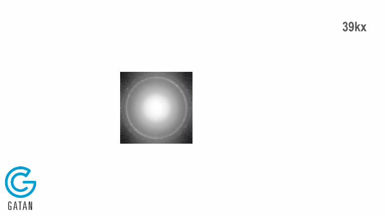
A visual representation of Aliasing: 39kx

31kx

23kx

An FFT is calculated
as though each
image were bordered
by an infinite number
of neighbors
39kx

As you drop the
magnification, the
information from one
region begins to
show up in the
neighboring region
31kx

It becomes very
obvious with a strong
signal at low
magnification
23kx
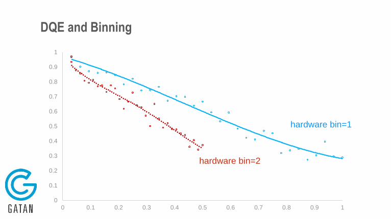
DQE and Binning
0
0.1
0.2
0.3
0.4
0.5
0.6
0.7
0.8
0.9
1
0 0.1 0.2 0.3 0.4 0.5 0.6 0.7 0.8 0.9 1
hardware bin=2
hardware bin=1

DQE and Binning
0
0.1
0.2
0.3
0.4
0.5
0.6
0.7
0.8
0.9
1
0 0.1 0.2 0.3 0.4 0.5 0.6 0.7 0.8 0.9 1
hardware bin=2
Anti-aliased bin=2

DQE and Binning
0
0.1
0.2
0.3
0.4
0.5
0.6
0.7
0.8
0.9
1
0 0.1 0.2 0.3 0.4 0.5 0.6 0.7 0.8 0.9 1
hardware bin=2
Anti-aliased bin=1.5

0
0.1
0.2
0.3
0.4
0.5
0.6
0.7
0.8
0.9
1
0 0.1 0.2 0.3 0.4 0.5 0.6 0.7 0.8 0.9 1 1.1
DQE and Binning
Anti-aliased bin=0.9
hardware bin=2

Measuring Image Performance Using Thon Rings
Thon rings are a indicator of
performance.
However, they are a system
test and really hard to
compare quantitatively.

Practical Considerations in Data Collection

Dark Subtraction
• Removes the noise
baseline from the image
• New dark references are
often taken once a day
Dark image

Gain Correction
• Gain correction normalizes the response of each pixel to an electron
• This is why images are often floating point values
• In K3 we are allowing integer gain normalization
• Each electron is 32 counts
• Usually collected once per week
Gain map

Defect Correction
• Removes poorly performing pixels
• Hot
• Dark
• Unstable
• Defect pixels contribute to fixed pattern noise
• Usually updated with Gain Reference
Defect map(enlarged detail)

Defect map
(enlarged detail)
Uncorrected image
Corrected image
Dark image
Gain map
-
Typical Gain Correction Scheme

Counted Gain Correction Scheme
-
Linear Image Correction Counted Image Correction
Electron
CountingRaw
Linear
Dark
Linear
Gain
Linear
Defect
LinearUn-proc
Counted
Counted
Gain Ref
Counted
Defect
Final
Counted
Electron
Counting

Image: Uniform intensity FFT: White noise
Checking the Quality of Image Correction

Measurement of Fixed Pattern Noise (FPN)
Uniform A
Uniform B
Center of Xcorr
FPN = 0.0106
Uniform A Uniform B⊗
Uniform illumination
Common defects, dark image and gain image
Frame rate = 75 fr/s, (0.0133156 s/fr), all images.
Total dose = 14 e/pix, all images
FPN = peak pixel valueCross-correlation map

E
#
Readout noise Complete absorption of electron by detector (only for low E electrons or very large pixels)
Traversing electrons
False negativesFalse positives
Improved Noise Also Allows us to Improve Electron Countability

Dose rate on the detector
Mean number of electrons hitting
a detector pixel per unit time.
Total dose at the sample
Number of electrons that traverse a
unit area of the sample during the
exposure of this image frame.

At 8-bit/pixel, gain-corrected data saturates with a value of 255.
The saturation monitor reports the percentage of pixels that have reached saturation in a single frame.
Keeping track of Pixel Saturation in K3

How Frame Alignment Works
Raw counted frame Final aligned image

+ + ... +
* ... **
=
=
Raw counted frames are summed
Sub-frames are aligned and summed
1 sub-frame
1 final image

Sensor
Frame
Rate Dose Rate Counted Frame Sub-frame
Summed/Aligned
Frame
Other 40 0.8 e/pix/s 0.025 s 1 s (1 fps) 100 s
K2 400 8 e/pix/s 0.0025 s 0.1 s (10 fps) 10 s
K3 1500 30 e/pix/s 0.00066 s 0.027 s (37 fps) 2.7 s
No motion
correctionMotion
correction

MotionCor2 -InMrc Stack.mrc -OutMrc CorrectedSum.mrc -Patch 5 5 -FtBin 1.2 -Iter 10 -FmDose 1.2 -bft 1.1 -Tol 0.5
MotionCor2 on the K3

Annealing Prevents Contamination Buildup
Without
annealing
• A cold sensor is essentially a vacuum pump. Contamination builds up on its cold surface and, if left unchecked over prolonged
times, will accumulate to the point of degrade data quality
• Severe contamination may even become evident on the gain reference images, as in the example below of a K2 sensor
After
annealing

• Regular annealing of the sensor
reduces background levels and
surface contamination
• It can also help to repair some
radiation damage
• If the camera is used for a
prolonged time without warming,
the electron beam can harden any
contaminants, making the CMOS
detector difficult to clean
• Annealing should be done at the
end of every session one day long
or longer
• Every time you do a cryo-cycle is a
good idea
Camera Heating/Annealing

Future Directions for Electron Detection

Throughput is Going to be Critical
• We should be aiming to collect enough data in a few hours
• K3 + Latitude + Titan Krios

Improving Throughput: Larger Sensors
• One chance to expose a specimen area
• If the pixel quality is high, larger sensors
reduce the number of images needed
K3
K2

Improving Throughput: Faster Sensors
• Reduce exposure times during
counting
• Exposure times: 100 s to 10 s to 1 s
• Reduce time for non-data images
during automation
• Focusing
• Centering

Improving Throughput
• Reducing exposure time and
increasing image size gives you
the biggest benefit
• K2: 6 images x 10 s = 60 s
• K3: 5 images x 2.5 s = 12.5 s
• K3: area is 25% larger

• Sample damage increases
during the exposure
• The first frames have the
least damage but the most
drift
Better Data Through Motion Correction

• Sample damage increases during the
exposure
• The first frames have the least
damage but the most drift
• Today the first 2 –3 frames are
excluded
• The K3 should be fast enough to let us
use frames 1 – 3 !
Better Data Through Motion Correction
