saeedian, meysam; pouresmaeil, edris; samadaei, emad ... · this is an electronic reprint of the...
TRANSCRIPT
This is an electronic reprint of the original article.This reprint may differ from the original in pagination and typographic detail.
Powered by TCPDF (www.tcpdf.org)
This material is protected by copyright and other intellectual property rights, and duplication or sale of all or part of any of the repository collections is not permitted, except that material may be duplicated by you for your research use or educational purposes in electronic or print form. You must obtain permission for any other use. Electronic or print copies may not be offered, whether for sale or otherwise to anyone who is not an authorised user.
Saeedian, Meysam; Pouresmaeil, Edris; Samadaei, Emad; Godinho Rodrigues, EduardoManuel; Godina, Radu; Marzband, MousaAn innovative dual-boost nine-level inverter with low-voltage rating switches
Published in:Energies
DOI:10.3390/en12020207
Published: 02/01/2019
Document VersionPublisher's PDF, also known as Version of record
Please cite the original version:Saeedian, M., Pouresmaeil, E., Samadaei, E., Godinho Rodrigues, E. M., Godina, R., & Marzband, M. (2019).An innovative dual-boost nine-level inverter with low-voltage rating switches. Energies, 12(2), [207].https://doi.org/10.3390/en12020207

energies
Article
An Innovative Dual-Boost Nine-Level Inverter withLow-Voltage Rating Switches
Meysam Saeedian 1 , Edris Pouresmaeil 1,* , Emad Samadaei 2 ,Eduardo Manuel Godinho Rodrigues 3, Radu Godina 4 and Mousa Marzband 5
1 Department of Electrical Engineering and Automation, Aalto University, 02150 Espoo, Finland;[email protected]
2 Department of Electronics Design (EKS), Mid Sweden University, Holmgatan 10, 85170 Sundsvall, Sweden;[email protected]
3 Management and Production Technologies of Northern Aveiro—ESAN, Estrada do Cercal 449, Santiago deRiba-Ul, 3720-509 Oliveira de Azeméis, Portugal; [email protected]
4 Research and Development Unit in Mechanical and Industrial Engineering (UNIDEMI), Department ofMechanical and Industrial Engineering, Faculty of Science and Technology (FCT), New University of Lisbon,2829-516 Caparica, Portugal; [email protected]
5 Department of Maths, Physics and Electrical Engineering, Faculty of Engineering and Environment,Northumbria University, Newcastle upon Tyne NE1 8ST, UK; [email protected]
* Correspondence: [email protected]; Tel.: +358-505-984-479
Received: 3 December 2018; Accepted: 4 January 2019; Published: 9 January 2019
Abstract: This article presents an innovative switched-capacitor based nine-level inverter employingsingle DC input for renewable and sustainable energy applications. The proposed configurationgenerates a step-up bipolar output voltage without end-side H-bridge, and the employed capacitorsare charged in a self-balancing form. Applying low-voltage rated switches is another merit of theproposed inverter, which leads to extensive reduction in total standing voltage. Thereby, switchinglosses as well as inverter cost are reduced proportionally. Furthermore, the comparative analysisagainst other state-of-the-art inverters depicts that the number of required power electronic devicesand implementation cost is reduced in the proposed structure. The working principle of the proposedcircuit along with its efficiency calculations and thermal modeling are elaborated in detail. In theend, simulations and experimental tests are conducted to validate the flawless performance of theproposed nine-level topology in power systems.
Keywords: power conversion; multilevel inverter; improved switched-capacitor module; multicarrier based modulation
1. Introduction
In recent years, extensive research has been carried out on multilevel inverters (MLIs) due to theirpotential in various industrial applications, particularly grid-connected renewable energy sources,machine drives, and high-voltage direct current transmission systems. Improved output waveformsquality, reduced device stress (dv/dt), and increased efficiency are some merits of the MLIs incomparison with the standard two-level inverter [1–4]. The most popular traditional/basic multileveltopologies are CHB, NPC, and FC, which have widely been put into commercial use in high/mediumvoltage systems (above 3 kV). Nonetheless, high control/modulation technique complexity andlarge power electronic device count (dc power supplies, semiconductors, and capacitors) are cited asdemerits of the aforementioned topologies [5–7].
To overcome these drawbacks, researchers and industrialists all around the world are contributingto present innovative topologies with the ability to produce more voltage levels with reduced device
Energies 2019, 12, 207; doi:10.3390/en12020207 www.mdpi.com/journal/energies

Energies 2019, 12, 207 2 of 15
count and to further improve energy efficiency. Apart from that, it has tried to develop MLIs withlower voltage-rating switches and to cope with the voltage unbalancing problem in NPC and FC. Theseattempts lead not only to reducing filter requirement and simplicity, but also cost/volume reduction ofthe conversion system [8–10].
Despite a plethora of multilevel topologies that have been presented, intensive effort has beendevoted to introduce promising topologies. For example, ref. [11,12] presented novel MLIs employingthe technique of switched-capacitor. Although a substantial reduction in the device count is achievedin these topologies as compared to the conventional ones, they however require H-bridge circuits togenerate bipolar voltages. This weakness leads to a sharp increase in total standing voltage (TSV)and thereupon switches cost. A single source nine-level (9 L) inverter has been proposed in [13],which applies semiconductors with the same Peak inverse voltage (PIV) equal to input voltage level.Nevertheless, this topology utilizes numerous insulated-gate bipolar transistors (IGBTs) and gatedrivers, which enlarge the system. A hybrid cascaded MLI with improved symmetrical sub-modulewas introduced in [14]. It employs four dc sources and ten switches with high PIVs to produce a 9 Lvoltage waveform. Furthermore, [15] introduced a single source inverter which is comprised of anH-bridge inverter and two switched-capacitor modules. It employs sixteen IGBTs with low voltageratings for generating a 7 L output voltage. Yet, these presented MLIs in the literature suffer fromeither a large number of circuit elements or relatively high PIVs.
In summary, the main contribution of this paper is the development of a modified 9 L inverterfor single phase systems, which is superior to all the earlier topologies. The switches employed inthe proposed configuration enjoy low PIVs. At the same time, a further reduction in device countand implementation cost is attained in the proposed circuit compared to the traditional/cutting-edgeones. Moreover, there is no difficulty in the capacitors’ charging process since the inverter is inherentlyself-balanced. Due to the voltage boosting capability, this inverter is proposed for grid-connectedrenewable energy sources (such as solar and wind farms), uninterruptible power supplies, andelectric vehicles in which low input DC voltages are required to be boosted to an acceptable range forthese systems.
The rest of this article is structured into five sections. Following the introduction, Section 2presents the operating principle and a detailed comparative study of the proposed topology in order todemonstrate the superiority of the proposed inverter against newest 9 L topologies. Section 3 describesPWM strategy applied to the proposed inverter. Efficiency calculations and thermal analysis are carriedout in Section 4. The simulation and experimental results are brought in Section 5 in order to provethe feasibility and effectiveness of the presented topology. Eventually, conclusions are presented inSection 6.
2. Analysis of the Proposed Nine-Level Inverter
2.1. Circuit Description
Figure 1 depicts the proposed switched-capacitor based inverter with the potential of generatinga 9 L staircase waveform (±2VIN, ±3VIN/2, ±VIN, ±VIN/2 and 0). As demonstrated in Figure 1,it comprises twelve power switches, two capacitors (C1, C2), and only one input DC source with theadvantage of regenerative capability. The output voltage can be boosted up to 2VIN by connecting theinput source with pre-charged capacitors in series. It should be underscored that the blocking voltageof all switches employed in the proposed inverter is equal to the input DC source (i.e., VIN), with theexception of S7, S8, and S12 which block only half the VIN. In other words, it generates a bipolar outputvoltage without using end-side H-bridge. This ability is considered a beneficial feature of the proposedcircuit since the lower switch voltage rating, the cheaper switch.
The working principle of the proposed inverter is illustrated in Figure 2. As can be observed,C1 and C2 are charged up to VIN/2 by turning S3 and S4 on during 0 and ±1VIN levels. Then, thecapacitors are connected in parallel at ±VIN/2 and ±3VIN/2 levels. Thereby, the voltage across them

Energies 2019, 12, 207 3 of 15
is balanced. Finally, they are discharged across the load during ±VIN/2 and ±2VIN levels. Relying onthis simple switching plan, the proposed inverter does not require any external balancer circuit.Energies 2019, 12, x FOR PEER REVIEW 3 of 15
VIN
S1
S2
S3 S5
S4 S6
S7
S8
S9
S10
S12
C1
C2
A BS11
VLoad=VA-VB+ -
R LILoad
Figure 1. The proposed 9 L topology.
The working principle of the proposed inverter is illustrated in Figure 2. As can be observed, C1 and C2 are charged up to VIN/2 by turning S3 and S4 on during 0 and ±1VIN levels. Then, the capacitors are connected in parallel at ±VIN/2 and ±3VIN/2 levels. Thereby, the voltage across them is balanced. Finally, they are discharged across the load during ±VIN/2 and ±2VIN levels. Relying on this simple switching plan, the proposed inverter does not require any external balancer circuit.
VIN
S1
S2
S3 S5
S4 S6
S7
S8
S9
S10
S12
C1
C2
A BS11
VIN
S1
S2
S3 S5
S4 S6
S7
S8
S9
S10
S12
C1
C2
A BS11
VIN
S1
S2
S3 S5
S4 S6
S7
S8
S9
S10
S12
C1
C2
A BS11
(a) (b) (c)
VIN
S1
S2
S3 S5
S4 S6
S7
S8
S9
S10
S12
C1
C2
A BS11
VIN
S1
S2
S3 S5
S4 S6
S7
S8
S9
S10
S12
C1
C2
A BS11
VIN
S1
S2
S3 S5
S4 S6
S7
S8
S9
S10
S12
C1
C2
A BS11
(d) (e) (f)
VIN
S1
S2
S3 S5
S4 S6
S7
S8
S9
S10
S12
C1
C2
A BS11
VIN
S1
S2
S3 S5
S4 S6
S7
S8
S9
S10
S12
C1
C2
A BS11
VIN
S1
S2
S3 S5
S4 S6
S7
S8
S9
S10
S12
C1
C2
A BS11
(g) (h) (i)
Figure 2. Switching states of the proposed inverter, (a) +2VIN, (b) +3VIN/2, (c) +VIN, (d) +VIN/2, (e) 0; (f) −VIN/2, (g) −VIN, (h) −3VIN/2, (i) −2VIN.
2.2. Comparative Assessment
Table 1 compares the presented circuit with other recently-introduced topologies in terms of the number of required semiconductors/DC sources and switches voltage rating. As observed from the table, [14] the proposed circuit employs the least number of switches and capacitors compared to the other ones. These minimizations result in simpler control and a higher degree of compactness. Apart from this, the table depicts a fourfold increase in the number of required DC power supplies for [14] and conventional CHB, while the others and proposed inverter utilize only one DC source.
Applying switches with lower PIV is also a distinct advantage of the proposed inverter. In other words, it enjoys the lowest level of TSV. To prove this, the number of employed IGBTs with the same
Figure 1. The proposed 9 L topology.
Energies 2019, 12, x FOR PEER REVIEW 3 of 15
VIN
S1
S2
S3 S5
S4 S6
S7
S8
S9
S10
S12
C1
C2
A BS11
VLoad=VA-VB+ -
R LILoad
Figure 1. The proposed 9 L topology.
The working principle of the proposed inverter is illustrated in Figure 2. As can be observed, C1 and C2 are charged up to VIN/2 by turning S3 and S4 on during 0 and ±1VIN levels. Then, the capacitors are connected in parallel at ±VIN/2 and ±3VIN/2 levels. Thereby, the voltage across them is balanced. Finally, they are discharged across the load during ±VIN/2 and ±2VIN levels. Relying on this simple switching plan, the proposed inverter does not require any external balancer circuit.
VIN
S1
S2
S3 S5
S4 S6
S7
S8
S9
S10
S12
C1
C2
A BS11
VIN
S1
S2
S3 S5
S4 S6
S7
S8
S9
S10
S12
C1
C2
A BS11
VIN
S1
S2
S3 S5
S4 S6
S7
S8
S9
S10
S12
C1
C2
A BS11
(a) (b) (c)
VIN
S1
S2
S3 S5
S4 S6
S7
S8
S9
S10
S12
C1
C2
A BS11
VIN
S1
S2
S3 S5
S4 S6
S7
S8
S9
S10
S12
C1
C2
A BS11
VIN
S1
S2
S3 S5
S4 S6
S7
S8
S9
S10
S12
C1
C2
A BS11
(d) (e) (f)
VIN
S1
S2
S3 S5
S4 S6
S7
S8
S9
S10
S12
C1
C2
A BS11
VIN
S1
S2
S3 S5
S4 S6
S7
S8
S9
S10
S12
C1
C2
A BS11
VIN
S1
S2
S3 S5
S4 S6
S7
S8
S9
S10
S12
C1
C2
A BS11
(g) (h) (i)
Figure 2. Switching states of the proposed inverter, (a) +2VIN, (b) +3VIN/2, (c) +VIN, (d) +VIN/2, (e) 0; (f) −VIN/2, (g) −VIN, (h) −3VIN/2, (i) −2VIN.
2.2. Comparative Assessment
Table 1 compares the presented circuit with other recently-introduced topologies in terms of the number of required semiconductors/DC sources and switches voltage rating. As observed from the table, [14] the proposed circuit employs the least number of switches and capacitors compared to the other ones. These minimizations result in simpler control and a higher degree of compactness. Apart from this, the table depicts a fourfold increase in the number of required DC power supplies for [14] and conventional CHB, while the others and proposed inverter utilize only one DC source.
Applying switches with lower PIV is also a distinct advantage of the proposed inverter. In other words, it enjoys the lowest level of TSV. To prove this, the number of employed IGBTs with the same
Figure 2. Switching states of the proposed inverter, (a) +2VIN, (b) +3VIN/2, (c) +VIN, (d) +VIN/2, (e) 0;(f) −VIN/2, (g) −VIN, (h) −3VIN/2, (i) −2VIN.
2.2. Comparative Assessment
Table 1 compares the presented circuit with other recently-introduced topologies in terms of thenumber of required semiconductors/DC sources and switches voltage rating. As observed from thetable, ref. [14] the proposed circuit employs the least number of switches and capacitors comparedto the other ones. These minimizations result in simpler control and a higher degree of compactness.Apart from this, the table depicts a fourfold increase in the number of required DC power suppliesfor [14] and conventional CHB, while the others and proposed inverter utilize only one DC source.
Applying switches with lower PIV is also a distinct advantage of the proposed inverter. In otherwords, it enjoys the lowest level of TSV. To prove this, the number of employed IGBTs with the samevoltage rating for each structure is presented in the following table. For instance, the proposed 9 L
Energies 2019, 12, 207 4 of 15
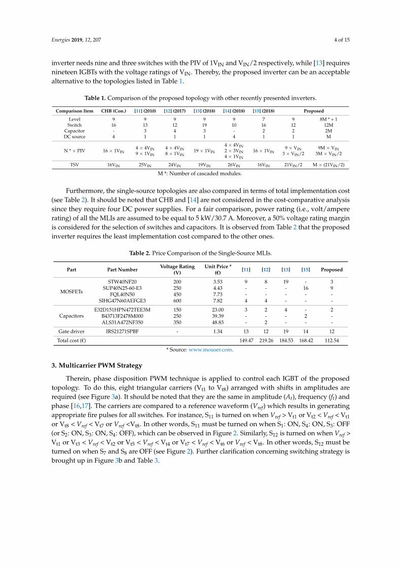
inverter needs nine and three switches with the PIV of 1VIN and VIN/2 respectively, while [13] requiresnineteen IGBTs with the voltage ratings of VIN. Thereby, the proposed inverter can be an acceptablealternative to the topologies listed in Table 1.
Table 1. Comparison of the proposed topology with other recently presented inverters.
Comparison Item CHB (Con.) [11] (2010) [12] (2017) [13] (2018) [14] (2018) [15] (2018) Proposed
Level 9 9 9 9 9 7 9 8M * + 1Switch 16 13 12 19 10 16 12 12M
Capacitor - 3 4 3 - 2 2 2MDC source 4 1 1 1 4 1 1 M
N * × PIV 16 × 1VIN4 × 4VIN9 × 1VIN
4 × 4VIN8 × 1VIN
19 × 1VIN
4 × 4VIN2 × 3VIN4 × 1VIN
16 × 1VIN9 × VIN
3 × VIN/29M × VIN
3M × VIN/2
TSV 16VIN 25VIN 24VIN 19VIN 26VIN 16VIN 21VIN/2 M × (21VIN/2)
M *: Number of cascaded modules.
Furthermore, the single-source topologies are also compared in terms of total implementation cost(see Table 2). It should be noted that CHB and [14] are not considered in the cost-comparative analysissince they require four DC power supplies. For a fair comparison, power rating (i.e., volt/ampererating) of all the MLIs are assumed to be equal to 5 kW/30.7 A. Moreover, a 50% voltage rating marginis considered for the selection of switches and capacitors. It is observed from Table 2 that the proposedinverter requires the least implementation cost compared to the other ones.
Table 2. Price Comparison of the Single-Source MLIs.
Part Part Number Voltage Rating(V)
Unit Price *(€) [11] [12] [13] [15] Proposed
MOSFETs
STW40NF20 200 3.53 9 8 19 - 3SUP40N25-60-E3 250 4.43 - - - 16 9
FQL40N50 450 7.73 - - - - -SIHG47N60AEFGE3 600 7.82 4 4 - - -
CapacitorsE32D151HPN472TEE3M 150 23.00 3 2 4 - 2
B43713F2478M000 250 39.39 - - - 2 -ALS31A472NF350 350 48.83 - 2 - - -
Gate driver IRS21271SPBF - 1.34 13 12 19 14 12
Total cost (€) 149.47 219.26 184.53 168.42 112.54
* Source: www.mouser.com.
3. Multicarrier PWM Strategy
Therein, phase disposition PWM technique is applied to control each IGBT of the proposedtopology. To do this, eight triangular carriers (Vt1 to Vt8) arranged with shifts in amplitudes arerequired (see Figure 3a). It should be noted that they are the same in amplitude (At), frequency (ft) andphase [16,17]. The carriers are compared to a reference waveform (Vref) which results in generatingappropriate fire pulses for all switches. For instance, S11 is turned on when Vref > Vt1 or Vt2 < Vref < Vt1
or Vt8 < Vref < Vt7 or Vref <Vt8. In other words, S11 must be turned on when S1: ON, S4: ON, S3: OFF(or S2: ON, S3: ON, S4: OFF), which can be observed in Figure 2. Similarly, S12 is turned on when Vref >Vt1 or Vt3 < Vref < Vt2 or Vt5 < Vref < Vt4 or Vt7 < Vref < Vt6 or Vref < Vt8. In other words, S12 must beturned on when S7 and S8 are OFF (see Figure 2). Further clarification concerning switching strategy isbrought up in Figure 3b and Table 3.

Energies 2019, 12, 207 5 of 15
Energies 2019, 12, x FOR PEER REVIEW 5 of 15
Vref
Vt3
Vt4
Vt5
Vt6
VIN
VIN/2
0-VIN/2
-VIN
At
2At
-At
-2At
Are f
Vt23At
-3At
Vt7
4At
Vt1
-4At
Vt8
2VIN
3VIN/2
-3VIN/2 -2VIN
t1 t2 t3 t4 t5 t6 t7π t8 t9 t10 t11 t12 2π 0 (a)
Vref
Vt1
Vt2
Vt3
Vt4
Vt5
Vt6
Vt7
Vt8
+- S1
NOT S2
+- AND
+-
+-
OR S3
+-
+-
AND
OR S4
AND
OR S5
ORAND S6
+-
AND
NOT
NOTOR
ANDNOT
NOT
NOT AND
NOT
+-
AND
S7 & S8
NOT
S12
ORNOT
NOT S11
S10NOT S9
(b)
Figure 3. (a) PWM technique, (b) Logic schematic.
Table 3. On-State IGBTs for Each Level.
Relationship between the Carriers and Vref ON-State IGBTs Levels Vref > Vt1 S1-S4-S5-S10-S11-S12 +4VIN
Vt2 < Vref < Vt1 S1-S4-S5-S7-S8-S10-S11 +3VIN Vt3 < Vref < Vt2 S1-S3-S4-S5-S6-S10-S12 +2VIN Vt4 < Vref < Vt3 S1-S3-S5-S7-S8-S10 +1VIN Vt5 < Vref < Vt4 S2-S3-S4-S5-S6-S10-S12 0 Vt6 < Vref < Vt5 S2-S4-S6-S7-S8-S9 −1VIN Vt7 < Vref < Vt6 S2-S3-S4-S5-S6-S9-S12 −2VIN Vt8 < Vref < Vt7 S2-S3-S6-S7-S8-S9-S11 −3VIN
Vref < Vt8 S2-S3-S6-S9-S11-S12 −4VIN
Figure 3. (a) PWM technique, (b) Logic schematic.
Table 3. On-State IGBTs for Each Level.
Relationship between the Carriers and Vref ON-State IGBTs Levels
Vref > Vt1 S1-S4-S5-S10-S11-S12 +4VINVt2 < Vref < Vt1 S1-S4-S5-S7-S8-S10-S11 +3VINVt3 < Vref < Vt2 S1-S3-S4-S5-S6-S10-S12 +2VINVt4 < Vref < Vt3 S1-S3-S5-S7-S8-S10 +1VINVt5 < Vref < Vt4 S2-S3-S4-S5-S6-S10-S12 0Vt6 < Vref < Vt5 S2-S4-S6-S7-S8-S9 −1VINVt7 < Vref < Vt6 S2-S3-S4-S5-S6-S9-S12 −2VINVt8 < Vref < Vt7 S2-S3-S6-S7-S8-S9-S11 −3VIN
Vref < Vt8 S2-S3-S6-S9-S11-S12 −4VIN

Energies 2019, 12, 207 6 of 15
4. Loss Distribution and Thermal Modeling
4.1. Power Loss Analysis
The power loss for a multilevel inverter is composed of three parts including PC, PS and PR whichare elaborated as follows:
4.1.1. Conduction Loss (PC)
PC is caused by parasitic resistance (i.e., ON-state resistance of the switch (RS) and its paralleldiode (RD), capacitor internal resistance (RC)) involved in the current paths [18]. Table 4 shows theequivalent value of the parasitic resistance (Req) existing in each voltage level. It should be noted thatin the present work RS, RD, and RC are considered equal to 0.27 Ω, 0.05 Ω, and 0.03 Ω, respectively.
Table 4. Req in Each Step.
Output Level Req (Ω)
0 2RS + 2RD = 0.64±VIN/2 3RS + 2RD + RC = 0.94±VIN 3RS + RD = 0.86
±3VIN/2 5RS + RD + RC = 1.43±2VIN 6RS + 2RC = 1.68
If |Vref| < At, the output voltage switches between 0 and +VIN/2 (see Figure 3a). Consequently,the output current passes through two switches and two diodes (three switches, two diodes, and onecapacitor) during 0 (+VIN/2) level, as depicted in Table 4. In this case, the energy dissipated within0 < t < t1 (t6 < t < t7 or t12 < t < 2π) is attained by Equation (1) in which At, Aref, and fref are consideredequal to 0.25, 0.9, and 50 Hz, respectively [18]. Moreover, t1 is calculated as follows:
E0&VIN /2 =t1∫0
[ILoadsin
(2π fre f t
)]2
×[(3RS + 2RD + RC)
Are f sin(2π fre f t)At
+(2RS + 2RD)
(1 − Are f sin(2π fre f t)
At
)]dt
= 2.04 × 10⁻⁵ × (Pout/VIN)2
(1)
t1 =sin−1(At/Are f )
2π fre f=
sin−1(0.25/0.9)
100π= 9 × 10⁻⁴sec. (2)
Similarly, the energy losses that occurred in other time intervals are calculated by Equations (3)–(8).
EVIN /2 &VIN =t2∫
t1
[ILoadsin
(2π fre f t
)]2
×[(3RS + RD)
Are f sin(2π fre f t)−AtAt
+(3RS + 2RD + RC)
(1 − Are f sin(2π fre f t)−At
At
)]dt
= 2.03 × 10⁻⁴ × (Pout/VIN)2
(3)
t2 =sin−1(2At/Are f )
2π fre f=
sin−1(0.5/0.9)
100π= 1.87 × 10⁻³sec. (4)
EVIN &3VIN /2 =t3∫
t2
[ILoadsin
(2π fre f t
)]2
×[(5RS + RD + RC)
Are f sin(2π fre f t)−2AtAt
+(3RS + RD)
(1 − Are f sin(2π fre f t)−2At
At
)]dt
= 7.2 × 10⁻⁴ × (Pout/VIN)2
(5)
t3 =sin−1(3At/Are f )
2π fre f=
sin−1(0.75/0.9)
100π= 3.1 × 10⁻³sec. (6)
E3VIN /2 &2VIN =t4∫
t3
[ILoadsin
(2π fre f t
)]2
×[(6RS + 2RC)
Are f sin(2π fre f t)−3AtAt
+(5RS + RD + RC)
(1 − Are f sin(2π fre f t)−3At
At
)]dt
= 0.0051 × (Pout/VIN)2
(7)
Energies 2019, 12, 207 7 of 15
t4 =π − sin−1(3At/Are f )
2π fre f=
π − sin−1(0.75/0.9)
100π= 6.86 × 10⁻³sec. (8)
Due to quarter-wave symmetry of the output voltage, the total conduction loss for the proposed9 L topology is:
PC =(4E0 &VIN /2 + 4EVIN /2 &VIN+ 4EVIN &3VIN /2 + 2E3VIN /2 &2VIN
)× fre f = 0.69 × (Pout/VIN)
2 (9)
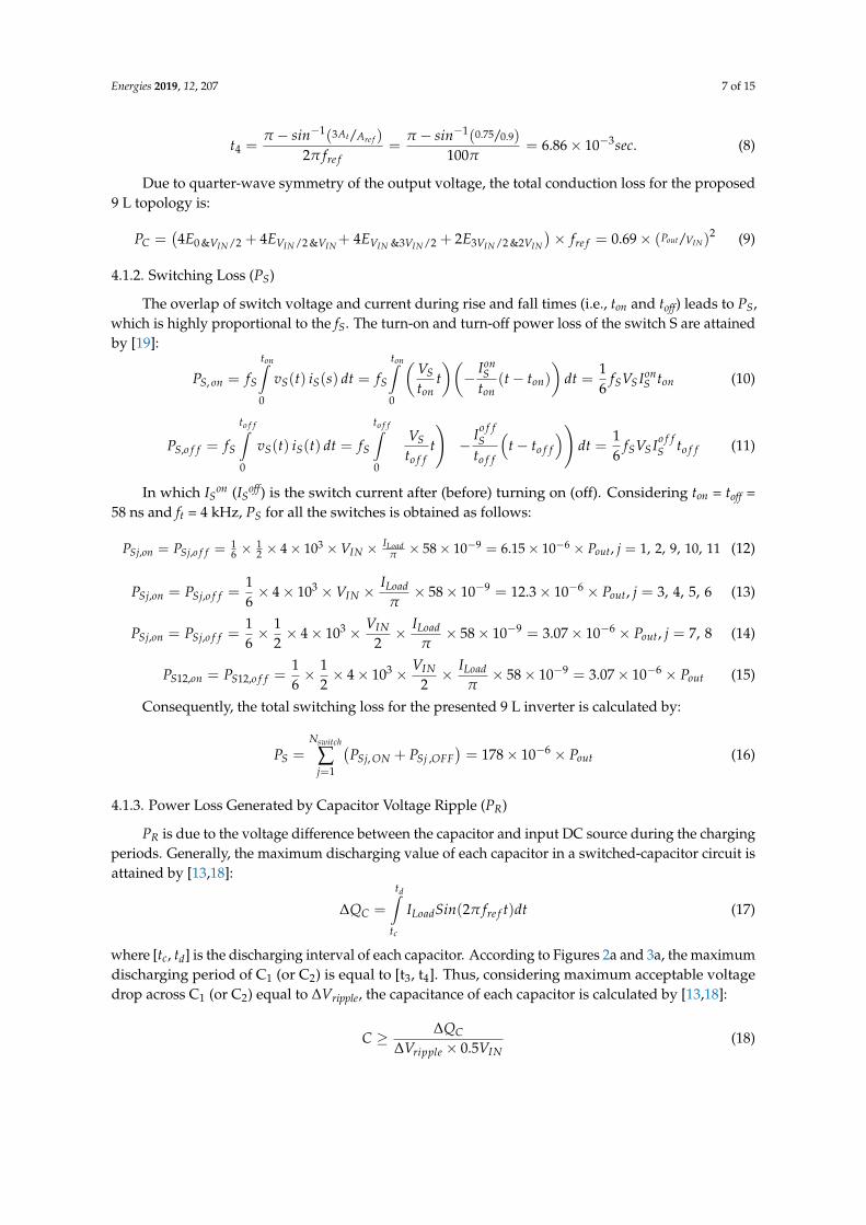
4.1.2. Switching Loss (PS)
The overlap of switch voltage and current during rise and fall times (i.e., ton and toff) leads to PS,which is highly proportional to the fS. The turn-on and turn-off power loss of the switch S are attainedby [19]:
PS, on = fS
ton∫0
vS(t) iS(s) dt = fS
ton∫0
(VSton
t)(
−IonS
ton(t − ton)
)dt =
16
fSVS IonS ton (10)
PS,o f f = fS
to f f∫0
vS(t) iS(t) dt = fS
to f f∫0
(VSto f f
t
)(−
Io f fS
to f f
(t − to f f
))dt =
16
fSVS Io f fS to f f (11)
In which ISon (IS
off) is the switch current after (before) turning on (off). Considering ton = toff =58 ns and ft = 4 kHz, PS for all the switches is obtained as follows:
PSj,on = PSj,o f f =16 × 1
2 × 4 × 103 × VIN × ILoadπ × 58 × 10−9 = 6.15 × 10⁻⁶ × Pout, j = 1, 2, 9, 10, 11 (12)
PSj,on = PSj,o f f =16× 4 × 103 × VIN × ILoad
π× 58 × 10−9 = 12.3 × 10⁻⁶ × Pout, j = 3, 4, 5, 6 (13)
PSj,on = PSj,o f f =16× 1
2× 4 × 103 × VIN
2× ILoad
π× 58 × 10−9 = 3.07 × 10⁻⁶ × Pout, j = 7, 8 (14)
PS12,on = PS12,o f f =16× 1
2× 4 × 103 × VIN
2× ILoad
π× 58 × 10−9 = 3.07 × 10⁻⁶ × Pout (15)
Consequently, the total switching loss for the presented 9 L inverter is calculated by:
PS =Nswitch
∑j=1
(PSj, ON + PSj ,OFF
)= 178 × 10−6 × Pout (16)
4.1.3. Power Loss Generated by Capacitor Voltage Ripple (PR)
PR is due to the voltage difference between the capacitor and input DC source during the chargingperiods. Generally, the maximum discharging value of each capacitor in a switched-capacitor circuit isattained by [13,18]:
∆QC =
td∫tc
ILoadSin(2π fre f t)dt (17)
where [tc, td] is the discharging interval of each capacitor. According to Figures 2a and 3a, the maximumdischarging period of C1 (or C2) is equal to [t3, t4]. Thus, considering maximum acceptable voltagedrop across C1 (or C2) equal to ∆Vripple, the capacitance of each capacitor is calculated by [13,18]:
C ≥ ∆QC∆Vripple × 0.5VIN
(18)

Energies 2019, 12, 207 8 of 15
For example, considering Pout = 1.4 kW (ILoad = 7 A, VIN=200 V) and ∆Vripple = 10%, the capacitancesfor the proposed inverter are obtained as follows:
C1 = C2 =
0.00686∫0.0031
7 × Sin(100πt)dt
0.1 × 100=
0.02410
= 2400 µF (19)
It also should be noted that nominal voltage of the capacitors is equal to VIN/2 (see Figure 2).Consequently, PR for the proposed topology is attained as follows:
PR =fre f2
(2∑
i=1Ci
(∆Vripple × 0.5VIN
)2)= 50 ×
(0.00686∫0.0031
ILoadsin(100πt) dt × ∆Vripple × 0.5VIN
)= 0.088 × ∆Vripple × Pout (20)
Therefore, considering Equations (9), (16), and (20), the efficiency is calculated by Equation (21).
η =Pout
Pin=
Pout
Pout + PC + PS + PR(21)
Theoretical efficiency of the proposed inverter has been calculated at different output power andpresented in Figure 4. It is observed that there is a marked rise in the efficiency by increasing theoutput power.
Energies 2019, 12, x FOR PEER REVIEW 8 of 15
d
c
t
C Load reft
Q I Sin( 2 f t )dtΔ π= (17)
where [tc, td] is the discharging interval of each capacitor. According to Figures 2a and 3a, the maximum discharging period of C1 (or C2) is equal to [t3, t4]. Thus, considering maximum acceptable voltage drop across C1 (or C2) equal to ΔVripple, the capacitance of each capacitor is calculated by [13,18]:
C
ripple IN
QCV 0.5V
ΔΔ
≥×
(18)
For example, considering Pout = 1.4 kW (ILoad = 7 A, VIN=200 V) and ΔVripple = 10%, the capacitances for the proposed inverter are obtained as follows:
0.00686
0.00311 2
7 Sin(100 t )dt0.024C C 2400 F
0.1 100 10
πμ
×= = = =
×
(19)
It also should be noted that nominal voltage of the capacitors is equal to VIN/2 (see Figure 2). Consequently, PR for the proposed topology is attained as follows:
( )0.006862 2ref
R i ripple IN Load ripple IN ripple outi 1 0.0031
fP C V 0.5V 50 I sin(100 t )dt V 0.5V 0.088 V P2 Δ π Δ Δ=
= × = × × × = × × (20)
Therefore, considering Equations (9), (16), and (20), the efficiency is calculated by Equation (21).
out out
in out C S R
P PP P P P P
η = =+ + + (21)
Theoretical efficiency of the proposed inverter has been calculated at different output power and presented in Figure 4. It is observed that there is a marked rise in the efficiency by increasing the output power.
Figure 4. Inverter efficiency at different power output.
4.2. Thermal Model
Heat distribution through semiconductor components is caused by power loss, which leads to an increasing of Tj [20]. This temperature, for safety reasons, should be monitored and kept within a specified range during the inverter operation. Figure 5a illustrates the thermal model implemented for a single semiconductor, in which the thermal impedance between junction and case (Zth) is considered a four-layer foster network (see Figure 5b) [21,22]. It should be noted that Zc and Zs are the thermal impedances from the case to the heat sink and from the heat sink to the ambient, respectively. These are found on the manufacturer datasheet.
84
86
88
90
92
94
96
98
100
0 250 500 750 1000 1250 1500 1750 2000 2250
EFFI
CIEN
CY (%
)
POUT (W)
Figure 4. Inverter efficiency at different power output.
4.2. Thermal Model
Heat distribution through semiconductor components is caused by power loss, which leads toan increasing of Tj [20]. This temperature, for safety reasons, should be monitored and kept within aspecified range during the inverter operation. Figure 5a illustrates the thermal model implemented fora single semiconductor, in which the thermal impedance between junction and case (Zth) is considereda four-layer foster network (see Figure 5b) [21,22]. It should be noted that Zc and Zs are the thermalimpedances from the case to the heat sink and from the heat sink to the ambient, respectively. Theseare found on the manufacturer datasheet.

Energies 2019, 12, 207 9 of 15Energies 2019, 12, x FOR PEER REVIEW 9 of 15
ΔP
Tj Tc Ts TaZth
Cth
Zc Zs
Cs
Semiconductor Semiconductor Case
Heat Sink
(a)
Ta Tc
Tj
Rth1 Rth2 Rth3 Rth4
Zth
Cth1 Cth2 Cth3 Cth4
ΔP
(b)
Figure 5. (a) Semiconductor thermal model; (b) foster network of Zth.
Modelling loss dissipation of the proposed 9 L inverter in MATLAB/Simulink yields the junction temperature of the power electronic devices [23–25]. Herein, Ta is considered equal to 40 °C and the PM75CLA060 switch produced by Mitsubishi Electric is chosen in the thermal estimation.
The estimated Tj of some power switches employed in the proposed inverter at 20 kW output power is illustrated in Figure 6. It can be observed that S12 has the lowest Tj (approximately 43.9 °C), while this temperature approaches 46.7 °C for S11.
Figure 6. The estimated Tj at 20 kW output power.
44
44.5
45
T j, S1
44
44.5
45
T j, S9
46
46.5
47
T j, S11
4 4.1 4.2 4.3 4.4 4.5 4.6 4.7 4.8 4.9 543.5
44
44.5
Time (sec)
T j, S12
Figure 5. (a) Semiconductor thermal model; (b) foster network of Zth.
Modelling loss dissipation of the proposed 9 L inverter in MATLAB/Simulink yields the junctiontemperature of the power electronic devices [23–25]. Herein, Ta is considered equal to 40 C and thePM75CLA060 switch produced by Mitsubishi Electric is chosen in the thermal estimation.
The estimated Tj of some power switches employed in the proposed inverter at 20 kW outputpower is illustrated in Figure 6. It can be observed that S12 has the lowest Tj (approximately 43.9 C),while this temperature approaches 46.7 C for S11.
Energies 2019, 12, x FOR PEER REVIEW 9 of 15
ΔP
Tj Tc Ts TaZth
Cth
Zc Zs
Cs
Semiconductor Semiconductor Case
Heat Sink
(a)
Ta Tc
Tj
Rth1 Rth2 Rth3 Rth4
Zth
Cth1 Cth2 Cth3 Cth4
ΔP
(b)
Figure 5. (a) Semiconductor thermal model; (b) foster network of Zth.
Modelling loss dissipation of the proposed 9 L inverter in MATLAB/Simulink yields the junction temperature of the power electronic devices [23–25]. Herein, Ta is considered equal to 40 °C and the PM75CLA060 switch produced by Mitsubishi Electric is chosen in the thermal estimation.
The estimated Tj of some power switches employed in the proposed inverter at 20 kW output power is illustrated in Figure 6. It can be observed that S12 has the lowest Tj (approximately 43.9 °C), while this temperature approaches 46.7 °C for S11.
Figure 6. The estimated Tj at 20 kW output power.
44
44.5
45
T j, S1
44
44.5
45
T j, S9
46
46.5
47
T j, S11
4 4.1 4.2 4.3 4.4 4.5 4.6 4.7 4.8 4.9 543.5
44
44.5
Time (sec)
T j, S12
Figure 6. The estimated Tj at 20 kW output power.
5. Simulation and Experimental Results
Simulations have been conducted in MATLAB for steady-state and transient modes, as presentedbelow. Figure 7 shows the inverter output voltage/current and capacitors voltage at resistive-inductiveload (ft = 4 kHz, C1 = C2 = 2300 µF, R = 100 Ω, L = 100 mH). These results confirm the flawlessperformance and self-balanced ability of the presented 9 L inverter. Moreover, the value of the inputDC source is selected at 200 V. Thus, the capacitors and output voltages reach 100 V and 400 V,

Energies 2019, 12, 207 10 of 15
respectively. The proposed topology has also been simulated under step change in the load, and theresults are presented in Figure 8. As can be observed, the voltage ripple across the capacitors risespromptly from 3.5% to 7.2% by decreasing the load impedance. Once again, these figures verify theinherent capacitor voltage balancing ability during inverter operation.
Figure 9 shows the voltage waveforms across some power switches employed in the proposedtopology. It is clear that S3, S5, and S11 (also S1, S2, S4, S6, S9 and S10) must withstand voltages equal tothe input DC source (i.e., 200 V). Other switches (S7, S8 and S12), however, block voltages equal to halfthe input DC source (i.e., 100 V). To sum up, unlike topologies with end side H-bridge, none of theswitches required for the proposed inverter tolerate maximum output voltage (i.e., 400 V).
Furthermore, the effect of different modulation indexes and switching frequencies on the operationof the proposed inverter is shown in Figure 10. It is observed that the inverter output voltage haslower THD at higher modulation index (and higher switching frequency). Moreover, the fundamentalcomponent of output voltage is decreased at lower modulation index.
Energies 2019, 12, x FOR PEER REVIEW 10 of 15
5. Simulation and Experimental Results
Simulations have been conducted in MATLAB for steady-state and transient modes, as presented below. Figure 7 shows the inverter output voltage/current and capacitors voltage at resistive-inductive load (ft = 4 kHz, C1 = C2 = 2300 µF, R = 100 Ω, L = 100 mH). These results confirm the flawless performance and self-balanced ability of the presented 9 L inverter. Moreover, the value of the input DC source is selected at 200 V. Thus, the capacitors and output voltages reach 100 V and 400 V, respectively. The proposed topology has also been simulated under step change in the load, and the results are presented in Figure 8. As can be observed, the voltage ripple across the capacitors rises promptly from 3.5% to 7.2% by decreasing the load impedance. Once again, these figures verify the inherent capacitor voltage balancing ability during inverter operation.
Figure 7. Operation of the presented model under constant load.
-400
-200
0
200
400
V Load
(V)
modulation index=0.9
VIN
-4
-2
0
2
4
I Load
(A)
0
2
4
6
8
I Inpu
t (A)
0 96 0 97 0 98 0 99 196
98
100
V C1 (V
)
0.96 0.97 0.98 0.99 196
98
100
Time (sec)
V C2 (V
)
Figure 7. Operation of the presented model under constant load.

Energies 2019, 12, 207 11 of 15Energies 2019, 12, x FOR PEER REVIEW 11 of 15
Figure 8. Operation of the presented model under sudden load reduction.
Figure 9 shows the voltage waveforms across some power switches employed in the proposed topology. It is clear that S3, S5, and S11 (also S1, S2, S4, S6, S9 and S10) must withstand voltages equal to the input DC source (i.e., 200 V). Other switches (S7, S8 and S12), however, block voltages equal to half the input DC source (i.e., 100 V). To sum up, unlike topologies with end side H-bridge, none of the switches required for the proposed inverter tolerate maximum output voltage (i.e., 400 V).
Figure 9. Voltages across the switches.
-400
-200
0
200
400
V Load
(V)
-8
-4
0
4
8
I Load
(A)
R=100 , L=0.1 H R=50 , L=0.05 H
0 8 0 9 1 1 1-8
-4
0
4
8
I Load
(A)
90
95
100
V C1 (V
)
0.8 0.9 1 1.1 1.290
95
100
Time (sec)
V C2 (V
)
0
100
200
V S3 &
VS5
S5
S3
0.96 0.97 0.98 0.99 10
100
200
Time (sec)
V S7 &
VS1
1 S7S11
Load reduction at VLoad=0
Load reduction at VLoad=2VIN
Figure 8. Operation of the presented model under sudden load reduction.
Energies 2019, 12, x FOR PEER REVIEW 11 of 15
Figure 8. Operation of the presented model under sudden load reduction.
Figure 9 shows the voltage waveforms across some power switches employed in the proposed topology. It is clear that S3, S5, and S11 (also S1, S2, S4, S6, S9 and S10) must withstand voltages equal to the input DC source (i.e., 200 V). Other switches (S7, S8 and S12), however, block voltages equal to half the input DC source (i.e., 100 V). To sum up, unlike topologies with end side H-bridge, none of the switches required for the proposed inverter tolerate maximum output voltage (i.e., 400 V).
Figure 9. Voltages across the switches.
-400
-200
0
200
400
V Load
(V)
-8
-4
0
4
8
I Load
(A)
R=100 , L=0.1 H R=50 , L=0.05 H
0 8 0 9 1 1 1-8
-4
0
4
8
I Load
(A)
90
95
100
V C1 (V
)
0.8 0.9 1 1.1 1.290
95
100
Time (sec)
V C2 (V
)
0
100
200
V S3 &
VS5
S5
S3
0.96 0.97 0.98 0.99 10
100
200
Time (sec)
V S7 &
VS1
1 S7S11
Load reduction at VLoad=0
Load reduction at VLoad=2VIN
Figure 9. Voltages across the switches.

Energies 2019, 12, 207 12 of 15
Energies 2019, 12, x FOR PEER REVIEW 12 of 15
Furthermore, the effect of different modulation indexes and switching frequencies on the operation of the proposed inverter is shown in Figure 10. It is observed that the inverter output voltage has lower THD at higher modulation index (and higher switching frequency). Moreover, the fundamental component of output voltage is decreased at lower modulation index.
(a) (b)
Figure 10. The effect of (a) modulation index on the VLoad, (b) switching frequency on the VLoad.
To validate the high performance of the proposed model, a low-power prototype of the proposed inverter has been implemented and tested. Accordingly, a Texas Instruments (TMS320F28335) fixed-point DSP control board generated gate pulses for employed switches (IRFP460 500 V/ 20 A). Moreover, the value of capacitances and input DC source are selected at 2300 µF and 140 V, respectively. Figure 11 illustrates the results obtained from the hardware implementation of the proposed inverter model under steady-state and transient operating conditions. These figures fully confirm the flawless performance of the proposed inverter.
0.96 0.97 0.98 0.99 1-400
-200
0
200
400
V Load
(V)
0 1000 2000 3000 4000 5000 6000 7000 8000 9000 100000
2
4
6
8
10
Frequency (Hz)
Fundamental (50Hz) = 399.5THD= 13.79%
Mag
(% o
f Fun
dam
enta
l)
Ma= 1 fsw= 4 kHz
0.96 0.97 0.98 0.99 1-400
-200
0
200
400
V Load
(V)
0 1000 2000 3000 4000 5000 6000 7000 8000 9000 100000
2
4
6
8
10
Frequency (Hz)
Fundamental (50Hz) = 399.9THD= 13.64%
Mag
(% o
f Fun
dam
enta
l)
Ma= 1 fsw= 7 kHz
0.96 0.97 0.98 0.99 1-400
-200
0
200
400
V Load
(V)
0 1000 2000 3000 4000 5000 6000 7000 8000 9000 100000
5
10
Frequency (Hz)
Fundamental (50Hz) = 319.8THD= 17.29%
Mag
(% o
f Fun
dam
enta
l)
Ma= 0.8 fsw= 4 kHz
0.96 0.97 0.98 0.99 1-400
-200
0
200
400
V Load
(V)
0 1000 2000 3000 4000 5000 6000 7000 8000 9000 100000
2
4
6
8
10
Frequency (Hz)
Fundamental (50Hz) = 399.4THD= 13.75%
Mag
(% o
f Fun
dam
enta
l)
Ma= 1 fsw= 2 kHz
0.96 0.97 0.98 0.99 1-400
-200
0
200
400
V Load
(V)
0 1000 2000 3000 4000 5000 6000 7000 8000 9000 100000
5
10
15
Frequency (Hz)
Fundamental (50Hz) = 280THD= 21.38%
Mag
(% o
f Fun
dam
enta
l)
Ma= 0.7 fsw= 4 kHz
0.96 0.97 0.98 0.99 1-400
-200
0
200
400
V Load
(V)
0 1000 2000 3000 4000 5000 6000 7000 8000 9000 100000
2
4
6
8
10
Frequency (Hz)
Fundamental (50Hz) = 400THD= 14.05%
Mag
(% o
f Fun
dam
enta
l)
Ma= 1 fsw= 1 kHz
Figure 10. The effect of (a) modulation index on the VLoad, (b) switching frequency on the VLoad.
To validate the high performance of the proposed model, a low-power prototype of the proposedinverter has been implemented and tested. Accordingly, a Texas Instruments (TMS320F28335)fixed-point DSP control board generated gate pulses for employed switches (IRFP460 500 V/20 A).Moreover, the value of capacitances and input DC source are selected at 2300 µF and 140 V, respectively.Figure 11 illustrates the results obtained from the hardware implementation of the proposed invertermodel under steady-state and transient operating conditions. These figures fully confirm the flawlessperformance of the proposed inverter.

Energies 2019, 12, 207 13 of 15Energies 2019, 12, x FOR PEER REVIEW 13 of 15
(a)
(b)
Figure 11. Output voltage/current under, (a) constant load; (b) step change in the load.
6. Conclusions
Herein, the operating principle of a new 9 L inverter has been discussed and confirmed experimentally. The comparative analysis depicted that the presented topology not only reduces the number of semiconductors/DC links required for generating a 9 L voltage waveform, but also employs IGBTs with lower PIV. These merits lead to a high compactness and cost reduction of the conversion system. Due to the intrinsic self-voltage balancing ability, there is no need for complex modulation methods. Thereupon, it enjoys simple control and implementation. Furthermore, the theoretical efficiency demonstrated that the presented configuration has higher efficiency by increasing output power (up to 2000 W). Eventually, the feasibility and effectiveness of the proposed model was verified by the simulation and experimental results.
Author Contributions: All authors contributed equally to this work and all authors have read and approved the final manuscript.
Funding: This research received no external funding.
Conflicts of Interest: The authors declare no conflicts of interest.
ZLoad2=ZLoad1 || 75 Ω + 100 mH
ILoad
VLoad
ILoad
ZLoad1=50 Ω + 100 mH
VLoad
Load reduction
Figure 11. Output voltage/current under, (a) constant load; (b) step change in the load.
6. Conclusions
Herein, the operating principle of a new 9 L inverter has been discussed and confirmedexperimentally. The comparative analysis depicted that the presented topology not only reduces thenumber of semiconductors/DC links required for generating a 9 L voltage waveform, but also employsIGBTs with lower PIV. These merits lead to a high compactness and cost reduction of the conversionsystem. Due to the intrinsic self-voltage balancing ability, there is no need for complex modulationmethods. Thereupon, it enjoys simple control and implementation. Furthermore, the theoreticalefficiency demonstrated that the presented configuration has higher efficiency by increasing outputpower (up to 2000 W). Eventually, the feasibility and effectiveness of the proposed model was verifiedby the simulation and experimental results.
Author Contributions: All authors contributed equally to this work and all authors have read and approved thefinal manuscript.
Funding: This research received no external funding.
Conflicts of Interest: The authors declare no conflicts of interest.

Energies 2019, 12, 207 14 of 15
Nomenclature
MLIs Multilevel invertersCHB Cascaded H-bridgeNPC Neutral point clampedFC Flying capacitorTSV Total standing voltage (V)PIV Peak inverse voltage (V)PWM Pulse width modulationDSP Digital signal processorVIN and IIN Input voltage (V) and current (A) of the inverterVLoad and ILoad Maximum load voltage (V) and current (A)Vt Triangular carrier of the PWM modulationVref Reference waveform of the PWM modulationVS and IS Voltage (V) and current (A) of the switch S∆Vripple Voltage ripple across each capacitor (V)∆QC Maximum discharging value of the capacitor CN Number of power switches with the same PIVM Number of cascaded modulesAt and ft Amplitude and frequency of the triangular carriers (Vt)Aref and fref Amplitude and frequency of the reference waveform (Vref)PC Conduction loss (W)PS Switching loss (W)PR Power loss caused by capacitor voltage ripple (W)PS, on and PS, off Turn-on and turn-off power loss of the switch S (W)Pout Inverter output power (W)RS and RD ON-state resistance of the switch S and its parallel diode (Ω)RC Capacitor internal resistance (Ω)Req Equivalent value of the parasitic resistance in each voltage level (Ω)R and L Resistance (Ω) and inductance (H) of the loadton and toff Rise and fall times of the switch S (s)fS Switching frequency (Hz)Tj Semiconductor junction temperature (C)Tc Semiconductor case temperature (C)Ts Heat sink temperature (C)Ta Ambient temperature (C)Zth Thermal impedance between junction and case of the semiconductorZc Thermal impedance between semiconductor case and its heat sinkZs Thermal impedance between heat sink and ambient
References
1. Kouro, S.; Malinowski, M.; Gopakumar, K.; Pou, J.; Franquelo, L.G.; Wu, B.; Rodriguez, J.; Perez, M.A.;Leon, J.I. Recent Advances and Industrial Applications of Multilevel Converters. IEEE Trans. Ind. Electron.2010, 57, 2553–2580. [CrossRef]
2. Yuan, X. Derivation of Voltage Source Multilevel Converter Topologies. IEEE Trans. Ind. Electron. 2017, 64,966–976. [CrossRef]
3. Rodriguez, J.; Franquelo, L.G.; Kouro, S.; Leon, J.I.; Portillo, R.C.; Prats, M.A.M.; Perez, M.A. MultilevelConverters: An Enabling Technology for High-Power Applications. Proc. IEEE 2009, 97, 1786–1817.[CrossRef]
4. Gupta, K.K.; Ranjan, A.; Bhatnagar, P.; Kumar Sahu, L.; Jain, S. Multilevel Inverter Topologies with ReducedDevice Count: A Review. IEEE Trans. Power Electron. 2016, 31, 135–151. [CrossRef]
5. Leon, J.I.; Vazquez, S.; Franquelo, L.G. Multilevel Converters: Control and Modulation Techniques for TheirOperation and Industrial Applications. Proc. IEEE 2017, 105, 2066–2081. [CrossRef]
Energies 2019, 12, 207 15 of 15
6. Akagi, H. Multilevel Converters: Fundamental Circuits and Systems. Proc. IEEE 2017, 105, 2048–2065.[CrossRef]
7. Wu, B.; Narimani, M. Diode-Clamped Multilevel Inverters. In High-Power Converters and AC Drives;Wiley-IEEE Press: New York, NY, USA, 2017.
8. Khounjahan, H.; Abapour, M.; Zare, K. Switched-Capacitor Based Single Source Cascaded H-bridgeMultilevel Inverter Featuring Boosting Ability. IEEE Trans. Power Electron. 2018, 34, 1113–1124. [CrossRef]
9. Lee, S. Single-Stage Switched-Capacitor Module (S3CM) Topology for Cascaded Multilevel Inverter.IEEE Trans. Power Electron. 2018, 33, 8204–8207. [CrossRef]
10. Choi, J.S.; Kang, F.S. Seven-Level PWM Inverter Employing Series-Connected Capacitors Paralleled toa Single DC Voltage Source. IEEE Trans. Ind. Electron. 2015, 62, 3448–3459.
11. Hinago, Y.; Koizumi, H. A Switched-Capacitor Inverter Using Series/Parallel Conversion. IEEE Int. Symp.Circuits Syst. 2010, 62, 3188–3191.
12. Wang, K.; Zheng, Z.; Wei, D.; Fan, B.; Li, Y. Topology and Capacitor Voltage Balancing Control ofa Symmetrical Hybrid Nine-Level Inverter for High-Speed Motor Drives. IEEE Trans. Ind. Appl. 2017,53, 5563–5572. [CrossRef]
13. Taghvaie, A.; Adabi, J.; Rezanejad, M. A Self-Balanced Step-Up Multilevel Inverter Based onSwitched-Capacitor Structure. IEEE Trans. Power Electron. 2018, 33, 199–209. [CrossRef]
14. Lee, S.S.; Sidorov, M.; Lim, C.S.; Idris, N.R.N.; Heng, Y.E. Hybrid Cascaded Multilevel Inverter (HCMLI)With Improved Symmetrical 4-level Submodule. IEEE Trans. Power Electron. 2018, 33, 932–935. [CrossRef]
15. Lee, S.S. A Single-Phase Single-Source 7-Level Inverter with Triple Voltage Boosting Gain. IEEE Access 2018,6, 30005–30011. [CrossRef]
16. McGrath, B.P.; Holmes, D.G. Multicarrier PWM Strategies for Multilevel Inverters. IEEE Trans. Ind. Electron.2002, 49, 858–867. [CrossRef]
17. Mei, J.; Xiao, B.; Shen, K.; Tolbert, L.M.; Zheng, J.Y. Modular Multilevel Inverter with new ModulationMethod and its Application to Photovoltaic Grid-Connected Generator. IEEE Trans. Power Electron. 2013, 28,5063–5073. [CrossRef]
18. Tsunoda, A.; Hinago, Y.; Koizumi, H. Level-and Phase-Shifted PWM for Seven-Level Switched-CapacitorInverter Using Series/Parallel Conversion. IEEE Trans. Ind. Electron. 2014, 61, 4011–4021. [CrossRef]
19. Barzegarkhoo, R.; Moradzadeh, M.; Zamiri, E.; Kojabadi, H.M.; Blaabjerg, F. A new Boost Switched-CapacitorMultilevel Converter with Reduced Circuit Devices. IEEE Trans. Power Electron. 2018, 33, 6738–6754.[CrossRef]
20. Albarbar, A.; Batunlu, C. Thermal Analysis of Power Electronic Devices Used in Renewable Energy Systems;Springer-Cham: Cham, Switzerland, 2018.
21. Ma, K.; Muñoz-Aguilar, R.S.; Rodriguez, P.; Blaabjerg, F. Thermal and Efficiency Analysis of Five-LevelMultilevel-Clamped Multilevel Converter Considering Grid Codes. IEEE Trans. Ind. Appl. 2014, 50, 415–423.
22. Lixiang, W.; McGuire, J.; Lukaszewski, R.A. Analysis of PWM Frequency Control to Improve the Lifetime ofPWM Inverter. IEEE Trans. Ind. Electron. 2011, 47, 922–929. [CrossRef]
23. Ma, K.; Bahman, A.S.; Beczkowski, S.; Blaabjerg, F. Complete Loss and Thermal Model of PowerSemiconductors Including Device Rating Information. IEEE Trans. Power Electron. 2015, 30, 2556–2569.[CrossRef]
24. Rajapakse, A.; Gole, A.; Jayasinghe, R. An Improved Representation of FACTS Controller SemiconductorLosses in EMTP-Type Programs Using Accurate Loss-Power Injection Into Network Solution. IEEE Trans.Power Del. 2009, 24, 381–389. [CrossRef]
25. Tu, Q.; Xu, Z. Power Losses Evaluation for Modular Multilevel Converter with Junction TemperatureFeedback. In Proceedings of the IEEE Power and Energy Society General Meeting, Detroit, MI, USA,24–29 July 2011; pp. 1–7.
© 2019 by the authors. Licensee MDPI, Basel, Switzerland. This article is an open accessarticle distributed under the terms and conditions of the Creative Commons Attribution(CC BY) license (http://creativecommons.org/licenses/by/4.0/).