sam7-la2 development board - olimex
TRANSCRIPT
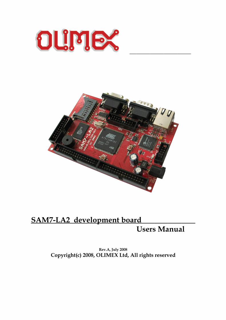
SAM7-LA2 development board Users Manual
Rev.A, July 2008Copyright(c) 2008, OLIMEX Ltd, All rights reserved
INTRODUCTION:
SAM7-LA2 is good platform for low power uC Linux applications. It uses the AT91SAM7A2 MCU which is targeting low power applications. The on board 4MB of RAM and 1 MB of Flash allow RTOS like uclinux, ucos, etc to be used. The CAN , RS232, 100Mbit Ethernet ports allow this board to be used in many applications.
BOARD FEATURES:
− MCU: AT91SAM7A2 16/32-bit ARM7TDMI™ with 16K Bytes RAM, 4x CAN, RTT, 10 bit ADC 348 ksps, 2x UARTs, 2x SPI, 3x 32-bit TIMERS, 4x PWM, SSC, WDT, PDC (DMA) for all peripherals, up to 30MHz operation
− Standard JTAG connector with ARM 2x10 pin layout for programming/debugging with ARM-JTAG
− 4MB SRAM (2MB x 16-bit) PSRAM− 1MB (512K x 16 bit) 55ns MX26LV800BTC FLASH− Ethernet 10/100 with DM9000E + RJ45 connector with two status
LEDs− CAN driver and interface− RS232 driver and interface− SD/MMC card connector− Button− On-board voltage regulator 3.3V with up to 800mA current− Single power supply: 6V AC or DC required, board can take power from
CAN or external pin too− Power supply LED− Power supply filtering capacitor− RESET circuit, RESET button− 6 MHz crystal on socket − 32768 Hz for RTC− Extension headers for all uC ports− PCB: FR-4, 1.5 mm(0.062''), soldermask, silkscreen component print− Dimension: 11 x 80 mm (4.6 x .15'')
ELECTROSTATIC WARNING:
The SAM7-LA2 board is shipped in protective anti-static packaging. The board must not be subject to high electrostatic potentials. General practice for working with static sensitive devices should be applied when working with this board.

BOARD USE REQUIREMENTS:
Cables: You will need different cables depending on the used programming/debugging tool. If you use Olimex's ARM-JTAG, you will need a LPT cable. If you use ARM-USB-OCD or ARM-USB-TINY, you will need USB A-B cable. In the case of ARM-USB-ODC you could also use RS232 cable. You might need other cables in case of other programming/debugging hardware or software tools.
Hardware: Programmer/Debugger – ARM-JTAG, ARM-USB-TINY or ARM-USB-OCD or other compatible programming/debugging tool.
Software: GCC, IAR EWARM or other compatible software platforms.

PROCESSOR FEATURES:
SAM7-LA2 board uses MCU AT91SAM7A2 from Atmel with these features:- ARM7TDMI® ARM® Thumb® Processor Core
o High Performance 32-bit RISCo High-density 16-bit Instruction set (Thumb)o Leader in MIPS/Watto Embedded ICE (In Circuit Emulation)
- 16 Kbytes Internal SRAM- Fully Programmable External Bus Interface (EBI)
o Maximum External Address Space of 6 Mbytes, Up to Four Chip Select Lines
- 8-level Priority, Vectored Interrupt Controllero Three External Interrupts Including One Fast Interrupt Line
- Ten-channel Peripheral Data Controller (PDC)- 57 Programmable I/O Lines- Four 16-bit General Purpose Timers (GPT)
o Three Configurable Modes: Counter, PWM, Captureo Four External Clock Inputs, Three Multi-purpose I/O Pins per
Timer- Four 16-bit Simple Timers (ST)- Four Channel 16-bit Pulse Width Modulation (PWM)- Four CAN Controllers 2.0A and 2.0B Full CAN
o One with 32 Buffers, Three with 16 Buffers- Two USARTs
o Support for J1587 and LIN Protocols- One Master/Slave SPI Interface
o 8 to 16-bit Programmable Data Lengtho Four External Serial Peripheral Chip Selects
- Two 8-channel 10-bit Analog to Digital Converters (ADC)- Two 16-bit Capture Modules (CAPT)- Programmable Watch Timer (WT)- Programmable Watchdog (WD)- Power Management Controller (PMC)
o 32 kHz Oscillator, Main Oscillator and PLL- IEEE 1149.1 JTAG Boundary-scan on all Digital Pins- Fully Static Operation: 0 Hz to 30 MHz at VDDCORE = 3.3V, 85°C- 3.0V to 5.5V Operating Voltage Range- 3.0V to 3.6V Core, Memory and Analog Voltage Range- -40° to +85°C Operating Temperature Range- Available in a 176-lead LQFP Package

BLOCK DIAGRAM:

MEMORY MAP:


SCHEMATIC:
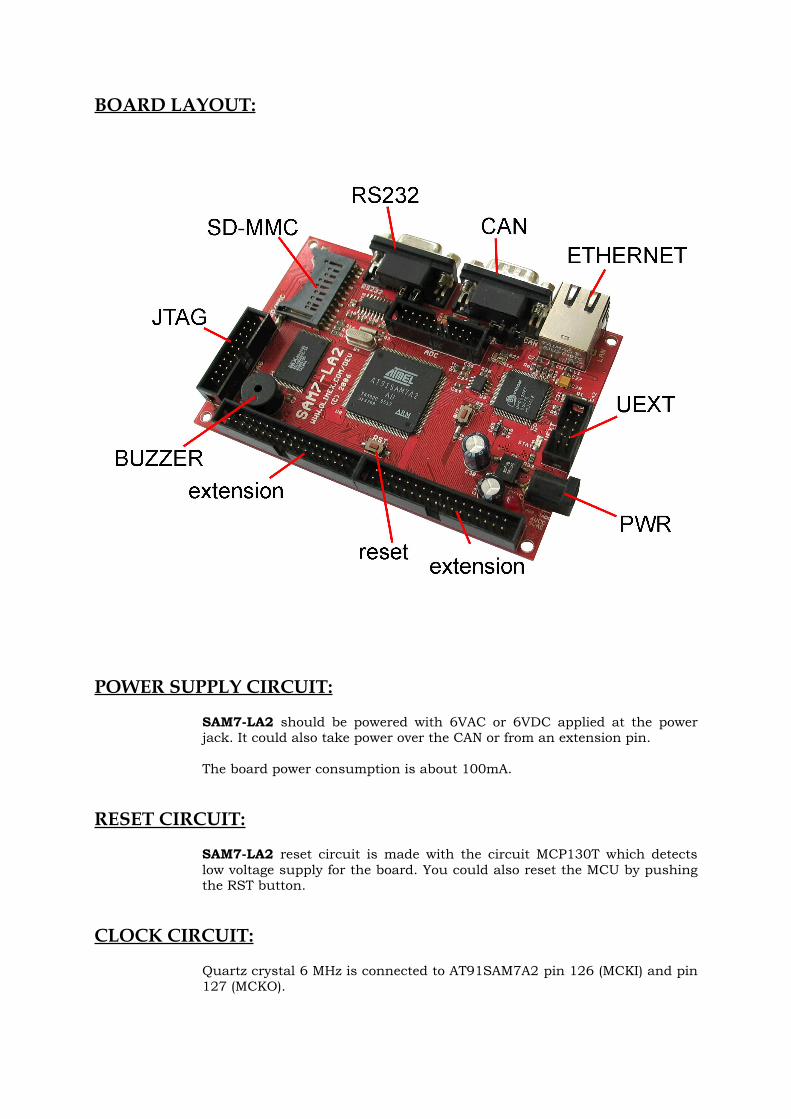
BOARD LAYOUT:
POWER SUPPLY CIRCUIT:
SAM7-LA2 should be powered with 6VAC or 6VDC applied at the power jack. It could also take power over the CAN or from an extension pin.
The board power consumption is about 100mA.
RESET CIRCUIT:
SAM7-LA2 reset circuit is made with the circuit MCP130T which detects low voltage supply for the board. You could also reset the MCU by pushing the RST button.
CLOCK CIRCUIT:
Quartz crystal 6 MHz is connected to AT91SAM7A2 pin 126 (MCKI) and pin 127 (MCKO).

Quartz crystal 32.768 kHz is connected to AT91SAM7A2 pin 113 (RTCKI) and pin 114 (RTCKO) and supplies the Real Time Clock.
JUMPER DESCRIPTION:
DUP/SPEEDWhen 1-2 are shorted, DM9000E pin 60 (#SPEED) is
connected to KG pin of the LAN connector. When 2-3 are shorted, DM9000E pin 61 (#DUP) is connected to KG pin of the LAN connector.
Default position is 1-2 shorted.
CAN_T_EThis jumper assures correct work of the CAN. At each end of
the bus it should be closed. This means that if you have only two devices with CAN, the jumpers of both devices should be closed. If you have more than two devices, only the two end-devices should be closed.
Default state is closed.
CAN_DIf you put this jumper, you disable the CAN interface.Default state is open.
TESTIf you put this jumper, you enable TEST mode for the MCU.
Default state is open.
BDSBoundary Scan. If you put this jumper, you enable the JTAG
boundary scan.Default state is open.
INPUT/OUTPUT:
Button with name BUT, connected to AT91SAM7A2 pin 3 (IRQ1). Reset button with name RST, connected to AT91SAM7A2 pin 39 (NRESET).User status LED with name STAT, connected to AT91SAM7A2 pin 42 (UPIO2).Power-on LED with name PWR showing that 3.3V voltage is available. Buzzer PB1221 connected to AT91SAM7A2 pin 87 (PWM3).
EXTERNAL CONNECTORS DESCRIPTION:
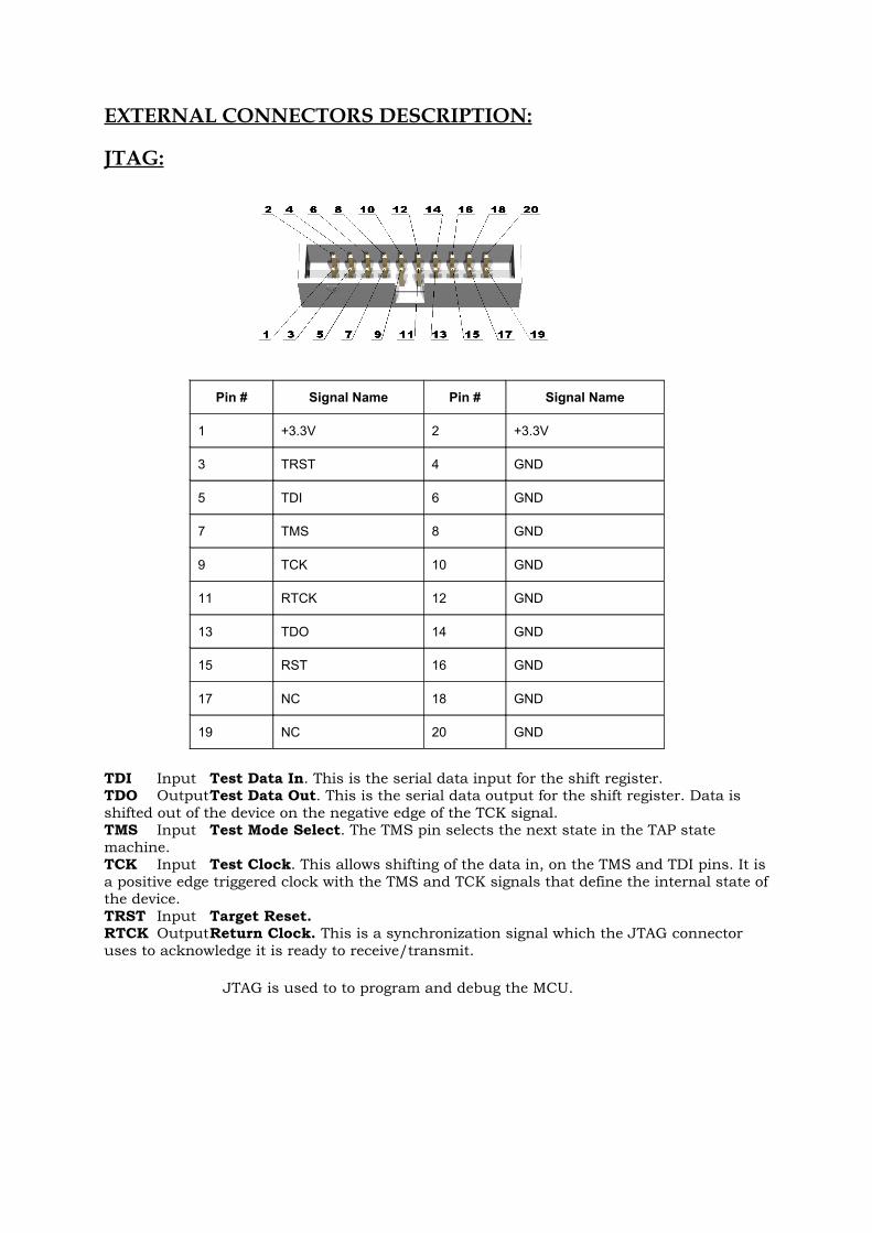
JTAG:
Pin # Signal Name Pin # Signal Name
1 +3.3V 2 +3.3V
3 TRST 4 GND
5 TDI 6 GND
7 TMS 8 GND
9 TCK 10 GND
11 RTCK 12 GND
13 TDO 14 GND
15 RST 16 GND
17 NC 18 GND
19 NC 20 GND
TDI Input Test Data In. This is the serial data input for the shift register.TDO OutputTest Data Out. This is the serial data output for the shift register. Data is shifted out of the device on the negative edge of the TCK signal.TMS Input Test Mode Select. The TMS pin selects the next state in the TAP state machine.TCK Input Test Clock. This allows shifting of the data in, on the TMS and TDI pins. It is a positive edge triggered clock with the TMS and TCK signals that define the internal state of the device.TRST Input Target Reset. RTCK OutputReturn Clock. This is a synchronization signal which the JTAG connector uses to acknowledge it is ready to receive/transmit.
JTAG is used to to program and debug the MCU.

ADC:
Pin # Signal Name Pin # Signal Name
1 ANA0IN0 2 ANA0IN1
3 ANA0IN2 4 ANA0IN3
5 ANA0IN4 6 ANA0IN5
7 ANA0IN6 8 ANA0IN7
9 VREFP0 10 GND
11 +3.3V 12 ANA1IN0
13 ANA1IN1 14 ANA1IN2
15 ANA1IN3 16 ANA1IN4
17 ANA1IN5 18 ANA1IN6
19 ANA1IN7 20 VREFP1
UEXT:
Pin # Signal Name
1 +3.3V
2 GND
3 TXD1
4 RXD1
5 NPCS3
6 NPCS0
7 MISO
8 MOSI
9 SPCK
10 NPCS2
TXD1 OutputTransmit Data 1. This is the asynchronous serial data output 1 (RS232) for the UART controller.RXD1 Input Receive Data 1. This is the asynchronous serial data input 1 (RS232) for the UART controller.NPCS3OutputSPI Chip Select 3. NPCS0OutputSPI Chip Select 0.MISO I/O Master In Slave Out. SPI data transfer signal. It is either input or output depending on whether the MCU is master or slave.MOSI I/O Master Out Slave In. SPI data transfer signal. It is either input or output depending on whether the MCU is master or slave.NPCS2OutputSPI Chip Select 2.
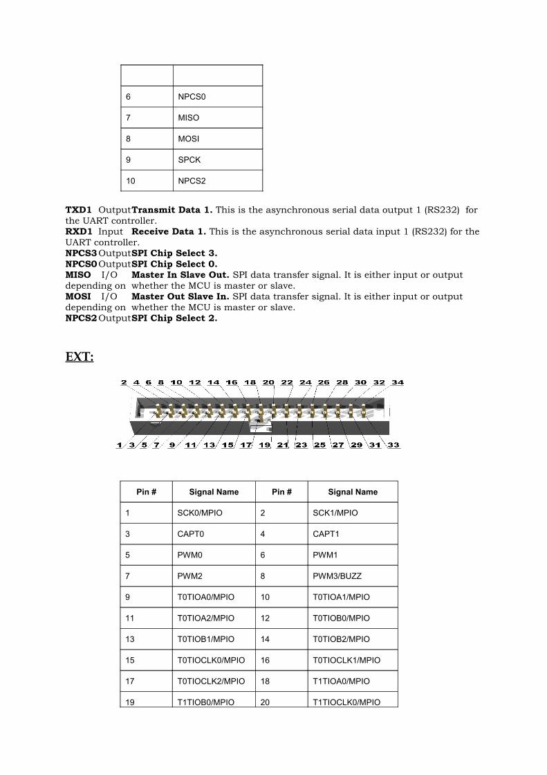
EXT:
Pin # Signal Name Pin # Signal Name
1 SCK0/MPIO 2 SCK1/MPIO
3 CAPT0 4 CAPT1
5 PWM0 6 PWM1
7 PWM2 8 PWM3/BUZZ
9 T0TIOA0/MPIO 10 T0TIOA1/MPIO
11 T0TIOA2/MPIO 12 T0TIOB0/MPIO
13 T0TIOB1/MPIO 14 T0TIOB2/MPIO
15 T0TIOCLK0/MPIO 16 T0TIOCLK1/MPIO
17 T0TIOCLK2/MPIO 18 T1TIOA0/MPIO
19 T1TIOB0/MPIO 20 T1TIOCLK0/MPIO

21 IRQ1/BUT 22 FIQ
23 CANRX1 24 CANTX1
25 CANRX2 26 CANTX2
27 CANRX3 28 CANTX3
29 RST 30 TX1OUT
31 RX1IN 32 VIN
33 +3.3V 34 GND
CANRX1 Input CAN Receive Data 1. CANTX1 Output CAN Transmit Data 1. CANRX2 Input CAN Receive Data 2. CANTX2 Output CAN Transmit Data 2. CANRX3 Input CAN Receive Data 3. CANTX3 Output CAN Transmit Data 3. TX1OUT Output Transmit Data 1. This is the asynchronous serial data output 1 (RS232) after the UART controller.RX1IN Input Receive Data 1. This is the asynchronous serial data input 1 (RS232) before the UART controller.
UPIO:
Pin # Signal Name Pin # Signal Name
1 UPIO0/WP 2 UPIO1/CP
3 UPIO2 4 UPIO3/LAN_RST
5 UPIO4 6 UPIO5
7 UPIO6 8 UPIO7
9 UPIO8 10 UPIO9
11 UPIO10 12 UPIO11
13 UPIO12 14 UPIO13
15 UPIO14 16 UPIO15

17 UPIO16 18 UPIO17
19 UPIO18 20 UPIO19
21 UPIO20 22 UPIO21
23 UPIO22 24 UPIO23
25 UPIO24 26 UPIO25
27 UPIO26 28 UPIO27
29 UPIO28 30 UPIO29
31 UPIO30/IOWAIT 32 UPIO31
33 +3.3V 34 GND
RS232:
Pin # Signal Name
1 NC
2 TXD0
3 RXD0
4 NC
5 GND
6 NC
7 NC
8 NC
9 NC
TXD0 OutputTransmit Data. This is the asynchronous serial data output (RS232) for the shift register on the UART controller.RXD0 Input Receive Data. This is the asynchronous serial data input (RS232) for the shift register on the UART controller.
CAN:
Pin # Signal Name
1 NC

2 CANL
3 GND
4 NC
5 NC
6 GND
7 CANH
8 NC
9 VIN
CANL and CANH are either deferential input, or differential output depending on the function of the SN65HVD230 CAN controller (receiving or transmitting data). VIN is voltage input and through this pin the board could be power-supplied.
LAN :
Pin # Signal Name Chip Side Pin # Signal Name Chip Side
1 TD+ 5 Not Connected (NC)
2 TD- 6 Not Connected (NC)
3 3.3V 7 RD+
4 Not Connected (NC) 8 RD-
LED Color Usage
Right Yellow Activity
Left Green 100MBits/s (Half/Full duplex)

TD- OutputDifferential signal output.TD+ OutputDifferential signal output. RD- Input Differential signal input.RD+ InputDifferential signal input.
SD/MMC card slot:
Pin # Signal Name Pin # Signal Name
1 NPCS1 2 MOSI
3 GND 4 +3.3V
5 SPCK 6 GND
7 MISO 8 +3.3V
9 +3.3V 10 WP
11 - 12 -
13 +3.3V 14 +3.3V
15 CP
NPCS1 OutputSPI Chip Select 1. The signal on this pin enables or disables the SD/MMC.MOSI OutputMaster Out Slave In. As the access to the memory is via SPI interface, this is data output from the MCU (which is master) and input for the memory card (which is slave).SPCK OutputSerial (Synchronization) Clock. This is the synchronization clock for the data transfer. MISO Input Master In Slave Out. As the access to the memory card is via SPI interface, this is data input for the MCU(which is master) and data output from the memory card (which is slave). WP Input Write Protect. This signal is input for the MCU.CP Input Card Present. This signal is input for the MCU.

PWR:Pin # Signal Name
1 PWR
2 GND
At the PWR pin should be applied voltage 4.5VAC or +6VDC.

MECHANICAL DIMENSIONS:
All measures are in Inches.
AVAILABLE DEMO SOFTWARE :
You could find information about SAM7-LA2 demo software on www.olimex.com/dev .

ORDER CODE:SAM7-LA2 – assembled and tested (no kit, no soldering required)
How to order? You can order to us directly or by any of our distributors. Check our web www.olimex.com/dev for more info.
All boards produced by Olimex are RoHS compliant
Revision history:
REV.A - created July 2008

Disclaimer: © 2008 Olimex Ltd. All rights reserved. Olimex®, logo and combinations thereof, are registered trademarks of Olimex Ltd. Other terms and product names may be trademarks of others.The information in this document is provided in connection with Olimex products. No license, express or implied or otherwise, to any intellectual property right is granted by this document or in connection with the sale of Olimex products. Neither the whole nor any part of the information contained in or the product described in this document may be adapted or reproduced in any material from except with the prior written permission of the copyright holder.The product described in this document is subject to continuous development and improvements. All particulars of the product and its use contained in this document are given by OLIMEX in good faith. However all warranties implied or expressed including but not limited to implied warranties of merchantability or fitness for purpose are excluded.This document is intended only to assist the reader in the use of the product. OLIMEX Ltd. shall not be liable for any loss or damage arising from the use of any information in this document or any error or omission in such information or any incorrect use of the product.