sc28l202 dual universal asynchronous …philips semiconductors product data sheet sc28l202 dual...
TRANSCRIPT

SC28L202Dual universal asynchronousreceiver/transmitter (DUART)
Product data sheetSupersedes data of 2004 Apr 16
2005 Nov 01
INTEGRATED CIRCUITS

Philips Semiconductors Product data sheet
SC28L202Dual universal asynchronous receiver/transmitter(DUART)
2005 Nov 01 i
DESCRIPTION 1. . . . . . . . . . . . . . . . . . . . . . . . . . . . . . . . . . . . . . . . . . . . . . . . . . . . . . . . . . . . . . . . . . . . . . . . . . . . . . . . . . . . . . . . . . . . . . . . . . . . . . .
FEATURES 1. . . . . . . . . . . . . . . . . . . . . . . . . . . . . . . . . . . . . . . . . . . . . . . . . . . . . . . . . . . . . . . . . . . . . . . . . . . . . . . . . . . . . . . . . . . . . . . . . . . . . . . . . .
ORDERING INFORMATION 2. . . . . . . . . . . . . . . . . . . . . . . . . . . . . . . . . . . . . . . . . . . . . . . . . . . . . . . . . . . . . . . . . . . . . . . . . . . . . . . . . . . . . . . . . . . .
PIN CONFIGURATIONS 2. . . . . . . . . . . . . . . . . . . . . . . . . . . . . . . . . . . . . . . . . . . . . . . . . . . . . . . . . . . . . . . . . . . . . . . . . . . . . . . . . . . . . . . . . . . . . . .
PIN CONFIGURATION FOR 80XXX BUS INTERFACE (INTEL) 3. . . . . . . . . . . . . . . . . . . . . . . . . . . . . . . . . . . . . . . . . . . . . . . . . . . . . . . . . . . . .
CONFIGURATION FOR 68XXX BUS INTERFACE (MOTOROLA) 4. . . . . . . . . . . . . . . . . . . . . . . . . . . . . . . . . . . . . . . . . . . . . . . . . . . . . . . . . . .
OVERALL DESCRIPTION 5. . . . . . . . . . . . . . . . . . . . . . . . . . . . . . . . . . . . . . . . . . . . . . . . . . . . . . . . . . . . . . . . . . . . . . . . . . . . . . . . . . . . . . . . . . . . .
BRIEF DESCRIPTION OF FUNCTIONAL BLOCKS 5. . . . . . . . . . . . . . . . . . . . . . . . . . . . . . . . . . . . . . . . . . . . . . . . . . . . . . . . . . . . . . . . . . . . . Bus Interface 5. . . . . . . . . . . . . . . . . . . . . . . . . . . . . . . . . . . . . . . . . . . . . . . . . . . . . . . . . . . . . . . . . . . . . . . . . . . . . . . . . . . . . . . . . . . . . . . . . . . Timing Circuits 5. . . . . . . . . . . . . . . . . . . . . . . . . . . . . . . . . . . . . . . . . . . . . . . . . . . . . . . . . . . . . . . . . . . . . . . . . . . . . . . . . . . . . . . . . . . . . . . . . . I/O ports 5. . . . . . . . . . . . . . . . . . . . . . . . . . . . . . . . . . . . . . . . . . . . . . . . . . . . . . . . . . . . . . . . . . . . . . . . . . . . . . . . . . . . . . . . . . . . . . . . . . . . . . . UARTs 5. . . . . . . . . . . . . . . . . . . . . . . . . . . . . . . . . . . . . . . . . . . . . . . . . . . . . . . . . . . . . . . . . . . . . . . . . . . . . . . . . . . . . . . . . . . . . . . . . . . . . . . . . Transmitters and Receivers 5. . . . . . . . . . . . . . . . . . . . . . . . . . . . . . . . . . . . . . . . . . . . . . . . . . . . . . . . . . . . . . . . . . . . . . . . . . . . . . . . . . . . . . . Character and Address Recognition 6. . . . . . . . . . . . . . . . . . . . . . . . . . . . . . . . . . . . . . . . . . . . . . . . . . . . . . . . . . . . . . . . . . . . . . . . . . . . . . . . Flow Control 6. . . . . . . . . . . . . . . . . . . . . . . . . . . . . . . . . . . . . . . . . . . . . . . . . . . . . . . . . . . . . . . . . . . . . . . . . . . . . . . . . . . . . . . . . . . . . . . . . . . . Test Modes and Software 6. . . . . . . . . . . . . . . . . . . . . . . . . . . . . . . . . . . . . . . . . . . . . . . . . . . . . . . . . . . . . . . . . . . . . . . . . . . . . . . . . . . . . . . . .
DETAILED DESCRIPTIONS 6. . . . . . . . . . . . . . . . . . . . . . . . . . . . . . . . . . . . . . . . . . . . . . . . . . . . . . . . . . . . . . . . . . . . . . . . . . . . . . . . . . . . . . . . . Bus Interface 6. . . . . . . . . . . . . . . . . . . . . . . . . . . . . . . . . . . . . . . . . . . . . . . . . . . . . . . . . . . . . . . . . . . . . . . . . . . . . . . . . . . . . . . . . . . . . . . . . . . Timing Circuit 7. . . . . . . . . . . . . . . . . . . . . . . . . . . . . . . . . . . . . . . . . . . . . . . . . . . . . . . . . . . . . . . . . . . . . . . . . . . . . . . . . . . . . . . . . . . . . . . . . . . I/O Ports 8. . . . . . . . . . . . . . . . . . . . . . . . . . . . . . . . . . . . . . . . . . . . . . . . . . . . . . . . . . . . . . . . . . . . . . . . . . . . . . . . . . . . . . . . . . . . . . . . . . . . . . .
UART Operation 8. . . . . . . . . . . . . . . . . . . . . . . . . . . . . . . . . . . . . . . . . . . . . . . . . . . . . . . . . . . . . . . . . . . . . . . . . . . . . . . . . . . . . . . . . . . . . . . . . . . Receiver Operation 9. . . . . . . . . . . . . . . . . . . . . . . . . . . . . . . . . . . . . . . . . . . . . . . . . . . . . . . . . . . . . . . . . . . . . . . . . . . . . . . . . . . . . . . . . . . . . . Arbitrating Interrupt Structure 12. . . . . . . . . . . . . . . . . . . . . . . . . . . . . . . . . . . . . . . . . . . . . . . . . . . . . . . . . . . . . . . . . . . . . . . . . . . . . . . . . . . . . .
PROGRAMMING THE HOST INTERFACE 17. . . . . . . . . . . . . . . . . . . . . . . . . . . . . . . . . . . . . . . . . . . . . . . . . . . . . . . . . . . . . . . . . . . . . . . . . . . . . . .
REGISTER DESCRIPTION AND PROGRAMMING NOTE 18. . . . . . . . . . . . . . . . . . . . . . . . . . . . . . . . . . . . . . . . . . . . . . . . . . . . . . . . . . . . . . . . . .
Registers that control Global Properties of the 28L202 18. . . . . . . . . . . . . . . . . . . . . . . . . . . . . . . . . . . . . . . . . . . . . . . . . . . . . . . . . . . . . . . . . . . GCCR – Global Configuration Control Register 18. . . . . . . . . . . . . . . . . . . . . . . . . . . . . . . . . . . . . . . . . . . . . . . . . . . . . . . . . . . . . . . . . . . . . . GCCR(7:6) DACKN Assertion 18. . . . . . . . . . . . . . . . . . . . . . . . . . . . . . . . . . . . . . . . . . . . . . . . . . . . . . . . . . . . . . . . . . . . . . . . . . . . . . . . . . . . . GCCR(5:3): Reserved 18. . . . . . . . . . . . . . . . . . . . . . . . . . . . . . . . . . . . . . . . . . . . . . . . . . . . . . . . . . . . . . . . . . . . . . . . . . . . . . . . . . . . . . . . . . . . GCCR(2:1): Interrupt vector configuration 18. . . . . . . . . . . . . . . . . . . . . . . . . . . . . . . . . . . . . . . . . . . . . . . . . . . . . . . . . . . . . . . . . . . . . . . . . . . GCCR(0): Interrupt Status Masking 18. . . . . . . . . . . . . . . . . . . . . . . . . . . . . . . . . . . . . . . . . . . . . . . . . . . . . . . . . . . . . . . . . . . . . . . . . . . . . . . . SFSR A and B Special Feature & Status Register 19. . . . . . . . . . . . . . . . . . . . . . . . . . . . . . . . . . . . . . . . . . . . . . . . . . . . . . . . . . . . . . . . . . . . SFSR(7:4) Reserved 19. . . . . . . . . . . . . . . . . . . . . . . . . . . . . . . . . . . . . . . . . . . . . . . . . . . . . . . . . . . . . . . . . . . . . . . . . . . . . . . . . . . . . . . . . . . . . SFSR(3) Status of loop back error check. 19. . . . . . . . . . . . . . . . . . . . . . . . . . . . . . . . . . . . . . . . . . . . . . . . . . . . . . . . . . . . . . . . . . . . . . . . . . . SFSR(0) Reserved 19. . . . . . . . . . . . . . . . . . . . . . . . . . . . . . . . . . . . . . . . . . . . . . . . . . . . . . . . . . . . . . . . . . . . . . . . . . . . . . . . . . . . . . . . . . . . . . TRR Test and Revision Register. 19. . . . . . . . . . . . . . . . . . . . . . . . . . . . . . . . . . . . . . . . . . . . . . . . . . . . . . . . . . . . . . . . . . . . . . . . . . . . . . . . . . TRR[7] Test 2 Enable 19. . . . . . . . . . . . . . . . . . . . . . . . . . . . . . . . . . . . . . . . . . . . . . . . . . . . . . . . . . . . . . . . . . . . . . . . . . . . . . . . . . . . . . . . . . . . TRR[6:0] – Chip Revision Code 19. . . . . . . . . . . . . . . . . . . . . . . . . . . . . . . . . . . . . . . . . . . . . . . . . . . . . . . . . . . . . . . . . . . . . . . . . . . . . . . . . . . STCR – Scan Test Control Register. 19. . . . . . . . . . . . . . . . . . . . . . . . . . . . . . . . . . . . . . . . . . . . . . . . . . . . . . . . . . . . . . . . . . . . . . . . . . . . . . . SES – System Enable Status Register, A and B 19. . . . . . . . . . . . . . . . . . . . . . . . . . . . . . . . . . . . . . . . . . . . . . . . . . . . . . . . . . . . . . . . . . . . . EOS – Enhanced Operation Status Register 19. . . . . . . . . . . . . . . . . . . . . . . . . . . . . . . . . . . . . . . . . . . . . . . . . . . . . . . . . . . . . . . . . . . . . . . .
UART Registers 20. . . . . . . . . . . . . . . . . . . . . . . . . . . . . . . . . . . . . . . . . . . . . . . . . . . . . . . . . . . . . . . . . . . . . . . . . . . . . . . . . . . . . . . . . . . . . . . . . . . . These registers are generally concerned with formatting, transmitting and receiving data. 20. . . . . . . . . . . . . . . . . . . . . . . . . . . . . . . . . . MR0 – Mode Register 0, A and B 20. . . . . . . . . . . . . . . . . . . . . . . . . . . . . . . . . . . . . . . . . . . . . . . . . . . . . . . . . . . . . . . . . . . . . . . . . . . . . . . . . . MR0[7] Fixed length Watchdog Timer 20. . . . . . . . . . . . . . . . . . . . . . . . . . . . . . . . . . . . . . . . . . . . . . . . . . . . . . . . . . . . . . . . . . . . . . . . . . . . . . MR0[5:4] – Tx interrupt fill level. 20. . . . . . . . . . . . . . . . . . . . . . . . . . . . . . . . . . . . . . . . . . . . . . . . . . . . . . . . . . . . . . . . . . . . . . . . . . . . . . . . . . . MR0[3] – FIFO Size 20. . . . . . . . . . . . . . . . . . . . . . . . . . . . . . . . . . . . . . . . . . . . . . . . . . . . . . . . . . . . . . . . . . . . . . . . . . . . . . . . . . . . . . . . . . . . . . MR0[2:0] – Legacy Baud Rate Group Selection 20. . . . . . . . . . . . . . . . . . . . . . . . . . . . . . . . . . . . . . . . . . . . . . . . . . . . . . . . . . . . . . . . . . . . . . MR1 – Mode Register 1, A and B 21. . . . . . . . . . . . . . . . . . . . . . . . . . . . . . . . . . . . . . . . . . . . . . . . . . . . . . . . . . . . . . . . . . . . . . . . . . . . . . . . . . MR1[7] – Receiver Request to Send (hardware flow control) 21. . . . . . . . . . . . . . . . . . . . . . . . . . . . . . . . . . . . . . . . . . . . . . . . . . . . . . . . . . . MR1[6] – Receiver interrupt control bit 1. 21. . . . . . . . . . . . . . . . . . . . . . . . . . . . . . . . . . . . . . . . . . . . . . . . . . . . . . . . . . . . . . . . . . . . . . . . . . . . MR1 [5] – Error Mode Select and sub modes 21. . . . . . . . . . . . . . . . . . . . . . . . . . . . . . . . . . . . . . . . . . . . . . . . . . . . . . . . . . . . . . . . . . . . . . . . MR1[4:3] – Parity Mode Select 21. . . . . . . . . . . . . . . . . . . . . . . . . . . . . . . . . . . . . . . . . . . . . . . . . . . . . . . . . . . . . . . . . . . . . . . . . . . . . . . . . . . . MR1[2] – Parity Type Select 21. . . . . . . . . . . . . . . . . . . . . . . . . . . . . . . . . . . . . . . . . . . . . . . . . . . . . . . . . . . . . . . . . . . . . . . . . . . . . . . . . . . . . . . MR1[1:0] – Bits per Character Select 21. . . . . . . . . . . . . . . . . . . . . . . . . . . . . . . . . . . . . . . . . . . . . . . . . . . . . . . . . . . . . . . . . . . . . . . . . . . . . . . MR2 – Mode Register 2, A and B 22. . . . . . . . . . . . . . . . . . . . . . . . . . . . . . . . . . . . . . . . . . . . . . . . . . . . . . . . . . . . . . . . . . . . . . . . . . . . . . . . . . MR2[7:6] – Mode Select 22. . . . . . . . . . . . . . . . . . . . . . . . . . . . . . . . . . . . . . . . . . . . . . . . . . . . . . . . . . . . . . . . . . . . . . . . . . . . . . . . . . . . . . . . . . MR2[7:6] = b’00 Normal Mode 22. . . . . . . . . . . . . . . . . . . . . . . . . . . . . . . . . . . . . . . . . . . . . . . . . . . . . . . . . . . . . . . . . . . . . . . . . . . . . . . . . . . . . MR2[7:6] = b’01 Automatic Echo 22. . . . . . . . . . . . . . . . . . . . . . . . . . . . . . . . . . . . . . . . . . . . . . . . . . . . . . . . . . . . . . . . . . . . . . . . . . . . . . . . . . . MR2[7:6] = b’10 selects local loop back diagnostic mode. In this mode: 22. . . . . . . . . . . . . . . . . . . . . . . . . . . . . . . . . . . . . . . . . . . . . . . . . MR2 [7:6] = b’11 Selects the Remote Loop back diagnostic mode. In this mode: 22. . . . . . . . . . . . . . . . . . . . . . . . . . . . . . . . . . . . . . . . . . MR2[5] Transmitter Request to Send Control 22. . . . . . . . . . . . . . . . . . . . . . . . . . . . . . . . . . . . . . . . . . . . . . . . . . . . . . . . . . . . . . . . . . . . . . . . MR2[4] – Clear to Send Control 22. . . . . . . . . . . . . . . . . . . . . . . . . . . . . . . . . . . . . . . . . . . . . . . . . . . . . . . . . . . . . . . . . . . . . . . . . . . . . . . . . . . MR2[3:0] – Stop Bit Length Select 22. . . . . . . . . . . . . . . . . . . . . . . . . . . . . . . . . . . . . . . . . . . . . . . . . . . . . . . . . . . . . . . . . . . . . . . . . . . . . . . . .

Philips Semiconductors Product data sheet
SC28L202Dual universal asynchronous receiver/transmitter(DUART)
2005 Nov 01 ii
MR3 – Mode Register 3, A and B 23. . . . . . . . . . . . . . . . . . . . . . . . . . . . . . . . . . . . . . . . . . . . . . . . . . . . . . . . . . . . . . . . . . . . . . . . . . . . . . . . . . MR3[7 & 6] Xon/Xoff Character Stripping 23. . . . . . . . . . . . . . . . . . . . . . . . . . . . . . . . . . . . . . . . . . . . . . . . . . . . . . . . . . . . . . . . . . . . . . . . . . . MR3[5:4] Reserved 23. . . . . . . . . . . . . . . . . . . . . . . . . . . . . . . . . . . . . . . . . . . . . . . . . . . . . . . . . . . . . . . . . . . . . . . . . . . . . . . . . . . . . . . . . . . . . . MR3[3:2] Xon/Xoff Processing 23. . . . . . . . . . . . . . . . . . . . . . . . . . . . . . . . . . . . . . . . . . . . . . . . . . . . . . . . . . . . . . . . . . . . . . . . . . . . . . . . . . . . . MR3[1:0] Address Recognition 23. . . . . . . . . . . . . . . . . . . . . . . . . . . . . . . . . . . . . . . . . . . . . . . . . . . . . . . . . . . . . . . . . . . . . . . . . . . . . . . . . . . . RxCSR – Receiver Clock Select Register A and B 24. . . . . . . . . . . . . . . . . . . . . . . . . . . . . . . . . . . . . . . . . . . . . . . . . . . . . . . . . . . . . . . . . . . TxCSR Transmitter Clock Select Register A and B 24. . . . . . . . . . . . . . . . . . . . . . . . . . . . . . . . . . . . . . . . . . . . . . . . . . . . . . . . . . . . . . . . . . . Rx and Tx Clock Select Table 24. . . . . . . . . . . . . . . . . . . . . . . . . . . . . . . . . . . . . . . . . . . . . . . . . . . . . . . . . . . . . . . . . . . . . . . . . . . . . . . . . . . . . CRx – Command Register Extension, A and B 25. . . . . . . . . . . . . . . . . . . . . . . . . . . . . . . . . . . . . . . . . . . . . . . . . . . . . . . . . . . . . . . . . . . . . . . CR[7] – Lock Tx and Rx enables. 25. . . . . . . . . . . . . . . . . . . . . . . . . . . . . . . . . . . . . . . . . . . . . . . . . . . . . . . . . . . . . . . . . . . . . . . . . . . . . . . . . . CR[6] – Enable Transmitter 25. . . . . . . . . . . . . . . . . . . . . . . . . . . . . . . . . . . . . . . . . . . . . . . . . . . . . . . . . . . . . . . . . . . . . . . . . . . . . . . . . . . . . . . CR[5] – Enable Receiver 25. . . . . . . . . . . . . . . . . . . . . . . . . . . . . . . . . . . . . . . . . . . . . . . . . . . . . . . . . . . . . . . . . . . . . . . . . . . . . . . . . . . . . . . . . CR[4:0] – Miscellaneous Commands (See Table below) 25. . . . . . . . . . . . . . . . . . . . . . . . . . . . . . . . . . . . . . . . . . . . . . . . . . . . . . . . . . . . . . . COMMAND REGISTER EXTENSION TABLE A and B 26. . . . . . . . . . . . . . . . . . . . . . . . . . . . . . . . . . . . . . . . . . . . . . . . . . . . . . . . . . . . . . . . SR – Channel Status Register A and B 27. . . . . . . . . . . . . . . . . . . . . . . . . . . . . . . . . . . . . . . . . . . . . . . . . . . . . . . . . . . . . . . . . . . . . . . . . . . . . SR[7] – Received Break 27. . . . . . . . . . . . . . . . . . . . . . . . . . . . . . . . . . . . . . . . . . . . . . . . . . . . . . . . . . . . . . . . . . . . . . . . . . . . . . . . . . . . . . . . . . SR[6] – Framing Error (FE) 27. . . . . . . . . . . . . . . . . . . . . . . . . . . . . . . . . . . . . . . . . . . . . . . . . . . . . . . . . . . . . . . . . . . . . . . . . . . . . . . . . . . . . . . SR[5] – Parity Error (PE) 27. . . . . . . . . . . . . . . . . . . . . . . . . . . . . . . . . . . . . . . . . . . . . . . . . . . . . . . . . . . . . . . . . . . . . . . . . . . . . . . . . . . . . . . . . SR[4] – Overrun Error (OE) 27. . . . . . . . . . . . . . . . . . . . . . . . . . . . . . . . . . . . . . . . . . . . . . . . . . . . . . . . . . . . . . . . . . . . . . . . . . . . . . . . . . . . . . . SR [3] – Transmitter Idle (Tx Idle) 27. . . . . . . . . . . . . . . . . . . . . . . . . . . . . . . . . . . . . . . . . . . . . . . . . . . . . . . . . . . . . . . . . . . . . . . . . . . . . . . . . . SR[2] – Transmitter Ready (TxRDY) 27. . . . . . . . . . . . . . . . . . . . . . . . . . . . . . . . . . . . . . . . . . . . . . . . . . . . . . . . . . . . . . . . . . . . . . . . . . . . . . . SR[1] – RxFIFO Full (RxFULL) 27. . . . . . . . . . . . . . . . . . . . . . . . . . . . . . . . . . . . . . . . . . . . . . . . . . . . . . . . . . . . . . . . . . . . . . . . . . . . . . . . . . . . SR[0] – Receiver Ready (RxRDY) 27. . . . . . . . . . . . . . . . . . . . . . . . . . . . . . . . . . . . . . . . . . . . . . . . . . . . . . . . . . . . . . . . . . . . . . . . . . . . . . . . . ISR – Interrupt Status Register A and B 28. . . . . . . . . . . . . . . . . . . . . . . . . . . . . . . . . . . . . . . . . . . . . . . . . . . . . . . . . . . . . . . . . . . . . . . . . . . . ISR[7] – Input Change of State. 28. . . . . . . . . . . . . . . . . . . . . . . . . . . . . . . . . . . . . . . . . . . . . . . . . . . . . . . . . . . . . . . . . . . . . . . . . . . . . . . . . . . . ISR[6] Fixed Watchdog Time-out. 28. . . . . . . . . . . . . . . . . . . . . . . . . . . . . . . . . . . . . . . . . . . . . . . . . . . . . . . . . . . . . . . . . . . . . . . . . . . . . . . . . . ISR[5] – Address Recognition Status Change. 28. . . . . . . . . . . . . . . . . . . . . . . . . . . . . . . . . . . . . . . . . . . . . . . . . . . . . . . . . . . . . . . . . . . . . . . ISR[4] – Xon/Xoff Status Change. 28. . . . . . . . . . . . . . . . . . . . . . . . . . . . . . . . . . . . . . . . . . . . . . . . . . . . . . . . . . . . . . . . . . . . . . . . . . . . . . . . . . ISR[3] – Counter Timer Status 28. . . . . . . . . . . . . . . . . . . . . . . . . . . . . . . . . . . . . . . . . . . . . . . . . . . . . . . . . . . . . . . . . . . . . . . . . . . . . . . . . . . . . ISR[2] – Change in Channel Break Status. 28. . . . . . . . . . . . . . . . . . . . . . . . . . . . . . . . . . . . . . . . . . . . . . . . . . . . . . . . . . . . . . . . . . . . . . . . . . ISR[1] – RxINT. (Also Rx DMA hand shake at I/O pins) 28. . . . . . . . . . . . . . . . . . . . . . . . . . . . . . . . . . . . . . . . . . . . . . . . . . . . . . . . . . . . . . . ISR[0] – TxINT. (Also Tx DMA hand shake at I/O pins) 28. . . . . . . . . . . . . . . . . . . . . . . . . . . . . . . . . . . . . . . . . . . . . . . . . . . . . . . . . . . . . . . . IMR – Interrupt Mask Register A and B 29. . . . . . . . . . . . . . . . . . . . . . . . . . . . . . . . . . . . . . . . . . . . . . . . . . . . . . . . . . . . . . . . . . . . . . . . . . . . . IMR[7] COS enable 29. . . . . . . . . . . . . . . . . . . . . . . . . . . . . . . . . . . . . . . . . . . . . . . . . . . . . . . . . . . . . . . . . . . . . . . . . . . . . . . . . . . . . . . . . . . . . . IMR[6] Fixed Watchdog Enable 29. . . . . . . . . . . . . . . . . . . . . . . . . . . . . . . . . . . . . . . . . . . . . . . . . . . . . . . . . . . . . . . . . . . . . . . . . . . . . . . . . . . . IMR[5] Address recognition enable 29. . . . . . . . . . . . . . . . . . . . . . . . . . . . . . . . . . . . . . . . . . . . . . . . . . . . . . . . . . . . . . . . . . . . . . . . . . . . . . . . . IMR[4] Xon/Xoff Enable 29. . . . . . . . . . . . . . . . . . . . . . . . . . . . . . . . . . . . . . . . . . . . . . . . . . . . . . . . . . . . . . . . . . . . . . . . . . . . . . . . . . . . . . . . . . IMR[3] Counter/Timer Enable 29. . . . . . . . . . . . . . . . . . . . . . . . . . . . . . . . . . . . . . . . . . . . . . . . . . . . . . . . . . . . . . . . . . . . . . . . . . . . . . . . . . . . . IMR[1] Receiver (Rx) Enable 29. . . . . . . . . . . . . . . . . . . . . . . . . . . . . . . . . . . . . . . . . . . . . . . . . . . . . . . . . . . . . . . . . . . . . . . . . . . . . . . . . . . . . . IMR[0] Transmitter (Tx) Enable 29. . . . . . . . . . . . . . . . . . . . . . . . . . . . . . . . . . . . . . . . . . . . . . . . . . . . . . . . . . . . . . . . . . . . . . . . . . . . . . . . . . . . RxFIFO – Receiver FIFO, A and B 29. . . . . . . . . . . . . . . . . . . . . . . . . . . . . . . . . . . . . . . . . . . . . . . . . . . . . . . . . . . . . . . . . . . . . . . . . . . . . . . . . TxFIFO – Transmitter FIFO, A and B 29. . . . . . . . . . . . . . . . . . . . . . . . . . . . . . . . . . . . . . . . . . . . . . . . . . . . . . . . . . . . . . . . . . . . . . . . . . . . . . . RxFIL – Receiver FIFO Interrupt Level, A and B 29. . . . . . . . . . . . . . . . . . . . . . . . . . . . . . . . . . . . . . . . . . . . . . . . . . . . . . . . . . . . . . . . . . . . . RxFL – Receiver FIFO Fill Level Register 29. . . . . . . . . . . . . . . . . . . . . . . . . . . . . . . . . . . . . . . . . . . . . . . . . . . . . . . . . . . . . . . . . . . . . . . . . . . TxFIL – Transmitter FIFO Interrupt Level A and B 30. . . . . . . . . . . . . . . . . . . . . . . . . . . . . . . . . . . . . . . . . . . . . . . . . . . . . . . . . . . . . . . . . . . . TxEL – Transmitter FIFO Empty Level Register 30. . . . . . . . . . . . . . . . . . . . . . . . . . . . . . . . . . . . . . . . . . . . . . . . . . . . . . . . . . . . . . . . . . . . . .
Registers for Character Recognition 30. . . . . . . . . . . . . . . . . . . . . . . . . . . . . . . . . . . . . . . . . . . . . . . . . . . . . . . . . . . . . . . . . . . . . . . . . . . . . . . . . . . XonCR – Xon/Xoff Character Register A and B 30. . . . . . . . . . . . . . . . . . . . . . . . . . . . . . . . . . . . . . . . . . . . . . . . . . . . . . . . . . . . . . . . . . . . . . XoffCR – Xoff Character Register A and B 30. . . . . . . . . . . . . . . . . . . . . . . . . . . . . . . . . . . . . . . . . . . . . . . . . . . . . . . . . . . . . . . . . . . . . . . . . . ARCR – Address Recognition Character Register A and B 30. . . . . . . . . . . . . . . . . . . . . . . . . . . . . . . . . . . . . . . . . . . . . . . . . . . . . . . . . . . . XISR – Xon–Xoff Interrupt Status Register A and B (Reading this register clears XISR(7:4)) 31. . . . . . . . . . . . . . . . . . . . . . . . . . . . . . . XISR[7:6] Received X Character Status. 31. . . . . . . . . . . . . . . . . . . . . . . . . . . . . . . . . . . . . . . . . . . . . . . . . . . . . . . . . . . . . . . . . . . . . . . . . . . . XISR[5:4] Automatic transmission Status. 31. . . . . . . . . . . . . . . . . . . . . . . . . . . . . . . . . . . . . . . . . . . . . . . . . . . . . . . . . . . . . . . . . . . . . . . . . . . XISR[3:2] TxD Condition of the automatic flow control status. 31. . . . . . . . . . . . . . . . . . . . . . . . . . . . . . . . . . . . . . . . . . . . . . . . . . . . . . . . . . XISR[1:0] TxD X character Status. 31. . . . . . . . . . . . . . . . . . . . . . . . . . . . . . . . . . . . . . . . . . . . . . . . . . . . . . . . . . . . . . . . . . . . . . . . . . . . . . . . . WCXER Watch Dog, Character, Address and X Enable Register – A and B 31. . . . . . . . . . . . . . . . . . . . . . . . . . . . . . . . . . . . . . . . . . . . . .
Programmable Counters, Timers and Baud Rate generators 32. . . . . . . . . . . . . . . . . . . . . . . . . . . . . . . . . . . . . . . . . . . . . . . . . . . . . . . . . . . . . . PBRGPU – Programmable BRG Timer Reload Registers, Upper 0 and 1 32. . . . . . . . . . . . . . . . . . . . . . . . . . . . . . . . . . . . . . . . . . . . . . . . PBRGPL – Programmable BRG Timer Reload Registers, Lower 0 and 1 32. . . . . . . . . . . . . . . . . . . . . . . . . . . . . . . . . . . . . . . . . . . . . . . . CTCS 0 and 1 – Counter Timer clock source 32. . . . . . . . . . . . . . . . . . . . . . . . . . . . . . . . . . . . . . . . . . . . . . . . . . . . . . . . . . . . . . . . . . . . . . . . CTVU – Counter Timer Value Registers, Upper 0 and 1 32. . . . . . . . . . . . . . . . . . . . . . . . . . . . . . . . . . . . . . . . . . . . . . . . . . . . . . . . . . . . . . . CTVL – Counter timer Value Registers, Lower 0 and 1 32. . . . . . . . . . . . . . . . . . . . . . . . . . . . . . . . . . . . . . . . . . . . . . . . . . . . . . . . . . . . . . . . PBRGCS – Programmable BRG Clock Source 32. . . . . . . . . . . . . . . . . . . . . . . . . . . . . . . . . . . . . . . . . . . . . . . . . . . . . . . . . . . . . . . . . . . . . . CTPU Counter Timer Preset Upper 0 and 1 33. . . . . . . . . . . . . . . . . . . . . . . . . . . . . . . . . . . . . . . . . . . . . . . . . . . . . . . . . . . . . . . . . . . . . . . . . CTPL Counter –Timer Preset Low 0 and 1 33. . . . . . . . . . . . . . . . . . . . . . . . . . . . . . . . . . . . . . . . . . . . . . . . . . . . . . . . . . . . . . . . . . . . . . . . . .

Philips Semiconductors Product data sheet
SC28L202Dual universal asynchronous receiver/transmitter(DUART)
2005 Nov 01 iii
Registers of the Arbitrating Interrupt System and Bidding control 34. . . . . . . . . . . . . . . . . . . . . . . . . . . . . . . . . . . . . . . . . . . . . . . . . . . . . . . . . . ICR – Interrupt Control Register 34. . . . . . . . . . . . . . . . . . . . . . . . . . . . . . . . . . . . . . . . . . . . . . . . . . . . . . . . . . . . . . . . . . . . . . . . . . . . . . . . . . . UCIR – Update CIR 34. . . . . . . . . . . . . . . . . . . . . . . . . . . . . . . . . . . . . . . . . . . . . . . . . . . . . . . . . . . . . . . . . . . . . . . . . . . . . . . . . . . . . . . . . . . . . . CIR – Current Interrupt Register 34. . . . . . . . . . . . . . . . . . . . . . . . . . . . . . . . . . . . . . . . . . . . . . . . . . . . . . . . . . . . . . . . . . . . . . . . . . . . . . . . . . . IVR – Interrupt Vector Register 35. . . . . . . . . . . . . . . . . . . . . . . . . . . . . . . . . . . . . . . . . . . . . . . . . . . . . . . . . . . . . . . . . . . . . . . . . . . . . . . . . . . . Modification of the IVR 35. . . . . . . . . . . . . . . . . . . . . . . . . . . . . . . . . . . . . . . . . . . . . . . . . . . . . . . . . . . . . . . . . . . . . . . . . . . . . . . . . . . . . . . . . . . GICR – Global Interrupting Channel Register 35. . . . . . . . . . . . . . . . . . . . . . . . . . . . . . . . . . . . . . . . . . . . . . . . . . . . . . . . . . . . . . . . . . . . . . . . GIBCR – Global Interrupting Byte Count Register 35. . . . . . . . . . . . . . . . . . . . . . . . . . . . . . . . . . . . . . . . . . . . . . . . . . . . . . . . . . . . . . . . . . . . GITR – Global Interrupting Type Register 35. . . . . . . . . . . . . . . . . . . . . . . . . . . . . . . . . . . . . . . . . . . . . . . . . . . . . . . . . . . . . . . . . . . . . . . . . . . GRxFIFO – Global RxFIFO Register 35. . . . . . . . . . . . . . . . . . . . . . . . . . . . . . . . . . . . . . . . . . . . . . . . . . . . . . . . . . . . . . . . . . . . . . . . . . . . . . . GTxFIFO – Global TxFIFO Register 35. . . . . . . . . . . . . . . . . . . . . . . . . . . . . . . . . . . . . . . . . . . . . . . . . . . . . . . . . . . . . . . . . . . . . . . . . . . . . . . . BCRBRK – Bidding Control Register – Break Change, A and B 36. . . . . . . . . . . . . . . . . . . . . . . . . . . . . . . . . . . . . . . . . . . . . . . . . . . . . . . . BCRCOS – Bidding Control Register – Change of State, A and B 36. . . . . . . . . . . . . . . . . . . . . . . . . . . . . . . . . . . . . . . . . . . . . . . . . . . . . . BCRx – Bidding Control Register – Xon/Xoff, A and B 36. . . . . . . . . . . . . . . . . . . . . . . . . . . . . . . . . . . . . . . . . . . . . . . . . . . . . . . . . . . . . . . . BCRA – Bidding Control Register – Address, A and B 36. . . . . . . . . . . . . . . . . . . . . . . . . . . . . . . . . . . . . . . . . . . . . . . . . . . . . . . . . . . . . . . . BCR C/T – Bidding Control Register –C/T, 0 and 1 36. . . . . . . . . . . . . . . . . . . . . . . . . . . . . . . . . . . . . . . . . . . . . . . . . . . . . . . . . . . . . . . . . . . BCRLBE – Bidding Control Register – Received Loop Back Error 36. . . . . . . . . . . . . . . . . . . . . . . . . . . . . . . . . . . . . . . . . . . . . . . . . . . . . .
Registers of the I/O ports 36. . . . . . . . . . . . . . . . . . . . . . . . . . . . . . . . . . . . . . . . . . . . . . . . . . . . . . . . . . . . . . . . . . . . . . . . . . . . . . . . . . . . . . . . . . . . IPCRL – Input Port Change Register Lower Nibble, A and B (n = A for A, n = B for B) 36. . . . . . . . . . . . . . . . . . . . . . . . . . . . . . . . . . . . . IPCRU – Input Port Change Register Upper Nibble, A and B (n = A for A, n = B for B) 36. . . . . . . . . . . . . . . . . . . . . . . . . . . . . . . . . . . . . IPR – Input Port Register, A and B (n = A for A, n = B for B) 36. . . . . . . . . . . . . . . . . . . . . . . . . . . . . . . . . . . . . . . . . . . . . . . . . . . . . . . . . . . IPCE – Input Change Detect Enable, A and B (n = A for A, n = B for B) 37. . . . . . . . . . . . . . . . . . . . . . . . . . . . . . . . . . . . . . . . . . . . . . . . . I/OPCR 0 – I/O Port Configuration Register 37. . . . . . . . . . . . . . . . . . . . . . . . . . . . . . . . . . . . . . . . . . . . . . . . . . . . . . . . . . . . . . . . . . . . . . . . . I/OPCR 1 – I/O Port Configuration Register 37. . . . . . . . . . . . . . . . . . . . . . . . . . . . . . . . . . . . . . . . . . . . . . . . . . . . . . . . . . . . . . . . . . . . . . . . . I/OPCR 2 – I/O Port Configuration Register 37. . . . . . . . . . . . . . . . . . . . . . . . . . . . . . . . . . . . . . . . . . . . . . . . . . . . . . . . . . . . . . . . . . . . . . . . . I/OPCR 3 – I/O Port Configuration Register 37. . . . . . . . . . . . . . . . . . . . . . . . . . . . . . . . . . . . . . . . . . . . . . . . . . . . . . . . . . . . . . . . . . . . . . . . . SOPR A and SOPR B – Set the Output Port Bits (OPR A and OPR B) 38. . . . . . . . . . . . . . . . . . . . . . . . . . . . . . . . . . . . . . . . . . . . . . . . . . ROPR A and ROPR B – Reset ROPR Output Port Bits (OPR A and OPR B) 38. . . . . . . . . . . . . . . . . . . . . . . . . . . . . . . . . . . . . . . . . . . . . OPR – Output Port Register, A and B (n = A for A, n = B for B) 38. . . . . . . . . . . . . . . . . . . . . . . . . . . . . . . . . . . . . . . . . . . . . . . . . . . . . . . . .
THE REGISTERS FOR COMPATIBILITY WITH PREVIOUS DUARTS 39. . . . . . . . . . . . . . . . . . . . . . . . . . . . . . . . . . . . . . . . . . . . . . . . . . . . . . . REGISTER DESCRIPTIONS Mode Registers 41. . . . . . . . . . . . . . . . . . . . . . . . . . . . . . . . . . . . . . . . . . . . . . . . . . . . . . . . . . . . . . . . . . . . . . . MR1 Mode Register 1 42. . . . . . . . . . . . . . . . . . . . . . . . . . . . . . . . . . . . . . . . . . . . . . . . . . . . . . . . . . . . . . . . . . . . . . . . . . . . . . . . . . . . . . . . . . . . MR1 A[7] – Channel A Receiver Request–to–Send Control (Flow Control) 42. . . . . . . . . . . . . . . . . . . . . . . . . . . . . . . . . . . . . . . . . . . . . . . MR1[6] – Receiver interrupt control bit 1. See description under MR0[6]. 42. . . . . . . . . . . . . . . . . . . . . . . . . . . . . . . . . . . . . . . . . . . . . . . . MR1 A[5] – Channel A Error Mode Select 42. . . . . . . . . . . . . . . . . . . . . . . . . . . . . . . . . . . . . . . . . . . . . . . . . . . . . . . . . . . . . . . . . . . . . . . . . . . MR1 A[4:3| – Channel A Parity Mode Select 42. . . . . . . . . . . . . . . . . . . . . . . . . . . . . . . . . . . . . . . . . . . . . . . . . . . . . . . . . . . . . . . . . . . . . . . . . MR1 A[2] – Channel A Parity Type Select 42. . . . . . . . . . . . . . . . . . . . . . . . . . . . . . . . . . . . . . . . . . . . . . . . . . . . . . . . . . . . . . . . . . . . . . . . . . . MR1 A[1:0] – Channel A Bits Per Character Select 42. . . . . . . . . . . . . . . . . . . . . . . . . . . . . . . . . . . . . . . . . . . . . . . . . . . . . . . . . . . . . . . . . . . MR2 Mode Register 2 42. . . . . . . . . . . . . . . . . . . . . . . . . . . . . . . . . . . . . . . . . . . . . . . . . . . . . . . . . . . . . . . . . . . . . . . . . . . . . . . . . . . . . . . . . . . . SR Status Register 43. . . . . . . . . . . . . . . . . . . . . . . . . . . . . . . . . . . . . . . . . . . . . . . . . . . . . . . . . . . . . . . . . . . . . . . . . . . . . . . . . . . . . . . . . . . . . . SR A[7] – Received Break 43. . . . . . . . . . . . . . . . . . . . . . . . . . . . . . . . . . . . . . . . . . . . . . . . . . . . . . . . . . . . . . . . . . . . . . . . . . . . . . . . . . . . . . . . SR A[6] – Channel A Framing Error 43. . . . . . . . . . . . . . . . . . . . . . . . . . . . . . . . . . . . . . . . . . . . . . . . . . . . . . . . . . . . . . . . . . . . . . . . . . . . . . . . SR A[5] – Channel A Parity Error 43. . . . . . . . . . . . . . . . . . . . . . . . . . . . . . . . . . . . . . . . . . . . . . . . . . . . . . . . . . . . . . . . . . . . . . . . . . . . . . . . . . SR A[4] – Channel A Overrun Error 43. . . . . . . . . . . . . . . . . . . . . . . . . . . . . . . . . . . . . . . . . . . . . . . . . . . . . . . . . . . . . . . . . . . . . . . . . . . . . . . . SR A[3] – Channel A Transmitter Empty (TxEMT A) 43. . . . . . . . . . . . . . . . . . . . . . . . . . . . . . . . . . . . . . . . . . . . . . . . . . . . . . . . . . . . . . . . . . SR A[2] – Channel A Transmitter Ready (TxRDY A) 43. . . . . . . . . . . . . . . . . . . . . . . . . . . . . . . . . . . . . . . . . . . . . . . . . . . . . . . . . . . . . . . . . . SR A[1] – Channel A FIFO Full (FFULL A) 43. . . . . . . . . . . . . . . . . . . . . . . . . . . . . . . . . . . . . . . . . . . . . . . . . . . . . . . . . . . . . . . . . . . . . . . . . . SR A[0] – Channel A Receiver Ready (RxRDY A) 43. . . . . . . . . . . . . . . . . . . . . . . . . . . . . . . . . . . . . . . . . . . . . . . . . . . . . . . . . . . . . . . . . . . . SR B – Channel B Status Register 43. . . . . . . . . . . . . . . . . . . . . . . . . . . . . . . . . . . . . . . . . . . . . . . . . . . . . . . . . . . . . . . . . . . . . . . . . . . . . . . . . CSR A – Channel A Clock Select Register CSR A [7:4] – Channel A Receiver Clock Select 44. . . . . . . . . . . . . . . . . . . . . . . . . . . . . . . . CSR Clock Select Register 44. . . . . . . . . . . . . . . . . . . . . . . . . . . . . . . . . . . . . . . . . . . . . . . . . . . . . . . . . . . . . . . . . . . . . . . . . . . . . . . . . . . . . . . CSR A [3:0] – Channel A EXTERNAL Transmitter Clock Select 44. . . . . . . . . . . . . . . . . . . . . . . . . . . . . . . . . . . . . . . . . . . . . . . . . . . . . . . . CSR B [7:4] – Channel B Receiver Clock Select 44. . . . . . . . . . . . . . . . . . . . . . . . . . . . . . . . . . . . . . . . . . . . . . . . . . . . . . . . . . . . . . . . . . . . . CSR B [3:0] – Channel B Transmitter Clock Select 44. . . . . . . . . . . . . . . . . . . . . . . . . . . . . . . . . . . . . . . . . . . . . . . . . . . . . . . . . . . . . . . . . . . Rx FIFO Register. For characters shorter than 8 bits the unused bits are set to zero 44. . . . . . . . . . . . . . . . . . . . . . . . . . . . . . . . . . . . . . Tx FIFO register. For characters shorter than 8 bits the unused bits are set to zero 44. . . . . . . . . . . . . . . . . . . . . . . . . . . . . . . . . . . . . . . CR A and B Command Register 45. . . . . . . . . . . . . . . . . . . . . . . . . . . . . . . . . . . . . . . . . . . . . . . . . . . . . . . . . . . . . . . . . . . . . . . . . . . . . . . . . . . CR Command Register 45. . . . . . . . . . . . . . . . . . . . . . . . . . . . . . . . . . . . . . . . . . . . . . . . . . . . . . . . . . . . . . . . . . . . . . . . . . . . . . . . . . . . . . . . . . . COMMAND REGISTER TABLE A and B 45. . . . . . . . . . . . . . . . . . . . . . . . . . . . . . . . . . . . . . . . . . . . . . . . . . . . . . . . . . . . . . . . . . . . . . . . . . . . IPCR Input Port Configuration Register 46. . . . . . . . . . . . . . . . . . . . . . . . . . . . . . . . . . . . . . . . . . . . . . . . . . . . . . . . . . . . . . . . . . . . . . . . . . . . . IPCR [7:4] I/03A, I/O2 A, I/O1 A, I/O0 A Change–of–State 46. . . . . . . . . . . . . . . . . . . . . . . . . . . . . . . . . . . . . . . . . . . . . . . . . . . . . . . . . . . . . IPCR [3:0] I/O3 A, I/O2 A, I/O1 A, I/O0 A logical level of I/O pin. 46. . . . . . . . . . . . . . . . . . . . . . . . . . . . . . . . . . . . . . . . . . . . . . . . . . . . . . . . ACR Auxiliary Control Register 46. . . . . . . . . . . . . . . . . . . . . . . . . . . . . . . . . . . . . . . . . . . . . . . . . . . . . . . . . . . . . . . . . . . . . . . . . . . . . . . . . . . . ACR[7] – Baud Rate Generator Set Select 46. . . . . . . . . . . . . . . . . . . . . . . . . . . . . . . . . . . . . . . . . . . . . . . . . . . . . . . . . . . . . . . . . . . . . . . . . . ACR[6:4] – Counter/Timer Mode And Clock Source Select 46. . . . . . . . . . . . . . . . . . . . . . . . . . . . . . . . . . . . . . . . . . . . . . . . . . . . . . . . . . . . ACR[3:0] – I/O3 A, I/O2 A, I/O1 A, I/O0 A Change-of-State Interrupt Enable 46. . . . . . . . . . . . . . . . . . . . . . . . . . . . . . . . . . . . . . . . . . . . .

Philips Semiconductors Product data sheet
SC28L202Dual universal asynchronous receiver/transmitter(DUART)
2005 Nov 01 iv
ISR – Interrupt Status Register 47. . . . . . . . . . . . . . . . . . . . . . . . . . . . . . . . . . . . . . . . . . . . . . . . . . . . . . . . . . . . . . . . . . . . . . . . . . . . . . . . . . . . ISR[7] – Input Port Change Status 47. . . . . . . . . . . . . . . . . . . . . . . . . . . . . . . . . . . . . . . . . . . . . . . . . . . . . . . . . . . . . . . . . . . . . . . . . . . . . . . . . ISR[6] – Channel B Change In Break 47. . . . . . . . . . . . . . . . . . . . . . . . . . . . . . . . . . . . . . . . . . . . . . . . . . . . . . . . . . . . . . . . . . . . . . . . . . . . . . . ISR[5] – Rx B Interrupt 47. . . . . . . . . . . . . . . . . . . . . . . . . . . . . . . . . . . . . . . . . . . . . . . . . . . . . . . . . . . . . . . . . . . . . . . . . . . . . . . . . . . . . . . . . . . ISR[4] – Tx B Interrupt 47. . . . . . . . . . . . . . . . . . . . . . . . . . . . . . . . . . . . . . . . . . . . . . . . . . . . . . . . . . . . . . . . . . . . . . . . . . . . . . . . . . . . . . . . . . . ISR[3] – Counter Ready. 47. . . . . . . . . . . . . . . . . . . . . . . . . . . . . . . . . . . . . . . . . . . . . . . . . . . . . . . . . . . . . . . . . . . . . . . . . . . . . . . . . . . . . . . . . . ISR[2] – Channel A Change in Break 47. . . . . . . . . . . . . . . . . . . . . . . . . . . . . . . . . . . . . . . . . . . . . . . . . . . . . . . . . . . . . . . . . . . . . . . . . . . . . . . ISR[1] – Rx A Interrupt 47. . . . . . . . . . . . . . . . . . . . . . . . . . . . . . . . . . . . . . . . . . . . . . . . . . . . . . . . . . . . . . . . . . . . . . . . . . . . . . . . . . . . . . . . . . . ISR[0] – Tx A Interrupt 47. . . . . . . . . . . . . . . . . . . . . . . . . . . . . . . . . . . . . . . . . . . . . . . . . . . . . . . . . . . . . . . . . . . . . . . . . . . . . . . . . . . . . . . . . . . IMR – Interrupt Mask Register 48. . . . . . . . . . . . . . . . . . . . . . . . . . . . . . . . . . . . . . . . . . . . . . . . . . . . . . . . . . . . . . . . . . . . . . . . . . . . . . . . . . . . . CTPU Counter Timer Preset Upper (Counter/Timer 0) 48. . . . . . . . . . . . . . . . . . . . . . . . . . . . . . . . . . . . . . . . . . . . . . . . . . . . . . . . . . . . . . . . CTPL Counter –Timer Preset Lower (Counter/Timer 0) 48. . . . . . . . . . . . . . . . . . . . . . . . . . . . . . . . . . . . . . . . . . . . . . . . . . . . . . . . . . . . . . . CTVU Counter Timer Value Upper (Counter/Timer 0) 48. . . . . . . . . . . . . . . . . . . . . . . . . . . . . . . . . . . . . . . . . . . . . . . . . . . . . . . . . . . . . . . . . CTVL Counter –Timer Value Lower (Counter/Timer 0) 48. . . . . . . . . . . . . . . . . . . . . . . . . . . . . . . . . . . . . . . . . . . . . . . . . . . . . . . . . . . . . . . . IVR Interrupt Vector register in 68K mode and General purpose read write register in the x86 mode 48. . . . . . . . . . . . . . . . . . . . . . . . . IPR Input Port Register I/O(6:0) A 48. . . . . . . . . . . . . . . . . . . . . . . . . . . . . . . . . . . . . . . . . . . . . . . . . . . . . . . . . . . . . . . . . . . . . . . . . . . . . . . . . . OPCR Output Port Configuration Register. Controls [7:2] B 49. . . . . . . . . . . . . . . . . . . . . . . . . . . . . . . . . . . . . . . . . . . . . . . . . . . . . . . . . . . . SOPR – Set Bits in the OPR 50. . . . . . . . . . . . . . . . . . . . . . . . . . . . . . . . . . . . . . . . . . . . . . . . . . . . . . . . . . . . . . . . . . . . . . . . . . . . . . . . . . . . . . ROPR – Reset Bits in the OPR 50. . . . . . . . . . . . . . . . . . . . . . . . . . . . . . . . . . . . . . . . . . . . . . . . . . . . . . . . . . . . . . . . . . . . . . . . . . . . . . . . . . . . OPR Output Port Register 50. . . . . . . . . . . . . . . . . . . . . . . . . . . . . . . . . . . . . . . . . . . . . . . . . . . . . . . . . . . . . . . . . . . . . . . . . . . . . . . . . . . . . . . .
REGISTER MAPS 51. . . . . . . . . . . . . . . . . . . . . . . . . . . . . . . . . . . . . . . . . . . . . . . . . . . . . . . . . . . . . . . . . . . . . . . . . . . . . . . . . . . . . . . . . . . . . . . . . . . . .
REGISTER MAP DETAIL (based on 28L92) 51. . . . . . . . . . . . . . . . . . . . . . . . . . . . . . . . . . . . . . . . . . . . . . . . . . . . . . . . . . . . . . . . . . . . . . . . . . . .
REGISTER MAP 52. . . . . . . . . . . . . . . . . . . . . . . . . . . . . . . . . . . . . . . . . . . . . . . . . . . . . . . . . . . . . . . . . . . . . . . . . . . . . . . . . . . . . . . . . . . . . . . . . . . . . .
REGISTER MAP 53. . . . . . . . . . . . . . . . . . . . . . . . . . . . . . . . . . . . . . . . . . . . . . . . . . . . . . . . . . . . . . . . . . . . . . . . . . . . . . . . . . . . . . . . . . . . . . . . . . . . . .
REGISTER MAP 54. . . . . . . . . . . . . . . . . . . . . . . . . . . . . . . . . . . . . . . . . . . . . . . . . . . . . . . . . . . . . . . . . . . . . . . . . . . . . . . . . . . . . . . . . . . . . . . . . . . . . .
GENERAL TIMING CONSIDERATIONS FOR THE SC28L202 55. . . . . . . . . . . . . . . . . . . . . . . . . . . . . . . . . . . . . . . . . . . . . . . . . . . . . . . . . . . . . .
ABSOLUTE MAXIMUM RATINGS 55. . . . . . . . . . . . . . . . . . . . . . . . . . . . . . . . . . . . . . . . . . . . . . . . . . . . . . . . . . . . . . . . . . . . . . . . . . . . . . . . . . . . . .
DC ELECTRICAL CHARACTERISTICS (NOMINAL 5 VOLTS) 55. . . . . . . . . . . . . . . . . . . . . . . . . . . . . . . . . . . . . . . . . . . . . . . . . . . . . . . . . . . . . .
AC CHARACTERISTICS (NOMINAL 5 VOLTS) 56. . . . . . . . . . . . . . . . . . . . . . . . . . . . . . . . . . . . . . . . . . . . . . . . . . . . . . . . . . . . . . . . . . . . . . . . . . .
DC ELECTRICAL CHARACTERISTICS (NOMINAL 3.3 VOLTS) 58. . . . . . . . . . . . . . . . . . . . . . . . . . . . . . . . . . . . . . . . . . . . . . . . . . . . . . . . . . . .
AC CHARACTERISTICS (NOMINAL 3.3 VOLTS) 59. . . . . . . . . . . . . . . . . . . . . . . . . . . . . . . . . . . . . . . . . . . . . . . . . . . . . . . . . . . . . . . . . . . . . . . . .
TIMING DIAGRAMS 60. . . . . . . . . . . . . . . . . . . . . . . . . . . . . . . . . . . . . . . . . . . . . . . . . . . . . . . . . . . . . . . . . . . . . . . . . . . . . . . . . . . . . . . . . . . . . . . . . . .

Philips Semiconductors Product data sheet
SC28L202Dual universal asynchronous receiver/transmitter(DUART)
2005 Nov 01 v
LIST OF FIGURESFigure 1. 80xxx TSSOP56 2. . . . . . . . . . . . . . . . . . . . . . . . . . . . . . . . . . . . . . . . . . . . . . . . . . . . . . . . . . . . . . . . . . . . . . . . . . . . . . . . . . . . . . . . . .
Figure 2. 68xxx TSSOP56 2. . . . . . . . . . . . . . . . . . . . . . . . . . . . . . . . . . . . . . . . . . . . . . . . . . . . . . . . . . . . . . . . . . . . . . . . . . . . . . . . . . . . . . . . . .
Figure 3. Active area in 68K mode. 61. . . . . . . . . . . . . . . . . . . . . . . . . . . . . . . . . . . . . . . . . . . . . . . . . . . . . . . . . . . . . . . . . . . . . . . . . . . . . . . . . . .
Figure 4. Reset Timing (80XXX mode) 62. . . . . . . . . . . . . . . . . . . . . . . . . . . . . . . . . . . . . . . . . . . . . . . . . . . . . . . . . . . . . . . . . . . . . . . . . . . . . . . .
Figure 5. Reset Timing (68XXX mode) 62. . . . . . . . . . . . . . . . . . . . . . . . . . . . . . . . . . . . . . . . . . . . . . . . . . . . . . . . . . . . . . . . . . . . . . . . . . . . . . . .
Figure 6. Bus Timing (80XXX mode) 62. . . . . . . . . . . . . . . . . . . . . . . . . . . . . . . . . . . . . . . . . . . . . . . . . . . . . . . . . . . . . . . . . . . . . . . . . . . . . . . . . .
Figure 7. Bus Timing (Read Cycle) (68XXX mode) 63. . . . . . . . . . . . . . . . . . . . . . . . . . . . . . . . . . . . . . . . . . . . . . . . . . . . . . . . . . . . . . . . . . . . . .
Figure 8. Bus Timing (Write Cycle) (68XXX mode) 63. . . . . . . . . . . . . . . . . . . . . . . . . . . . . . . . . . . . . . . . . . . . . . . . . . . . . . . . . . . . . . . . . . . . . .
Figure 9. Interrupt Cycle Timing (68XXX mode) 64. . . . . . . . . . . . . . . . . . . . . . . . . . . . . . . . . . . . . . . . . . . . . . . . . . . . . . . . . . . . . . . . . . . . . . . .
Figure 10. Port Timing 64. . . . . . . . . . . . . . . . . . . . . . . . . . . . . . . . . . . . . . . . . . . . . . . . . . . . . . . . . . . . . . . . . . . . . . . . . . . . . . . . . . . . . . . . . . . . . . .
Figure 11. Interrupt Timing (80xxx mode) 65. . . . . . . . . . . . . . . . . . . . . . . . . . . . . . . . . . . . . . . . . . . . . . . . . . . . . . . . . . . . . . . . . . . . . . . . . . . . . . .
Figure 12. Clock Timing 65. . . . . . . . . . . . . . . . . . . . . . . . . . . . . . . . . . . . . . . . . . . . . . . . . . . . . . . . . . . . . . . . . . . . . . . . . . . . . . . . . . . . . . . . . . . . . .
Figure 13. Transmitter External Clocks 66. . . . . . . . . . . . . . . . . . . . . . . . . . . . . . . . . . . . . . . . . . . . . . . . . . . . . . . . . . . . . . . . . . . . . . . . . . . . . . . . .
Figure 14. Receiver External Clock 66. . . . . . . . . . . . . . . . . . . . . . . . . . . . . . . . . . . . . . . . . . . . . . . . . . . . . . . . . . . . . . . . . . . . . . . . . . . . . . . . . . . .
Figure 15. Transmitter Timing 66. . . . . . . . . . . . . . . . . . . . . . . . . . . . . . . . . . . . . . . . . . . . . . . . . . . . . . . . . . . . . . . . . . . . . . . . . . . . . . . . . . . . . . . . .
Figure 16. Receiver Timing 67. . . . . . . . . . . . . . . . . . . . . . . . . . . . . . . . . . . . . . . . . . . . . . . . . . . . . . . . . . . . . . . . . . . . . . . . . . . . . . . . . . . . . . . . . . .
Figure 17. Wake-Up Mode 67. . . . . . . . . . . . . . . . . . . . . . . . . . . . . . . . . . . . . . . . . . . . . . . . . . . . . . . . . . . . . . . . . . . . . . . . . . . . . . . . . . . . . . . . . . .
Figure 18. Test Conditions on Outputs 68. . . . . . . . . . . . . . . . . . . . . . . . . . . . . . . . . . . . . . . . . . . . . . . . . . . . . . . . . . . . . . . . . . . . . . . . . . . . . . . . .
TSSOP56: plastic thin shrink small outline package; 56 leads; body width 6.1 mm (SOT364-1) 69. . . . . . . . . . . . . . . . . . . . . . . . . . . . . . . .
LIST OF TABLESTable 1. Interrupt Values 14. . . . . . . . . . . . . . . . . . . . . . . . . . . . . . . . . . . . . . . . . . . . . . . . . . . . . . . . . . . . . . . . . . . . . . . . . . . . . . . . . . . . . . . . . . .
Table 2. SC28L202 REGISTER BIT DESCRIPTIONS 19. . . . . . . . . . . . . . . . . . . . . . . . . . . . . . . . . . . . . . . . . . . . . . . . . . . . . . . . . . . . . . . . . .
Table 3. Receiver FIFO Interrupt Fill Level MR0(3)=0 21. . . . . . . . . . . . . . . . . . . . . . . . . . . . . . . . . . . . . . . . . . . . . . . . . . . . . . . . . . . . . . . . . . .
Table 4. Receiver FIFO Interrupt Fill Level MR0(3)=1 21. . . . . . . . . . . . . . . . . . . . . . . . . . . . . . . . . . . . . . . . . . . . . . . . . . . . . . . . . . . . . . . . . . .
Table 5. Transmitter FIFO Interrupt Fill Level MR0(3)=0 21. . . . . . . . . . . . . . . . . . . . . . . . . . . . . . . . . . . . . . . . . . . . . . . . . . . . . . . . . . . . . . . .
Table 6. Transmitter FIFO Interrupt Fill Level MR0(3)=0 21. . . . . . . . . . . . . . . . . . . . . . . . . . . . . . . . . . . . . . . . . . . . . . . . . . . . . . . . . . . . . . . .
Table 7. SC28L92 Register Addressing READ (RDN = 0) WRITE (WRN = 0) 39. . . . . . . . . . . . . . . . . . . . . . . . . . . . . . . . . . . . . . . . . . . . . .
Table 8. Baud Rate Generator Characteristics 40. . . . . . . . . . . . . . . . . . . . . . . . . . . . . . . . . . . . . . . . . . . . . . . . . . . . . . . . . . . . . . . . . . . . . . . . .
Table 9. Receiver FIFO Interrupt Fill Level MR0(3)=0 41. . . . . . . . . . . . . . . . . . . . . . . . . . . . . . . . . . . . . . . . . . . . . . . . . . . . . . . . . . . . . . . . . . .
Table 10. Receiver FIFO Interrupt Fill Level MR0(3)=1 41. . . . . . . . . . . . . . . . . . . . . . . . . . . . . . . . . . . . . . . . . . . . . . . . . . . . . . . . . . . . . . . . . . .
Table 11. Transmitter FIFO Interrupt Fill Level MR0(3)=0 41. . . . . . . . . . . . . . . . . . . . . . . . . . . . . . . . . . . . . . . . . . . . . . . . . . . . . . . . . . . . . . . .
Table 12. Transmitter FIFO Interrupt Fill Level MR0(3)=1 41. . . . . . . . . . . . . . . . . . . . . . . . . . . . . . . . . . . . . . . . . . . . . . . . . . . . . . . . . . . . . . . .
Table 13. Baud Rate (Base on a 14.7456 MHz crystal clock) 44. . . . . . . . . . . . . . . . . . . . . . . . . . . . . . . . . . . . . . . . . . . . . . . . . . . . . . . . . . . . .
Table 14. ACR 6:4 Field Definition 46. . . . . . . . . . . . . . . . . . . . . . . . . . . . . . . . . . . . . . . . . . . . . . . . . . . . . . . . . . . . . . . . . . . . . . . . . . . . . . . . . . . .
Table 1. Interrupt Values 14. . . . . . . . . . . . . . . . . . . . . . . . . . . . . . . . . . . . . . . . . . . . . . . . . . . . . . . . . . . . . . . . . . . . . . . . . . . . . . . . . . . . . . . . . . .
Table 2. SC28L202 REGISTER BIT DESCRIPTIONS 18. . . . . . . . . . . . . . . . . . . . . . . . . . . . . . . . . . . . . . . . . . . . . . . . . . . . . . . . . . . . . . . . . .
Table 3. Receiver FIFO Interrupt Fill Level MR0(3)=0 20. . . . . . . . . . . . . . . . . . . . . . . . . . . . . . . . . . . . . . . . . . . . . . . . . . . . . . . . . . . . . . . . . . .
Table 4. Receiver FIFO Interrupt Fill Level MR0(3)=1 20. . . . . . . . . . . . . . . . . . . . . . . . . . . . . . . . . . . . . . . . . . . . . . . . . . . . . . . . . . . . . . . . . . .
Table 5. Transmitter FIFO Interrupt Fill Level MR0(3)=0 20. . . . . . . . . . . . . . . . . . . . . . . . . . . . . . . . . . . . . . . . . . . . . . . . . . . . . . . . . . . . . . . .
Table 6. Transmitter FIFO Interrupt Fill Level MR0(3)=0 20. . . . . . . . . . . . . . . . . . . . . . . . . . . . . . . . . . . . . . . . . . . . . . . . . . . . . . . . . . . . . . . .
Table 7. SC28L92 Register Addressing READ (RDN = 0) WRITE (WRN = 0) 39. . . . . . . . . . . . . . . . . . . . . . . . . . . . . . . . . . . . . . . . . . . . . .
Table 8. Baud Rate Generator Characteristics 40. . . . . . . . . . . . . . . . . . . . . . . . . . . . . . . . . . . . . . . . . . . . . . . . . . . . . . . . . . . . . . . . . . . . . . . . .
Table 9. Receiver FIFO Interrupt Fill Level MR0[3] = 0 41. . . . . . . . . . . . . . . . . . . . . . . . . . . . . . . . . . . . . . . . . . . . . . . . . . . . . . . . . . . . . . . . . .
Table 10. Receiver FIFO Interrupt Fill Level MR0[3] = 1 41. . . . . . . . . . . . . . . . . . . . . . . . . . . . . . . . . . . . . . . . . . . . . . . . . . . . . . . . . . . . . . . . . .
Table 11. Transmitter FIFO Interrupt Fill Level MR0[3] = 0 41. . . . . . . . . . . . . . . . . . . . . . . . . . . . . . . . . . . . . . . . . . . . . . . . . . . . . . . . . . . . . . . .
Table 12. Transmitter FIFO Interrupt Fill Level MR0[3] = 1 41. . . . . . . . . . . . . . . . . . . . . . . . . . . . . . . . . . . . . . . . . . . . . . . . . . . . . . . . . . . . . . . .
Table 13. Baud Rate (Base on a 14.7456 MHz crystal clock) 44. . . . . . . . . . . . . . . . . . . . . . . . . . . . . . . . . . . . . . . . . . . . . . . . . . . . . . . . . . . . .
Table 14. ACR 6:4 Field Definition 46. . . . . . . . . . . . . . . . . . . . . . . . . . . . . . . . . . . . . . . . . . . . . . . . . . . . . . . . . . . . . . . . . . . . . . . . . . . . . . . . . . . .

Philips Semiconductors Product data sheet
SC28L202Dual UART
12005 Nov 01
DESCRIPTIONThe 28L202 is a high performance dual UART. Its functional andprogramming features closely match but greatly extend those ofprevious Philips dual channel UARTs. Its configuration on power upis similar that of the SC26C92. Its differences from the SC26C92are: 256-character receiver, 256 character transmit FIFOs, 3 V and5 V compatibility, 8 I/O ports for each UART—16 total, arbitratinginterrupt system and overall faster bus and data speeds. It isfabricated in an advanced 0.5 micron CMOS process.
It is a member of the IMPACT line of Data Communications parts
Pin programming will allow the device to operate with either theMotorola or Intel bus interface by changing the function of some pins(reset is inverted, DACKN, and IACKN enabled for example).
The Philips Semiconductors 28L202 Dual Universal AsynchronousReceiver/Transmitter (DUART) is a single-chip CMOS-LSIcommunications device that provides two full-duplex asynchronousreceiver/transmitter channels in a single package. It interfacesdirectly with microprocessors and may be used in a polled orinterrupt driven system. The use of the Interrupt system providesintelligent interrupt vectors.
The operating mode and data format of each channel may beprogrammed independently. Additionally, each receiver andtransmitter can select its operating speed as one of twenty-sevenfixed baud rates; a 16X clock derived from one of two programmablecounter/timers, or an external 1X or 16X clock. The baud rategenerator and counter/timer can operate directly from a crystal orfrom external clock inputs. The ability to independently program theoperating speed of the receiver and transmitter make the DUARTparticularly attractive for dual-speed channel applications such asclustered terminal systems and bridges.
Each receiver and transmitter is buffered by 256 character FIFOs tonearly eliminate the potential of receiver overrun, transmitterunderrun and to reduce interrupt overhead in interrupt drivensystems. In addition, a flow control capability (Xon/Xoff andRTS/CTS) is provided to disable a remote transmitter when thereceiver buffer is full.
Also provided on the 28L202 is a multipurpose 8-bit I/O for eachchannel. These can be used as general-purpose I/O ports or can beassigned specific functions (such as clock inputs or status andinterrupt outputs) under program control. Normally they will be usedfor modem control and DMA interface. All ports have change of statedetectors and input sections are always active making outputsignals available to the internal circuits and the control processor.
The 28L202 is available in a 52–pin TSSOP package. For otherpackage options, contact Philips.
FEATURES• Member of IMPACT family: 3.3 V to 5.0 V , –40°C to +85°C and
80xx or 68k bus interface (I/M modes) for all devices.
• Bit-by-bit real time transmission error check for high data integritysystems.
• Dual full-duplex independent asynchronous receiver/transmitters
• 256 character FIFOs for each receiver and transmitter
• Powers up to 9600 baud, 1 stop bit, no parity, 1 stop bit, interruptdisabled, all I/O set to input.
• Pin programming to 68K or 80xxx bus interface
• Three character recognition system per channel, used as:
– General purpose character recognition
– Xon/Xoff character recognition
– Address recognition Wake up (multi-drop or ‘9 bit’) mode
– System provides 4 levels of automation on a recognition event
• Programmable data format
– 5 to 8 data bits plus parity and 9 bit mode
– Odd, even, no parity or force parity
– 9/16,1, 1.5 or 2 stop bits
• 16-bit programmable Counter/Timer
• Programmable baud rate for each receiver and transmitterselectable from:
– 27 fixed rates: 50 to 2.0 Meg baud (includes MIDI rate)
– Other baud rates via external clocks and C/T
– Programmable user-defined rates derived from a programmableCounter/timer
– External 1X or 16X clock
• Parity, framing, and overrun error detection
• Line break detection and generation; false start bit detection
• Programmable channel mode
– Normal (full-duplex)
– Automatic echo
– Local loop back
– Remote loop back
– Multi-drop mode (also called ‘wake-up’ or ‘9-bit’)
• Multi-function 8 bit I/O input port per channel loosely assigned toeach channel.
– Can serve as clock or control inputs
– Change of state detection on eight inputs
– Inputs have typically >100 MΩ pull-up resistors
– Modem and DMA interface
• Versatile arbitrating interrupt system
– Interrupt system totally supports ‘single query’ polling
– Output port can be configured to provide a total of up to sixseparate interrupt type outputs that may be wire-ORed(switched to open drain).
– Each FIFO can be independently programmed for any of 256interrupt levels
– Watch dog timer for each receiver
• Maximum data transfer rates: 1X – 3 Mb/sec, 16X – 2 Mb/sec
• Automatic wake-up mode for multi-drop applications
• Start-end break interrupt/status
• Detects break which originates in the middle of a character
• On-chip crystal oscillator
• Power down mode at less than 10 µa
• Receiver time-out mode
• Single +3.3V or +5V power supply

Philips Semiconductors Product data sheet
SC28L202Dual UART
2005 Nov 01 2
ORDERING INFORMATION
Type n mberPackage
Temperat re rangeType numberName Description Version
Temperat ure range
Industrial, V CC = +3.3 +5 V ± 10 %
SC28L202A1DGG TSSOP56 plastic thin shrink small outline package; 56 leads;body width 6.1 mm
SOT364-1 Tamb = –40 °C to +85 °C
PIN CONFIGURATIONS
1
2
3
4
5
6
7
8
9
10
11
12 45
46
47
48
49
50
51
52
53
54
55
56VCC
A6
A5
A4
A3
RXDA
RESET
D7
D6
D5
X2
X1/SCLK
IRQN
TXDA
I/O0A
I/O1A
I/O2A
I/O4A
I/O3A
I/O5A
I/O6A
I/O7AD4
13
14
15
16
17
18 39
40
41
42
43
44VCC
n.c.
VSS
VSS
D3
VSS
VCC
VSS
VCC
I/O0B
D2
19 38
I/O1B
D1
20
21
22
23
24
25 32
33
34
35
36
37D0
I /M
RXDB
A2
A1
I/O2B
I/O5B
I/O3B
I/O6B
I/O7B
TXDNA0
26 31 RDNIACKN
27 30 WRNVCC
28 29VSS CEN
VSS
I/O4B
SD00727
Figure 1. 80xxx TSSOP56
1
2
3
4
5
6
7
8
9
10
11
12 45
46
47
48
49
50
51
52
53
54
55
56VCC
A6
A5
A4
A3
RXDA
RESETN
D7
D6
D5
X2
X1/SCLK
IRQN
TXDA
I/O0A
I/O1A
I/O2A
I/O4A
I/O3A
I/O5A
I/O6A
I/O7AD4
13
14
15
16
17
18 39
40
41
42
43
44VCC
n.c.
VSS
VSS
D3
VSS
VCC
VSS
VCC
I/O0B
D2
19 38
I/O1B
D1
20
21
22
23
24
25 32
33
34
35
36
37D0
I /M
RXDB
A2
A1
I/O2B
I/O5B
I/O3B
I/O6B
I/O7B
TXDBA0
26 31 DACKNIACKN
27 30 RWNVCC
28 29VSS CEN
VSS
I/O4B
SD00728
Figure 2. 68xxx TSSOP56

Philips Semiconductors Product data sheet
SC28L202Dual UART
2005 Nov 01 3
PIN CONFIGURATION FOR 80XXX BUS INTERFACE (INTEL) (see Figure 1)
Symbol Pin no.Pintype Name and Function
I/M 21 I Bus Configuration: When HIGH, configures the bus interface to the Conditions shown in this table.
D0–D7 20–17,12–9
I/O Data Bus: Bi-directional 3-State data bus used to transfer commands, data and status between the DUART andthe CPU. D0 is the least significant bit.
CEN 29 I Chip Enable: Active-LOW input signal. When LOW, data transfers between the CPU and the DUART areenabled on D0–D7 as controlled by the WRN, RDN and A6–A0 inputs. When HIGH, places the D0–D7 lines inthe 3-State condition.
WRN 30 I Write Strobe: When LOW and CEN is also LOW, the contents of the data bus is loaded into the addressedregister. The transfer occurs on the rising edge of the signal.
RDN 31 I Read Strobe: When LOW and CEN is also LOW, causes the contents of the addressed register to be presentedon the data bus. The read cycle begins on the falling edge of RDN.
A6–A0 3–6,23–25
I Address Inputs: Select the DUART internal registers and ports for read/write operations.
RESET 8 I Reset: A HIGH level clears internal registers (SR A, SR B, IMR, ISR, OPR, OPCR), places I/O[7:0] A and B athigh impedance input state, stops the counter/timer, and puts Channels A and B in the inactive state, with theTxD A and TxD B outputs in the ‘mark’ (HIGH) state. Sets MR pointer to MR1 9600 baud, 1 start, no parity and 1stop bit(s). (See Reset table)
IRQN 54 O Interrupt Request: Active-LOW, open-drain, output which signals the CPU that one or more of the eighteen (18)maskable interrupting conditions are true.
IACKN 26 I Interrupt Acknowledge: Active-LOW input indicates an interrupt acknowledge cycle. Usually asserted by theCPU in response to an interrupt request. When asserted places the interrupt vector on the bus.
X1/SCLK 55 I Crystal 1: Crystal or external clock input. A crystal or clock of the specified limits must be supplied at all times.When a crystal is used, a capacitor must be connected from this pin to ground (see Figure 12).
X2 56 O Crystal 2: Connection for other side of the crystal. When a crystal is used, a capacitor must be connected fromthis pin to ground (see Figure 12). If X1/Sclk is driven from an external source, this pin must be open or notdriving more that 2 CMOS or TTL loads.
RxD A 7 I Channel A Receiver Serial Data Input: The least significant bit is received first. ‘Mark’ is HIGH; ‘space’ is LOW.
RxD B 22 I Channel B Receiver Serial Data Input: The least significant bit is received first. ‘Mark’ is HIGH; ‘space’ is LOW.
TxD A 53 O Channel A Transmitter Serial Data Output: The least significant bit is transmitted first. This output is held inthe ‘mark’ condition when the transmitter is disabled, idle or when operating in local loop back mode. ‘Mark’ isHIGH; ‘space’ is LOW.
TxD B 32 O Channel B Transmitter Serial Data Output: The least significant bit is transmitted first. This output is held inthe ‘mark’ condition when the transmitter is disabled, idle, or when operating in local loop back mode. ‘Mark’ isHIGH; ‘space’ is LOW.
I/O[7:0]A 45–52 I/O General-purpose input and output ports channel A: The character of these pins is controlled by I/OPCR.They may be inputs or outputs and will present many internal clocks and interrupt signals: RTS, CTS, DTR, DSRetc. All have change of state detectors and the input is always active. These pins are set to input only whenaddressed from the low order 16 address space. When these pins are configured for interrupt type signals(RxRDY, TxRDY, C/TRDY) They switch to open drain outputs. Each of these pins have a small pull-up ‘resistor’that supplies approximately 5 µA of current.
I/O[7:0]B 33–40 I/O General-purpose input and output ports channel B: The character of these pins is controlled by I/OPCR.They may be inputs or outputs and will present many internal clocks and interrupt signals: RTS, CTS, DTR, DSRetc. All have change of state detectors and the input is always active. These pins are set to output only whenaddressed from the low order 16 address space. When these pins are configured for interrupt type signals(RxRDY, TxRDY, C/TRDY) They switch to open drain outputs. Each of these pins have a small pull-up ‘resistor’that supplies approximately 5 µA of current.
VCC 1, 13,27, 41,42
Power Power Supply (5 pins): +3.3 V or +5 V supply input ± 10%. Operation is assured from 2.97 V to 5.5 V.Timing parameters are specified with respect to the VCC being at 3.3 V ± 10% or 5.0 V ± 10%.
VSS 2, 15,16, 28,43, 44
Power Ground (6 pins)
n.c. 14 – not connected

Philips Semiconductors Product data sheet
SC28L202Dual UART
2005 Nov 01 4
CONFIGURATION FOR 68XXX BUS INTERFACE (MOTOROLA) (see Figure 2)
Symbol Pin no.Pintype Name and Function
I/M 21 I Bus Configuration: When LOW configures the bus interface to the Conditions shown in this table.
D0–D7 20–17,12–9
I/O Data Bus: Bi-directional 3-State data bus used to transfer commands, data and status between the DUART andthe CPU. D0 is the least significant bit.
CEN 29 I Chip Enable: Active-LOW input signal. When LOW, data transfers between the CPU and the DUART areenabled on D0–D7 as controlled by the R/WN and A0–A6 inputs. When HIGH, places the D0–D7 lines in the3-State condition.
R/WN 30 I Read/Write: Input Signal. When CEN is LOW R/WN HIGH input a read cycle, when LOW a write cycle.
IACKN 26 I Interrupt Acknowledge: Active-LOW input indicates an interrupt acknowledge cycle. Usually asserted by theCPU in response to an interrupt request. When asserted places the interrupt vector on the bus and assertsDACKN.
DACKN 31 O Data Transfer Acknowledge: An open-drain active-LOW output asserted in a write, read, or interruptacknowledge cycle to indicate proper transfer of data between the CPU and the DUART.
A6–A0 3–6,23–25
I Address Inputs: Select the DUART internal registers and ports for read/write operations.
RESETN 8 I Reset: A LOW level clears internal registers (SR A , SR B, IMR, ISR, OPR, OPCR), places I/O[7:0] A and B athigh impedance input state, stops the counter/timer, and puts Channels A and B in the inactive state, with theTxD A and TxD B outputs in the mark (HIGH) state. Sets MR pointer to MR1, 9600 baud, 1 start, no parity and1 stop bit(s). (See Reset Table)
IRQN 54 O Interrupt Request: Active-LOW, open-drain, output which signals the CPU that one or more of the eighteen (18)maskable interrupting conditions are true.
X1/SCLK 55 I Crystal 1: Crystal or external clock input. A crystal or clock of the specified limits must be supplied at all times.When a crystal is used, a capacitor must be connected from this pin to ground (see Figure 12).
X2 56 O Crystal 2: Connection for other side of the crystal. When a crystal is used, a capacitor must be connected fromthis pin to ground (see Figure 12). If Sclk is driven from an external source, this pin must be left open.
RxD A 7 I Channel A Receiver Serial Data Input: The least significant bit is received first. ‘Mark’ is HIGH; ‘space’ is LOW.
RxD B 22 I Channel B Receiver Serial Data Input: The least significant bit is received first. ‘Mark’ is HIGH; ‘space’ is LOW.
TxD A 53 O Channel A Transmitter Serial Data Output: The least significant bit is transmitted first. This output is held inthe ‘mark’ condition when the transmitter is disabled, idle or when operating in local loop back mode.‘Mark’ is HIGH; ‘space’ is LOW.
TxD B 32 O Channel B Transmitter Serial Data Output: The least significant bit is transmitted first. This output is held inthe ‘mark’ condition when the transmitter is disabled, idle, or when operating in local loop back mode. ‘Mark’ isHIGH; ‘space’ is LOW.
I/O[7:0]A 45–52 I/O General-purpose input and output ports channel A: The character of these pins is controlled by I/OPCR.They may be inputs or outputs and will present many internal clocks and interrupt signals: RTS, CTS, DTR, DSRetc. All have change of state detectors and the input is always active. These pins are set to input only whenaddressed from the low order 16 address space. When these pins are configured for interrupt type signals(RxRDY, TxRDY, C/TRDY) They switch to open drain outputs. Each of these pins have a small pull-up ‘resistor’that supplies approximately 5 µA of current.
I/O[7:0]B 33–40 I/O General-purpose input and output ports channel B: The character of these pins is controlled by I/OPCR.They may be inputs or outputs and will present many internal clocks and interrupt signals: RTS, CTS, DTR, DSRetc. All have change of state detectors and the input is always active. These pins are set to output only whenaddressed from the low order 16 address space. When these pins are configured for interrupt type signals(RxRDY, TxRDY, C/TRDY) They switch to open drain outputs. Each of these pins have a small pull-up ‘resistor’that supplies approximately 5 µA of current.
Vcc 1, 13,27, 41,42
Power Power Supply (5 pins): +3.3 or +5V supply input ± 10% (4 Vcc Pins) ). Operation is assured from 2.97 V to5.5 V. Timing parameters are specified with respect to the Vcc being at 3.3 V ± 10% or 5.0 V ± 10%.
Vss 2, 15,16, 28,43, 44
Power Ground (6 Vss Pins)
n.c. 14 not connected

Philips Semiconductors Product data sheet
SC28L202Dual UART
2005 Nov 01 5
OVERALL DESCRIPTION The SC28L202 is composed of several functional blocks. They arelisted in the approximate order of hierarchy as seen from the pins ofthe device.
• Bus interface. 68K or x86 format
• Timing Circuits
• I/O Ports
• UARTs
• Transmitters and Receivers
• Transmitter real time error test
• FIFO Structures
• Arbitrating Interrupt Structure
• Character & Address Recognition
• Flow Control
• Test and Software compatibility with previous Philips (Signetics)UARTs
BRIEF DESCRIPTION OF FUNCTIONAL BLOCKS
Bus InterfaceThe Two basic modes of Bus InterfaceThe bus interface operates in ‘68K’ or ‘x86’ format as selected bythe I/M pin. The signals used by this section are the Address, Databus, Chip select, read/write, Data acknowledge and Interruptacknowledge and Interrupt request. Assertion of DACKN requirestwo edges of the Sclk after the assertion of CEN. The default modeis the x86 mode. Pin or register programming may change it to the68K mode.
Timing CircuitsCrystal OscillatorThe crystal oscillator is the main timing element for the 28L202.It is nominally set at 14.7456 MHz. Operation with a crystal as afrequency standard is specified from 7 MHz to 16.2 MHz. The use ofan external clock allows all frequencies to 50 MHz. Clock prescalersare provided to match various available system clocks to thoseneeded for baud rate generation.
NOTE: if an external clock is used X2 should not drive morethan 2 CMOS or 2 TTL equivalents.
Fixed Rate BRGThe BRG is the baud rate generator, is driven by the X1/Sclk inputthrough a programmable prescale divider. It generates all of the 27‘fixed’ internal baud rates. This baud rate generator is designed togenerate the industry standard baud rates from a 14.7456 MHzcrystal or clock frequency. X1/Sclk frequencies different from14.7456 MHz will cause the ‘fixed’ baud rates to change by exactlythe ratio of 14.7456 to the different frequency.Counter-TimerThe two counter-timers are programmable 16 bit ‘down’ counters. Itprovides miscellaneous baud rates, timing periods and acts as anextra watchdog timer for the receivers. It has 8 programmable clocksources derived from internal and external signals. It may also actas a character counter for the receiver. Interrupts from the countertimer are generated as it passes through zero.Programmable BRG (PBRG)This is another 16 bit programmable counter to generate only baudrates or miscellaneous clock frequencies. Its output is available to
the receivers and transmitters and may be delivered to I/O ports. Ithas 8 programmable clock sources derived from internal andexternal signals.
I/O portsThe SC28L202 is provided with 16 I/O ports. These ports are trueinput and/or output structures and are equipped with a change ofstate detector. The input circuit of these pins is always active. Underprogram control the ports my display internal signals or static logiclevels. The functions represented by the I/O ports include hardwareflow control. Modem signals, signals for interrupt conditions orvarious internal clocks and timing intervals. Noisy inputs to the I/Oports are filtered (de-bounced) by a 38.4 KHz clock. Change of statedetectors are provided for each pin and are always available.
UARTsThe UARTs are fully independent, full duplex and provide all normalasynchronous functions: 5 to 8 data bits, parity odd or even,programmable stop bit length, false start bit detection. Also providedare 256 byte FIFOs Xon/Xoff software flow. The BRG,Counter-timer, or external clocks provide the baud rates. Thereceivers and transmitters may operate in either the ‘1x’ or ‘16x’modes.
The control section recognizes two address schemes. One is thesubset of the other: a four (4) bit and an eight (7) bit addressspaces. The purpose of this is to provide a large degree of softwarecompatibility with previous Philips/Signetics UARTs.
Transmitters and ReceiversThe transmitters and receivers are independent devices capable offull duplex operation. Baud rates, interrupt and status conditions areunder separate control. Transmitters have automatic simplex‘turnaround’. Receivers have RTS and Xon/Xoff flow control and athree character recognition system.Transmitter Real Time Error CheckThis is a circuit used to verify that the correct data arrived at thedestination. It is done real time with one or two bit times ofprogrammable delay. The purpose is to relieve the processor of theburden of byte-by-byte checking and the delay in sending a block ofdata back for processor checking.
The function is that the receiver returns the data received back tothe transmitting station where it is compared to a delayed version ofthe data sent. If an error occurs, and interrupt may be generated forthe particular bit that is in error. This is essentially a loop backcondition where circuits internal to the UART delay and compare thedata.
It is suggested that a very high priority be set in the interruptarbitration bid control register for this interrupt when in use.FIFO StructuresThe FIFO structure is 256 bytes for each of the four FIFOs in theDUART. They are organized as 11 bit words for the receiver and 8bye words for the transmitter. The interrupt level may be set at anyvalue from 0 to 255. The interrupt level is independently set for eachFIFO.
FIFO interrupt and DMA fill/empty levels are controlled by the RxFILand TxFIL registers which may set any level of the from 0 to 255.The signals associated with the FIFO fill levels are available to theI/O pins (for interrupt or DMA) and to the arbitrating interrupt systemfor ‘fine tuning’ of the arbitration authority.Intelligent Interrupt ArbitrationThe interrupt system uses a highly programmable arbitratingtechnique to establish when an interrupt should be presented to the
Philips Semiconductors Product data sheet
SC28L202Dual UART
2005 Nov 01 6
processor. The advantageous feature of this system is thepresentation of the context of the interrupt. It is presented in both acurrent interrupt register and in the interrupt vector. The context ofthe interrupt shows the interrupting channel, identifies which of the18 possible sources in requesting interrupt service and in the caseof a receiver or transmitter gives the current fill level of the FIFO.
The content of the current interrupt register also drives the GlobalRegisters of the interrupt system. These registers are indirectaddresses (pointers) to the interrupt source requesting service.
Programming of Bid Control Registers allows the interrupt level ofany source to be varied at any time over a range of 256 levels.
Character and Address RecognitionThe character recognition system is designed as a general-purposesystem. There is one for each UART. Each recognition block storesup to three characters. The recognition is done on a byte boundaryand sets status and interrupt when recognition events occur. Threemodes of automatic operation are provided for the in-band flowcontrol and three modes of automatic operation are provided foraddress recognition. Both in-band flow control and addressrecognition may also be completely under the control of the hostprocessor.
A subset of the recognition system is Xon/Xoff character recognitionand the recognition of the multi-drop address character. If Xon/Xoffor multi-drop function is enabled the recognition system passes theinformation about the recognition event to the appropriate receiveror transmitter state machine for execution. In any case theinformation about a recognition event is available to the interruptsystem and to the control processor.
Flow ControlFlow control is implemented in either the traditional RTS/CTSprotocol or in the ‘inbound’ Xon/Xoff method. Both may be controlledby fully/partially automatic methods or by interrupt generation.
Test Modes and SoftwareFour test modes are provided to verify UART function and processorinterface integrity. The first three are Auto echo, Local Loop Back,and Remote Loop Back. Through local loop back the softwaredeveloper may verify all of the interrupt, flow control; the hardwaredesigner verify all of the timing and pin connections. This informationis obtained without any recourse to external test equipment, logicanalyzers or terminals.
The fourth, Receiver Error Loop back verification, employs a methodof automatic checking (accounting for transmission delays) of thetransmitted data to as echoed back through the remote receiver.Errors generate interrupt and status events.
DETAILED DESCRIPTIONS
NOTE: For the convenience of the reader some paragraphsof the following sections are repeated in descriptions ofclosely linked functions described in other sections.
Bus InterfaceThe bus interface operates in two modes selected by the I/M pin. Ifthis pin is HIGH the signals DACKN signal is not generated or usedand data flow to and from the chip is controlled by the state theCEN, RDN, WRN pin combination. If the I/M pin is tied low the datais written to the device when the DACKN pin is asserted low by theDUART. Read data is presented by a delay from CEN active.
The Host interface is comprised of the signal pins CEN, WRN RDN,(or R/WN) IACKN, DACKN, IRQN, 6 address pins and 8 three-state
data bus pins. Addressing of the various functions of the DUART isthrough the address bus A(6:0). Data is presented on the 8-bit databus.DACKN CycleWhen operating in the ‘68K’ mode, bus cycle completion is indicatedby the DACKN pin (an open-drain signal) going LOW. The timing ofDACKN is controlled by GCCR[7:6] where three time delays areaavailable. The delay begins with the falling edge of CEN. DACKN ispresented after 1/2 to three periods of the X1/SCLK. The minimumtime will be two edges of the X1/SCLK and will be realized when thebus cycle begins just before the transition of X1/SCLK. Usually inthis mode the address and data are set up with respect to theleading edge of the bus cycle. Timing diagrams for this mode aredrawn with DACKN in consideration. When CEN is withdrawn beforeDACKN occurs, the generation of the DACKN signal and bus cyclewill be terminated. In this case, the bus timing will return to that ofIntel type timing for that particular cycle. This timing should not beless than the minimum read or write pulse.
The DACKN pin is an open-drain driver. At the termination of anaccess to the L202 DACKN drives the pin to high impedance untilthe next DACKN cycle. This will occur at the termination of the CENor IACKN cycle.
NOTE: The faster X86 timing may be used in the 68K mode IF thebus cycles are faster than 1/2 period of the Sclk clock. WithdrawingCEN before DACKN prevents the generation of DACKN. In this casebus timing is effectively that of the X86 mode.
When operating in the ‘x86’ mode DACKN is not generated. Data iswritten on the termination of CEN or WRN whichever one occursfirst. Read data is presented from the leading edge of the readcondition (CEN and RDN both low).
In the 68K mode data is written to the registers on the rise of CEN orthe fall of DACKN, whichever one occurs first. Data on a read cyclewill become valid with respect to the fall of CEN. It will always bevalid at the fall of DACKN.IACKN Cycle, Update CIR When the host CPU responds to the interrupt, it will usually assertthe IACKN signal low. This will cause the intelligent interrupt systemof the DUART to generate an IACKN cycle in which the condition ofthe interrupting source is determined. When IACKN asserts, the lastvalid of the interrupt arbitration cycle is captured in the CIR. Thevalue captured presents all of the important details of the highestpriority interrupt at the moment the IACKN (or the ‘Update CIR’command) was asserted. Due to system interrupt latency theinterrupt condition captured by the CIR may not be the condition thatcaused the initial assertion of the interrupt.
The Dual UART will respond to the IACKN cycle with an interruptvector. The interrupt vector may be a fixed value, the content of theInterrupt Vector Register, or when ‘Interrupt Vector Modification’ isenabled via ICR, it may contain codes for the interrupt type and/orinterrupting channel. This allows the interrupt vector to steer theinterrupt service directly to the proper service routine. The interruptvalue captured in the CIR remains until another IACKN or ‘UpdateCIR’ command is given to the DUART. The interrupting channel andinterrupt type fields of the CIR set the current ‘interrupt context’ ofthe DUART. The channel component of the interrupt context allowsthe use of Global Interrupt Information registers that appear at fixedpositions in the register address map. For example, a read of theGlobal RxFIFO will read the channel B RxFIFO if the CIR interruptcontext is channel B receiver. At another time read of the GRxFIFOmay read the channel A RxFIFO (CIR holds a channel A receiverinterrupt) and so on. Global registers exist to facilitate qualifying the

Philips Semiconductors Product data sheet
SC28L202Dual UART
2005 Nov 01 7
interrupt parameters and for writing to and reading from FIFOswithout explicitly addressing them.
The CIR will load with 0x00 if IACKN or Update CIR is assertedwhen the arbitration circuit is NOT asserting an interrupt. In thiscondition there is no arbitration value that exceeds the thresholdvalue. When Interrupt vector modification is active in this situationthe interrupt vector bits associated with the CIR will all be zero. Azero type field indicates nothing with in the DUART is requiringprocessor service.
NOTE: IACKN is essentially a special read action where the value ofthe interrupt vector is presented to the data bus.
Timing CircuitCrystal Oscillator The crystal oscillator operates directly from a crystal, tuned between7.0 MHz and 16.2 MHz connected across the X1/Sclk and X2 inputswith a minimum of external components. BRG values listed for theclock select registers correspond to a 14.7456 MHz crystalfrequency. Use of different frequencies will change the ‘standard’baud rates by precisely the ratio of 14.7456 MHz to the differentcrystal frequency.
An external clock up to 50 MHz frequency range may be connectedto X1/Sclk pin. If an external clock is used instead of a crystal,X1/Sclk must be driven and X2 left floating or driving a load of notmore than 2 CMOS or TTL equivalents. The X1/Sclk clock serves asthe basic timing reference for the baud rate generator (BRG) and isavailable to the programmable BRG (PBRG), counter-timers, controllogic and the UART receivers and transmitters.Baud Rate Generator BRGThe baud rate generator operates from the oscillator or externalX1/Sclk clock input and generates 27 commonly used datacommunications baud rates (including MIDI) ranging from 50 baudto 921.6K baud. These common rates may be increased (up to3000K baud) when faster clocks are used on the X1/Sclk clockinput. (See Receiver and Transmitter Clock Select Registerdescriptions.) All of these are available simultaneously for use byany receiver or transmitter. The clock outputs from the BRG are at16X the actual baud rate.
Please see counter timer description for a description of thefrequency error that the asynchronous protocol may tolerate.Depending on character length it varies from 4.1% to 6.7%.Counter-TimerThe two Counter/Timers are programmable 16 bit dividers that areused for generating miscellaneous clocks or generating timeoutperiods or counting characters received by the receivers. Interruptsmay be generated any time the counter passes through 0x00. Theseclocks may be used by any or all of the receivers and transmitters inthe DUART or may be directed to an I/O pin for miscellaneous use.Counter/Timer programmingThe counter timer is a 16-bit programmable divider that operates inone of four modes: character count, counter, timer, and time out.Character count counts characters. The timer mode generates asquare wave. In the counter mode it generates a time delay. In thetime out mode it monitors the time between received characters.The C/T uses the numbers loaded into the Counter/Timer LowerRegister (CTPL) and the Counter/Timer Upper Register (CTPU) asits divisor. The counter timer is controlled with six commands:Start/Stop C/T, Read/Write Counter/Timer lower register andRead/Write Counter/Timer upper register. These commands haveslight differences depending on the mode of operation. Please seethe detail of the commands under the CTPL/CTPU Registerdescriptions.
Whenever the these timers are selected via the receiver ortransmitter Clock Select register their output will be configured as a16x clock for the respective receiver or transmitter. Therefore oneneeds to program the timers to generate a clock 16 times faster thanthe data rate. The formula for calculating ’n’, the number loaded tothe CTPU and CTPL registers, based on a particular input clockfrequency is shown below.
For the timer mode the formula is as follows:
n C/T clock input frequency
(2 16 (desired baud rate))
(If the pulse mode is selected, then ‘2’ in the divisor should be ‘1’.This doubles the C/T output speeds for any given input clock.)
NOTE: ‘n’ may assume a value of 1. In previous Philips datacommunications controllers this value was not allowed. TheCounter/Timer Clock Select Register (CTCS) controls theCounter/Timer input frequency.
The frequency generated from the above formula will be at a rate 16times faster than the desired baud rate. The transmitter and receiverstate machines include divide by 16 circuits, which provide the finalfrequency and provide various timing edges used in the qualifyingthe serial data bit stream. Often this division will result in anon-integer value: 26.3 for example. One may only program integernumbers to a digital divider. There for 26 would be chosen. If 26.7were the result of the division then 27 would be chosen. This gives abaud rate error of 0.3/26.3 or 0.3/26.7 that yields a percentage errorof 1.14% or 1.12% respectively, well within the ability of theasynchronous mode of operation. Higher input frequency to thecounter reduces the error effect of the fractional division.
One should be cautious about the assumed benign effects of smallerrors since the other receiver or transmitter with which one iscommunicating may also have a small error in the precise baud rate.In a ‘clean’ communications environment using one start bit, eightdata bits and one stop bit the total difference allowed between thetransmitter and receiver frequency is approximately 4.6%. Less thaneight data bits will increase this percentage.Programmable Baud Rate Generators. PBRGTwo PBRG Counters (Used only for random baud rate generation)The two PBRG Timers are programmable 16 bit dividers that areused for generating miscellaneous clocks. These clocks may beused by any or all of the receivers and transmitters in the SC28L202or output to the general purpose I/O pins.
Each timer unit has eight different clock sources available to it asdescribed in the PBRG clock source Register. Note that the timerrun and stop controls are also contained in this register. The PBRGcounters generate a symmetrical square wave whose half period isequal in time to the division of the selected PBRG Timer clocksource by the number loaded to the PBRGPU and PBRGPL PresetRegisters. Thus, the output frequency will be the clock sourcefrequency divided by twice the 16 bit value loaded to these registers.This is the result of counting down once for the high portion of theoutput wave and once for the low portion.
Whenever the these timers are selected via the receiver ortransmitter Clock Select register their output will be configured as a16x clock for the respective receiver or transmitter. Therefore oneneeds to program the timers to generate a clock 16 times faster thanthe data rate. The formula for calculating ’n’, the number loaded tothe PBRGPL and PBRGPU registers, is the same as shown above.
Philips Semiconductors Product data sheet
SC28L202Dual UART
2005 Nov 01 8
I/O PortsEight I/O ports are ‘loosely’ provided for each channel. They may beprogrammed to be inputs or outputs. The input circuits are alwaysactive whether programmed as and input or an output. In general a2-bit code in the I/OPCR (I/O Port Control Register) controls whatfunction these pins will present. All I/O ports default to highimpedance input state on power up. All 16 I/O pins have a smallpull-up ‘resistor’ that provides approximately 5 µA current.
When calling software written for legacy two channel UARTsmanufactured by Philips (Signetics), be sure I/O pins are set toinput where the legacy software expected an input. Declare I/Opins as output where the legacy software expected an output.
Input Characteristics of the I/O portsEight I/O pins are provided for each channel. These pins areconfigured individually to be inputs or outputs. As inputs they maybe used to bring external data to the bus, as clocks for internalfunctions or external control signals. Each I/O pin has a ‘Change ofState’ detector. The change detectors are used to signal a change inthe signal level at the pin (Either 0-to-1 or 1-to-0 transitions). Thelevel change on these pins must be stable for 25 to 50 µs (twoedges of the internally generated 38.4 kHz baud rate clock) beforethe detectors will signal a valid change. These are typically used forinterface signals from modems to the DUART and from there to thehost.Output Port of the I/O portsThe OPR, I/OPCR, MR, and CR registers may control the I/O pinswhen configured as outputs. (For the control in the lower 16 positionaddress space the control register is the OPCR) Via appropriateprogramming the pins of the output port may be configures asanother parallel port to external circuits, or they may representinternal conditions of the UART. When this 8-bit port is used as ageneral-purpose output port, the output port pins drive inverse logiclevels of the individual bits in the Output Port Register (OPR). TheOPR register is set and reset by writing to the SOPR and ROPRaddresses. (See the description of the SOPR and ROPR registers).The output pins will drive the same data polarity of the OPRregisters. The I/OPCR (or the OPCR) register conditions theseoutput pins to be controlled by the OPR or by other signals in thechip. Output ports are driven high on hardware reset.
UART Operation
Receiver and TransmitterThe Dual UART has two full duplex asynchronousreceiver/transmitters. The operating frequency for the receiver andtransmitter can be selected independently from the baud rategenerator, the counter, or from an external input. Registers that arecentral to basic full-duplex operation are the mode registers (MR0,MR1 and MR2), the clock select registers (RxCSR and TxCSR), thecommand register (CR), the status register (SR), the transmitholding register (TxFIFO), the receive holding register (RxFIFO),interrupt status register (ISR) and interrupt mask register (IMR).MR3 controls the automatic activity or the Xon/Xoff flow control,Address recognition, multi-drop (‘9-bit’ mode) and general purposecharacter recognition. Because MR3 does not exist in legacyUARTs, these features should be disabled before legacy code isloaded.
Transmitter Status Bits The SR (Status Register, one per UART) contains two bits that showthe condition of the transmitter FIFO. These bits are TxRDY and TxIdle. TxRDY means the TxFIFO has space available for one or morebytes; Tx Idle means The TxFIFO is completely empty and the laststop bit has been completed—the transmitter is underrun. Tx Idle
can not be active without TxRDY also being active. These two bitswill go active upon initial enabling of the transmitter.
The transmitter status bits are normally cleared by servicing theinterrupt condition they represent or by Tx reset or Tx disablecommands.
Transmission resumes and the Tx Idle bit is cleared when the CPUloads at least one new character into the TxFIFO. The TxRDY willnot extinguish until the TxFIFO is completely full. The TxRDY bit willalways be active when the transmitter is enabled and there is atlease one open position in the TxFIFO.
The transmitter is disabled by a hardware reset, a transmitter resetin the command register or by the transmitter disable bit also in thecommand register (CR). The transmitter must be explicitly enabledvia the CR before transmission can begin. Note that characterscannot be loaded into the TxFIFO while the transmitter is disabled,hence it is necessary to enable the transmitter and then load theTxFIFO. It is not possible to load the TxFIFO and then enable thetransmission.
Note the difference between transmitter disable and transmitterreset.
Either hardware or software may cause the reset action. When resetthe transmitter stops transmission immediately. The transmit dataoutput will be driven high, transmitter status bits set to zero and anydata remaining in the TxFIFO is effectively discarded.
The transmitter disable is controlled by the Tx Enable bit in thecommand register. Setting this bit to zero will not stop the transmitterimmediately but will allow it to complete any tasks presentlyunderway. It is only when the last character in the TxFIFO and itsstop bit(s) have been transmitted that the transmitter will go to itsdisabled state. While the transmitter enable/disable bit in thecommand register is at zero the TxFIFO will not accept any morecharacters and the Tx Idle and TxRDY bits of the status register setto zero.Transmission of ‘break’ Transmission of a break character is often needed as asynchronizing condition in a data stream. The ‘break’ is defined as astart bit followed by all zero data bits by a zero parity bit (if parity isenabled) and a zero in the stop bit position. The forgoing is theminimum time to define a break. The transmitter can be forced tosend a break (continuous low condition) by issuing a start breakcommand via the CR. Once the break starts, the TxD outputremains low until the host issues a command to ‘stop break’ via theCR or the transmitter is issued a software or hardware reset. Innormal operation the break is usually much longer than onecharacter time.1x and 16x modes, Transmitter The transmitter clocking has two modes: 16x and 1x. Data is alwayssent at the 1x rate. However the logic of the transmitter may beoperated with a clock that is 16 times faster than the data rate or atthe same rate as the data i.e. 1x. All clocks selected internally forthe transmitter (and the receiver) will be 16x clocks. Only when anexternal clock is selected may the transmitter logic and statemachine operate in the 1x mode. The 1x or 16x clocking makes littledifference in transmitter operation. (This is not true in the receiver)In the 16X-clock mode the transmitter will recognize a byte in theTxFIFO within 1/16 to 2/16-bit time and thus begin transmission ofthe start bit. In the 1x mode this delay may be up to 2 bit times.Transmitter FIFOThe FIFO configuration of the as 28L202 is 256 8-bit words.Interrupt levels may be set to any level within the FIFO size and maybe set differently for each FIFO. Logic associated with the FIFO

Philips Semiconductors Product data sheet
SC28L202Dual UART
2005 Nov 01 9
encodes the number of empty positions for presentation to theinterrupt arbitration system. The encoding value is the number ofempty positions. Thus, an empty TxFIFO will bid with the value or255; when full it will not bid at all; one position empty bids with thevalue 0. A Full TxFIFO will not bid since no character is available.
Normally TxFIFO will present a bid to the arbitration systemwhenever it has one or more empty positions. The Bits of theTxFIFO Interrupt Level in the MR0(5:4) allow the user to modify thischaracteristic so that bidding will not start until one of four levels(one or more filled, empty, 16 filled, 240 filled, full) have beenreached. As will be shown later this feature may be used to makemoderate improvements in the interrupt service efficiency. A similarsystem exists for the Receiver.TransmitterThe 28L202 is conditioned to transmit data when the transmitter isenabled through the command register. The transmitter of the28L202 indicates to the CPU that it is ready to accept a character bysetting the ISR TxRDY bit in the status register. This condition canbe programmed to generate an interrupt request at I/O4 or IRQN.When the transmitter is initially enabled the TxRDY and Tx Idle bitswill be set in the status register. When a character is loaded to thetransmit FIFO the Tx Idle bit will be reset. The Tx Idle bit will not setuntil the transmit FIFO is empty and the transmit shift register hasfinished transmitting the stop bit of the last character written to thetransmit FIFO.
The TxRDY bit is set whenever the transmitter is enabled and theTxFIFO is not full. Data is transferred from the holding register totransmit shift register when it is idle or has completed transmissionof the previous character. Characters cannot be loaded into theTxFIFO while the transmitter is disabled.
The transmitter converts the parallel data from the CPU to a serialbit stream on the TxD output pin. It automatically sends a start bitfollowed by the programmed number of data bits, an optional paritybit, and the programmed number of stop bits. The least significantbit is sent first. Following the transmission of the stop bits, if a newcharacter is not available in the TxFIFO, the TxD output remainsHigh and the Tx Idle bit in the Status Register (SR) will be set to 1.Transmission resumes and the Tx Idle bit is cleared when the CPUloads a new character into the TxFIFO.
If the transmitter is disabled, it continues operating until thecharacter currently being transmitted is completely sent out. Thetransmitter can be forced to send a continuous Low condition byissuing a send break command. The transmitter can be resetthrough a software command. If it is reset, operation ceasesimmediately and the transmitter must be enabled through thecommand register before resuming operation.
If CTS option of hardware flow control is enabled (MR2 [4] = 1), theCTS input at I/O0 or I/O1 must be Low in order for the character tobe transmitted. The transmitter will check the state of the CTS inputat the beginning of each character transmitted. If it is found to beHigh, the transmitter will delay the transmission of any followingcharacters until the CTS has returned to the low state. CTS goinghigh during the serialization of a character will not affect thatcharacter.
It is an interesting point of the I/O system inputs being always activethat by enabling transmitter to be sensitive the I/O0 or I/O1 and thencontrolling the I/O pin as an out put that one is able to control thetransmitter flow via software control of the I/O pin.
The transmitter can also control the RTSN outputs, I/O0 or I/O1 viaMR2 [5]. When this mode of operation is set (often referred to as the
RS-485 method) the meaning of the I/O0 B or I/O1 B signals is ‘allbytes loaded to the transmitter’s FIFO have been transmittedincluding the last stop bit(s). See the MR2(5) description for enablingthis automatic function.
Receiver OperationReceiverThe receiver accepts serial data on the RxD pin, converts the serialinput to parallel format, checks for start bit, stop bit, parity bit (if any),framing error or break condition, and presents the assembledcharacter and its status condition to the CPU via the RxFIFO. Threestatus bits are FIFOed with each character received. The RxFIFO isreally 11 bits wide: eight data and 3 status. Unused FIFO bits forcharacter lengths less than 8 bits are set to zero.
It is important to note that in the asynchronous protocol the receiverlogic considers the entire message to be contained within the startbit to the stop bit. It is not aware that a message may contain manycharacters. The receiver returns to its idle mode at the end of eachstop bit! As described below it immediately begins to search foranother start bit, which is normally, of course, immediatelyforthcoming.1x and 16x mode, ReceiverThe receiver operates in one of two modes: 1x and 16x. Of the two,the 16x is more robust and the preferred mode. Although the 1xmode may allow a faster data rate is does not provide for thealignment of the receiver 1x data clock to that of the transmitter. Thisstrongly implies that the 1x clock of the remote transmitter isavailable to the receiver; the two devices are physically close toeach other.
The 16x mode operates the receiver logic at a rate 16 times fasterthan the 1x data rate. This allows for validation of the start bit length,the validation of level changes at the receiver serial data input(RxD), and the validation of the stop bit length. Of most importancein the 16x mode is the ability of the receiver logic to align the phaseof the internally generated receiver 1x data clock to that of thereceived start bit of the remote transmitter. This occurs with anaccuracy of less than 1/16 bit time.ReceiverThe receiver of the 28L202 is conditioned to receive data whenenabled through the command register. The receiver looks for aHigh-to-Low (mark-to-space) transition of the start bit on the RxDinput pin. If a transition is detected, the state of the RxD pin issampled each 16X clock for 7-1/2 clock periods (16X clock mode) orat the next rising edge of the bit time clock (1X clock mode). If RxDis sampled high, (that is the start bit was low less than 7/16 to bittime) the start bit is judged invalid and the search for another validstart bit begins immediately. If RxD is still low, a valid start bit isassumed and the receiver then continues to sample the input atone-bit time intervals at the theoretical center of the bit. When theproper number of data bits and parity bit (if used) have beenassembled, and one half-stop bit has been detected the receiverloads the byte to the FIFO. The least significant bit is received first.The data is then transferred to the Receive FIFO and the ISRRxRDY bit in the SR is set to a 1. This condition can beprogrammed to generate an interrupt at IRQN or I/O[4:5] forchannels A or B respectively. If the character length is less than 8bits, the most significant unused bits in the RxFIFO are set to zero.
After the stop bit is detected, the receiver will immediately look forthe next start bit. However, if a non-zero character was received withthe stop bit at a zero level (framing error) and RxD remains Low forat least another one half bit time after the stop bit was sampled, then

Philips Semiconductors Product data sheet
SC28L202Dual UART
2005 Nov 01 10
the receiver operates as if a new start bit had been detected. It thencontinues assembling the next character.
The error conditions of parity error, framing error, and overrun error(if any) are written to the SR at the received character boundary.This is just before the RxRDY status bit is set.
A break condition is detected when RxD is Low for the entirecharacter including the parity bit, if used, and stop bit. When a breakis found a character consisting of all zeros will be loaded into theRxFIFO, the received break bit in the SR and the ‘change of break’bit in the ISR are set to 1 and the receiver ready is set in the SR.The RxD input must return to high for two (2) clock edges of theRxC1x clock for the receiver to recognize the end of the breakcondition. At the end of the break condition the search for the nextstart bit begins.
Two edges of the RxC1x clock will usually require a high time of oneRxC1x clock period or 3 RxC1x edges since the clock of thecontroller is usually not synchronous to nor in phase with the RxC1xclock.Receiver Status Bits There are five (5) status bits that are evaluated with each byte (orcharacter) received: received break, framing error, parity error,overrun error, and change of break. The first three are appended toeach byte and stored in the RxFIFO. The last two are notnecessarily related to the byte being received or a byte that is in theRxFIFO. They are however developed by the receiver statemachine.
The receiver status bits are normally cleared by servicing theinterrupt condition they represent or by Rx reset or Rx disablecommands or the several error reset commands in the CommandRegister (CR).
The ‘received break’ will always be associated with a zero byte inthe RxFIFO. It means that zero character was a break character andnot a zero data byte. The reception of a break condition will alwaysset the ‘change of break’ (see below) status bit in the InterruptStatus Register (ISR).
The Change of break condition is reset by a reset error statuscommand in the command register
A framing error occurs when a non-zero character was seen andthat character has a zero in the stop bit position.
The parity error indicates that the receiver-generated parity was notthe same as that sent by the transmitter.
The framing, parity and received break status bits are reset whenthe associated data byte is read from the RxFIFO since these ‘error’conditions are attached to the byte that has the error
The overrun error occurs when the RxFIFO is full, the receiver shiftregister is full, and another start bit is detected. At this moment thereceiver has 257 valid characters and the start bit of the 258th hasbeen seen. At this point the host has approximately 6/16 bit time toread a byte from the RxFIFO or the overrun condition will be set.The 258th character then overruns the 257th and the 258th the 259th
and so on until an open position in the RxFIFO is seen. (‘seen’meaning at least one byte was read from the RxFIFO.)
Overrun is cleared by a use of the ‘error reset’ command in thecommand register.
The fundamental meaning of the overrun is that data has been lost.Data in the RxFIFO remains valid. The receiver will begin placingcharacters in the RxFIFO as soon as a position becomes vacant.
NOTE: Precaution must be taken when reading an overrun FIFO.There will be 256th valid characters in the receiver FIFO. There willbe one character in the receiver shift register. However it will NOTbe known if more than one ‘over-running’ character has beenreceived since the overrun bit was set. The 257th character receivedand read as valid but it will not be known how many characters werelost between the two characters of the 256th and 257th reads of theRxFIFO. In the 8-bit mode, the numbers 8 and 9 replace thenumbers 256 and 257 above.
The ‘Change of break’ means that either a break has been detectedor that the break condition has been cleared. This bit is available inthe ISR. The break change bit being set in the ISR and the receivedbreak bit being set in the SR will signal the beginning of a break. Atthe termination of the break condition only the change of break inthe ISR will be set. After the break condition is detected thetermination of the break will only be recognized when the RxD inputhas returned to the high state for two successive edges of the 1xclock; 1/2 to 1 bit time. (see above)
The receiver is disabled by reset or via CR commands. A disabledreceiver will not interrupt the host CPU under any circumstance inthe normal mode of operation. If the receiver is in the multi-drop orspecial mode, it will be partially enabled and thus may cause aninterrupt. Refer to section on Wake-Up and the register descriptionfor MR1 for more information.Receiver FIFO The receiver buffer memory is a 256 byte FIFO with three status bitsappended to each data byte. (The FIFO is then 256 11-bit ‘words’).The receiver state machine gathers the bits from the receiver shiftregister and the status bits from the receiver logic and writes theassembled byte and status bits to the RxFIFO shortly after the stopbit has been sampled. Logic associated with the FIFO encodes thenumber of filled positions for presentation to the interrupt arbitrationsystem. The encoding is always the number of filled positions. Thus,a full RxFIFO will bid with the value of 255 and the Status RegisterRxFULL bit is set. When empty it will not bit at all. One positionoccupied bids with the value 1. An empty FIFO will not bid since nocharacter is available.
Normally RxFIFO will present a bid to the arbitration systemwhenever it has one or more filled positions. The bits of the RxFIFOInterrupt Offset Level (RxFIL) or the bits of the MR2(3:2) allow theuser to modify this characteristic so that bidding will not start untilone of four levels (one or more filled, 64 filled, 192 filled, full) havebeen reached. As will be shown later this feature may be used tomake slight improvements in the interrupt service efficiency. Asimilar system exists in the transmitter.RxFIFO Status Bits. Status reporting modesThis description applies to the upper three bits in the ‘StatusRegister’. These three bits are not ‘in the status register’; they arepart of the RxFIFO. The three status bits at the output of the RxFIFOare presented as the upper three bits of the status register includedin each UART.
The error status of a character, as reported by a read of the SR(status register upper three bits) can be provided in two ways, asprogrammed by the error mode control bit in the mode register:‘Character mode’ or the ‘Block Mode’. The block mode may befurther modified (via a CR command) to set the status bits as thecharacters enter the FIFO or as they are read from the FIFO.
In the ‘character’ mode, status is provided on a character bycharacter basis as the characters are read from the RxFIFO: the‘status’ applies only to the character at the output of theRxFIFO—The next character to be read.

Philips Semiconductors Product data sheet
SC28L202Dual UART
2005 Nov 01 11
In the ‘block’ mode (on entry) the status provided in the SR for thesethree bits is the logical OR of the status for all characters coming tothe input of the RxFIFO since the last reset error command wasissued. In this mode each of the status bits stored in the RxFIFO arepassed through a latch as they are sequentially written to thereceiver FIFO. If any of the characters has an error bit set that latchwill set and remain set until it is reset with a ‘receiver reset’ issuedfrom the command register or a chip reset is issued. The purpose ofthis mode is indicating an error in the data block as opposed to anerror in a character. This mode improves receiver service efficiency.In modern systems with low error rates, it is more efficient to ask forretransmit of a block error data than to analyze it on a byte by bytesystem.
The above paragraph describes the block mode activity as the datais entered to the RxFIFO. Normally the status would be read onlyonce—at the beginning of the service to the receiver interrupt. If anerror is not set then the entire amount of data in the RxFIFO wouldbe read without any more reading if the receiver status. Thiseffectively doubles the efficiency of reading the receiver RxFIFO.
The use of the block mode on Exit passes the data and errorconditions as the RxFIFO is read. Here the final read of the statusregister would be after the last byte was read from the RxFIFO. Thisdelays the knowledge of an error condition until after the data hasbeen read.
The latch used in the block mode to indicate ‘problem data’ isusually set as the characters are read out of the RxFIFO. Via acommand in the CR the latch may be configured to set as errorcharacters are loaded to the RxFIFO. This gives the advantage ofindicating ‘problem data’ up to 256 (or the FIFO size) charactersearlier.
In either mode, reading the SR does not affect the RxFIFO. TheRxFIFO address is advanced only when the RxFIFO is read.Therefore, the SR should be read prior to reading the correspondingdata character.
If the RxFIFO is full when a new character is received, the characteris held in the receiver shift register until a position is available in theRxFIFO. At this time there are 257 valid characters in the RxFIFO. Ifan additional character is received while this state exists, thecontents of the RxFIFO are not affected: the character previously inthe shift register is lost and the overrun error status bit, SR [4], willbe set upon receipt of the start bit of the new (overrunning)character.Wake Up Mode (Also the ‘9-bit’, ‘multi-drop’, ‘party; line’ or Specialmode)The SC28L202 provides four modes of this common asynchronous‘party line’ protocol where the parity bit is used to indicate that a byteis address data or information data. Three automatic modes and thedefault Host operated mode are provided. The automatic mode hasseveral sub modes (see below). In the full automatic the internalstate machine devoted to this function will handle all operationsassociated with address recognition, data handling, receiver enablesand disables. In both modes the meaning of the parity bit ischanged. It is often referred to as the A/D bit or the address/databit—sometimes the ‘9th’ bit. It is used to indicate whether the bytepresently in the receiver shift register is an ‘address’ byte or a ‘data’byte. A ‘1’ usually means address, a ‘0’ data.
Its purpose is to allow several receivers connected to the same datasource to be individually addressed. Of course addressing could beby group also. Normally the ‘Master’ would send an address byte toall receivers ‘listening’. The remote receiver will be ‘looking’ at thedata stream for its address. Upon recognition of its address it will
enable itself to receive the following data stream. Upon receipt of anaddress not its own it would then disable itself. As descried belowappropriate status bits are available to describe the operation.Again, for this mode an ‘address byte’ is a byte that has the bit in theparity position set to logical 1.
The use of the multi-drop mode usually implies a ‘master and slave’configuration of the several UART stations so programmed. Thesoftware control should allow time for the slave stations to respondto the receipt of an address bit. Often a reply from the addressedstation is expected to confirm the receipt of the address. Please seecontrol the automatic features of the address recognition inMR3[1:0].Enabling the Wake Up mode(This mode is variously referred to as ‘9-bit’ or ‘Multi-drop’.)
This mode is selected by programming bits MR1 [4:3] (the paritybits) to ’11’. The wake up feature has four modes of operation: onestrictly under processor control and three automatic. These modesare controlled by bits 6, 1, 0 in the MR3 register. Bit 6 controls theloading of the address byte to the RxFIFO and MR3[1:0] determinesthe sub mode as shown in the following list.
MR3[1:0] = 00 Normal Wake Up Mode (default) which is the sameas previous DUARTs and is therefore controlled by the processor.The Host controls operation via interrupts it receives and commandsit writes to the DUART command registers (CR).Normal Wake up (The default configuration)The enabling of the wake-up mode executes a partial enabling of thereceiver state machine. Even though the receiver has been reset thewake up mode will over ride the disable and reset condition.
In the default (mode ‘00’ above and the least efficient) configurationfor this mode of operation, a ’master’ station transmits an addresscharacter followed by data characters for the addressed ’slave’station. The slave stations, whose receivers are normally disabled(not reset), examine the received data stream. Upon recognition ofits address bit (this is the parity bit redefined to indicate theassociated byte is an address bye – not the address itself)interrupts the CPU (by setting RxRDY). The CPU (host) comparesthe received address to its station address and enables the receiverif it wishes to receive the subsequent data characters. Upon receiptof another address character, the CPU may disable the receiver toinitiate the process again.
A transmitted character consists of a start bit; the programmednumber of data bits, an address/data (A/D) bit and the programmednumber of stop bits. The CPU selects the polarity of the transmittedA/D bit by programming bit MR1 [2]. MR1 [2] = 0 transmits a zero inthe A/D bit position which identifies the corresponding data bits asdata . MR1 [2] = 1 transmits a one in the A/D bit position whichidentifies the corresponding data bits as an address . The CPUshould program the mode register prior to loading the correspondingdata bytes into the TxFIFO.
While in this mode, the receiver continuously looks at the receiveddata stream, whether it is enabled or disabled. If disabled, it sets theRxRDY status bit and loads the character into the RxFIFO if thereceived A/D bit is a one, but discards the received character if thereceived A/D bit is a zero. If the receiver is enabled, all receivedcharacters are transferred to the CPU via the RxFIFO. In either casewhen the address character is recognized the data bits are loadedinto the data FIFO while the A/D bit is loaded into the status FIFOposition normally used for parity error (SR [5]). Framing error,overrun error, and break detect operate normally whether or not thereceiver is enabled. When the automatic modes are in operation theloading of the address character to the FIFO is controlled by theMR0 (6) bit.

Philips Semiconductors Product data sheet
SC28L202Dual UART
2005 Nov 01 12
The several automatic controls. These modes are concerned withthe recognition of the address character itself
• MR3 [1:0] = 01 Auto wake. Enable receiver on addressrecognition for this station. Upon recognition of its assignedaddress the local receiver will be enabled by the characterrecognition state machine and normal receiver communicationswith the host will be established.
• MR3 [1:0] = 10 Auto Doze. Disable receiver on addressrecognition, not for this station. Upon recognition of an addresscharacter that is not its own, in the Auto Doze mode, the receiverwill be disabled by the character recognition state machine andthe address just received either discarded or loaded to theRxFIFO depending on the programming of MR0 [6].
• MR3 [1:0] = 11 Auto wake and doze. Both modes describedabove. The programming of MR3 [1:0] to 11 will enable both theauto wake and auto doze features.
The enabling of the wake-up mode executes a partial enabling of thereceiver state machine. Even though the receiver has been reset thewake up mode will over ride the disable and reset conditions.Receiver Reset and DisableReceiver disable stops the receiver immediately – data beingassembled in the receiver shift register is lost. Data and status in theFIFO is preserved and may be read. A re-enable of the receiverafter a disable will cause the receiver to begin assemblingcharacters at the next start bit detected.
Receiver reset will discard the present shift register data, reset thereceiver ready bit (RxRDY), clear the status of the byte at the top ofthe FIFO and re-align the FIFO read/write pointers. This effectively‘clears’ the receiver FIFO although the FIFO data is not altered.Receiver Watchdog TimerA ‘watchdog timer’ is associated with each receiver. Its interrupt isenabled by the ‘watchdog’ bits of the ‘Watch Dog, CharacterAddress, and X enable’ register (WCXER). The purpose of this timeris to alert the control processor that characters are in the RxFIFOwhich have not been read and/or the data stream has stopped. Thissituation may occur at the end of a transmission when the last fewcharacters received are not sufficient to cause an interrupt. Thiscounter times out after 64 bit times. It is reset each time a read ofthe RxFIFO is executed.Receiver Time-out ModeIn addition to the watch dog timer described in the receiver section,the counter/timer may be used for a similar function. Itsprogrammability, of course, allows much greater precision of timeoutintervals.
The time-out mode uses the received data stream to control thecounter. Each time a received character is transferred from the shiftregister to the RxFIFO, the counter is restarted. If a new character isnot received before the counter reaches zero count, the counterready bit is set, and an interrupt can be generated. This mode canbe used to indicate when data has been left in the RxFIFO for morethan the programmed time limit. Otherwise, if the receiver has beenprogrammed to interrupt the CPU when the receive FIFO is full, andthe message ends before the FIFO is full, the CPU may not knowthere is data left in the FIFO. The CTPU and CTPL value would beprogrammed for just over one character time, so that the CPU wouldbe interrupted as soon as it has stopped receiving continuous data.
This mode can also be used to indicate when the serial line hasbeen marking for longer than the programmed time limit. In thiscase, the CPU has read all of the characters from the FIFO, but thelast character received has started the count. If there is no new dataduring the programmed time interval, the counter ready bit will getset, and an interrupt can be generated.
Writing the appropriate command to the command register enablesthe time-out mode. Writing an ‘Ax’ to CR A or CR B will invoke thetime-out mode for that channel. Writing a 0xCx to CR A or CR B willdisable the time-out mode. CTPU and CTPL should be loaded with acount-down value that, with the selected clock, will generate a timeperiod greater than the normal receive character period. Thetime-out mode disables the regular START/STOP Countercommands and puts the C/T into counter mode under the control ofthe received data stream. Each time a received character istransferred from the shift register to the RxFIFO, the C/T is stoppedafter 1 C/T clock, reloaded with the value in CTPU and CTPL andthen restarted on the next C/T clock. If the C/T is allowed to end thecount before a new character has been received, the counter readybit, ISR [3], will be set. If IMR [3] is set, interrupt arbitration for theC/T will begin. Invoking the ‘Set Time-out Mode On’ command, CRx= ‘Ax’, clears the counter ready bit and stop the counter until thenext character is received.
Exiting the time mode will clear the counter ready bit.
Arbitrating Interrupt Structure(NOTE: The advantages and intelligence of this system may becompletely defeated by merely setting the arbitration value in theICR to 0x00 and not using the CIR. One would then rely ontraditional interrupt service by searching and testing various statusregisters on the assertion of the IRQN.)
The interrupt system determines when an interrupt should beasserted thorough an arbitration (or bidding) system. This arbitrationis exercised over the several systems within the DUART that maygenerate an interrupt. These will be referred to as ‘interrupt sources’.There are 18 in all and may of those have several sub-levels. Ingeneral the arbitration is based on the fill level of the receiver FIFOor the empty level of the transmitter FIFO. The FIFO levels areencoded into an 8-bit number, which is concatenated to the channelnumber and source identification code. All of this is compared (viathe bidding or arbitration process) to a user defined ‘threshold’.Whenever a source exceeds the numerical value of the thresholdthe interrupt will be generated.
Interrupt sources that do not have a FIFO are each provided with a‘programmable field’ that will determine their importance in thearbitration and type identification process. (See Table 1 below)
At the time of interrupt acknowledge (IACKN) the source which hasthe highest bid (not necessarily the source that caused the interruptto be generated) will be captured in a ‘Current Interrupt Register’(CIR). This register will contain the complete definition of theinterrupting source: channel, types of interrupt (receiver, transmitter,change of state, etc.) and FIFO fill level. The value of the bits in theCIR are used to drive the interrupt vector and global registers suchthat controlling processor may be steered directly to the properservice routine. A single read operation to the CIR provides all theinformation needed to qualify and quantify the most commoninterrupt sources.

Philips Semiconductors Product data sheet
SC28L202Dual UART
2005 Nov 01 13
The interrupt sources for each channel are listed below.
• Receiver without error
• Receiver with error for each channel
• Receiver Watch Dog Time-out Event
• Transmitter
• Change in break received status per channel
• Rx loop back error
• Change of state on channel input pins
• Xon/Xoff character recognition
• Counter-Timer
• Address character recognition
• No interrupt active (very useful in polled service and as a testvalue to terminate interrupt service)
Transmit FIFO empty level and Receiver FIFO fill levels are uniquefor each channel and may be set at any level.
Associated with the interrupt system are the interrupt mask register(IMR) and the interrupt status register (ISR) resident in each UART.Programming of the IMR selects which of the above sources mayenter the arbitration process. The IMR enables the interrupt. Onlythe bidders in the ISR whose associated bit in the IMR is set to one(1) will be permitted to enter the arbitration process. The ISR can beread by the host CPU to determine all currently active interruptingconditions. For convenience of reading the ISR the MR1 (6) bit,when set, allows the reading of the ISR masked by the bits of theIMR.Enabling and Activating Interrupt sourcesAn interrupt source becomes enabled when writing a one to theproper Interrupt Mask Register bit (IMR) activates its interruptcapability. An interrupt source can never generate an IRQN or haveits ‘bid’ or interrupt number appear in the CIR unless the source hasbeen enabled by the appropriate bit in an IMR.
An interrupt source is active if it is presenting its bid to the interruptarbiter for evaluation. Most sources have simple activationrequirements. The watch-dog timer, break received, Xon/Xoff orAddress Recognition and change of state interrupts become activewhen the associated events occur and the arbitration valuegenerated thereby exceeds the threshold value programmed in theICR (Interrupt Control Register).
The transmitter and receiver functions have additional controls tomodify the condition upon which the initiation of interrupt ‘bidding’begins: the TxINT and RxINT fields of the MR0 and MR2 registers.These fields can be used to start bidding or arbitration when theRxFIFO is not empty, 50% full, 75% full or 100% full. For thetransmitter it is not full, 50% empty, 75% empty and empty.
Example: To increase the probability of transferring the contents of anearly full RxFIFO, do not allow it to start bidding until 50% or 75%
full. This will prevent its relatively high priority from winning thearbitration process at low fill levels. A high threshold level couldaccomplish the same thing, but may also mask out low priorityinterrupt sources that must be serviced. Note that for fast channelsand/or long interrupt latency times using this feature should be usedwith caution since it reduces the time the host CPU has to respondto the interrupt request before receiver overrun occurs.
Setting interrupt priorities The bid or interrupt number presented to the interrupt arbiter iscomposed of character counts, channel codes, fixed andprogrammable bit fields. The interrupt values are generated forvarious interrupt sources as shown in Table 1. The valuerepresented by the bits 11 to 4 in Table 1 are compared against thevalue represented by the ‘Threshold. The ‘Threshold’, bits 10 to 0 ofthe ICR (Interrupt Control Register), is aligned such that bit 0 of thethreshold is compared to bit 1 of the interrupt value generated byany of the sources. Whenever the value of the interrupt source isgreater than the threshold the interrupt will be generated.
The channel number arbitrates only against other channels. Thethreshold is not used for the channel arbitration. This results inchannel B having the highest arbitration number. The decreasingorder is B to A. If all other parts of an arbitration cycle are equal thenthe channel number will determine which channel will dominate inthe arbitration process.
Note several characteristics of Table 1 in bits 4:1. These bits containthe identification of the bidding source as indicated below:
• x001 Receiver without error
• x101 Receiver with error (errors are: parity, framing and overrun.Break is not considered an error.
• x100 Receiver Watch Dog
• x010 Transmitter
• 1110 Change of Break
• 1111 Rx Loop Back Error
• 0110 Change of State on I/O Ports
• 0111 Xon/Xoff Event
• 1000 Counter timer
• 1011 Address Recognition
• 0000 No interrupt source active
The codes form bits 4:1 drive part of the interrupt vector modificationand the Global Interrupt Type Register. The codes are unique toeach source type and identify them completely. The channelnumbering progresses from ‘A’ to ‘B’ as the binary numbers 0 to 1and identify the interrupting channel uniquely. As the channelsarbitrate ‘B’ will have the highest bidding value and ‘A’ the lowest.

Philips Semiconductors Product data sheet
SC28L202Dual UART
2005 Nov 01 14
Table 1. Interrupt ValuesType Bit 11:4 Bit 3 Bit 2 Bit 1 Bit 0
Receiver w/o error RxFIFO filled Byte Count 0 0 1 Channel No.
Receiver w/ error RxFIFO filled Byte Count 1 0 1 Channel No.
Receiver Watch-dog RxFIFO filled Byte Count 1 0 0 Channel No.
Transmitter TxFIFO empty Byte Count 0 1 0 Channel No.
Change of Break Programmed Field 1 1 1 0 Channel No.
Rx Loop Back Error Programmed Field 1 1 1 1 Channel No.
Change of State Programmed Field 0 1 1 0 Port 0 or 1
Xon/Xoff Programmed Field 0 1 1 1 Channel No.
Counter timer Programmed Field 1 0 0 0 Counter 0 or 1
Address Recognition Programmed Field 1 0 1 1 Channel No.
No interrupt 0 0 0 0 0
Threshold Bits 7:0 of Interrupt Control Register (ICR) 0 0 0 0 0
Interrupt Arbitration and IRQN generationInterrupt arbitration is the process used to determine that aninterrupt request should be presented to the host. The arbitration iscarried out between the ‘Interrupt Threshold’ and the ‘sources’whose interrupt bidding is enabled by the IMR. The interruptthreshold is part of the ICR (Interrupt Control Register) and is avalue programmed by the user. The ‘sources’ present a value to theinterrupt arbiter. That value is derived from four fields: the channelnumber, type of interrupts source, FIFO fill level, and aprogrammable value. The interrupt request (IRQN) will be assertedonly when one or more of these values exceeds the threshold valuein the interrupt control register will.
Following assertion of the IRQN the host will either assert IACKN(Interrupt Acknowledge) or will use the command to ‘Update theCIR’. At the time either action is taken the CIR will capture the valueof the source that is prevailing in the arbitration process. (Call thisvalue the winning bid).
The Sclk drives the arbitration process. It evaluates the 12 bits ofthe arbitration bus at the Sclk rate developing a value for the CIRevery two Sclk cycles. New arbitration values presented to thearbitration block during an arbitration cycle will be evaluated in thenext arbitration cycle.
For sources other than receiver and transmitters the user may setthe high order bits of an interrupt source’s bid value, thus tailoringthe relative priority of the interrupt sources. The fill level of theirrespective FIFOs controls the priority of the receivers andtransmitters. The more filled spaces in the RxFIFO the higher the bidvalue; the more empty spaces in the TxFIFO the higher its priority.Channels whose programmable high order bits are set will be giveninterrupt priority higher than those with zeros in their high order bits,thus allowing increased flexibility. The transmitter and receiver bidvalues contain the character counts of the associated FIFOs as highorder bits in the bid value. Thus, as a receiver’s RxFIFO fills, it bidswith a progressively higher priority for interrupt service. Similarly, asempty space in a transmitter’s TxFIFO increases, its interruptarbitration priority increases.
The programmable fields allow the software to adjust the authority orvalue of the bid for those devices not having a FIFO.
For example: The break condition is sometimes used to signal astarting point in a continuous stream of data. A Continuous running
weather report or stock market ‘ticker-tape’ report needs breaks inthe data so that a receiver knows where the data starts. Once startof the break is detected it is important to reset the ‘change of break’interrupt so that this bit can signal the condition of the break ending.This is signaled by the ‘L202 the setting another change of breakevent in the ISR. Since it is assumed the data will be starting verysoon after the end of break it is important to give the change ofbreak condition a high priority. This may be accomplished by settingthe arbitration value for the ‘change of break’ to a high value. Thevalue in the ‘change of break programmable field’ in Table 1 wouldbe 0x7F.IACKN Cycle, Update CIR When the host CPU responds to the interrupt, it will usually assertthe IACKN signal low. This will cause the DUART to generate anIACKN cycle in which the condition of the interrupting device isdetermined. When IACKN asserts, the last valid interrupt number iscaptured in the CIR. The value captured presents most of theimportant details of the highest priority interrupt at the moment theIACKN (or the ‘Update CIR’ command) was asserted.
The Dual UART will respond to the IACKN cycle with an interruptvector. The interrupt vector may be a fixed value, the content of theInterrupt Vector Register, or when ‘Interrupt Vector Modification’ isenabled via ICR, it may contain codes for the interrupt type and/orinterrupting channel. This allows the interrupt vector to steer theinterrupt service directly to the proper service routine. The interruptvalue captured in the CIR remains until another IACKN cycle occursor until an ‘Update CIR’ command is given to the DUART. Theinterrupting channel and interrupt type fields of the CIR set thecurrent ‘interrupt context’ of the DUART. The channel component ofthe interrupt context allows the use of Global Interrupt Informationregisters that appear at fixed positions in the register address map.For example, a read of the Global RxFIFO will read the channel BRxFIFO if the CIR interrupt context is channel B receiver. At anothertime read of the GRxFIFO may read the channel A RxFIFO (CIRholds a channel A receiver interrupt) and so on. Global registersexist to facilitate qualifying the interrupt parameters and for writing toand reading from FIFOs without explicitly addressing them.
The CIR will load with x’00 if IACKN or Update CIR is asserted whenthe arbitration circuit is NOT asserting an interrupt. In this conditionthere is no arbitration value that exceeds the threshold value. WhenInterrupt vector modification is active in this situation the interruptvector bits associated with the CIR will all be zero.

Philips Semiconductors Product data sheet
SC28L202Dual UART
2005 Nov 01 15
Global Registers The ‘Global Registers’, 10 in all, are driven by the interrupt system.They are defined by the content of the CIR (Current InterruptRegister) as a result of an interrupt arbitration. In other words theyare indirect registers pointed to by the content of the CIR. The list ofglobal register follows:
• GIBCR The byte count of the interrupting FIFO
• GICR Channel number of the interrupting channel
• GITR Type identification of interrupting channel
• GRxFIFO Pointer to the interrupting receiver FIFO
• GTxFIFO Pointer to the interrupting transmitter FIFO
A read of the GRxFIFO will give the content of the RxFIFO thatpresently has the highest bid value. The purpose of this system is toenhance the efficiency of the interrupt system. The global registersand the CIR update procedure are further described in the InterruptArbitration systemPolling, (Normal and using the CIR)The ‘arbitrating interrupt system’ will reduce the polling overhead toonly two bus cycles. It only requires an update CIR command and aCIR read to find if service is needed, and if needed to show whatneeds to be serviced.
Many users prefer polled to interrupt driven service where there arenot a large number of fast data channels and/or the host CPU’sother interrupt overhead is low. The Dual UART is functional in thisenvironment.
The most efficient method of polling is the use of the ‘update CIR’command (with the interrupt threshold set to zero) followed by aread of the CIR. This dummy write cycle will perform the same CIRcapture function that an IACKN falling edge would accomplish in aninterrupt driven system. A subsequent read of the CIR, at the sameaddress, will give information about an interrupt, if any. If the CIRtype field contains 0s, no interrupt is awaiting service. If the value isnon-zero, the fields of the CIR may be decoded for type; channeland character count information. Optionally, the global interruptregisters may be read for particular information about the interruptstatus or use of the global RxD and TxD registers for data transferas appropriate. The interrupt context will remain in the CIR untilanother update CIR command or an IACKN cycle is initiated by thehost CPU occurs. The CIR loads with x’00 if Update CIR is assertedwhen the arbitration circuit has NOT detected an arbitration valuethat exceeds the threshold value of the ICR. The global registersand CIR may be used as ‘vectors’ to the service type required.
Traditional methods of polling status registers may also be used.Their lower efficiency may be greatly offset by use of the UCIRcommand and the read of the CIR. They reduce the many reads andtests of status registers to only one read and one write. This wouldnormally be accomplished by setting the interrupt threshold to zero.Then the moment any system within the DUART needs service thenext poll of the CIR would return a non zero value and the type fieldwill inform the processor which of the possible 18 systems needsservice. In the case of the FIFOs the number of bytes to be writtenor read is also available.Character and Address Recognition(Also used for Multi-drop, Xon/Xoff systems) Character recognition is specific to each of the two UARTs. Threeprogrammable characters are provided for the character recognitionfor each channel. The three are general purpose in nature and maybe set to only cause an interrupt or to initiate some rather complex
operations specific to ‘Multi-drop’ address recognition or in-bandXon/Xoff flow control.
Character recognition system continually examines the incomingdata stream. Upon the recognition of a character bits appropriate forthe character recognized are set in the Xon/Xoff Interrupt StatusRegister (XISR) and in the Interrupt Status Register (ISR). Thesetting of these bit(s) will initiate any of the automatic sequences orand/or an interrupt that may have enabled via the MR3 register.
NOTE: Reading the XISR Clears the status bits associated with therecognition.
The characters of the recognition system are fully programmable.The Xon/Xoff characters will be set to the standard characters if thehardware or software reset is used.
The character recognition circuits are basically designed to providegeneral-purpose character recognition. Additional control logic hasbeen added to allow for Xon/Xoff flow control and for recognition ofthe address character in the multi-drop or ‘wake-up’ mode. This logicalso allows for the generation of interrupts in either thegeneral-purpose recognition mode or the specific conditionsmentioned above.
The generality of the above provides a modicum of compatibility toBOP (Bit Oriented Protocol) where the generation and detection of‘flags’ is required. Parts of usually synchronous BOP protocols(HDLC in particular) are beginning to show up in asynchronousformats.Character Stripping The MR0[7:6] register provides for stripping the characters used forcharacter recognition. Recall that the character recognition may beconditioned to control several aspects of the communication.However this system is first a character recognition system. Thestatus of the various states of this system is reported in the XISRand ISR registers. The character stripping of this system allows forthe removal of the specified control characters from the data stream:two for the Xon /Xoff and one for the wake up. Via control in theMR0[7:6] register these characters may be discarded (stripped) fromthe data stream when the recognition system ‘sees’ them or theymay be sent on the RxFIFO. Whether they are stripped or not therecognition system will process them according to the actionrequested; flow control, wake up, interrupt generation, etc. Careshould be exercised in programming the stripping option if noisyenvironments are encountered. If a normal character were corruptedto a Xoff character the transmitter would be stopped. If thatcharacter were now stripped from the FIFO stack, then that strippingaction would make it difficult to determine the cause of transmitterstopping.
When character stripping is invoked and a recognition character isreceived that has an error bit set that character is sent to theRxFIFO even though character stripping is active.Flow Control (Xon/Xoff)This section describes in-band flow control or Xon/Xoff signaling.For the RTS/CTS hardware (out-of-band) control see MR1(7) andMR2(4) descriptions.
The flow control is accomplished via the character recognitionsystem giving recognition information to the flow control processor.Xon and Xoff are special characters used by a receiver to start andstop the remote transmitter that is sending it data. As describedbelow several modes of manual and automatic flow control areavailable by program control.

Philips Semiconductors Product data sheet
SC28L202Dual UART
2005 Nov 01 16
The modes of control are described in MR3[3:2]
00 = Host mode
01 = Auto transmit
10 = Auto Receive
11 = Auto receive and transmitMode control Xon/Xoff mode control is accomplished via the MR3[3:2].
00 Xon/Xoff processing disabled. The host will control Rx, Tx.
01 Auto Tx control. Tx is stopped/started when Xoff/Xon isreceived.
10 Auto Rx control. Receiver commands Tx to send Xoff attrigger level.
11 Auto Rx and Tx control. Receiver commands Tx to sendXoff as the receiver fills and commands the Tx to sendXon when Rx FIFO fill level is lowered. This results in totalautomatic control. No processor interrupt is required.
Note that MR3[7] controls the stripping of Xoff/Xon characters.
0 Xon/Xoff characters are sent to the Rx FIFO
1 Xon/Xoff characters are discarded.
The MR3[7] functions regardless of the setting of MR3[3:2]. Thisallows for general purpose character recognition and processing.(See ‘Character Stripping’.)Xon Xoff CharactersThe programming of these characters is usually done individually.The standard Xon/Xoff characters are . Xon is 0x11, Xoff 0x13. Anyenabling of the Xon/Xoff functions will use the contents of the Xonand Xoff character registers as the basis on which recognition ispredicated.Host mode When neither the auto-receiver or auto-transmitter modes are set,the Xon/Xoff logic is operating in the host mode. In host mode, allactivity of the Xon/Xoff logic is initiated by commands to the CRx.The Xoff command forces the transmitter to disable exactly asthough a Xoff character had been received by the RxFIFO. Thetransmitter will remain disabled until the chip is reset or the CR (7:3)= 10110 (Xoff resume) command is given. In particular, reception ofa Xon or disabling or re-enabling the transmitter will NOT causeresumption of transmission. Redundant CRTXxx commands, i.e.CRTXon, CRTXon, are harmless, although they waste time. ACRTXon may be used to cancel a CRTXoff (and vice versa) but bothmay be transmitted depending on the command timing with respectto that of the transmitter state machine.Auto-transmitter modeWhen a channel receiver loads a Xoff character into the RxFIFO, thechannel transmitter will finish transmission of the current characterand then stop transmitting. A transmitter so idled can be restarted bythe receipt of a Xon character by the receiver or by a hardware orsoftware reset. The last option results in the loss of theuntransmitted contents of the TxFIFO. When operating in this modethe Command Register commands for the transmitter are noteffective.
While idle data may be written to the TxFIFO and it continue topresent its fill level to the interrupt arbiter and maintains the integrityof its status registers.
Use of ’00’ as a Xon/Xoff character is complicated by the Receiverbreak operation which loads a ’00’ character on the RxFIFO. TheXon/Xoff character detectors do not discriminate in this case from aXon/Xoff character received through the RxD pin.
NOTE: To be recognized as a Xon or Xoff character, the receivermust have room in the RxFIFO to accommodate the character. AnXon/Xoff character that is received resulting in a receiver overrundoes not effect the transmitter nor is it loaded into the RxFIFO,regardless of the state of the Xon/Xoff transparency bit, MR3[7].
Receiver Mode Since the receiving FIFO resources in the Dual UART are limited,some means of controlling a remote transmitter is desirable in orderto lessen the probability of receiver overrun. The Dual UARTprovides two methods of controlling the data flow. There is ahardware-assisted means of accomplishing control, the so-calledout-of-band flow control, and an in-band flow control method.
The out-of-band flow control is implemented through theCTSN–RTSN signaling via the I/O ports. The operation of thesehardware handshake signals is described in the receiver andtransmitter discussions.
In-band flow control is a protocol for controlling a remote transmitterby embedding special characters within the message stream, itself.Two characters, Xon and Xoff, which do not represent normalprintable character take on flow control definitions when theXon/Xoff capability is enabled. Flow control characters received maybe used to gate the channel transmitter on and off. This activity isreferred to as Auto-transmitter mode. To protect the channel receiverfrom overrun, fixed fill levels (hardware set at 240 characters) of theRxFIFO may be employed to automatically insert Xon/Xoffcharacters in the transmitter’s data stream. This mode of operationis referred to as auto-receiver mode. Commands issued by the hostCPU via the CR can simulate all these conditions.
Auto Receive and TransmitThis is a combination of both modes.
NOTE: Xon /Xoff characters The Xon/Xoff character with errors will be accepted as valid. Theuser has the option sending or not sending these characters to theFIFO. Error bits associated with Xon/Xoff will be stored normally tothe receiver FIFO.
The channel’s transmitter may be programmed to automaticallytransmit a Xoff character without host CPU intervention when theRxFIFO fill level exceeds a fixed limit (240). In this mode it willtransmit a Xon character when the RxFIFO level drops below asecond fixed limit (16). A character from the TxFIFO that has beenloaded into the TxD shift register will continue to transmit.Character(s) in the TxFIFO that have not been loaded to thetransmitter shift register are unaffected by the Xon or Xofftransmission. They will be transmitted after the Xon/Xoff activityconcludes.
If the fill level condition that initiates Xon activity negates before theflow control character can begin transmission, the transmission ofthe flow control character will not occur. That is, either of thefollowing sequences may be transmitted depending on the timing ofthe FIFO level changes with respect to the normal character times:
Fix This
Character Xoff Xon Character
Character Character
Hardware keeps track of Xoff characters sent that are not rescindedby a Xon. This logic is reset by writing MR3[3:2] to ‘00’. If the userdrops out of Auto-receiver mode while the XISR shows Xoff as the

Philips Semiconductors Product data sheet
SC28L202Dual UART
2005 Nov 01 17
last character sent the Xon/Xoff logic would not automatically sendthe negating Xon.
The kill CRTX command (of the command register) can be used tocleanly terminate any pending CRTX commands.
NOTE: In no case will a Xon/Xoff character transmission be aborted.Once the character is loaded into the TX Shift Register, transmissioncontinues until completion or a chip reset or transmitter reset isencountered. The kill CRTX command has no effect in either of theAuto modes.
Xon/Xoff Interrupts The Xon/Xoff logic generates interrupts only in response torecognizing either of the characters in the XonCR or XoffCR (Xon orXoff Character Registers). The transmitter activity initiated by theXon/Xoff logic or any CR command does not generate an interrupt.The character comparators operate regardless of the value inMR3[3:2]. Hence the comparators may be used as general-purposecharacter detectors by setting MR3[3:2]= ‘00’ and enabling theXon/Xoff interrupt in the IMR.
The Dual UART can present the Xon/Xoff recognition event to theinterrupt arbiter for IRQN generation. The IRQN generation may bemasked by setting bit 4 of the Interrupt Mask Register, IMR. The bidlevel of a Xon/Xoff recognition event is controlled by the BiddingControl Register X, BCRx, of the channel. The interrupt status canbe examined in ISR[4]. If cleared, no Xon/Xoff recognition event isinterrupting. If set, a Xon or Xoff recognition event has beendetected. The X Interrupt Status Register, XISR, can be read fordetails of the interrupt and to examine other, non-interrupting, statusof the Xon/Xoff logic. Refer to the XISR in the Register Descriptions.
The character recognition function and the associated interruptgeneration is disabled on hardware or software reset.
Multi-drop or Wake up or 9 bit modeThis mode is used to address a particular UART among a groupconnected to the same serial data source. Normally it isaccomplished by redefining the meaning of the parity bit such that itindicates a character as address or data. While this method is fullysupported in the SC28L202 it also supports recognition of thecharacter itself. Upon recognition of its address the receiver will beenabled and data loaded onto the RxFIFO.
Further the Address recognition has the ability, if so programmed, todisable (not reset) the receiver when an address is seen that is notrecognized as its own. The particular features of ‘Auto Wake andAuto Doze’ are described in the detail descriptions under ‘ReceiverOperation’ above.
NOTE: Care should be taken in the programming of the characterrecognition registers. Programming x’00, for example, may result ina break condition being recognized as a control character. This willbe further complicated when binary data is being processed.
PROGRAMMING THE HOST INTERFACE The SC28L202 is designed for a very close compatibility with legacysoftware written for other Philips/Signetics 2 channel UARTs. Thepart will initialize to the SC28L92 function. This function is controlledin the low 16 address positions.
A reset (both hardware and software) will return the part to thismode with the control registers set for 9600 baud, 8 bits, no parityand one stop bit. Interrupt will be set for Receiver Ready andtransmitter Empty. Transmitters and receivers will not be enabled.Basic operation should be obtained by a single write of 0xE0 to thecommand register. That will enable the receiver and transmitter.
Addressing outside of the lower 16 address spaces will enable allthe advanced features. In general, before calling legacy code,advanced features should be disabled (character stripping, forexample).
Writing control words into the appropriate registers programs theoperation of the DUART. Operational feedback is provided via statusregisters that can be read by the CPU. The addressing of theregisters is described in the Register Map.
The contents of certain control registers are initialized to zero onRESET. Care should be exercised if the contents of a register arechanged during operation, since certain changes may causeoperational problems.
For example, changing the number of bits per character while thetransmitter is active may cause the transmission of an incorrectcharacter. In general, the contents of the MR, the CSR, and theOPCR should only be changed while the receiver(s) andtransmitter(s) are not enabled, and certain changes to the ACRshould only be made while the C/T is stopped.
Each channel has 3 mode registers (MR0, 1, 2) which control thebasic configuration of the channel. Mode, command, clock select,and status registers are duplicated for each channel to provide totalindependent operation and control. Refer to Table 2 for register bitdescriptions.

Philips Semiconductors Product data sheet
SC28L202Dual UART
2005 Nov 01 18
REGISTER DESCRIPTION AND PROGRAMMINGNOTEProgrammers may use either of two register sets or mix the featuresof each. It is suggested that only the extended register set be usedin new designs. However if a system needed to use a block ofcommunications code written for an older system then that codecould merely be called. This is similar to calling a DOS program ina WINDOWS environment. Before calling legacy code it isrecommended (but not required) to execute ‘Reset to C92’command. Also consideration must be given to the I/O pins to avoidcontention of drivers of the pins and an external driver.
Two control register descriptions and maps are implemented in theSC28L92: one represents the previous 4-bit address and the otherthe new 7-bit address space representing the all the new features ofthe new design.
The Design of the SC28L202 allows for high degree with formerPhilips two channel communications controllers—DUARTs.
To facilitate this feature the complete register function and control ofthe SC26C92 is replicated in the SC28L202. That is code written forthe SCN2681, SCN68681, SCC2692, SCC68692 and SC26C92 willoperate with this device.
With the execution of code written for previous DUARTs andimmediately after a hardware reset or a ‘Reset to C92’ command thefollowing configuration will exist:1. The size of all FIFOs is set to 8 bytes (for legacy code).
2. FIFO interrupt levels are controlled by the bits of the MRregisters
3. All I/O ports are set to input.
4. Receiver FIFO set to interrupt on FIFO ready.
5. Transmitter FIFO set to interrupt on FIFO empty.
6. Baud selection follows previous 4 bit programming and baud rategrouping controlled by the MR and ACR registers.
Table 2. SC28L202 REGISTER BIT DESCRIPTIONS
Registers that control Global Properties of the 28L202GCCR – Global Configuration Control RegisterTHIS IS A VERY IMPORTANT REGISTER! IT SHOULD BE THE FIRST REGISTER ADDRESSED DURING INITIALIZATION.
Hex Bit [7:6] Bit [5:3] Bit [2:1] BIT 0
Addr DACKN Assertion Reserved IVC Interrupt Vector Control ISR Read Mode
00 = 2 – 3 Sclk01 = 1 – 2 Sclk10 = 1/2 – 1 Sclk11 = Reserved
Set to 000 = no interrupt vector01 = IVR[7:0]10 = IVR[7:1] + channel code11 = IVR[7:5] + interrupt type + channel code
0 = ISR Unmasked1 = ISR Read Masked by IMR
GCCR(7:6) DACKN AssertionMotorola bus cycle time can be controlled by selecting a DACKNassertion time based on X1/Sclk speed. The time programmedshould not be less than the minimum read or write pulse width.
See examples below.
X1/SCLK #SCLK Cycles Delay
3.6864 MHz 1/2–1 136–272 ns
7.3728 MHz 1/2–1 68–136 ns
14.7456 MHz 1/2–1 34–68 ns
29.4912 MHz 1–2 34–68 ns
33.1776 MHz 2–3 60–90 ns
44.2368 MHz 2–3 46–68 ns
GCCR(5:3): Reserved
GCCR(2:1): Interrupt vector configurationThe IVC field controls if and how the assertion of IACKN (theinterrupt acknowledge pin) will form the interrupt vector for theDUART. If b’00, no vector will be presented during an IACKN cycle.The bus will be driven high (0xFF). If the field contains a b’01, thecontents of the IVR, Interrupt Vector Register, will be presented asthe interrupt vector without modification.
If IVC = 0x10, the channel code will replace the LSB of the IVR; ifIVC = b’11 then a modified interrupt type and channel code replacethe 3 LSBs of the IVR. NOTE: The modified type field IVR[2:1] is:
• 10 Receiver w/o error
• 11 Receiver with error
• 01 Transmitter
• 00 All remaining sources
GCCR(0): Interrupt Status MaskingThis bit controls the readout mode of the Interrupt Status Register,ISR. If set, the ISR reads the current status masked by the IMR, i.e.only interrupt sources enabled in the IMR can ever show a ‘1’ in theISR. If cleared, the ISR shows the current status of the interruptsource without regard to the Interrupt Mask setting.

Philips Semiconductors Product data sheet
SC28L202Dual UART
2005 Nov 01 19
SFSR A and B Special Feature & Status Register
Bit 7 Bit 6 Bit 5 BIT 4 BIT 3 BIT 2:1 BIT 0
Reserved Reserved Reserved Reserved Loop Back Error Remote Loop Error Check Reserved
0 = No1 = Yes(read Only)
00 = Disabled01 = Enabled, RxC ← TxC10 = Enabled, RxC ← TxCN
SFSR(7:4) Reserved
SFSR(3) Status of loop back error check.A ‘1’ indicates a loop back error occurred, which will be entered forinterrupt arbitration.
It can be cleared by the processor by a write to this register withD(3) equal to ‘1’.
SFSR(2:1) Certification of returned data as Valid (This featureimplies the transmitted data is being returned by the remotereceiver. )
Sets automatic checking of returned data. This mode storestransmitted data and compares it to data returned from the remotereceiver. It is used where relative short delay times are available, up
to two characters in time . This mode will totally relieve theprocessor of this task where certainty of transmission and receptionis required. The transmitted data is looped back by the remotestation with a half-bit time delay. The local transmitted data isinternally sent to the local receiver for comparison. An interrupt isgenerated in the case of an error (data mismatch, parity or framing).
00 = The checking is disabled
01 = Return data is clocked in on rise of TxC
10 = Return data is clocked on of rise of TxCN
00 = Reserved
SFSR(0) Reserved
TRR Test and Revision Register.
TRR Bit 7 Bit 6:0
Test 2 Revision Code
TRR[7] Test 2 EnableBypass divide by 16 counter in all TxC and RxC.
TRR[6:0] – Chip Revision CodeIndicates the revision of the chip. Initial code will be 0000000. Therevision code bits [6:0] are hard wired. The default setting of the testbits is all zero.
STCR – Scan Test Control Register.
Addr BIT 7 BIT 6 BIT 5 BIT 4 BIT 3 BIT 2 BIT 1 BIT 0
77 Memory Test Scan Test Iddq Test
STCR(0) Iddq Test – Turns off all pull-up devices on the I/O pins.
SES – System Enable Status Register, A and B
Bit 7 Bit 6 Bit 5 Bit 4 Bit 3 Bit 2 Bit 1 Bit 0
Reserved Reserved TransmitterEnabled
ReceiverEnabled
Watch DogTimer
AddressRecognition
Xon Xoff
Set to 0 Set to 0 0 = No1 = Yes
0 = No1 = Yes
0 = No1 = Yes
0 = No1 = Yes
0 = No1 = Yes
0 = No1 = Yes
This register reports the enabled status of the several sub systems in the DUART. These systems are sometimes controlled by the statemachines of the receiver FIFOs.
EOS – Enhanced Operation Status Register
Bit 7 Bit 6 Bit 5 Bit 4 Bit 3 Bit 2 Bit 1 Bit 0
Reserved I/O PortOperation
Reserved Counter/Timer0 Clock Select
Channel BRx/TxClockSelection
Channel ARx/TxClockSelection
Channel BFIFOInterrupt LevelControl
Channel A FIFOInterrupt LevelControl
0 = Default1 = Enhanced
0 = Default1 = Enhanced
0 = Default1 = Enhanced
0 = Default1 = Enhanced
0 = Default1 = Enhanced
0 = Default1 = Enhanced
This register reports the status of the Enhanced operation in several sub systems in the DUART.
Philips Semiconductors Product data sheet
SC28L202Dual UART
2005 Nov 01 20
UART Registers
These registers are generally concerned with formatting,transmitting and receiving data.The user must exercise caution when changing the mode of runningreceivers, transmitters, PBRG or counter/timers. The selected modewill be activated immediately upon selection, even if this occursduring the reception or transmission of a character. It is alsopossible to disrupt internal controllers by changing modes at critical
times, thus rendering later transmission or reception faulty orimpossible.
An exception to this policy is switching from auto-echo or remoteloop back modes to normal mode. If the deselecting occurs just afterthe receiver has sampled the stop bit (in most cases indicated bythe assertion of the channel’s RxRDY bit) and the transmitter isenabled, the transmitter will remain in auto-echo mode until the endof the transmission of the stop bit.
MR0 – Mode Register 0, A and BMR0 can be accessed directly at H’20’ and H’28’ in the Extended section of the address map, or by means of the ‘MR Pointers’ at the 0x00 and0x08 address pointers used by legacy code.
Bit 7 BIT 6 BIT (5:4) BIT 3 BIT 2 BIT 1 BIT 0
MR0 A, MR0B, andMR0 B[3:0]are reserved
Rx Watchdog*0 = Disable1 = Enable
RxINT BIT 2See Tables inMR0description
TxINT (1:0)See Table 13
FIFO Size0 = 8 bytes1 = 256bytes
BAUD RATEEXTENDED II0 = NormaL1 = Extend II
ReservedSet to 0
BAUD RATEEXTENDED 10 = Normal1 = Extend
*This bit control is duplicated at WCXER[7:6], the Watch Dog, Character, Address and X Enable Register.
MR0[7] Fixed length Watchdog TimerThis bit controls the receiver watchdog timer. 0 = disable, 1 =enable. When enabled, the watch dog timer will generate a receiverinterrupt if the receiver FIFO has not been accessed within 64 bittimes of the receiver 1X clock. This is used to alert the controlprocessor that data is in the RxFIFO that has not been read. Thissituation may occur when the byte count of the last part of amessage is not large enough to generate an interrupt.
MR0[6] – Bit 2 of receiver FIFO interrupt level. This bit along with Bit6 of MR1 sets the fill level of the 8 byte FIFO that generates thereceiver interrupt.
MR0[6] and MR1[6] Note that this control is split between MR0 andMR1. This is for backward compatibility to the SC2692 andSCN2681.
Table 3. Receiver FIFO Interrupt Fill LevelMR0(3)=0
MR0[6] MR1[6] Interrupt Condition00 1 or more bytes in FIFO (RxRDY)
01 3 or more bytes in FIFO
10 6 or more bytes in FIFO
11 8 bytes in FIFO (Rx FULL)
Table 4. Receiver FIFO Interrupt Fill LevelMR0(3)=1
MR0[6] MR1[6] Interrupt Condition00 1 or more bytes in FIFO (RxRDY)
01 128 or more bytes in FIFO
10 192 or more bytes in FIFO
11 256 bytes in FIFO (Rx FULL)
For the receiver these bits control the number of FIFO positionsfilled when the receiver will attempt to interrupt. After the reset thereceiver FIFO is empty. The default setting of these bits cause thereceiver to attempt to interrupt when it has one or more bytes in it.
MR0[5:4] – Tx interrupt fill level.
Table 5. Transmitter FIFO Interrupt Fill LevelMR0(3)=0
MR0[5:4] Interrupt Condition00 8 bytes empty (Tx EMPTY)
01 4 or more bytes empty
10 6 or more bytes empty
11 1 or more bytes empty (TxRDY)
Table 6. Transmitter FIFO Interrupt Fill LevelMR0(3)=0
MR0[5:4] Interrupt Condition00 256 bytes empty (Tx EMPTY)
01 128 or more bytes empty
10 192 or more bytes empty
11 1 or more bytes empty (TxRDY)
For the transmitter these bits control the number of FIFO positionsempty when the receiver will attempt to interrupt. After the reset thetransmit FIFO has 8 bytes empty. It will then attempt to interrupt assoon as the transmitter is enabled. The default setting of the MR0bits (00) condition the transmitter to attempt to interrupt only when itis completely empty. As soon as one byte is loaded, it is no longerempty and hence will withdraw its interrupt request.
MR0[3] – FIFO SizeSelects between 8 or 256 byte FIFO structure
MR0[2:0] – Legacy Baud Rate Group SelectionThese bits are used to select one of the six-baud rate groups.
See Table 13 for the group organization.
• 000 Normal mode
• 001 Extended mode I
• 100 Extended mode II
Other combinations of MR2[2:0] should not be used
NOTE: MR0[3:0] are not used in channel B and should be set to 0.

Philips Semiconductors Product data sheet
SC28L202Dual UART
2005 Nov 01 21
MR1 – Mode Register 1, A and BMR1 can be accessed directly at H’21’ and H’29’ in the Extended section of the address map, or by means of the ‘MR Pointers’ at the 0x00 and0x08 address pointers used by legacy code.
Bit 7 Bit 6 Bit 5 Bit 4:3 Bit 2 Bit 1:0RxRTS Control See Tables in MR0
descriptionError Mode Parity Mode Parity Type Bits per
Character
0 = off1 = on
0 = Character1 = Block(entry or exit)
00 = With Parity01 = Force parity10 = No parity11 = Multi drop Special Mode
0 = Even1 = Odd
00 = 501 = 610 = 711 = 8
MR1[7] – Receiver Request to Send (hardware flow control)This bit controls the deactivation of the RTSN output (I/O2) by thereceiver. The I/O2 output is asserted and negated by commandsapplied via the command register or through the setting of the OPRregister bits. MR1[7] = 1 enables the receiver state machine tocontrols the sate of the I/O2 (where the RTSN function is assigned)to be automatically negated (driven high) upon receipt of a valid startbit if the receiver FIFO is 240 full or greater. (for 8-byte mode theFIFO full signal is used) RTSN is reasserted when the FIFO fill levelfalls below 240 filled FIFO positions. This constitutes a change fromprevious members of Philips (Signets)’ UART families where theRTSN function triggered on FIFO full. This behavior causedproblems with PC UARTs that could not stop transmission at theproper time.
NOTE: When the FIFO is set to an 8-byte depth the RTSN signalingis triggered on position 8 of the FIFO
The RTSN feature can be used to prevent overrun in the receiver, byusing the RTSN output signal, to control the CTSN (see MR2(4)description) input of the transmitting device. It is not recommend touse the hardware flow control and the ‘in-band’ (Xon/Xoff) flowcontrol at the same time although the DUART hardware will allow it.
To use the RTSN function:1. Set MR1(7) to 1
2. Set I/O0 B or I/O1 B as appropriate to logical 0
3. Enable receiver
MR1[6] – Receiver interrupt control bit 1.See description under MR0 [6]. (Writing to this register will reset theRxFIFO interrupt to the bit configuration of MR0 and MR1. Readinghas no effect.)
*** change in MR in legacy section – at MR0 also***
MR1 [5] – Error Mode Select and sub modesThis bit selects the operating mode of the three FIFOed status bits(FE, PE, and received break). In the character mode, status isprovided on a character by character basis; the status applies onlyto the character at the output of the FIFO.
In the block mode, the status provided in the SR for these bits is theaccumulation (logical OR) of the status for all characters coming tothe output of the FIFO, since the last reset error command wasissued.
The Block Error mode has two-sub mode. These modes arecontrolled by the command register. The error is ‘accumulated’ (asdescribed above) at either the entry of the data in to the FIFO or onthe exit (read of the FIFO). Of the two the setting of the error on theentry of the data into the FIFO gives the earliest warning of errordata.
MR1[4:3] – Parity Mode SelectIf ’with parity’ or ’force parity’ is selected, a parity bit is added to thetransmitted character and the receiver performs a parity check onincoming data. MR1[4:3] = 11 selects the channel to operate in thespecial wake up mode.
MR1[2] – Parity Type SelectThis bit sets the parity type (odd or even) if the ’with parity’ mode isprogrammed by MR1[4:3], and the polarity of the forced parity bit ifthe ’force parity’ mode is programmed it has no effect if the ’noparity’ mode is programmed. In the special ’wake up’ mode, itselects the polarity of the A/D bit. The parity bit is used to anaddress or data byte in the ’wake up’ mode.
MR1[1:0] – Bits per Character SelectThis field selects the number of data bits per character to betransmitted and received. This number does not include the start,parity, or stop bits.

Philips Semiconductors Product data sheet
SC28L202Dual UART
2005 Nov 01 22
MR2 – Mode Register 2, A and BMR2 can be accessed directly at 0x22 and 0x2A in the Extended section of the address map, or by means of the ‘MR Pointers’ at the 0x00 and0x08 address pointers used by legacy code.
The MR2 register provides basic channel set-up control that may need more frequent updating.
Bit 7 BIT 6 BIT 5 BIT 4 BIT 3 BIT 2 BIT 1 BIT 0MR2 AMR2 B
CHANNEL MODE Tx CONTROLSRTS
CTSENABLE Tx
STOP BIT LENGTHNOTE: Add 0.5 to binary codes 0 – 7 for 5 bit character lengths.
00 = Normal 01 = Auto-Echo 10 = Local loop 11 = Remote loop
0 = No1 = Yes
0 = No1 = Yes
0 = 0.563 4 = 0.813 8 = 1.563 C = 1.8131 = 0.625 5 = 0.875 9 = 1.625 D = 1.8752 = 0.688 6 = 0.938 A = 1.688 E = 1.9383 = 0.750 7 = 1.000 B = 1.750 F = 2.000
NOTE:1. Add 0.5 to values shown for 0 – 7 if channel is programmed for 5 bits/char.
MR2[7:6] – Mode SelectThe DUART can operate in one of four modes: Normal, AutomaticEcho, Local Loop Back and Remote Loop Back
MR2[7:6] = b’00 Normal ModeNormal and default mode The transmitter and receiver operatingindependently.
MR2[7:6] = b’01 Automatic EchoPlaces the channel in the automatic echo mode, which automaticallyretransmits the received data. The following conditions are truewhile in automatic echo mode:
• Received data is re-clocked and re-transmitted on the TxD output.
• The receiver clock is used for the transmitted data.
• The receiver must be enabled, but the transmitter need not beenabled.
• The TxRDY and Tx Idle status bits are inactive.
• The received parity is checked, but is not regenerated fortransmission, i.e., transmitted parity bit is as received.
• Character framing is checked, but the stop bits are retransmittedas received. Rx data is sent to RxFIFO
• A received break is echoed as received until the next valid start bitis detected.
• CPU to receiver communication continues normally, but the CPUto transmitter link is disabled.
MR2[7:6] = b’10 selects local loop back diagnostic mode. In this mode:
• The transmitter output is internally connected to the receiver input.
• The transmitter’s 1X clock is used for the receiver.
• The TxD output is held high.
• The RxD input is ignored.
• The transmitter must be enabled, but the receiver need not beenabled.
• CPU to transmitter and receiver communications continuenormally.
MR2 [7:6] = b’11 Selects the Remote Loop back diagnostic mode.In this mode:
• Received data is re-clocked and re-transmitted on the TxD output.
• The receiver 1X clock is used for the transmitted data.
• Received data is not sent to the local CPU, and the error statusconditions are inactive.
• The received parity is not checked and is not regenerated fortransmission, i.e., the transmitted parity bit is as received.
• The receiver must be enabled, but the transmitter need not beenabled.
• Character framing is not checked, and the stop bits areretransmitted as received.
• A received break is echoed as received until the next valid start bitis detected.
MR2[5] Transmitter Request to Send ControlThis bit controls the deactivation of the RTSN output (I/O2) by thetransmitter. This output is manually asserted and negated byappropriate commands issued via the command register. MR2 [5] = 1negates (drives to logical 1) RTSN automatically one bit time afterthe characters in the transmit shift register and in the TxFIFO (if any)are completely transmitted (includes the programmed number ofstop bits if the transmitter is not enabled). This feature can be usedto automatically terminate the transmission of a message as follows:
• Program auto reset mode: MR2[5]= 1.
• Enable transmitter.
• Assert RTSN via command.
• Send message.
• Verify the next to last character of the message is being sent bywaiting until transmitter ready is asserted. Disable transmitter afterthe last character is loaded into the TxFIFO.
• The last character will be transmitted and RTSN will be reset onebit time after the last stop bit.
NOTE: when the transmitter controls the RTSN pin the meaning ofthe pin is COMPLETELY changed. It has nothing to do with thenormal RTSN/CTSN ‘handshaking’. It is usually used to mean, ‘endof message’ and to ‘turn the line around’ in simplex communications.From a practical point of view the simultaneous use of Tx control ofRTSN and Rx control is mutually exclusive. However if this isprogrammed the DUART performs as required.
MR2[4] – Clear to Send ControlThe state of this bit determines if the CTSN input (I/O0) controls theoperation of the transmitter. If this bit is 0, CTSN has no effect on thetransmitter. If this bit is a 1, the transmitter checks the state of CTSNeach time it is ready to begin sending a character. If it is asserted(low), the character is transmitted. If it is negated (high), the TxDoutput remains in the marking state and the transmission is delayeduntil CTSN goes low. Changes in CTSN, while a character is beingtransmitted, do not affect the transmission of that character. Thisfeature can be used to prevent overrun of a remote receiver.
MR2[3:0] – Stop Bit Length SelectThis field programs the length of the stop bit appended to thetransmitted character. Stop bit lengths of 9/16 through 2 bits can beprogrammed. In all cases, the receiver only checks for a markcondition at the center of the first stop bit position (one bit time afterthe last data bit, or after the parity bit if parity is enabled). If anexternal 1X clock is used for the transmitter, MR2[1] = 0 selects onestop bit and MR2[1] = 1 selects two stop bits to be transmitted.

Philips Semiconductors Product data sheet
SC28L202Dual UART
2005 Nov 01 23
MR3 – Mode Register 3, A and B
Bit 7 Bit 6 Bit 5:4 Bit 3:2 Bit 1:0
Xon/Xoff 1
transparencyAddress Recognition 1
transparencyReserved In-band flow control
modeAddressRecognitioncontrol
0 = flow control charactersreceived are loaded ontothe RxFIFO
1 = flow control charactersreceived are not loadedonto the RxFIFO
0 = Address charactersreceived are loaded toRxFIFO
1 = Address charactersreceived are not loaded ontothe RxFIFO
00 = host mode, only the hostCPU may initiate flow controlactions through the CR01 = Auto Transmitter flowcontrol10 = Auto Receiver flow control11 = Auto Rx and Tx flow control
00 = Default01 = Auto wake10 = Auto doze11 = Auto wakeand auto doze
NOTE:1. If these bits are not 0 the characters will be stripped regardless of bits (3:2) or (1:0)
MR3[7 & 6] Xon/Xoff Character StrippingControl the handling of recognized Xon/Xoff or Address characters.If set, the character codes are placed on the RxFIFO along with theirstatus bits just as ordinary characters are. If the character is notloaded onto the RxFIFO, its received status will be lost unless thereceiver is operating in the block error mode, see MR1[5] and thegeneral discussion on receiver error handling. Interrupt processingis not effected by the setting of these bits. See Character recognitionsection.
MR3[5:4] Reserved
MR3[3:2] Xon/Xoff ProcessingControl the Xon/Xoff processing logic. Auto Transmitter flow controlallows the gating of Transmitter activity by Xon/Xoff charactersreceived by the Channel’s receiver. Auto Receiver flow controlcauses the Transmitter to emit an Xoff character when the RxFIFOhas loaded to a depth of 240 characters. Draining the RxFIFO to alevel of 128 or less causes the Transmitter to emit a Xon character.All transmissions require no host involvement. A setting other than
b’00 in this field precludes the use of the command register totransmit Xon/Xoff characters.
NOTE: Interrupt generation in Xon/Xoff processing is controlled bythe IMR (Interrupt Mask Register) of the individual channels. Theinterrupt may be cleared by a read of the XISR, the Xon/XoffInterrupt Status Register. Receipt of a flow control character willalways generate an interrupt if the IMR is so programmed. TheMR0[3:2] bits have effect on the automatic aspects of flow controlonly, not the interrupt generation.
MR3[1:0] Address RecognitionThis field controls the operation of the Address recognition logic. Ifthe device is not operating in the special or ‘wake-up’ mode, thishardware may be used as a general-purpose character detector bychoosing any combination except b’00. Interrupt generation iscontrolled by the channel IMR. The interrupt may be cleared by aread of the XISR, the Xon/Xoff Interrupt Status Register. See furtherdescription in the section on the Wake Up mode.

Philips Semiconductors Product data sheet
SC28L202Dual UART
2005 Nov 01 24
RxCSR – Receiver Clock Select Register A and B
TxCSR Transmitter Clock Select Register A and BBoth registers consist of single 6-bit field that selects the clock source for the receiver and transmitter respectively. During a read the unusedbits in this register read b’000. The ‘BRG’ baud rates (fixed BRG rates) shown in the table below are based on the Sclk crystal frequency of14.7456 MHz. The baud rates shown below will vary as the Sclk crystal clock varies. For example, if the Sclk rate is changed to 7.3728 MHz allthe rates below will reduce by 1/2.
Bit 7 Bit 6 Bits 5:0
Reserved Reserved Transmitter/Receiver Clock select code,See Clock Multiplex Table below
Rx and Tx Clock Select Table
NOTE: Sclk maximum rate is 50 MHz. Data clock rates will follow exactly the ratio of the X1/Sclk to 14.7654 MHz
Tx A Clock Select Code Clock selection, Sclk = 14.7456 MHz Tx A Clock Select Code Clock selection, Sclk = 14.7456 MHz
00 0000 BRG – 50 01 0000 BRG – 75
00 0001 BRG – 110 01 0001 BRG – 150
00 0010 BRG – 134.5 01 0010 BRG – 450
00 0011 BRG – 200 01 0011 BRG – 1800
00 0100 BRG – 300 01 0100 BRG – 2000
00 0101 BRG – 600 01 0101 BRG – 14.4K
00 0110 BRG – 1200 01 0110 BRG – 19.2K
00 0111 BRG – 1050 01 0111 BRG – 28.8K
00 1000 BRG – 2400 01 1000 BRG – 57.6K
00 1001 BRG – 4800 01 1001 BRG – 115.2K
00 1010 BRG – 7200 01 1010 BRG – 230.4K
00 1011 BRG – 9600 01 1011 BRG – 460.8K
00 1100 BRG – 38.4K 01 1100 BRG – 921.6K
00 1101 Timer 0 01 1101 Timer 1
00 1110 I/O3 A transmitter – 16x External * 01 1110 PBRG 0
00 1111 I/O3 A transmitter – 1x External * 01 1111 Midi rate 31.25 KHz 1.66% error
Tx A Clock Select Code Clock selection, Sclk = 14.7456 MHz Tx A Clock Select Code Clock selection, Sclk = 14.7456 MHz
11 0000 to 11 1101 Reserved
11 1110 PBRG 1
11 1111 Reserved
This field selects the baud rate clock for the Channel A transmitter.
* External clock Pin and external clock mode assignment.
Tx/Rx CSR x [5:0] RxC Channel A TxC Channel B RxC channel B
001110 I/O4 A 16x I/O5 A 16x I/O6 A 16x
001111 I/O4 A 1X I/O5 A 1X I/O6 A 1X
Philips Semiconductors Product data sheet
SC28L202Dual UART
2005 Nov 01 25
CRx – Command Register Extension, A and BCR is used to write commands to the DUART.
Bit 7 Bit 6 Bit 5 Bit 4:0
Lock Tx and Rx Enables Enable Tx Enable Rx Command Register codes.
0 = lock Rx & Tx state1 = Change Rx & Tx state
0 = disable1 = enable
0 = disable1 = enable
(See Command Register Table)
CR[7] – Lock Tx and Rx enables.‘0’ prevents changing transmitter and receiver enable bits whilewriting to the lower 5 bits of the command register. Bits CR[6:5] arenot changed.
‘1’ allows the receiver and transmitter enable bits to be changedwhile issuing a command to the command register.
NOTE: Receiver or transmitter disable is not the same as receiveror transmitter reset.
WRITES TO THE LOWER 5 BITS OF THE CR WOULD USUALLYHAVE CR[7] AT ‘0’ in order to maintain the enable/disable conditionof the receiver and transmitter. The bit provides a mechanism forwriting commands to a channel, via CR[4:0], without the necessity ofkeeping track of or reading the current enable status of the receiverand transmitter.
CR[6] – Enable TransmitterA one written to this bit enables operation of the transmitter. TheTxRDY status bit will be asserted. When disabled by writing a zeroto this bit, the command terminates transmitter operation and resetsthe TxRDY and Tx Idle status bits returning the transmitter to its idlestate . However, if a character is being transmitted or if charactersare loaded in the TxFIFO when the transmitter is disabled, thetransmission of the all character(s) is completed before assumingthe inactive state.
CR[5] – Enable ReceiverA one written to this bit enables operation of the receiver. Thereceiver immediately begins the search for and the verification thestart bit. If a zero is written, this command terminates operation ofthe receiver immediately—a character being received will be lost.The command has no effect on the receiver status bits or any othercontrol registers. The data in the RxFIFO will be retained and maybe read. If the receiver is re-enabled subsequent data will beappended to that already in the RxFIFO. If the special wake-upmode is programmed, the receiver operates even if it is disabled(see Wake-up Mode).
CR[4:0] – Miscellaneous Commands (See Table below)The encoded value of this field can be used to specify a singlecommand as follows:
• 00000 No command.
• 00001 Reserved
• 00010 Reset receiver. Immediately resets the receiver as ifhardware reset had been applied. The receiver is reset and theFIFO pointer is reset to the first location effectively discarding allunread characters in the FIFO.
• 00011 Reset transmitter. Immediately resets the transmitter as if ahardware reset had been applied. The transmitter is reset and theFIFO pointer is reset to the first location effectively discarding alluntransmitted characters in the FIFO.
• 00100 Reset error status. Clears the received break, parity error,framing error, and overrun error bits in the status register(SR[7:4]). It is used in either character or block mode. In blockmode it would normally be used after the block is read.
• 00101 Reset break change interrupt. Causes the break detectchange bit in the interrupt status register (ISR[2]) to be cleared tozero.
• 00110 Start break. Forces the TxD output low (spacing). If thetransmitter is empty, the start of the break condition will bedelayed up to two bit times. If the transmitter is active and theTxFIFO is empty then the break begins when transmission of thecurrent character is completed. If there are characters in theTxFIFO, the start of break is delayed until all characters presentlyin the TxFIFO and any subsequent characters loaded have beentransmitted. (Tx Idle must be true before break begins).
The transmitter must be enabled to start a break.
• 00111 Stop break. The TxD line will go high (marking) within twobit times. TxD will remain high for one bit time before the nextcharacter is transmitted.
• 01000 Assert RTSN. Causes the RTSN output to be asserted(low).
• 01001 Negate RTSN. Causes the RTSN output to be negated(high).
NOTE: The two commands above actually reset and set,respectively, the I/O0 B (Channel A) or I/O1 B (Channel B)pin associated with the OPR register. (See SOPR andROPR registers I/O pin control.
• 01010 Set C/T Receiver time out mode on
• 01011 Set MR Pointer to 0
• 01100 Set C/T Receiver time out mode off
• 01101 Block error status accumulation on FIFO entry. Allows the‘received break’, ‘framing error’ and ‘parity error’ bits to be set asthe received character is loaded to the RxFIFO. (normally thesebits are set on reading of the data from the RxFIFO) Setting thismode can give information about error data up to 256 bytes earlierthan the normal mode. However it clouds the ability to knowprecisely which byte(s) are in error.
• 01110 Power Down Mode On
• 01111 Disable Power Down Mode
• 10000 Transmit an Xon Character
• 10001 Transmit an Xoff Character
• 10010 C/T start sets the counter timer to the value of thecounter/timer preset register and starts the counter.
• 10011 C/T stop Effectively stops the counter/timer, captures thelast count value and resets the counter ready status bit in the ISR
• 10100 Reserved
• 10101 Reserved.
• 10110 Transmitter resume command (This command is not activein ‘Auto-Transmit mode’). A command to cancel a previous HostXoff command. Upon receipt, the channel’s transmitter willtransfer a character, if any, from the TxFIFO and begintransmission.

Philips Semiconductors Product data sheet
SC28L202Dual UART
2005 Nov 01 26
• 10111 Host Xoff (or transmitter pause) command (CRTXoff). Thiscommand allows tight host CPU control of the flow control of thechannel transmitter. When interrupted for receipt of a Xoffcharacter by the receiver, the host may stop transmission offurther characters by the channel transmitter by issuing the HostXoff command. Any character that has been transferred to theTxD shift register will complete its transmission, including the stopbit before the transmitter pauses. Even though the transmitter ispaused it is still able to send Xon/Xoff by the request of itsassociated receiver.
• 11000 Cancel Host transmit flow control command. Issuing thiscommand will cancel a previous command to transmit a flowcontrol character if the flow control character is not yet loaded intothe TxD Shift Register. If there is no character waiting fortransmission or if its transmission has already begun, then thiscommand has no effect and the character will be sent.
• 11001 Reserved
• 11010 Reserved
• 11011 Reset Address Recognition Status. This command clearsthe interrupt status that was set when an address character wasrecognized by a disabled receiver operating in the special mode.
• 11100 Reserved
• 11101 Block error status accumulates on FIFO read (DefaultState)
• 11110 Reset to ‘C92’ Register Set
• 11111 Reserved for channel B, for channel A: executes a chipwide reset. Executing this command in channel a is equivalent toa hardware reset with the RESET(N) pin. Executing in channel Bhas no effect.
COMMAND REGISTER EXTENSION TABLE A and BCommands 0x0E, 0x0F, 0x1F (marked with • ) are global and exist only in channel A’s register space.
ChannelCommandCode
ChannelCommand
ChannelCommand Code
ChannelCommand
CR[4:0] Description CR[4:0] Description
0 0000 NOP 1 0000 Transmit Xon
0 0001 Set MR pointer to 1 1 0001 Transmit Xoff
0 0010 Reset Receiver 1 0010 Start C/T
0 0011 Reset Transmitter 1 0011 Stop C/T
0 0100 Reset Error Status 1 0100 Reserved
0 0101 Reset Break Change Interrupt 1 0101 Reserved
0 0110 Begin Transmit Break 1 0110 Transmitter Resume Command (CRXoffRe)
0 0111 End Transmit Break 1 0111 Host Xoff Command (CRTXoff)
0 1000 Assert RTSN (I/O0 B or I/O1 B) 1 1000 Cancel Transmit X Char Command (CRTX)
0 1001 Negate RTSN (I/O0 B or I/O1 B) 1 1001 Reserved
0 1010 Set C/T Receiver time-out mode on 1 1010 Reserved
0 1011 Set MR pointer to 0 1 1011 Reset Address Recognition Status
0 1100 Set C/T Receiver time-out mode off 1 1100 Reserved
0 1101 Block Error Status on RxFIFO load 1 1101 Block Error Status on RxFIFO Read
0 1110 • Power Down Mode On 1 1110 Reserved
0 1111 • Disable Power Down Mode 1 1111 • Reset Device as a Hardware reset. Reserved in channel B*

Philips Semiconductors Product data sheet
SC28L202Dual UART
2005 Nov 01 27
SR – Channel Status Register A and B
Bit 7 Bit 6 Bit 5 Bit 4 Bit 3 Bit 2 Bit 1 Bit 0
Received Break Framing Error Parity Error Overrun Error Tx Idle TxRDY RxFULL RxRDY
0 = No1 = Yes
0 = No1 = Yes
0 = No1 = Yes
0 = No1 = Yes
0 = No1 = Yes
0 = No1 = Yes
0 = No1 = Yes
0 = No1 = Yes
SR[7] – Received BreakThis bit indicates that an all zero character (including parity, if used)of the programmed length has been received with a stop bit at alogical zero. A single FIFO position is loaded with 0x00 when abreak is received; further entries to the FIFO are inhibited until theRxD line returns to the marking state for at least one half bit time(two successive edges of the internal or external 1x clock). Whenthis bit is set, the change in break bit in the ISR (ISR [2]) is set.ISR[2] is also set when the end of the break condition, as definedabove, is detected. The break detect circuitry is capable of detectingbreaks that originate in the middle of a received character. However,if a break begins in the middle of a character, it must last until theend of the next character in order for it to be detected.
SR[6] – Framing Error (FE)This bit indicates that a stop bit was not detected when an otherwisenon-zeros data character (including parity, if enabled) was received.The stop bit check is made in the middle of the first stop bit position.
SR[5] – Parity Error (PE)This bit is set when the ’with parity’ or ’force parity’ mode isprogrammed and the corresponding character in the FIFO wasreceived with incorrect parity. In the special ’wake up mode’, theparity error bit stores the received A/D bit.
SR[4] – Overrun Error (OE)This bit, when set, indicates that one or more characters in thereceived data stream have been lost. It is set upon receipt of thestart bit of a new character when the RxFIFO is full and a characteris already in the receive shift register (257 valid characters in thereceiver) waiting for an empty FIFO position. When this occurs, thecharacter in the receive shift register (and its break detect, parityerror and framing error status, if any) is lost. This bit is cleared by areset error status command.
SR [3] – Transmitter Idle (Tx Idle)This bit is set when the transmitter underruns, i.e., both the TxFIFOand the transmit shift register are empty. It is set after transmission
of the last stop bit of a character, if no character is in the TxFIFOawaiting transmission. It is negated when the TxFIFO is loaded bythe CPU, or when the transmitter is disabled or reset. This bit isconcerned with the transmitter transmitting data and it essentiallyshows ‘ transmitter underrun’. If, while it is underrun it iscommanded to send an X on/Xoff character it will remain at the zerostate. If it is underrun and while sending an Xon/Xoff character theTxFIFO is loaded then the bit will go low.
SR[2] – Transmitter Ready (TxRDY)This bit, when set, indicates that the TxFIFO is ready to be loadedwith at least one more character. This bit is cleared when theTxFIFO is full or is above its interrupt threshold level set in the MRregisters or TxFIFO interrupt Fill Level register (TxFIL). Charactersloaded in the TxFIFO while the transmitter is disabled will not betransmitted.
SR[1] – RxFIFO Full (RxFULL)This bit is set when a character is transferred from the receive shiftregister to the receive FIFO and the transfer causes the FIFO tobecome full, i.e., all 256 RxFIFO positions are occupied. It is resetwhen the CPU reads the RxFIFO and that read leaves one or moreempty byte position(s). If a character is waiting in the receive shiftregister because the RxFIFO is full, RxFULL is not reset until thesecond read of the RxFIFO since the waiting character isimmediately loaded to the RxFIFO.
SR[0] – Receiver Ready (RxRDY)This bit indicates that a character has been received and is waitingin the RxFIFO to be read by the CPU. It is set when the character istransferred from the receive shift register to the RxFIFO and resetwhen the CPU reads the RxFIFO, and no more characters are in theRxFIFO.
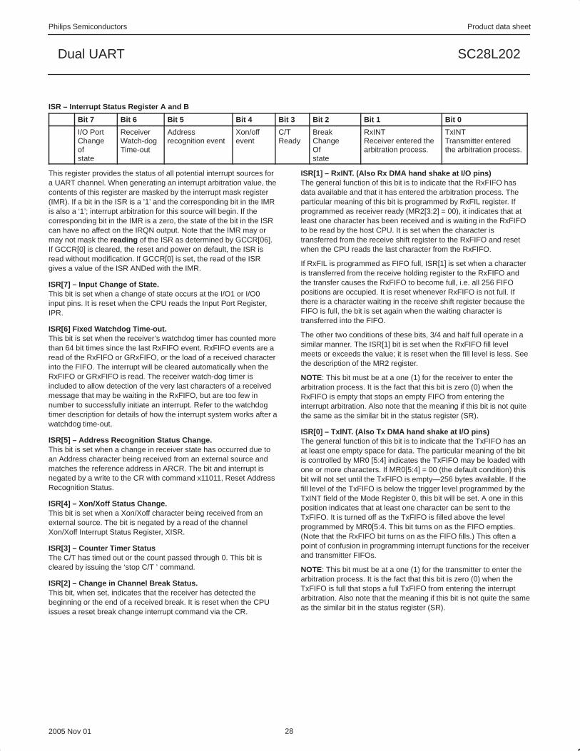
Philips Semiconductors Product data sheet
SC28L202Dual UART
2005 Nov 01 28
ISR – Interrupt Status Register A and B
Bit 7 Bit 6 Bit 5 Bit 4 Bit 3 Bit 2 Bit 1 Bit 0
I/O PortChangeofstate
ReceiverWatch-dogTime-out
Addressrecognition event
Xon/offevent
C/TReady
BreakChangeOfstate
RxINTReceiver entered thearbitration process.
TxINTTransmitter enteredthe arbitration process.
This register provides the status of all potential interrupt sources fora UART channel. When generating an interrupt arbitration value, thecontents of this register are masked by the interrupt mask register(IMR). If a bit in the ISR is a ’1’ and the corresponding bit in the IMRis also a ‘1’; interrupt arbitration for this source will begin. If thecorresponding bit in the IMR is a zero, the state of the bit in the ISRcan have no affect on the IRQN output. Note that the IMR may ormay not mask the reading of the ISR as determined by GCCR[06].If GCCR[0] is cleared, the reset and power on default, the ISR isread without modification. If GCCR[0] is set, the read of the ISRgives a value of the ISR ANDed with the IMR.
ISR[7] – Input Change of State.This bit is set when a change of state occurs at the I/O1 or I/O0input pins. It is reset when the CPU reads the Input Port Register,IPR.
ISR[6] Fixed Watchdog Time-out.This bit is set when the receiver’s watchdog timer has counted morethan 64 bit times since the last RxFIFO event. RxFIFO events are aread of the RxFIFO or GRxFIFO, or the load of a received characterinto the FIFO. The interrupt will be cleared automatically when theRxFIFO or GRxFIFO is read. The receiver watch-dog timer isincluded to allow detection of the very last characters of a receivedmessage that may be waiting in the RxFIFO, but are too few innumber to successfully initiate an interrupt. Refer to the watchdogtimer description for details of how the interrupt system works after awatchdog time-out.
ISR[5] – Address Recognition Status Change.This bit is set when a change in receiver state has occurred due toan Address character being received from an external source andmatches the reference address in ARCR. The bit and interrupt isnegated by a write to the CR with command x11011, Reset AddressRecognition Status.
ISR[4] – Xon/Xoff Status Change.This bit is set when a Xon/Xoff character being received from anexternal source. The bit is negated by a read of the channelXon/Xoff Interrupt Status Register, XISR.
ISR[3] – Counter Timer StatusThe C/T has timed out or the count passed through 0. This bit iscleared by issuing the ‘stop C/T ’ command.
ISR[2] – Change in Channel Break Status.This bit, when set, indicates that the receiver has detected thebeginning or the end of a received break. It is reset when the CPUissues a reset break change interrupt command via the CR.
ISR[1] – RxINT. (Also Rx DMA hand shake at I/O pins)The general function of this bit is to indicate that the RxFIFO hasdata available and that it has entered the arbitration process. Theparticular meaning of this bit is programmed by RxFIL register. Ifprogrammed as receiver ready (MR2[3:2] = 00), it indicates that atleast one character has been received and is waiting in the RxFIFOto be read by the host CPU. It is set when the character istransferred from the receive shift register to the RxFIFO and resetwhen the CPU reads the last character from the RxFIFO.
If RxFIL is programmed as FIFO full, ISR[1] is set when a characteris transferred from the receive holding register to the RxFIFO andthe transfer causes the RxFIFO to become full, i.e. all 256 FIFOpositions are occupied. It is reset whenever RxFIFO is not full. Ifthere is a character waiting in the receive shift register because theFIFO is full, the bit is set again when the waiting character istransferred into the FIFO.
The other two conditions of these bits, 3/4 and half full operate in asimilar manner. The ISR[1] bit is set when the RxFIFO fill levelmeets or exceeds the value; it is reset when the fill level is less. Seethe description of the MR2 register.
NOTE: This bit must be at a one (1) for the receiver to enter thearbitration process. It is the fact that this bit is zero (0) when theRxFIFO is empty that stops an empty FIFO from entering theinterrupt arbitration. Also note that the meaning if this bit is not quitethe same as the similar bit in the status register (SR).
ISR[0] – TxINT. (Also Tx DMA hand shake at I/O pins)The general function of this bit is to indicate that the TxFIFO has anat least one empty space for data. The particular meaning of the bitis controlled by MR0 [5:4] indicates the TxFIFO may be loaded withone or more characters. If MR0[5:4] = 00 (the default condition) thisbit will not set until the TxFIFO is empty—256 bytes available. If thefill level of the TxFIFO is below the trigger level programmed by theTxINT field of the Mode Register 0, this bit will be set. A one in thisposition indicates that at least one character can be sent to theTxFIFO. It is turned off as the TxFIFO is filled above the levelprogrammed by MR0[5:4. This bit turns on as the FIFO empties.(Note that the RxFIFO bit turns on as the FIFO fills.) This often apoint of confusion in programming interrupt functions for the receiverand transmitter FIFOs.
NOTE: This bit must be at a one (1) for the transmitter to enter thearbitration process. It is the fact that this bit is zero (0) when theTxFIFO is full that stops a full TxFIFO from entering the interruptarbitration. Also note that the meaning if this bit is not quite the sameas the similar bit in the status register (SR).

Philips Semiconductors Product data sheet
SC28L202Dual UART
2005 Nov 01 29
IMR – Interrupt Mask Register A and B
Bit 7 Bit 6 Bit 5 Bit 4 Bit 3 Bit 2 Bit 1 Bit 0
I/O Port Change of state Rx Watch-dogTime-out
Addressrecognition event
Xon/offevent
C/TReady
Break ChangeOf State
RxRDYinterrupt
TxRDYinterrupt
The programming of this register selects which bits in the ISR causean interrupt output. If a bit in the ISR is a ’1’ and the correspondingbit in the IMR is a ’1’, the interrupt source is presented to the internalinterrupt arbitration circuits, eventually resulting in the IRQN outputbeing asserted (low). If the corresponding bit in the IMR is a zero,the state of the bit in the ISR has no affect on the IRQN output.
IMR[7] COS enableAllows a change of state in the inputs equipped with input changedetectors to cause an interrupt.
IMR[6] Fixed Watchdog EnableControls the generation of an interrupt watchdog timer event. If set,a count of 64 idle bit times in the receiver will begin interruptarbitration.
IMR[5] Address recognition enableEnables the generation of an interrupt in response to changes in theAddress Recognition circuitry of the Special Mode (multi-drop orwake-up mode).
IMR[4] Xon/Xoff EnableEnables the generation of an interrupt in response to recognition ofan in-band flow control character.
IMR[3] Counter/Timer EnableEnable the C/T interrupt when the C/T reaches 0 count.[2] Enablesthe generation of an interrupt when a Break condition has beendetected by the channel receiver.
IMR[1] Receiver (Rx) EnableEnables the generation of an interrupt when servicing for theRxFIFO is desired.
IMR[0] Transmitter (Tx) EnableEnables the generation of an interrupt when servicing for theTxFIFO is desired.
RxFIFO – Receiver FIFO, A and B
Bit[10] Bit[9] Bit[8] Bits [7:0]These bits are sent to the status register This the data byte sent to the data bus on RxFIFO read
BreakReceived Status
FramingError Status
ParityError Status
8 data bitsMSBs =0 for 7,6,5 bit data
The FIFO for the receiver is 11 bits wide and 256 ‘words’ deep. Thestatus of each byte received is stored with that byte and is movedalong with the byte as the characters are read from the FIFO. Theupper three bits are presented in the STATUS register and theychange in the status register each time a data byte is read from theFIFO. Therefor the status register should be read BEFORE the byteis read from the RxFIFO if one wishes to ascertain the quality of thebyte.
The foregoing applies to the ‘character error’ mode of statusreporting. See MR1[5] and ‘RxFIFO Status’ descriptions for ‘blockerror’ status reporting. Briefly, ‘Block Error’ gives the accumulatederror of all bytes received by the RxFIFO since the last ‘Reset Error’command was issued. (CR = 0x04)
TxFIFO – Transmitter FIFO, A and B
Bits 7:08 data bits. MSBs are ignored to 0 for 7, 6, 5 bit data
The FIFO for the transmitter is 8 bits wide by 256 bytes deep. For character lengths less than 8 bits the upper bits will be ignored by thetransmitter state machine and thus are effectively discarded.
RxFIL – Receiver FIFO Interrupt Level, A and B
Bits 7:0Any one of 256 FIFO fill positions
The position in the Rx FIFO that causes the receiver will enter the interrupt arbitration process. This register is used to offset the effect of thearbitration threshold. It use may yield moderate improvements in the interrupt service. It will also ‘equalize’ interrupt latency and allow for largeraggregate block transfers between fast and slow channels. Writing to this register removes the interrupt control established in MR0 and MR1.
RxFL – Receiver FIFO Fill Level Register
Bits 7:0Channel byte count code ** (1) = implied ‘1’
00000001 = 100000010 = 2to11111111 = 255**(1)00000000 = 256 if RxRDY status bit is set.
The number of bytes filled in the receiver FIFO

Philips Semiconductors Product data sheet
SC28L202Dual UART
2005 Nov 01 30
TxFIL – Transmitter FIFO Interrupt Level A and B
Bits 7:0
Any one of 256 FIFO empty positions
The position in the Tx FIFO that caused the transmitter will enter the interrupt arbitration process. This register is used to offset the effect of thearbitration threshold. It use may yield moderate improvements in the interrupt service. It will also ‘equalize’ interrupt latency and allow for largeraggregate block transfers between fast and slow channels. Writing to this register removes the interrupt control established in MR0 and MR1.
TxEL – Transmitter FIFO Empty Level Register
Bits 7:0
Channel byte count code ** (1) = implied ‘1’
00000001 = 100000010 = 2to11111111 = 255**(1)00000000 = 256 if TxRDY status bit is set.
The number of empty bytes in the Transmitter FIFO.
Registers for Character RecognitionPlease not that, although the names of the registers imply a particular function, there is not any hardware function directly attached to them.They are just three characters that may be used for any function requiring recognition or simple character stripping.
It is only when other internal logic is enabled that the reception of a recognized character will trigger particular chip functions and/or interrupts.
XonCR – Xon/Xoff Character Register A and B
Bits 7:0
8 Bits of the Xon Character Recognition (Resets to 0x11)
An 8-bit character register that contains the compare value for a Xon character.
XoffCR – Xoff Character Register A and B
Bits 7:0
8 Bits of the Xoff Character Recognition (Resets to 0x13)
An 8-bit character register that contains the compare value for a Xoff character.
ARCR – Address Recognition Character Register A and B
Bits 7:0
8 Bits of the Multi-Drop Address Character Recognition (Resets to 0x00)
An 8 bit character register that contains the compare value for the wake-up address character.

Philips Semiconductors Product data sheet
SC28L202Dual UART
2005 Nov 01 31
XISR – Xon–Xoff Interrupt Status Register A and B (Reading this register clears XISR(7:4))
Bits 7:6 Bits 5:4 Bits 3:2 Bits 1:0
Received X Character Status Automatic X Character transmissionstatus
TxD flow status TxD character status
00 = none01 = Xoff received10 = Xon received11 = both received
00 = none01 = Xon transmitted10 = Xoff transmitted11 = Both transmitted
00 = normal transmission01 = TxD halt pending10 = re-enabled11 = flow halted
00 = normal TxD data01 = Idle wait for FIFOdata10 = Xoff in pending11 = Xon in pending
XISR[7:6] Received X Character Status.This field can be read to determine if the receiver has encountered aXon or Xoff character in the incoming data stream. These bits aremaintained until a read of the XISR. The field is updated by Xcharacter reception regardless of the state of MR3(7) and MR3(3:2)or IMR(4). The field can therefore be used as a character detectorfor the bit patterns stored in the Xon and Xoff Character Registers.
XISR[5:4] Automatic transmission Status.This field indicates the last flow control character sent in the AutoReceiver flow control mode. If Auto Receiver mode has not beenenabled, this field will always read b’00. It will likewise reset to b’00 ifMR0(3) is reset. If the Auto Receiver mode is exited while this fieldreads b’10, it is the user’s responsibility to transmit a Xon, whenappropriate.
XISR[3:2] TxD Condition of the automatic flow control status.This field tracks the transmitter’s flow status as follows:
• 00 – normal transmission. Transmitter is not affected by Xon orXoff.
• 01 – TxD halt pending. After the current character finishes thetransmitter will stop. The status will then change to b’11.
• 10 – re–enabled. The transmitter had been halted and has beenrestarted. It is sending (or is prepared to send) data characters.
After a read of the XISR, it will return to ‘normal’ status.
• 11 – The transmitter is stopped due to an Xoff character beingreceived from its associated receiver. The transmitter is ‘flowcontrolled’.
XISR[1:0] TxD X character Status.This field allows determination of the type of character beingtransmitted. It will always be b’00 if none of the automatic Xcharacter controls of MR3[3:2] is enabled.
• 01 – The channel is waiting for a data character to transfer fromthe TxFIFO. This condition will only occur for a bit time after a Xonor Xoff character transmission unless the TxFIFO is empty.
• 10 – A command to send an Xoff character is pending.
• 11 – A command to send an Xon character is pending.
Conditions b’10 and b’11 will not exist for more than a charactertime.
WCXER Watch Dog, Character, Address and X Enable Register – A and B
Bit 7 Bit 6 Bit 5 Bit 4 BIT 3 BIT 2 BIT 1 BIT 0
Watch dog * Address recognition Xon recognition Xoff Recognition
1 = disable Wd0 = no action
1 = enableWd0 = no action
1 = disable Ar0 = no action
1 = enable Ar0 = no action
1 = disableXon0 = no action
1 = enableXon0 = no action
1 = disableXoff0 = no action
1 = enableXoff0 = no action
This register enables the UART’s Character Recognition, AddressRecognition and Receiver watchdog timer. If both enable anddisable are active a disable results. This register is used to enablethe general–purpose character recognition feature WITHOUT
causing any Xon/Xoff or wakeup mode activities to occur. Therecognition event is reported in the ISR register.
* This bit control is duplicated at MR0[7].

Philips Semiconductors Product data sheet
SC28L202Dual UART
2005 Nov 01 32
Programmable Counters, Timers and Baud Rate generatorsPBRGPU – Programmable BRG Timer Reload Registers, Upper 0 and 1
Bits 7:08 MSBs of the BRG Timer divisor.
This is the upper byte of the 16–bit value used by the BRG timer in generating a baud rate clock
PBRGPL – Programmable BRG Timer Reload Registers, Lower 0 and 1
Bits 7:08 LSB of the BRG Timer divisor.
This is the lower byte of the 16–bit value used by the BRG timer in generating a baud rate clock.
CTCS 0 and 1 – Counter Timer clock source
NOTE: Writing to this register removes the control established in the counter/timer portion of the ACR in the default register map
Bit 7:6 Bit 5:4 Bit 3:0Reserved Mode control Clock selection
00 – Selects Counter Mode. Generates a timing edge
01 – Selects Timer Mode. Generates a square wave
10 – Reserved
11 – Selects Timer Pulse Mode. Generates periodic pulses twice the frequency as in Timer Mode. Pulse width is one cycle of the clock as it is delivered to the C/T. (i.e. after any prescale)
0000 External I/O2 A (for CT 0), I/O7 A (for CT 1)0001 External I/O2 A/16 (for CT 0), I/O7 A/16 (for CT 1)0010 Sclk0011 Sclk / 20100 Sclk / 160101 Sclk / 320110 Sclk / 640111 Sclk / 128TxC1X ATxC1X B1010, 1011 Reserved1100 Rx Character Count (Ch A) Clock is RxFIFO A load pulse1101 Rx Character Count (Ch B) Clock is RxFIFO B load pulse1110, 1111 Reserved
CTVU – Counter Timer Value Registers, Upper 0 and 1
Bits 7:08 MSBs of the Counter timer preset value
Reading this register gives the value of the upper 8 bits of the counter timer.
CTVL – Counter timer Value Registers, Lower 0 and 1
Bits 7:08 LSB of the Counter timer preset value
Reading this register gives the value of the upper 8 bits of thecounter timer.
NOTE: The counter timer should be stopped before reading. Usuallythe clock of the counter timer is not synchronized with the read ofthe C/T. It is therefore possible to capture changing data during theread. Depending on the clock speed with respect to the read cycle
this could be made worse or completely eliminated. If the Stopcounter command is issued and following that the C/T is read therewill be no uncertainty go its value. If it is necessary to read the C/T‘on the fly’ then reading it twice and comparing the values willcorrect the problem. The double read will not be effective if thecounter timer clock is faster than a read cycle.
PBRGCS – Programmable BRG Clock Source
Bit 7 Bit 6:4 Bit 3 Bit 2:0PBRG 1, Register control PBRG 1, Clock selection PBRG 0, Register control PBRG 0, Clock selection
0 = Resets PBRG 1 andholds it stopped
1 = Allows PBRG 1 to run.
000 = Sclk001 = Sclk / 2010 = Sclk/ 16011 = Sclk / 32100 = Sclk / 64101 = Sclk / 128110 = I/O4 A111 = Reserved
0 = Resets PBRG 0 andholds it stopped.
1 = Allows PBRG 0 to run.
000 = Sclk001 = Sclk / 2010 = Sclk / 16011 = Sclk / 32100 = Sclk / 64101 = Sclk / 128110 = I/O3 A111 = Reserved
Start/Stop control and clock select register for the two BRGcounters. The clock selection is for the input to the counters. It isthat clock divided by the number represented by the PBRGPU andPBRGPL the will be used as the 16x clock for the receivers andtransmitters. When the BRG timer Clock is selected for the
receiver(s) or transmitter(s) the receivers and transmitters willconsider it as a 16x clock and further device it by 16. In other wordsthe receivers and transmitters will always be in the 16x ode ofoperation when the internal BRG timer is selected for their clock.

Philips Semiconductors Product data sheet
SC28L202Dual UART
2005 Nov 01 33
CTPU Counter Timer Preset Upper 0 and 1
CTPU Bit 7 BIT 6 BIT 5 BIT 4 BIT 3 BIT 2 BIT 1 BIT 0The lower eight (8) bits for the 16 bit counter timer preset register
CTPL Counter –Timer Preset Low 0 and 1
CTPL Bit 7 BIT 6 BIT 5 BIT 4 BIT 3 BIT 2 BIT 1 BIT 0The Upper eight (8) bits for the 16 bit counter timer preset register
The CTPU and CTPL hold the eight MSBs and eight LSBs,respectively, of the value to be used by the counter/timer in eitherthe counter or timer modes of operation. The minimum value thatmay be loaded into the CTPU/CTPL registers is H‘0000’. Note thatthese registers are write–only and cannot be read by the CPU.
In the timer mode, the C/T generates a square wave whose period istwice the value (in C/T clock periods) of the CTPU and CTPL. Thewaveform so generated is often used for a data clock. The formulafor calculating the divisor n to load to the CTPU and CTPL for aparticular 1X data clock is shown below.
NOTE: The 2 in the denominator is for the Square wave generation.For the Pulse mode change the 2 to a 1.
n C/T clock input frequency
(2 16 (Baud rate desired))
(If the pulse mode is selected, then ‘2’ in the divisor should be ‘1’.This doubles the C/T output speeds for any given input clock.)
Often this division will result in a non–integer number, 26.3 forexample. One can only program integer numbers in a digital divider.Therefore, 26 would be chosen. This gives a baud rate error of0.3/26.3, which is 1.14% and well within the ability asynchronousmode of operation.
If the value in CTPU and CTPL is changed, the current half–periodwill not be affected, but subsequent half periods will be. The C/T willnot be running until it receives an initial ‘Start Counter’ commandfrom the command register (or a read at address A6–A0 = 0001110in the lower 16 position address space) . After this, while in timermode, the C/T will run continuously. Receipt of a start countercommand causes the counter to terminate the current timing cycleand to begin a new cycle using the values in CTPU and CTPL.
The counter ready status bit (ISR [3]) is set once each cycle of thesquare wave. The bit is reset by a stop counter command from thecommand register (or a read with A6–A0 = 0x0F in the lower 16position address space). The command however, does not stop theC/T. the generated square wave is output on I/O3 if it is programmedto be the C/T output. In the counter mode, the value C/T loaded intoCTPU and CTPL by the CPU is counted down to 0. Counting beginsupon receipt of a start counter command. Upon reaching terminalcount H‘0000’, the counter ready interrupt bit (ISR [3]) is set. Thecounter continues counting past the terminal count until stopped by
the CPU. If I/O3 is programmed to be the output of the C/T, theoutput remains high until terminal count is reached; at which time itgoes low. The output returns to the High State and ISR [3] is clearedwhen the counter is stopped by a stop counter command. The CPUmay change the values of CTPU and CTPL at any time, but the newcount becomes effective only on the next start counter commands. Ifnew values have not been loaded, the previous count values arepreserved and used for the next count cycle
In the counter mode, the current value of the upper and lower 8 bitsof the counter (CTPU, CTPL) may be read by the CPU. It isrecommended that the counter be stopped when reading to preventpotential problems that may occur if a carry from the lower 8 bits tothe upper 8 bits occurs between the times that both halves of thecounter are read. However, note that a subsequent start countercommand will cause the counter to begin a new count cycle usingthe values in CTPU and CTPL. When the C/T clock divided by 16 isselected, the maximum divisor becomes 1,048,575.The CTS, RTS, CTS Enable Tx signalsCTS (Clear To Send) is usually meant to be a signal to thetransmitter meaning that it may transmit data to the receiver. TheCTS input is on pin I/O0 A for Tx A and on I/O1 A for Tx B. The CTSsignal is active low; thus; it is called CTSN A for Tx A and CTSN Bfor Tx B. RTS is usually meant to be a signal from the receiverindicating that the receiver is ready to receive data. It is also activelow and is, thus, called RTSN A for Rx A and RTSN B for Rx B.RTSN A is on pin I/O0 B and RTSN B is on I/O1 B. A receiver’sRTSN output will usually be connected to the CTS input of theassociated transmitter. Therefore, one could say that RTS and CTSare different ends of the same wire!
MR2 (4) is the bit that allows the transmitter to be controlled by theCTS pin (I/O0 A or I/O1 A). When this bit is set to one AND the CTSinput is driven high, the transmitter will stop sending data at the endof the present character being serialized. It is usually the RTS outputof the receiver that will be connected to the transmitter’s CTS input.The receiver will set RTS high when the receiver FIFO is full ANDthe start bit of the ninth character is sensed. Transmission thenstops with nine valid characters in the receiver. When MR2 (4) is setto one, CTSN must be at zero for the transmitter to operate. If MR2(4) is set to zero, the I/O pin will have no effect on the operation ofthe transmitter. MR1 (7) is the bit that allows the receiver to controlI/O0 B. When the receiver controls I/O0 B (or I/O1 B), the meaningof that pin will be the RTSN function.
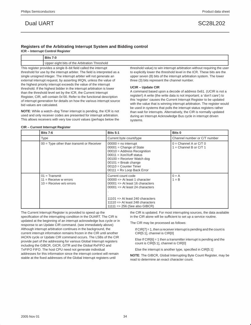
Philips Semiconductors Product data sheet
SC28L202Dual UART
2005 Nov 01 34
Registers of the Arbitrating Interrupt System and Bidding controlICR – Interrupt Control Register
Bits 7:0
Upper eight bits of the Arbitration Threshold
This register provides a single 8–bit field called the interruptthreshold for use by the interrupt arbiter. The field is interpreted as asingle unsigned integer. The interrupt arbiter will not generate anexternal interrupt request, by asserting IRQN, unless the value ofthe highest priority interrupt exceeds the value of the interruptthreshold. If the highest bidder in the interrupt arbitration is lowerthan the threshold level set by the ICR, the Current InterruptRegister, CIR, will contain 0x’00. Refer to the functional descriptionof interrupt generation for details on how the various interrupt sourcebid values are calculated.
NOTE: While a watch–dog Timer interrupt is pending, the ICR is notused and only receiver codes are presented for interrupt arbitration.This allows receivers with very low count values (perhaps below the
threshold value) to win interrupt arbitration without requiring the userto explicitly lower the threshold level in the ICR. These bits are theupper seven (8) bits of the interrupt arbitration system. The lowerthree (3) bits represent the channel number.
UCIR – Update CIRA command based upon a decode of address 0x61. (UCIR is not aregister!) A write (the write data is not important; a ‘don’t care’) tothis ’register’ causes the Current Interrupt Register to be updatedwith the value that is winning interrupt arbitration. The register wouldbe used in systems that polls the interrupt status registers ratherthan wait for interrupts. Alternatively, the CIR is normally updatedduring an Interrupt Acknowledge Bus cycle in interrupt drivensystems.
CIR – Current Interrupt Register
Bits 7:6 Bits 5:1 Bits 0
Type Current byte count/type Channel number or C/T number
00 = Type other than transmit or Receiver 00000 = no interrupt00001 = Change of State00010 = Address Recognition00011 = Xon/Xoff status00100 = Receiver Watch dog00101 = Break change00110 = Counter Timer00111 = Rx Loop Back Error
0 = Channel A or C/T 01 = Channel B or C/T 1
01 = Transmit11 = Receive w errors10 = Receive w/o errors
Current count code00000 => At least 1 character00001 => At least 16 characters00001 => At least 24 characters..11101 => At least 240 characters11110 => At least 248 characters11111 => 256 (See also GIBCR)
0 = A1 = B
The Current Interrupt Register is provided to speed up thespecification of the interrupting condition in the DUART. The CIR isupdated at the beginning of an interrupt acknowledge bus cycle or inresponse to an Update CIR command. (see immediately above)Although interrupt arbitration continues in the background, thecurrent interrupt information remains frozen in the CIR until anotherIACKN cycle or Update CIR command occurs. The LSBs of the CIRprovide part of the addressing for various Global Interrupt registersincluding the GIBCR, GICR, GITR and the Global RxFIFO andTxFIFO FIFO. The host CPU need not generate individualaddresses for this information since the interrupt context will remainstable at the fixed addresses of the Global Interrupt registers until
the CIR is updated. For most interrupting sources, the data availablein the CIR alone will be sufficient to set up a service routine.
The CIR may be processed as follows:
If CIR[7] = 1, then a receiver interrupt is pending and the count isCIR[5:1], channel is CIR[0]
Else If CIR[6] = 1 then a transmitter interrupt is pending and thecount is CIR[5:1], channel is CIR[0]
Else the interrupt is another type, specified in CIR[5:1]
NOTE: The GIBCR, Global Interrupting Byte Count Register, may beread to determine an exact character count.

Philips Semiconductors Product data sheet
SC28L202Dual UART
2005 Nov 01 35
IVR – Interrupt Vector Register
Bits 7:0
8 data bits of the Interrupt Vector (IVR)
The IVR contains the byte that will be placed on the data bus during an IACKN cycle when the GCCR bits (2:1) are set to binary ‘01’. This is theunmodified form of the interrupt vector.
Modification of the IVR
Bits 7:3 Bits 2:1 Bit 0
Always contains bits (7:3) of the IVR Will be replaced with current interrupt type if IVC field of GCCR = 3
Replaced with interrupting channel number if IVC field of GCCR > 1
The table above indicates how the IVR may be modified by the interrupting source. The modification of the IVR as it is presented to the data busduring an IACK cycle is controlled by the setting of the bits (2:1) in the GCCR (Global Chip Configuration Register).
GICR – Global Interrupting Channel Register
Bits 7:1 Bit 0
Reserved Channel code
0 = a1 = b
A register associated with the interrupting channel as defined in the CIR. It contains the channel number for the interrupting channel.
GIBCR – Global Interrupting Byte Count Register
Bits 7:0
Channel byte count code
00000001 = 100000010 = 2.11111111 = 25500000000 = 256
A register associated with the interrupting channel as defined in theCIR. Its numerical value equals TxEL or RxFL at the time IACKN or‘Update CIR’ command was issued . The true number of bytes
ready for transfer to the transmitter or transfer from the receiver. It isundefined for other types of interrupts
GITR – Global Interrupting Type Register
Bit 7:6 Bit 5 Bit 4:3 Bit 2:0
Receiver Interrupt Transmitter Interrupt Reserved Other types
0x = not receiver10 = with receive errors11 = w/o receive errors
0 = not transmitter1 = transmitter interrupt
read 0x00 000 = not ‘other’ type001 = Change of State010 = Address Recognition Event011 = Xon/Xoff status
100 = Rx Watchdog101 = Break Change110 = Counter Timer111 = Rx Loop Back Error
A register associated with the interrupting channel as defined in the CIR. It contains the type of interrupt code for all interrupts.
GRxFIFO – Global RxFIFO Register
Bits 7:0
8 data bits of RxFIFO. MSBs set to 0 for 7, 6, 5 bit data
The RxFIFO of the channel indicated in the CIR channel field. Undefined when the CIR interrupt context is not a receiver interrupt. GlobalTxFIFO Register
GTxFIFO – Global TxFIFO Register
Bits 7:0
8 data bits of TxFIFO. MSBs not used for 7, 6, 5 bit data
The TxFIFO of the channel indicated in the CIR channel field. Undefined when the CIR interrupt context is not a transmitter interrupt. Writing tothe GTxFIFO when the current interrupt is not a transmitter event may result in the characters being transmitted on a different channel thanintended.

Philips Semiconductors Product data sheet
SC28L202Dual UART
2005 Nov 01 36
BCRBRK – Bidding Control Register – Break Change, A and B
Bits 7:0
MSBs of break change interrupt bid
This register provides the 8 MSBs of the Interrupt Arbitration number for a break change interrupt.
BCRCOS – Bidding Control Register – Change of State, A and B
Bits 7:0
MSBs of Change of state detectors (COS) interrupt bid
This register provides the 8 MSBs of the Interrupt Arbitration number for a Change of State, COS, interrupt.
BCRx – Bidding Control Register – Xon/Xoff, A and B
Bits 7:0
MSBs of an Xon/Xoff interrupt bid
This register provides the 8 MSBs of the Interrupt Arbitration number for a Xon/Xoff interrupt.
BCRA – Bidding Control Register – Address, A and B
Bits 7:0
MSBs of an address recognition event interrupt bid
This register provides the 8 MSBs of the Interrupt Arbitration number for an address recognition event interrupt.
BCR C/T – Bidding Control Register –C/T, 0 and 1
Bits 7:0
MSBs of a counter/timer event interrupt bid
This register provides the 8 MSBs of the Interrupt Arbitration number for a counter/timer event interrupt.
BCRLBE – Bidding Control Register – Received Loop Back Error
Bits 7:0
MSBs of a received loop back error event interrupt bid
This register provides the 8 MSBs of the Interrupt Arbitration number for the received loop back error interrupt.Registers of the I/O ports
IPCRL – Input Port Change Register Lower Nibble, A and B (n = A for A, n = B for B)
Bit 7 Bit 6 Bit 7 Bit 6 Bit 3 Bit 2 Bit 1 Bit 0
∆I/O3 nchange
∆I/O2 nchange
∆I/O1 nchange
∆I/O0 nchange
I/O3 n state I/O2 n state I/O1 n state I/O0 nstate
0 = no change1 = change
0 = no change1 = change
0 = no change1 = change
0 = no change1 = change
Reads the actual logic level at the pin.1 = high level; 0 = low level
This register may be read to determine the current logical level of the I/O pins and examine the output of the change detectors assigned to eachpin. If the change detection is not enabled or if the pin is configured as an output, the associated change field will read b’0.
IPCRU – Input Port Change Register Upper Nibble, A and B (n = A for A, n = B for B)
Bit 7 Bit 6 Bit 7 Bit 6 Bit 3 Bit 2 Bit 1 Bit 0
∆I/O7 n change ∆I/O6 n change ∆I/O5 n change ∆I/O4 n change I/O7 n state I/0n6 state I/O5 n state I/O4 n state
0 = no change1 = change
0 = no change1 = change
0 = no change1 = change
0 = no change1 = change
Reads the actual logic level at the pin.1 = high level; 0 = low level
This register may be read to determine the current logical level of the I/O pins and examine the output of the change detectors assigned to eachpin. If the change detection is not enabled or if the pin is configured as an output, the associated change field will read b’0.
IPR – Input Port Register, A and B (n = A for A, n = B for B)
Bits 7:0
Logical levels of I/O(7:0)n
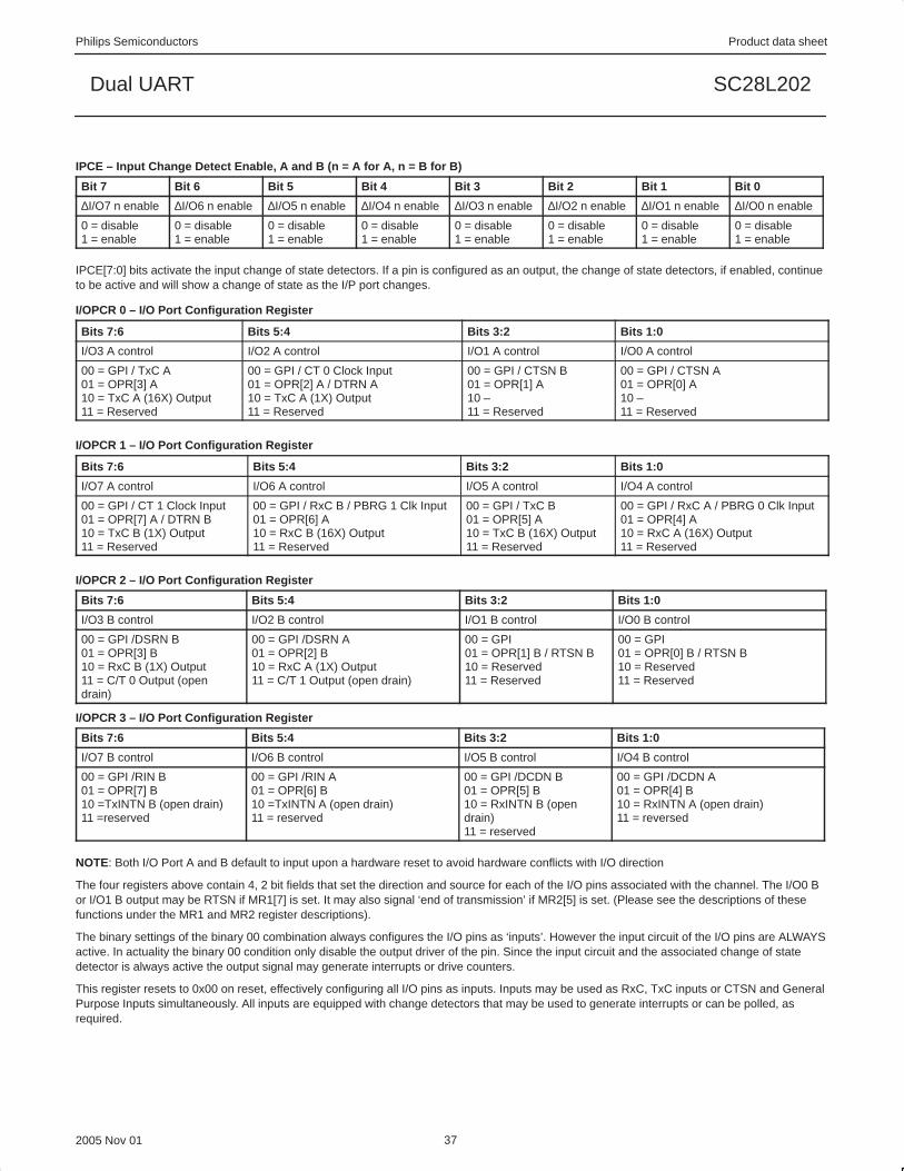
Philips Semiconductors Product data sheet
SC28L202Dual UART
2005 Nov 01 37
IPCE – Input Change Detect Enable, A and B (n = A for A, n = B for B)
Bit 7 Bit 6 Bit 5 Bit 4 Bit 3 Bit 2 Bit 1 Bit 0
∆I/O7 n enable ∆I/O6 n enable ∆I/O5 n enable ∆I/O4 n enable ∆I/O3 n enable ∆I/O2 n enable ∆I/O1 n enable ∆I/O0 n enable
0 = disable1 = enable
0 = disable1 = enable
0 = disable1 = enable
0 = disable1 = enable
0 = disable1 = enable
0 = disable1 = enable
0 = disable1 = enable
0 = disable1 = enable
IPCE[7:0] bits activate the input change of state detectors. If a pin is configured as an output, the change of state detectors, if enabled, continueto be active and will show a change of state as the I/P port changes.
I/OPCR 0 – I/O Port Configuration Register
Bits 7:6 Bits 5:4 Bits 3:2 Bits 1:0
I/O3 A control I/O2 A control I/O1 A control I/O0 A control
00 = GPI / TxC A01 = OPR[3] A10 = TxC A (16X) Output11 = Reserved
00 = GPI / CT 0 Clock Input01 = OPR[2] A / DTRN A10 = TxC A (1X) Output11 = Reserved
00 = GPI / CTSN B01 = OPR[1] A10 –11 = Reserved
00 = GPI / CTSN A01 = OPR[0] A10 –11 = Reserved
I/OPCR 1 – I/O Port Configuration Register
Bits 7:6 Bits 5:4 Bits 3:2 Bits 1:0
I/O7 A control I/O6 A control I/O5 A control I/O4 A control
00 = GPI / CT 1 Clock Input01 = OPR[7] A / DTRN B10 = TxC B (1X) Output11 = Reserved
00 = GPI / RxC B / PBRG 1 Clk Input01 = OPR[6] A10 = RxC B (16X) Output11 = Reserved
00 = GPI / TxC B01 = OPR[5] A10 = TxC B (16X) Output11 = Reserved
00 = GPI / RxC A / PBRG 0 Clk Input01 = OPR[4] A10 = RxC A (16X) Output11 = Reserved
I/OPCR 2 – I/O Port Configuration Register
Bits 7:6 Bits 5:4 Bits 3:2 Bits 1:0
I/O3 B control I/O2 B control I/O1 B control I/O0 B control
00 = GPI /DSRN B01 = OPR[3] B10 = RxC B (1X) Output11 = C/T 0 Output (opendrain)
00 = GPI /DSRN A01 = OPR[2] B10 = RxC A (1X) Output11 = C/T 1 Output (open drain)
00 = GPI01 = OPR[1] B / RTSN B10 = Reserved11 = Reserved
00 = GPI01 = OPR[0] B / RTSN B10 = Reserved11 = Reserved
I/OPCR 3 – I/O Port Configuration Register
Bits 7:6 Bits 5:4 Bits 3:2 Bits 1:0
I/O7 B control I/O6 B control I/O5 B control I/O4 B control
00 = GPI /RIN B01 = OPR[7] B10 =TxINTN B (open drain)11 =reserved
00 = GPI /RIN A01 = OPR[6] B10 =TxINTN A (open drain)11 = reserved
00 = GPI /DCDN B01 = OPR[5] B10 = RxINTN B (opendrain)11 = reserved
00 = GPI /DCDN A01 = OPR[4] B10 = RxINTN A (open drain)11 = reversed
NOTE: Both I/O Port A and B default to input upon a hardware reset to avoid hardware conflicts with I/O direction
The four registers above contain 4, 2 bit fields that set the direction and source for each of the I/O pins associated with the channel. The I/O0 Bor I/O1 B output may be RTSN if MR1[7] is set. It may also signal ‘end of transmission’ if MR2[5] is set. (Please see the descriptions of thesefunctions under the MR1 and MR2 register descriptions).
The binary settings of the binary 00 combination always configures the I/O pins as ‘inputs’. However the input circuit of the I/O pins are ALWAYSactive. In actuality the binary 00 condition only disable the output driver of the pin. Since the input circuit and the associated change of statedetector is always active the output signal may generate interrupts or drive counters.
This register resets to 0x00 on reset, effectively configuring all I/O pins as inputs. Inputs may be used as RxC, TxC inputs or CTSN and GeneralPurpose Inputs simultaneously. All inputs are equipped with change detectors that may be used to generate interrupts or can be polled, asrequired.
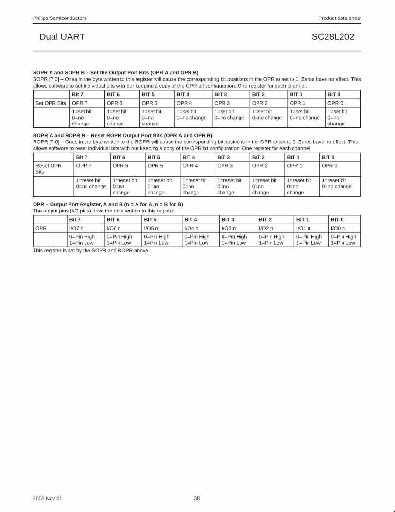
Philips Semiconductors Product data sheet
SC28L202Dual UART
2005 Nov 01 38
SOPR A and SOPR B – Set the Output Port Bits (OPR A and OPR B)SOPR [7:0] – Ones in the byte written to this register will cause the corresponding bit positions in the OPR to set to 1. Zeros have no effect. Thisallows software to set individual bits with our keeping a copy of the OPR bit configuration. One register for each channel.
Bit 7 BIT 6 BIT 5 BIT 4 BIT 3 BIT 2 BIT 1 BIT 0
Set OPR Bits OPR 7 OPR 6 OPR 5 OPR 4 OPR 3 OPR 2 OPR 1 OPR 0
1=set bit0=nochange
1=set bit0=nochange
1=set bit0=nochange
1=set bit0=no change
1=set bit0=no change
1=set bit0=no change
1=set bit0=no change
1=set bit0=nochange
ROPR A and ROPR B – Reset ROPR Output Port Bits (OPR A and OPR B)ROPR [7:0] – Ones in the byte written to the ROPR will cause the corresponding bit positions in the OPR to set to 0. Zeros have no effect. Thisallows software to reset individual bits with our keeping a copy of the OPR bit configuration. One register for each channel
Bit 7 BIT 6 BIT 5 BIT 4 BIT 3 BIT 2 BIT 1 BIT 0
Reset OPRBits
OPR 7 OPR 6 OPR 5 OPR 4 OPR 3 OPR 2 OPR 1 OPR 0
1=reset bit0=no change
1=reset bit0=nochange
1=reset bit0=nochange
1=reset bit0=nochange
1=reset bit0=nochange
1=reset bit0=nochange
1=reset bit0=nochange
1=reset bit0=no change
OPR – Output Port Register, A and B (n = A for A, n = B for B)The output pins (I/O pins) drive the data written to this register.
Bit 7 BIT 6 BIT 5 BIT 4 BIT 3 BIT 2 BIT 1 BIT 0
OPR I/O7 n I/O6 n I/O5 n I/O4 n I/O3 n I/O2 n I/O1 n I/O0 n
0=Pin High1=Pin Low
0=Pin High1=Pin Low
0=Pin High1=Pin Low
0=Pin High1=Pin Low
0=Pin High1=Pin Low
0=Pin High1=Pin Low
0=Pin High1=Pin Low
0=Pin High1=Pin Low
This register is set by the SOPR and ROPR above.

Philips Semiconductors Product data sheet
SC28L202Dual UART
2005 Nov 01 39
THE REGISTERS FOR COMPATIBILITY WITH PREVIOUS DUARTSThe purpose of including previous functionality is to allow users tocall communications code that may be used in former systems.When the registers in this lower 16–position address space is usedit will revoke programming done in the upper address space wherethe addresses are duplicated. If functions have been called fromupper address space that DO NOT exist in the lower address spacethey will remain active. It is therefore recommended that the ‘Reset
to C92’ command be issued before calling code written for olderdevices. This is just recommended. If one wishes to enhanceprevious code by using Xon/Xoff, for example, there is no restrictionagainst it. These registers provide the original functionality ofprevious Philips DUARTs: SCN2681, SCN68681, SCC2691,SCC68692, SC26C92 and SC28L92.
Table 7. SC28L92 Register Addressing READ (RDN = 0) WRITE (WRN = 0)Address READ (RDN = 0) WRITE (WRN = 0)
0 0 0 0 Mode Register A (MR0 A, MR1 A, MR2 A) Mode Register A (MR0 A, MR1 A, MR2 A)
0 0 0 1 Status Register A (SR A) Clock Select Register A (CSR A )
0 0 1 0 Reserved Command Register A (CR A)
0 0 1 1 Rx Holding Register A (RxFIFO A) Tx Holding Register A (TxFIFO A)
0 1 0 0 Input Port Change Register (IPCR) Aux. Control Register (ACR)
0 1 0 1 Interrupt Status Register (ISR) Interrupt Mask Register (IMR)
0 1 1 0 Counter/Timer Upper (CTPU) C/T Upper Preset Register (CTPU)
0 1 1 1 Counter/Timer Lower (CTPL) C/T Lower Preset Register (CTPL)
1 0 0 0 Mode Register B (MR0 B, MR1 B, MR2 B) Mode Register B (MR0 B, MR1 B, MR2 B)
1 0 0 1 Status Register B (SR B) Clock Select Register B (CSR B )
1 0 1 0 Reserved Command Register B (CR B)
1 0 1 1 Rx Holding Register B (RxFIFO B) Tx Holding Register B (TxFIFO B)
1 1 0 0 IVR or general purpose register IVR or general purpose register
1 1 0 1 Input Port (IPR) I/O(6:0) A Output Port Confide. Register (OPCR) I/O(7:2) B
1 1 1 0 Start Counter Command (C/T 0) Set Output Port Bits Command (SOPR) I/O(7:0) B
1 1 1 1 Stop Counter Command (C/T 0) Reset output Port Bits Command (ROPR) I/O(7:0) B
NOTE: The three MR Registers are accessed via the MR Pointer and Commands 0x1n and 0xBn (where n = represents receiver andtransmitter enable bits)
The following registers are unique for each Channel
Mode Register MRn A MRn B R/W
Status Register SR A SR B R only
ClockSelect
CSR A CSR B W only
CommandRegister
CR A CR B W only
ReceiverFIFO
RxFIFO A RxFIFO B R only
TransmitterFIFO
TxFIFO A TxFIFO B W only
These registers support functions for both Channels
Input Port Change Register IPCR R
Auxiliary Control Register ACR W
Interrupt Status Register ISR R
Interrupt Mask Register IMR W
Counter Timer Upper Value CTPU R
Counter Timer Lower Value CTPL R
Counter Timer Preset Upper CTPU W
Counter Timer Preset Lower CTPL W
Input Port Register IPR R
Output Configuration Register OPCR W
Set Output Port Bits W
Reset Output Port Bits W

Philips Semiconductors Product data sheet
SC28L202Dual UART
2005 Nov 01 40
Table 8. Baud Rate Generator CharacteristicsCrystal or Clock = 14.7456 MHz
NORMAL RATE(BAUD)
ACTUAL 16XCLOCK (kHz)
ERROR (%) NORMAL RATE(BAUD)
ACTUAL 16XCLOCK (kHz)
ERROR (%)
50 0.8 0 2400 38.4 0
75 1.2 0 4800 76.8 0
110 1.759 –0.069 7200 115.2 0
134.5 2.153 0.059 9600 153.6 0
150 2.4 0 19.2K 307.2 0
200 3.2 0 38.4K 614.4 0
300 4.8 0 14.4K 230.4 0
600 9.6 0 28.8K 460.8 0
1050 16.756 –0.260 31.25 500.0 1.6
1200 19.2 0 57.6k 921.6 0
1800 28.8 0 115.2K 1843.2 0
2000 32.056 0.175 230.4K 3686.4 0
NOTE: Duty cycle of 16X clock is 50% ± 1%
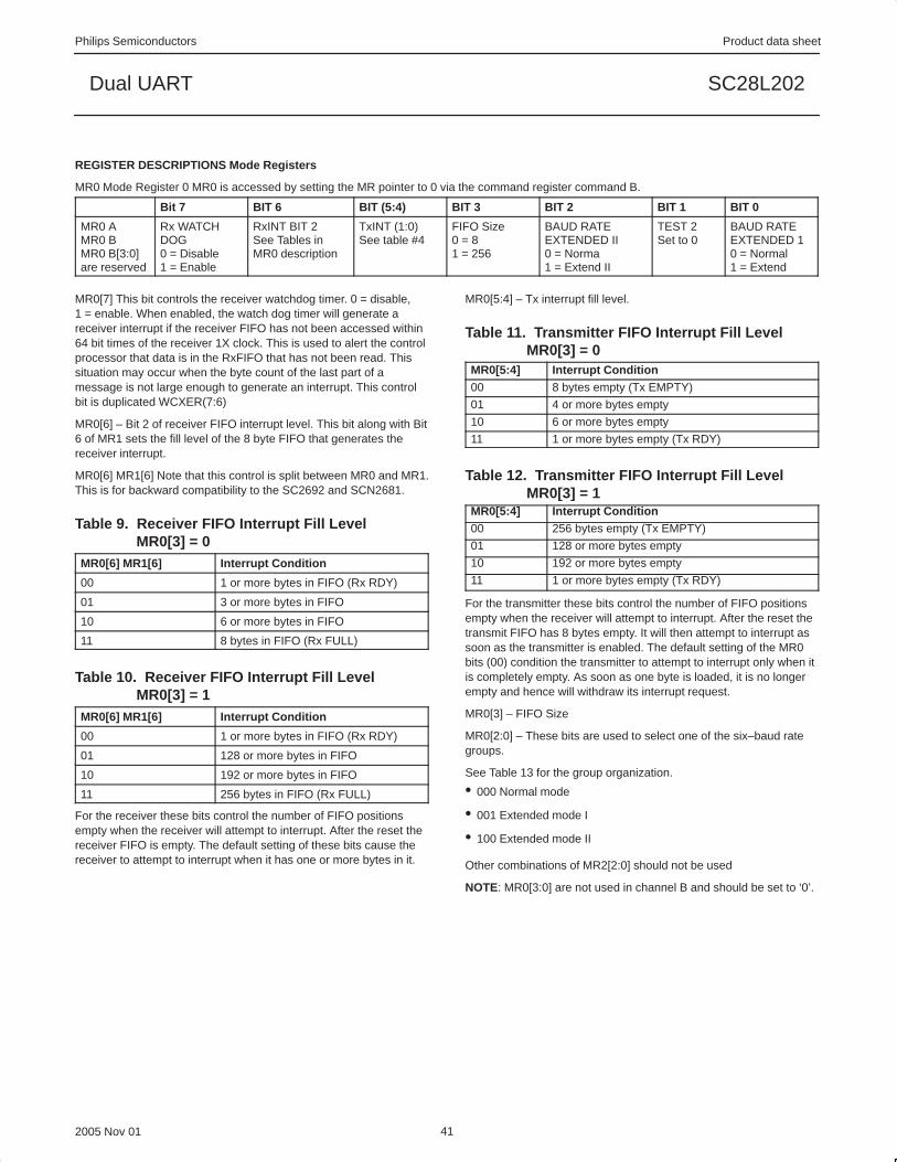
Philips Semiconductors Product data sheet
SC28L202Dual UART
2005 Nov 01 41
REGISTER DESCRIPTIONS Mode Registers
MR0 Mode Register 0 MR0 is accessed by setting the MR pointer to 0 via the command register command B.
Bit 7 BIT 6 BIT (5:4) BIT 3 BIT 2 BIT 1 BIT 0
MR0 AMR0 BMR0 B[3:0]are reserved
Rx WATCHDOG0 = Disable1 = Enable
RxINT BIT 2See Tables inMR0 description
TxINT (1:0)See table #4
FIFO Size0 = 81 = 256
BAUD RATEEXTENDED II0 = Norma1 = Extend II
TEST 2Set to 0
BAUD RATEEXTENDED 10 = Normal1 = Extend
MR0[7] This bit controls the receiver watchdog timer. 0 = disable,1 = enable. When enabled, the watch dog timer will generate areceiver interrupt if the receiver FIFO has not been accessed within64 bit times of the receiver 1X clock. This is used to alert the controlprocessor that data is in the RxFIFO that has not been read. Thissituation may occur when the byte count of the last part of amessage is not large enough to generate an interrupt. This controlbit is duplicated WCXER(7:6)
MR0[6] – Bit 2 of receiver FIFO interrupt level. This bit along with Bit6 of MR1 sets the fill level of the 8 byte FIFO that generates thereceiver interrupt.
MR0[6] MR1[6] Note that this control is split between MR0 and MR1.This is for backward compatibility to the SC2692 and SCN2681.
Table 9. Receiver FIFO Interrupt Fill LevelMR0[3] = 0
MR0[6] MR1[6] Interrupt Condition
00 1 or more bytes in FIFO (Rx RDY)
01 3 or more bytes in FIFO
10 6 or more bytes in FIFO
11 8 bytes in FIFO (Rx FULL)
Table 10. Receiver FIFO Interrupt Fill LevelMR0[3] = 1
MR0[6] MR1[6] Interrupt Condition
00 1 or more bytes in FIFO (Rx RDY)
01 128 or more bytes in FIFO
10 192 or more bytes in FIFO
11 256 bytes in FIFO (Rx FULL)
For the receiver these bits control the number of FIFO positionsempty when the receiver will attempt to interrupt. After the reset thereceiver FIFO is empty. The default setting of these bits cause thereceiver to attempt to interrupt when it has one or more bytes in it.
MR0[5:4] – Tx interrupt fill level.
Table 11. Transmitter FIFO Interrupt Fill LevelMR0[3] = 0
MR0[5:4] Interrupt Condition00 8 bytes empty (Tx EMPTY)
01 4 or more bytes empty
10 6 or more bytes empty
11 1 or more bytes empty (Tx RDY)
Table 12. Transmitter FIFO Interrupt Fill LevelMR0[3] = 1
MR0[5:4] Interrupt Condition00 256 bytes empty (Tx EMPTY)
01 128 or more bytes empty
10 192 or more bytes empty
11 1 or more bytes empty (Tx RDY)
For the transmitter these bits control the number of FIFO positionsempty when the receiver will attempt to interrupt. After the reset thetransmit FIFO has 8 bytes empty. It will then attempt to interrupt assoon as the transmitter is enabled. The default setting of the MR0bits (00) condition the transmitter to attempt to interrupt only when itis completely empty. As soon as one byte is loaded, it is no longerempty and hence will withdraw its interrupt request.
MR0[3] – FIFO Size
MR0[2:0] – These bits are used to select one of the six–baud rategroups.
See Table 13 for the group organization.
• 000 Normal mode
• 001 Extended mode I
• 100 Extended mode II
Other combinations of MR2[2:0] should not be used
NOTE: MR0[3:0] are not used in channel B and should be set to ‘0’.

Philips Semiconductors Product data sheet
SC28L202Dual UART
2005 Nov 01 42
MR1 Mode Register 1
Bit 7 BIT 6 BIT 5 Bit (4:3) BIT 2 Bits (1:0)
MR1 AMR1 B
RxCONTROLSRTS
RxINTBIT 1
ERRORMODE
PARITY MODE PARITYTYPE
BITS PERCHARACTER
0 = No1 = Yes
0 = RxRDY1 = FFULL
0 = Char1 = Block
00 = With Parity01 = Force Parity10 = No Parity11 = Multi–drop Mode
0 = Even1 = Odd
00 = 501 = 610 = 711 = 8
NOTE: * In block error mode the block error conditions must be cleared by using the error reset command (command 0x40) or a receiver reset.
MR1 A is accessed when the Channel A MR pointer points to MR1.The pointer is set to MR1 by RESET or by a ‘set pointer’ commandapplied via CR command 1. After reading or writing MR1 A, thepointer will point to MR2 A.
MR1 A[7] – Channel A Receiver Request–to–Send Control (FlowControl)This bit controls the deactivation of the RTSN A output (I/O0 B) bythe receiver. This output is normally asserted by setting OPR[0]Band negated by resetting OPR[0]B.
MR1 A[7] = 1 causes RTSN A to be negated (I/O0 B is driven to a ‘1’[VCC]) upon receipt of a valid start bit if the Channel A FIFO is full.This is the beginning of the reception of the ninth byte. If the FIFO isnot read before the start of the tenth byte, an overrun condition willoccur and the tenth byte will be lost. However, the bit in OPR[0] isnot reset and RTSN A will be asserted again when an empty FIFOposition is available. This feature can be used for flow control toprevent overrun in the receiver by using the RTSN A output signal tocontrol the CTSN input of the transmitting device.
MR1[6] – Receiver interrupt control bit 1. See description underMR0[6].
MR1 A[5] – Channel A Error Mode SelectThis bit select the operating mode of the three FIFOed status bits(FE, PE, received break) for Channel A. In the ‘character’ mode,status is provided on a character–by–character basis; the statusapplies only to the character at the top of the FIFO. In the ‘block’
mode, the status provided in the SR for these bits is theaccumulation (logical–OR) of the status for all characters coming tothe top of the FIFO since the last ‘reset error’ command for ChannelA was issued.
MR1 A[4:3| – Channel A Parity Mode SelectIf ‘with parity’ or ‘force parity’ is selected a parity bit is added to thetransmitted character and the receiver performs a parity check onincoming data
MR1 A[4:3] = 11 selects Channel A to operate in the specialmulti–drop mode described in the Operation section.
MR1 A[2] – Channel A Parity Type SelectSelects the parity type (odd or even) if the ‘‘with parity’ mode isprogrammed by MR1 A[4:3], and the polarity of the forced parity bit ifthe ‘force parity’ mode is programmed; no effect if ‘no parity’ isprogrammed. In the special multi–drop mode it selects the polarity ofthe A/D bit.
MR1 A[1:0] – Channel A Bits Per Character SelectThis field selects the number of data bits per character to betransmitted and received. The character length does not include thestart, parity, and stop bits.
MR2 A is accessed when the Channel A MR pointer points to MR2,which occurs after any access to MR1 A. Accesses to MR2 A do notchange the pointer.
MR2 Mode Register 2
Bit 7 BIT 6 BIT 5 BIT 4 BIT 3 BIT 2 BIT 1 BIT 0
MR2 AMR2 B
CHANNEL MODE Tx CONTROLS RTS CTSENABLE Tx
STOP BIT LENGTHNOTE: Add 0.5 to binary codes 0 – 7 for 5 bit character lengths.
00 = Normal01 = Auto–Echo10 = Local loop11 = Remote loop
0 = No1 = Yes
0 = No1 = Yes
0 = 0.563 4 = 0.813 8 = 1.563 C = 1.8131 = 0.625 5 = 0.875 9 = 1.625 D = 1.8752 = 0.688 6 = 0.938 A = 1.688 E = 1.9383 = 0.750 7 = 1.000 B = 1.750 F = 2.000
NOTE: *Add 0.5 to values shown for 0 – 7 if channel is programmed for 5 bits/char.
See description in the previous MR2 description

Philips Semiconductors Product data sheet
SC28L202Dual UART
2005 Nov 01 43
SR Status Register
Bit 7 BIT 6 BIT 5 BIT 4 BIT 3 BIT 2 BIT 1 BIT 0
SR ASR B
RECEIVEDBREAK*
FRAMINGERROR*
PARITYERROR*
OVERRUNERROR
TxEMT TxRDY FFULL RxRDY
0 = No1 = Yes
0 = No1 = Yes
0 = No1 = Yes
0 = No1 = Yes
0 = No1 = Yes
0 = No1 = Yes
0 = No1 = Yes
0 = No1 = Yes
NOTE: *These status bits are appended to the corresponding data character in the receive FIFO. A read of the status provides these bits(7:5) from the top of the FIFO together with bits (4:0). These bits are cleared by a ‘reset error status’ command. In character mode they arediscarded when the corresponding data character is read from the FIFO. In block error mode, the error–reset command (command 4x orreceiver reset) must used to clear block error conditions
SR A[7] – Received BreakChannel A Received Break. This bit indicates that an all zerocharacter of the programmed length has been received without astop bit. Only a single FIFO position is occupied when a break isreceived: further entries to the FIFO are inhibited until the RxD A linereturns to the marking state for at least one–half a bit time twosuccessive edges of the internal or external 1X clock. This willusually require a high time of one X1 clock period or 3 X1 edgessince the clock of the controller is not synchronous to the X1 clock.
When this bit is set, the Channel A ‘change in break’ bit in the ISR(ISR[2]) is set. ISR[2] is also set when the end of the breakcondition, as defined above, is detected.
The break detect circuitry can detect breaks that originate in themiddle of a received character. However, if a break begins in themiddle of a character, it must persist until at least the end of the nextcharacter time in order for it to be detected.This bit is reset by command 4 (0100) written to the commandregister or by receiver reset.
SR A[6] – Channel A Framing ErrorThis bit, when set, indicates that a stop bit was not detected whenthe corresponding data character in the FIFO was received. Thestop bit check is made in the middle of the first stop bit position.
SR A[5] – Channel A Parity ErrorThis bit is set when the ‘with parity’ or ‘force parity’ mode isprogrammed and the corresponding character in the FIFO wasreceived with incorrect parity.
In the special multi–drop mode the parity error bit stores the receiveA/D (Address/Data) bit.
SR A[4] – Channel A Overrun ErrorThis bit, when set, indicates that one or more characters in thereceived data stream have been lost. It is set upon receipt of a newcharacter when the FIFO is full and a character is already in thereceive shift register waiting for an empty FIFO position. When thisoccurs, the character in the receive shift register (and its breakdetect, parity error and framing error status, if any) is lost.
This bit is cleared by a ‘reset error status’ command.
SR A[3] – Channel A Transmitter Empty (TxEMT A)This bit will be set when the transmitter under runs, i.e., both theTxEMT and TxRDY bits are set. This bit and TxRDY are set whenthe transmitter is first enabled and at any time it is re–enabled aftereither (a) reset, or (b) the transmitter has assumed the disabledstate. It is always set after transmission of the last stop bit of acharacter if no character is in the THR awaiting transmission.
It is reset when the THR is loaded by the CPU, a pendingtransmitter disable is executed, the transmitter is reset, or thetransmitter is disabled while in the under run condition.
SR A[2] – Channel A Transmitter Ready (TxRDY A)This bit, when set, indicates that the transmit FIFO is not full andready to be loaded with another character. This bit is cleared whenthe transmit FIFO is loaded by the CPU and there are (after thisload) no more empty locations in the FIFO. It is set when acharacter is transferred to the transmit shift register. TxRDY A isreset when the transmitter is disabled and is set when thetransmitter is first enabled. Characters loaded to the TxFIFO whilethis bit is 0 will be lost. This bit has different meaning from ISR[0].
SR A[1] – Channel A FIFO Full (FFULL A)This bit is set when a character is transferred from the receive shiftregister to the receive FIFO and the transfer causes the FIFO tobecome full, i.e., all eight FIFO positions are occupied. It is resetwhen the CPU reads the receive FIFO. If a character is waiting inthe receive shift register because the FIFO is full, FFULL A will notbe reset when the CPU reads the receive FIFO. This bit hasdifferent meaning from ISR1 when MR1 6 is programmed to a ‘1’.
SR A[0] – Channel A Receiver Ready (RxRDY A)This bit indicates that a character has been received and is waitingin the FIFO to be read by the CPU. It is set when the character istransferred from the receive shift register to the FIFO and resetwhen the CPU reads the receive FIFO, only if (after this read) thereare no more characters in the FIFO.
SR B – Channel B Status RegisterThe bit definitions for this register are identical to the bit definitionsfor SR A, except that all status applies to the Channel B receiverand transmitter and the corresponding inputs and outputs.

Philips Semiconductors Product data sheet
SC28L202Dual UART
2005 Nov 01 44
CSR A – Channel A Clock Select Register CSR A [7:4] – Channel A Receiver Clock SelectThis field selects the baud rate clock for the Channel A receiver. The field definition is shown in Table 13.
CSR Clock Select Register
Bit 7 BIT 6 BIT 5 BIT 4 BIT 3 BIT 2 BIT 1 BIT 0
CSR A & CSR B RECEIVER CLOCK SELECT TRANSMITTER CLOCK SELECT
See Text and Table 13 See Text and Table 13
Table 13. Baud Rate (Base on a 14.7456 MHz crystal clock)MR0[0] = 0 (Normal Mode) MR0[0] = 1 (Extended Mode I) MR0[2] = 1 (Extended Mode II)
CSR A [7:4] ACR[7] = 0 ACR[7] = 1 ACR[7] = 0 ACR[7] = 1 ACR[7] = 0 ACR[7] = 1
0000 50 75 300 450 4,800 7,200
0001 110 110 110 110 880 880
0010 134.5 134.5 134.5 134.5 1,076 1,076
0011 200 150 1200 900 19.2K 14.4K
0100 300 300 1800 1800 28.8K 28.8K
0101 600 600 3600 3600 57.6K 57.6K
0110 1,200 1,200 7200 7,200 115.2K 115.2K
0111 1,050 2,000 1,050 2,000 1,050 2,000
1000 2,400 2,400 14.4K 14.4K 57.6K 57.6K
1001 4,800 4,800 28.8K 28.8K 4,800 4,800
1010 7,200 1,800 7,200 1,800 57.6K 14.4K
1011 9,600 9,600 57.6K 57.6K 9,600 9,600
1100 38.4K 19.2K 230.4K 115.2K 38.4K 19.2K
1101 Timer Timer Timer Timer Timer Timer
1110 I/O4 A–16X I/O4 A–16X I/O4 A–16X I/O4 A–16X I/O4 A–16X I/O4 A–16X
1111 I/O4 A–1X I/O4 A–1X I/O4 A–1X I/O4 A–1X I/O4 A–1X I/O4 A–1X
NOTE: The receiver clock is always a 16X clock except for CSR A [7:4] = 1111.
CSR A [3:0] – Channel A EXTERNAL Transmitter Clock SelectThis field selects the baud rate clock for the Channel A transmitter.The field definition is as shown in Table 13, except as follows:
CSR A [3:0] ACR[7] = 0 ACR[7] = 1
1110 I/O3 A–16X I/O3 A–16X
1111 I/O3 A–1X I/O3 A–1X
The transmitter clock is always a 16X clock except forCSR[3:0] = 1111.
CSR B [7:4] – Channel B Receiver Clock SelectThis field selects the baud rate clock for the Channel B receiver. Thefield definition is as shown in Table 13, except as follows:
CSR B [7:4] ACR[7] = 0 ACR[7] = 1
1110 I/O6 A–16X I/O6 A–16X
111 I/O6 A–1X I/O6 A–1X
The receiver clock is always a 16X clock except forCSR B[7:4] = 1111.
CSR B [3:0] – Channel B Transmitter Clock SelectThis field selects the baud rate clock for the Channel B transmitter.The field definition is as shown in Table 13, except as follows:
CSR B [3:0] ACR[7] = 0 ACR[7] = 1
1110 I/O5 A–16X I/O5 A–16X
1111 I/O5 A–1X I/O5 A–1X
The transmitter clock is always a 16X clock except forCSR B[3:0] = 1111.
Rx FIFO Register. For characters shorter than 8 bits the unused bits are set to zero
Bit 7 BIT 6 BIT 5 BIT 4 BIT 3 BIT 2 BIT 1 BIT 0
Bits of the received data characters.
Tx FIFO register. For characters shorter than 8 bits the unused bits are set to zero
Bit 7 BIT 6 BIT 5 BIT 4 BIT 3 BIT 2 BIT 1 BIT 0
Bits of the data characters to be transmitted

Philips Semiconductors Product data sheet
SC28L202Dual UART
2005 Nov 01 45
CR A and B Command RegisterCR, one for each channel, controls the channel commands and enables/disables the receiver and transmitter. Commands may be to the upperand lower four bits in the same bus cycle. If both enable and disable bits are set to 1 in the lower four bits a disable will result.
CR Command Register
Bit 7 BIT 6 BIT 5 BIT 4 BIT 3 BIT 2 BIT 1 BIT 0
CR A &CR B MISCELLANEOUS COMMANDS Disable Tx Enable Tx Disable Rx Enable Rx
See Text of Channel Command Register 1 = Yes0 = No
1 = Yes0 = No
1 = Yes0 = No
1 = Yes0 = No
NOTE: Access to the miscellaneous commands should be separated by 3 X1 clock edges. A disabled transmitter cannot be loaded.
COMMAND REGISTER TABLE A and BCommands 0xE, 0xF (marked with *) are global and exist only in channel A’s register space.
Channel Command Code Channel Command Channel Command Code Channel Command
CR[7:4] Description CR[7:4] Description
0000 NOP 1000 Assert RTSN (I/O0 B or I/O1 B)
0001 Set MR pointer to 1 1001 Negate RTSN (I/O0 B or I/O1 B)
0010 Reset Receiver 1010 Set C/T Receiver time–out mode on
0011 Reset Transmitter 1011 Set MR pointer to 0
0100 Reset Error Status 1100 Set C/T Receiver time–out mode off
0101 Reset Break Change Interrupt 1101 Block Error Status on RxFIFO load
0110 Begin Transmit Break 1110 • Power Down Mode On
0111 End Transmit Break 1111 • Disable Power Down Mode
• 0000 No command.
• 0001 set MR pointer to 1
• 0010 Reset receiver. Immediately resets the receiver as ifhardware reset had been applied. The receiver is reset and theFIFO pointer is reset to the first location effectively discarding allunread characters in the FIFO.
• 0011 Reset transmitter. Immediately resets the transmitter as if ahardware reset had been applied. The transmitter is reset and theFIFO pointer is reset to the first location effectively discarding alluntransmitted characters in the FIFO.
• 0100 Reset error status. Clears the received break, parity error,framing error, and overrun error bits in the status register(SR[7:4]). I
It is used in either character or block mode. In block mode it wouldnormally be used after the block is read.
• 0101 Reset break change interrupt. Causes the break detectchange bit in the interrupt status register (ISR[2]) to be cleared tozero.
• 0110 Start break. Forces the TxD output low (spacing). If thetransmitter is empty, the start of the break condition will bedelayed up to two bit times. If the transmitter is active and theTxFIFO is empty then the break begins when transmission of thecurrent character is completed. If there are characters in theTxFIFO, the start of break is delayed until all characters presentlyin the TxFIFO and any subsequent characters loaded have beentransmitted. (Tx Idle must be true before break begins).
The transmitter must be enabled to start a break.
• 0111 Stop break. The TxD line will go high (marking) within two bittimes. TxD will remain high for one bit time before the nextcharacter is transmitted.
• 1000 Assert RTSN. Causes the RTSN output to be asserted (low).
• 1001 Negate RTSN. Causes the RTSN output to be negated(high).
NOTE: The two commands above actually reset and set,respectively, the I/O0 B or I/O1 B pin associated WITH theOPR register.
• 1010 Set C/T Receiver time out mode on. The receiver in thischannel will restart the C/T as reach receive character istransferred from the shift register to the RxFIFO. The C/T isplaced in the Counter Mode, the Start/Stop Counter commandsare disabled, the counter is stopped and the Counter Ready bit,ISR(3), is reset.
• 1011 Set MR Pointer to 0
• 1100 Set C/T Receiver time out mode off
• 1101 Block error status accumulation on FIFO entry. Allows the‘received break’, ‘framing error’ and ‘parity error’ bits to be set asthe received character is loaded to the RxFIFO. (normally thesebits are set on reading of the data from the RxFIFO) Setting thismode can give information about error data up to 256 bytes earlierthan the normal mode. However it clouds the ability to knowprecisely which byte(s) are in error.
• 1110 Power Down Mode On
• 1111 Disable Power Down Mode

Philips Semiconductors Product data sheet
SC28L202Dual UART
2005 Nov 01 46
IPCR Input Port Configuration Register
Bit 7 BIT 6 BIT 5 BIT 4 BIT 3 BIT 2 BIT 1 BIT 0
IPCR DeltaI/O 3A
DeltaI/O 2A
DeltaI/O 1A
DeltaI/O 0A
I/O 3A I/O 2A I/O 1A I/O 0A
0 = no change1 = change
0 = no change1 = change
0 = no change1 = change
0 = no change1 = change
0 = low1 = High
0 = low1 = High
0 = low1 = High
0 = low1 = High
IPCR [7:4] I/03A, I/O2 A, I/O1 A, I/O0 A Change–of–StateThese bits are set when a change–of–state, as defined in the inputport section of this data sheet, occurs at the respective input pins.They are cleared when the IPCR is read by the CPU. A read ofthe IPCR also clears ISR [7], the input change bit in the interruptstatus register. The setting of these bits can be programmed togenerate an interrupt to the CPU.
IPCR [3:0] I/O3 A, I/O2 A, I/O1 A, I/O0 A logical level of I/O pin.These bits provide the current state of the respective inputs. Theinformation is unlatched and reflects the state of the input pins at thetime the IPCR is read.
ACR Auxiliary Control Register
Bit 7 BIT 6 BIT 5 BIT 4 BIT 3 BIT 2 BIT 1 BIT 0
ACRBRG SETSelect
Counter Timer Modeandclock source select
DeltaI/O3 A interruptenable
DeltaI/O2 A interruptenable
DeltaI/O1 A interruptenable
DeltaI/O0 A interruptenable
0 = set 11 = set 2
See Table 14 0 = off1 = enabled
0 = off1 = enabled
0 = off1 = enabled
0 = off1 = enabled
ACR[7] – Baud Rate Generator Set SelectThis bit selects one of two sets of baud rates to be generated by theBRG and it effects both channels. (see Table 13).
ACR[6:4] – Counter/Timer Mode And Clock Source SelectThis field selects the operating mode of the counter/timer and itsclock source as shown in Table 14.
ACR[3:0] – I/O3 A, I/O2 A, I/O1 A, I/O0 A Change-of-StateInterrupt EnableThis field selects which bits of the input port change register (IPCR)cause the input change bit in the interrupt status register (ISR [7]) tobe set. If a bit is in the ‘on’ state the setting of the corresponding bitin the IPCR will also result in the setting of ISR[7], which results inthe generation of an interrupt output if IMR[7] = 1. If a bit is in the‘off’ state, the setting of that bit in the IPCR has no effect on ISR[7].
Table 14. ACR 6:4 Field DefinitionACR(6:4) MODE CLOCK SOURCE
000 Counter External (I/02A)
001 Counter TxC A – 1X clock of Channel Atransmitter
010 Counter TxC B – 1X clock of Channel Btransmitter
011 Counter (X1/Sclk) clock divided by 16
100 Timer External (I/O 2A)
101 Timer External (I/O2 A) divided by 16
110 Timer Crystal or external clock (X1/Sclk)
111 Timer (X1/Sclk) clock divided by 16
NOTE: The timer mode generates a square wave.

Philips Semiconductors Product data sheet
SC28L202Dual UART
2005 Nov 01 47
ISR – Interrupt Status RegisterThis register provides the status of all potential interrupt sources. The contents of this register are masked by the Interrupt Mask Register (IMR).If a bit in the ISR is a ‘1’ and the corresponding bit in the IMR is also a ‘1’ then INTRN output will be asserted (Low). If the corresponding bit inthe IMR is a zero the state of the bit in the ISR has no effect on the INTRN output. Note that the IMR does not mask the reading of the ISR – thetrue status will be provided regardless of the contents of the IMR. The contents of this register are initialized to H‘00’ when the DUART is reset.
ISR Bit 7 BIT 6 BIT 5 BIT 4 BIT 3 BIT 2 BIT 1 BIT 0
INPUTPORTCHANGE
DELTABreak B
RxRDY/FFULL B
TxRDY B CounterReady
DeltaBreak A
RxRDY/FFULL A
TxRDY A
0=not enabled1=enabled
0=not enabled1=enabled
0=not enabled1=enabled
0=not enabled1=enabled
0=not enabled1=enabled
0=not enabled1=enabled
0=not enabled1=enabled
0=not enabled1=enabled
ISR[7] – Input Port Change StatusThis bit is a ‘1’ when a change–of–state has occurred at theI/O(3:0)A or B inputs and that event has been selected to cause aninterrupt by the programming of ACR[3:0]. The bit is cleared whenthe CPU reads the IPCR.
ISR[6] – Channel B Change In BreakThis bit, when set, indicates that the Channel B receiver hasdetected the beginning or the end of a received break. It is resetwhen the CPU issues a Channel B ‘reset break change interrupt’command.
ISR[5] – Rx B InterruptThis bit indicates that the channel B receiver is interruptingaccording to the fill level programmed by the MR0 and MR1registers. This bit has a different meaning than the receiverready/full bit in the status register.
ISR[4] – Tx B InterruptThis bit indicates that the channel B transmitter is interruptingaccording to the interrupt level programmed in the MR0[5:4] bits.This bit has a different meaning than the Tx RDY bit in the statusregister.
ISR[3] – Counter Ready.In the counter mode, this bit is set when the counter reachesterminal count and is reset when the counter is stopped by a stopcounter command.
In the timer mode, this bit is set once each cycle of the generatedsquare wave (every other time that the counter/timer reaches zerocount). The bit is reset by a stop counter command. The command,however, does not stop the counter/timer.
ISR[2] – Channel A Change in BreakThis bit, when set, indicates that the Channel A receiver hasdetected the beginning or the end of a received break. It is resetwhen the CPU issues a Channel A ‘reset break change interrupt’command.
ISR[1] – Rx A InterruptThis bit indicates that the channel A receiver is interruptingaccording to the fill level programmed by the MR0 and MR1registers. This bit has a different meaning than the receiverready/full bit in the status register.
ISR[0] – Tx A InterruptThis bit indicates that the channel A transmitter is interruptingaccording to the interrupt level programmed in the MR0[5:4] bits.This bit has a different meaning than the Tx RDY bit in the statusregister.

Philips Semiconductors Product data sheet
SC28L202Dual UART
2005 Nov 01 48
IMR – Interrupt Mask RegisterThe programming of this register selects which bits in the ISR causes an interrupt output. If a bit in the ISR is a ‘1’ and the corresponding bit inthe IMR is also a ‘1’ the INTRN output will be asserted. If the corresponding bit in the IMR is a zero, the state of the bit in the ISR has no effecton the INTRN output. Note that the IMR does not mask the programmable interrupt outputs I/O3 B–I/O7 B or the reading of the ISR.
IMR Bit 7 BIT 6 BIT 5 BIT 4 BIT 3 BIT 2 BIT 1 BIT 0
INPUT PORTCHANGE
DeltaBreak B
RxRDY/FFULL B
TxRDY B CounterReady
DeltaBreak A
RxRDY/FFULL A
TxRDY A
0=notenabled1=enabled
0=notenabled1=enabled
0=notenabled1=enabled
0=notenabled1=enabled
0=notenabled1=enabled
0=notenabled1=enabled
0=notenabled1=enabled
0=notenabled1=enabled
CTPU Counter Timer Preset Upper (Counter/Timer 0)
CPTU Bit 7 BIT 6 BIT 5 BIT 4 BIT 3 BIT 2 BIT 1 BIT 0
The upper eight (8) bits for the 16 bit counter timer preset register
CTPL Counter –Timer Preset Lower (Counter/Timer 0)
CTPL Bit 7 BIT 6 BIT 5 BIT 4 BIT 3 BIT 2 BIT 1 BIT 0
The lower eight (8) bits for the 16 bit counter timer preset register
CTVU Counter Timer Value Upper (Counter/Timer 0)
CPVL Bit 7 BIT 6 BIT 5 BIT 4 BIT 3 BIT 2 BIT 1 BIT 0
The lower eight (8) bits for the 16 bit counter timer value
CTVL Counter –Timer Value Lower (Counter/Timer 0)
CTVL Bit 7 BIT 6 BIT 5 BIT 4 BIT 3 BIT 2 BIT 1 BIT 0
The lower eight (8) bits for the 16 bit counter timer value register
Only the counter/timer 0 is available in the low order 16–position address map. Issuing the start command loads the C/T with the preset value.The Stop command resets the C/T ready bit in the ISR (Interrupt status Register) and captures the C/T value in the output latches of the C/T. Inthe special time out mode the start and stop commands are ignored. The ‘start command is executed by a read at address 0xE; the stop at 0xF.
IVR Interrupt Vector register in 68K mode and General purpose read write register in the x86 mode
IVR Bit 7 BIT 6 BIT 5 BIT 4 BIT 3 BIT 2 BIT 1 BIT 0
The eight (8) bits of the interrupt vector in the 68K mode.
IPR Input Port Register I/O(6:0) A
IPR Bit 7 BIT 6 BIT 5 BIT 4 BIT 3 BIT 2 BIT 1 BIT 0
Logical levels or the I/O[6:0] A, Bit 7 read as ‘1’

Philips Semiconductors Product data sheet
SC28L202Dual UART
2005 Nov 01 49
OPCR Output Port Configuration Register. Controls [7:2] B
Bit 7 BIT 6 BIT 5 BIT 4 BIT (3:2) BIT (1:0)
I/O7 B I/O6 B I/O5 B I/O4 B I/O3 B I/O2 B
0 = OPR[7]1 = Tx RDY B
0 = OPR[6]1 = Tx RDY A
0 = OPR[5]1 = Rx RDY / FFULL B
0 = OPR[4]1 = Rx RDY / FFULL A
00 = OPR[3]01 = C/T OUTPUT10 = TxC B(1X)11 = RxC B(1X)
00 = OPR[2]01 = TxC A(16X)10 = TxC A(1X)11 = RxC A(1X)
NOTE: I/O0 B and I/O1 B output OPR(0) and OPR(1) respectively.Under program control of MR1 and MR2 the signals RTSN A forI/O0 B and RTSN B for I/O1 B may be assigned.
OPCR[7] – This bit programs the I/O7 B output to provide one of thefollowing:
• 0 The complement of OPR[7].
• 1 The Channel B transmitter interrupt output which is thecomplement of ISR[4]. When in this mode I/O7 acts as an open–drain output. Note that this output is not masked by the contentsof the IMR.
OPCR[6] – This bit programs the I/O6 B output to provide one of thefollowing:
• 0 The complement of OPR[6].
• 1 The Channel A transmitter interrupt output which is thecomplement of ISR[0]. When in this mode I/O6 acts as an open–drain output. Note that this output is not masked by the contentsof the IMR.
OPCR[5] – This bit programs the I/O5 B output to provide one of thefollowing:
• 0 The complement of OPR[5].
• 1 The Channel B receiver interrupt output which is thecomplement of ISR[5]. When in this mode I/O5 acts as anopen–drain output. Note that this output is not masked by thecontents of the IMR.
OPCR[4] – This field programs the I/O4 B output to provide one ofthe following:
• 0 The complement of OPR[4].
• 1 The Channel A receiver interrupt output which is thecomplement of ISR[1]. When in this mode I/O4 acts as an
open–drain output. Note that this output is not masked by thecontents of the IMR.
OPCR[3:2] – This bit programs the I/O3 B output to provide one ofthe following:
• 00 The complement of OPR[3].
• 01 The counter/timer output, in which case I/O3 acts as anopen–drain output. In the timer mode, this output is a square waveat the programmed frequency. In the counter mode, the outputremains high until terminal count is reached, at which time it goeslow. The output returns to the high state when the counter isstopped by a stop counter command. Note that this output is notmasked by the contents of the IMR.
• 10 The 1X clock for the Channel B transmitter that shifts thetransmitted data. If data is not being transmitted, a free running 1Xclock is output.
• 11 The 1X clock for the Channel B receiver that samples thereceived data. If data is not being received, a free running 1Xclock is output.
OPCR[1:0] – This field programs the I/O2 B output to provide one ofthe following:
• 00 The complement of OPR[2].
• 01 The 16X clock for the Channel A transmitter. This is the clockselected by CSR A [3:0], and will be a 1X clock if CSR A [3:0] =1111.
• 10 The 1X clock for the Channel A transmitter that shifts thetransmitted data. If data is not being transmitted, a free running 1Xclock is output.
• 11 The 1X clock for the Channel A receiver that samples thereceived data. If data is not being received, a free running 1Xclock is output.

Philips Semiconductors Product data sheet
SC28L202Dual UART
2005 Nov 01 50
SOPR – Set Bits in the OPROnes in the byte written to this register will cause the corresponding bit positions in the OPR to set to 1. Zeros have no effect. This allowssoftware to set individual bits without keeping a copy of the OPR bit configuration.
Set OPRBits
Bit 7 BIT 6 BIT 5 BIT 4 BIT 3 BIT 2 BIT 1 BIT 0
I/O7 B I/O6 B I/O5 B I/O4 B I/O3 B I/O2 B I/O1 B I/O0 B
1=set bit0=no change
1=set bit0=no change
1=set bit0=no change
1=set bit0=no change
1=set bit0=no change
1=set bit0=no change
1=set bit0=no change
1=set bit0=no change
ROPR – Reset Bits in the OPROnes in the byte written to the ROPR will cause the corresponding bit positions in the OPR to set to 0. Zeros have no effect. This allowssoftware to reset individual bits with our keeping a copy of the OPR bit configuration.
Reset OPRBits
Bit 7 BIT 6 BIT 5 BIT 4 BIT 3 BIT 2 BIT 1 BIT 0
I/O7 B I/O6 B I/O5 B I/O4 B I/O3 B I/O2 B I/O1 B I/O0 B
1=reset bit0=no change
1=reset bit0=no change
1=reset bit0=no change
1=reset bit0=no change
1=reset bit0=no change
1=reset bit0=no change
1=reset bit0=no change
1=reset bit0=no change
OPR Output Port RegisterThe bits in the OPR register are controlled by the use of the SOPR and ROPR commands. The output pins (OP pins) drive the compliment ofthe data stored in this register.
OPR Bit 7 BIT 6 BIT 5 BIT 4 BIT 3 BIT 2 BIT 1 BIT 0
I/O7 B I/O6 B I/O5 B I/O4 B I/O3 B I/O2 B I/O1 B I/O0 B
0=Pin High1=Pin Low
0=Pin High1=Pin Low
0=Pin High1=Pin Low
0=Pin High1=Pin Low
0=Pin High1=Pin Low
0=Pin High1=Pin Low
0=Pin High1=Pin Low
0=Pin High1=Pin Low

Philips Semiconductors Product data sheet
SC28L202Dual UART
2005 Nov 01 51
REGISTER MAPSThe registers of the SC28L202 are loosely partitioned into twogroups: those used in controlling data channels and those used inhandling the actual data flow and status. Below is shown the generalconfiguration of all the register addressed. The ‘Register MapSummary’ shows the configuration of the lower four bits of theaddress that is the same for the individual UARTs . It also showsthe addresses for the several in the address space of UART A andUART B that apply to the total chip configuration. The ‘Register MapDetail’ shows the use of every address in the 8–bit address space.
Any programming using the SC28L202 as it is intended wouldalways use the address space form 0x10 through 0x7F. For the
most part, differences in address between channel A and B differ by0x08.
The first address from 0x00 to 0x0F refer to the legacy code forprevious Philips/Signetics two channel UARTs (DUARTs). Thisfeature is directed to the SC26C92. That part has 89-byte FIFOs,but powers up to look like it has a 3-byte receiver FIFO and a 1-bytetransmitter FIFO. Other control registers structures of legacy partsare compatible back to the SCN2681.
Registers that configure the whole chip are denoted by a ‘ • ’symbol.
REGISTER MAP DETAIL (based on 28L92)NOTE: Addresses 0x00 to 0x0F represent the ‘C92 Register’ map.
A[6:0] READ WRITE
DEFAULT. The first 16 read and write locations are legacy code for other ’92-type UARTs.
000 0000 (0x00) Mode Register (MR0 A, MR1 A, MR2 A) DEFAULT Mode Register (MR0 A, MR1 A, MR2 A) DEFAULT
000 0001 (0x01) Status Register (SR A) Clock Select Register (CSR A) DEFAULT
000 0010 (0x02) Command Register (CR A) DEFAULT
000 0011 (0x03) Receiver FIFO Register (RxFIFO A) Transmitter FIFO Register (TxFIFO A)
000 0100 (0x04) Input Port Change Register (IPCR) DEFAULT • Auxiliary Control Register (ACR) DEFAULT
000 0101 (0x05) • Interrupt Status Register (ISR) DEFAULT • Interrupt Mask Register (IMR) DEFAULT
000 0110 (0x06) Counter Timer Value Register Upper (CTVU 0) Counter Timer Preset Register Upper (CTPU 0)
000 0111 (0x07) Counter Timer Value Register Lower (CTVL 0) Counter Timer Preset Register Lower (CTPL 0)
000 1000 (0x08) Mode Register (MR0 B, MR1 B, MR2 B) DEFAULT Mode Register (MR0 B, MR1 B, MR2 B) DEFAULT
000 1001 (0x09) Status Register (SR B) Clock Select Register (CSR B) DEFAULT
000 1010 (0x0A) Command Register (CR B) DEFAULT
000 1011 (0x0B) Receiver FIFO Register (RxFIFO B) Transmitter FIFO Register (TxFIFO B)
000 1100 (0x0C) • Interrupt Vector Register (IVR) GLOBAL • Interrupt Vector Register (IVR) GLOBAL
000 1101 (0x0D) Input Port Register (IPR) I/O(6:0) A Output Port Configuration Register (OPCR) I/O(7:2)B
000 1110 (0x0E) Start Counter Command DEFAULT C/T 0 Set Output Port Register (SOPR) I/O(7:0)B
000 1111 (0x0F) Stop Counter Command DEFAULT C/T 0 Reset Output Port Register (ROPR) I/O(7:0)B
EXTENSION
001 0000 (0x10) Receiver FIFO Fill Level (RxFL A) Set Output Port Register (SOPR A)
001 0001 (0x11) Transmitter FIFO Empty level (TxEL A) Reset Output Port Register (ROPR A)
001 0010 (0x12) • Enhanced Operation Status (EOS) Command Register Extension (CRx A)
001 0011 (0x13) Input Port Change Register Upper (IPCRU A) I/O Port Configuration Register 0 (I/OPCR 0)
001 0100 (0x14) Input Port Change Register Lower (IPCRL A) I/O Port Configuration Register 1 (I/OPCR 1)
001 0101 (0x15) Input Port Register (IPR A)
001 0110 (0x16) Counter Timer Value Register Upper (CTVU 0) Counter Timer Preset Register Upper (CTPU 0)
001 0111 (0x17) Counter Timer Value Register Lower (CTVL 0) Counter Timer Preset Register Lower (CTPL 0)
001 1000 (0x18) Receiver FIFO Fill Level (RxFL B) Set Output Port Register (SOPR B)
001 1001 (0x19) Transmitter FIFO Empty level (TxEL B) Reset Output Port Register (ROPR B)
001 1010 (0x1A) Command Register Extension (CRx B)
001 1011 (0x1B) Input Port Change Register Upper (IPCRU B) I/O Port Configuration Register 2 (I/OPCR 2)
001 1100 (0x1C) Input Port Change Register Lower (IPCRL B) I/O Port Configuration Register 3 (I/OPCR 3)
001 1101 (0x1D) Input Port Register (IPR B)
001 1110 (0x1E) Counter Timer Value Register Upper (CTVU 1) Counter Timer Preset Register Upper (CTPU 1)
001 1111 (0x1F) Counter Timer Value Register Lower (CTVL 1) Counter Timer Preset Register Lower (CTPL 1)

Philips Semiconductors Product data sheet
SC28L202Dual UART
2005 Nov 01 52
REGISTER MAPNOTE: The register maps for channels A and B (UARTs A and B) contain some control registers that configure the entire chip. These are denoted by a ‘ • ’ symbol
A[6:0] READ WRITE
EXTENSION
010 0000 (0x20) Mode Register 0 (MR0 A) NEW ADDRESS Mode Register 0 (MR0 A) NEW ADDRESS
010 0001 (0x21) Mode Register 1 (MR1 A) NEW ADDRESS Mode Register 1 (MR1 A) NEW ADDRESS
010 0010 (0x22) Mode Register 2 (MR2 A) NEW ADDRESS Mode Register 2 (MR2 A) NEW ADDRESS
010 0011 (0x23) Mode Register 3 (MR3 A) NEW ADDRESS Mode Register 3 (MR3 A) NEW ADDRESS
010 0100 (0x24) Counter/Timer Clock Source (CTCS 0) Counter/Timer Clock Source (CTCS 0)
010 0101 (0x25) Interrupt Status Register (ISR A) Interrupt Mask Register (IMR A)
010 0110 (0x26) Programmable BRG Preset Lower (PBRGPL 0) Programmable BRG Preset Lower (PBRGPL 0)
010 0111 (0x27) Programmable BRG Preset Upper (PBRGPU 0) Programmable BRG Preset Upper (PBRGPU 0)
010 1000 (0x28) Mode Register 0 (MR0 B) NEW ADDRESS Mode Register 0 (MR0 B) NEW ADDRESS
010 1001 (0x29) Mode Register 1 (MR1 B) NEW ADDRESS Mode Register 1 (MR1 B) NEW ADDRESS
010 1010 (0x2A) Mode Register 2 (MR2 B) NEW ADDRESS Mode Register 2 (MR2 B) NEW ADDRESS
010 1011 (0x2B) Mode Register 3 (MR3 B) NEW ADDRESS Mode Register 3 (MR3 B) NEW ADDRESS
010 1100 (0x2C) Counter/Timer Clock Source (CTCS 1) Counter/Timer Clock Source (CTCS 1)
010 1101 (0x2D) Interrupt Status Register (ISR B) • Interrupt Mask Register (IMR B)
010 1110 (0x2E)
010 1111 (0x2F)
011 0000 (0x30) Receiver Clock Select Register (RxCSR A) Receiver Clock Select Register (RxCSR A)
011 0001 (0x31) Transmitter Clock Select Register (TxCSR A) Transmitter Clock Select Register (TxCSR A)
011 0010 (0x32) Input Port Change Interrupt Enable (IPCE A) Input Port Change Interrupt Enable (IPCE A)
011 0011 (0x33) Programmable BRG Clock Source (PBRGCS) Programmable BRG Clock Source (PBRGCS)
011 0100 (0x34)
011 0101 (0x35)
011 0110 (0x36) Programmable BRG Preset Lower (PBRGPL 1) Programmable BRG Preset Lower (PBRGPL 1)
011 0111 (0x37) Programmable BRG Preset Upper (PBRGPU 1) Programmable BRG Preset Upper (PBRGPU 1)
011 1000 (0x38) Receiver Clock Select Register (RxCSR B) Receiver Clock Select Register (RxCSR B)
011 1001 (0x39) Transmitter Clock Select Register (TxCSR B) Transmitter Clock Select Register (TxCSR B)
011 1010 (0x3A) Input Port Change Interrupt Enable (IPCE B) Input Port Change Interrupt Enable (IPCE B)
011 1011 (0x3B)
011 1100 (0x3C)
011 1101 (0x3D)
011 1110 (0x3E)
011 1111 (0x3F)

Philips Semiconductors Product data sheet
SC28L202Dual UART
2005 Nov 01 53
REGISTER MAPNOTE: The register maps for channels A and B (UARTs A and B) contain some control registers that configure the entire chip. These are denoted by a ‘ • ’ symbol
A[6:0] READ WRITE
NEW
100 0000 (0x40) System Enable Status (SES A) Watchdog, Character and X Enable(WCXER A)
100 0001 (0x41) Xon Character Register (XonCR A) Xon Character Register (XonCR A)
100 0010 (0x42) Xoff Character Register (XoffCR A) Xoff Character Register (XoffCR A)
100 0011 (0x43) Address Recognition Character (ARCR A) Address Recognition Character (ARCR A)
100 0100 (0x44) Xon/Xoff Interrupt Status Register (XISR A)
100 0101 (0x45) Special Function Register (SFR A) Special Function Register (SFR A)
100 0110 (0x46) Receiver FIFO Interrupt Level (RxFIL A) Receiver FIFO Interrupt Level (RxFIL A)
100 0111 (0x47) Transmitter FIFO Interrupt Level (TxFIL A) Transmitter FIFO Interrupt Level (TxFIL A)
100 1000 (0x48) System Enable Status (SES B) Watchdog, Character and X Enable (WCXER B)
100 1001 (0x49) Xon Character Register (XonCR B) Xon Character Register (XonCR B)
100 1010 (0x4A) Xoff Character Register (XoffCR B) Xoff Character Register (XoffCR B)
100 1011 (0x4B) Address Recognition Character (ARCR B) Address Recognition Character (ARCR B)
100 1100 (0x4C) Xon/Xoff Interrupt Status Register (XISR B)
100 1101 (0x4D) Special Function Register (SFR B) Special Function Register (SFR B)
100 1110 (0x4E) Receiver FIFO Interrupt Level (RxFIL B) Receiver FIFO Interrupt Level (RxFIL B)
100 1111 (0x4F) Transmitter FIFO Interrupt Level (TxFIL B) Transmitter FIFO Interrupt Level (TxFIL B)
101 0000 (0x50) Bidding Control Register – Break Change (BCRBRK A) Bidding Control Register – Break Change (BCRBRK A)
101 0001 (0x51) Bidding Control Register – Change of State (BCRCOS A) Bidding Control Register – Change of State (BCRCOS A)
101 0010 (0x52) Bidding Control Register – Counter/Timer (BCRCT A) Bidding Control Register – Counter/Timer (BCRCT A)
101 0011 (0x53) Bidding Control Register – Xon (BCRx A) Bidding Control Register – Xon (BCRx A)
101 0100 (0x54) Bidding Control Register – Address (BCRA A) Bidding Control Register – Address (BCRA A)
101 0101 (0x55) Bidding Control Register – Loop Back Error (BCRLBE A) Bidding Control Register – Loop Back Error (BCRLBE A)
101 0110 (0x56)
101 0111 (0x57)
101 1000 (0x58) Bidding Control Register – Break Change (BCRBRK B) Bidding Control Register – Break Change (BCRBRK B)
101 1001 (0x59) Bidding Control Register – Change of State (BCRCOS B) Bidding Control Register – Change of State (BCRCOS B)
101 1010 (0x5A) Bidding Control Register – Counter/Timer (BCRCT B) Bidding Control Register – Counter/Timer (BCRCT B)
101 1011 (0x5B) Bidding Control Register – Xon (BCRx B) Bidding Control Register – Xon (BCRx B)
101 1100 (0x5C) Bidding Control Register – Address (BCRA B) Bidding Control Register – Address (BCRA B)
101 1101 (0x5D) Bidding Control Register – Loop Back Error (BCRLBE B) Bidding Control Register – Loop Back Error (BCRLBE B)
101 1110 (0x5E)
101 1111 (0x5F)

Philips Semiconductors Product data sheet
SC28L202Dual UART
2005 Nov 01 54
REGISTER MAPNOTE: The register maps for channels A and B (UARTs A and B) contain some control registers that configure the entire chip. These are denoted by a ‘ • ’ symbol
A[6:0] READ WRITE
GLOBAL
110 0000 (0x60) • Interrupt Control Register (ICR) • Interrupt Control Register (ICR)
110 0001 (0x61) • Current Interrupt Register (CIR) • Update Current Interrupt Register (UCIR)
110 0010 (0x62)
110 0011 (0x63)
110 0100 (0x64) • Interrupt Vector Register (IVR) • Interrupt Vector Register (IVR)
110 0101 (0x65)
110 0110 (0x66) • Global Chip Configuration Register (GCCR) • Global Chip Configuration Register (GCCR)
110 0111 (0x67) • Test & Revision Register (TRR) • Test & Revision Register (TRR)
110 1000 (0x68)
110 1001 (0x69)
110 1010 (0x6A)
110 1011 (0x6B)
110 1100 (0x6C)
110 1101 (0x6D)
110 1110 (0x6E)
110 1111 (0x6F)
111 0000 (0x70) • Global Interrupt Channel Register (GICR)
111 0001 (0x71) • Global Interrupt Byte Count Register (GIBCR)
111 0010 (0x72) • Global Interrupt Type Register (GITR)
111 0011 (0x73) • Global RxFIFO Register (GRxFIFO) • Global TxFIFO Register (GTxFIFO)
111 0100 (0x74)
111 0101 (0x75)
111 0110 (0x76)
111 0111 (0x77) • Scan Test Control Register (STCR) • Scan Test Control Register (STCR)
111 1000 (0x78)
111 1001 (0x79)
111 1010 (0x7A)
111 1011 (0x7B)
111 1100 (0x7C)
111 1101 (0x7D)
111 1110 (0x7E)
111 1111 (0x7F)

Philips Semiconductors Product data sheet
SC28L202Dual UART
2005 Nov 01 55
GENERAL TIMING CONSIDERATIONS FOR THE SC28L202This part is designed to operate in both the Intel (80xxx) and Motorola (68000) environments. When the Motorola mode is used, the definition,function, polarity and timing of some pins change. See Figure 3 on page 61.
ABSOLUTE MAXIMUM RATINGS 1
SYMBOL PARAMETER RATING UNIT
Tamb Operating ambient temperature range2 Note 4 °C
Tstg Storage temperature range –65 to +150 °C
VCC Voltage from VCC to GND3 –0.5 to +7.0 V
VSS Voltage from any pin to GND3 –0.5 to VCC +0.5 V
PD Maximum power dissipation (TSSOP56) 2.4 W
Rth(j-c) Thermal resistance, junction to case (TSSOP56) 20 W/°C
Rth(j-a) Thermal resistance, junction to ambient (TSSOP56) 83 W/°CNOTES:1. Stresses above those listed under Absolute Maximum Ratings may cause permanent damage to the device. This is a stress rating only and
functional operation of the device at these or any other condition above those indicated in the operation section of this specification is notimplied.
2. For operating at elevated temperatures, the device must be derated based on + 150C maximum junction temperature.3. This product includes circuitry specifically designed for the protection of its internal devices from damaging effects of excessive static
charge. Nonetheless, it is suggested that conventional precautions be taken to avoid applying any voltages larger than the rated maxima.4. Parameters are valid over specified temperature range.
DC ELECTRICAL CHARACTERISTICS 1, 2, 3 (NOMINAL 5 V)VCC = 5 V ± 10%; Tamb = – 40 °C to +85 °C, unless otherwise specified
SYMBOL PARAMETER TEST CONDITIONS LIMITS UNIT
Min Typ Max
VIL Input low voltage – – 0.8 V
VIH Input high voltage (except X1/SCLK) –40 °C to +85 °C 2.4 – – V
VIH Input high voltage (X1/SCLK) 0.8*VCC – – V
VOL Output low voltage IOL = 4 mA – – 0.4 V
VOH Output high voltage (except open drain outputs)4 IOH = –400 µA VCC – 0.5 – – V
IIX1PD X1/SCLK input current – power-down VIN = 0 to VCC –1 – 1 µA
IILX1 X1/SCLK input low current – operating VIN = 0 V –30 – 0 µA
IIHX1 X1/SCLK input high current – operating VIN = VCC 0 – 30 µA
Input leakage currentIi Input port and IACKN pins5 VIN = 0 to VCC –10 – 1 µA
All other pins5 VIN = 0 to VCC –1 – 1 µA
IOZH Output off current high, 3–State data bus VIN = VCC – – 5 µA
IOZL Output off current low, 3–State data bus VIN = 0 V –5 – – µA
IODL Open–drain output low current in off–state VIN = 0 V –10 – – µA
IODH Open–drain output high current in off–state VIN = VCC – – 1 µA
Power supply current6
ICC Operating mode CMOS input levels; freq. = 10 MHz – 9 20 mAPower-down mode CMOS input levels; freq. = 0 MHz – 200 500 µA
NOTES:1. Parameters are valid over specified temperature range.2. All voltage measurements are referenced to ground (GND). For testing, all inputs swing between 0.4 V and 3.0 V with a transition time of
5 ns maximum. For X1/SCLK this swing is between 0.4 V and 4.4 V. All time measurements are referenced at input voltages of 0.8 V and2.0 V and output voltages of 0.8 V and 2.0 V, as appropriate.
3. Typical values are at +25 °C, typical supply voltages, and typical processing parameters.4. Test conditions for outputs: CL = 85 pF, except interrupt outputs. Test conditions for interrupt outputs: CL = 85 pF, RL = 2.7 kΩ to VCC.5. I/O port and IACKN pins have active pull-up transistors that will source a typical 2 µA from VCC when they are at VSS. At VCC they
source 0.0 µA.6. All outputs are disconnected. Inputs are switching between CMOS levels of VCC – 0.2 V and VSS + 0.2 V.

Philips Semiconductors Product data sheet
SC28L202Dual UART
2005 Nov 01 56
AC CHARACTERISTICS 1, 2, 3 (NOMINAL 5 V)VCC = 5 V ± 10%; Tamb = – 40 °C to +85 °C unless otherwise specified.
LIMITS4
Symbol Parameter Min Typ Max UNIT
Reset timing (See Figures 4, 5)
tRES Reset Pulse Width 100 – – ns
Bus Timing 5 (See Figure 6)
tAS A6–A0 set-up time to RDN, WRN Low 10 – – ns
tAH A6–A0 hold time from RDN, WRN low 10 – – ns
tCS CEN set-up time from RDN. WRN LOW 0 – – ns
tCH CEN hold time from RDN. WRN HIGH 0 – – ns
tRW WRN, RDN pulse width (Low time) 30 – – ns
tDD Data valid after RDN low (85 pf load) – – 30 ns
tDA RDN low to data bus active6 0 – – ns
tDF Data bus floating after RDN or CEN high – – 15 ns
tDI RDN or CEN high to data bus invalid7 0 – – ns
tDS Data bus set-up time before WRN or CEN high (write cycle) 15 – – ns
tDH Data hold time after WRN high 0 – – ns
tRWD High time between read and/or write cycles5,7 10 – – ns
Port Timing 5 (See Figure 10)
tPS Port in set-up time before RDN low (Read IP ports cycle) 0 – – ns
tPH Port in hold time after RDN high 0 – – ns
tPD OP port valid after WRN or CEN high (OPR write cycle) – – 30 ns
Interrupt Timing (See Figure 11)
tIR INTRN (or I/O[7:3]B when used as interrupts) negated from:Read RxFIFO (RxRDY/FFULL interrupt) – – 30 nsWrite TxFIFO (TxRDY interrupt) – – 30 nsReset Command (delta break change interrupt) – – 30 nsStop C/T command (Counter/timer interrupt – – 30 nsRead IPCR (delta input port change interrupt) – – 30 nsWrite IMR (Clear of change interrupt mask bit(s)) – – 30 ns
Clock Timing (See Figures 12, 13, 14)
tCLK X1/SCLK high or low time 8 – – ns
fCLK X1/SCLK frequency (7.0 to 16.2 MHz with crystal) 1.0 – 50 MHz
tCTC C/T Clk (IP2) high or low time (C/T external clock input) 10 – – ns
fCTC C/T Clk (IP2) frequency8 0 – 20 MHz
tRX RxC high or low time (16X) 8 – – ns
fRX RxC Frequency (16X) 0 – 50 MHz
RxC Frequency (1x)8,9 0 – 3 MHz
tTX TxC High or low time (16X) 8 – – ns
fTX TxC frequency (16X) – – 50 MHz
TxC frequency (1X)8,9 0 – 3 MHz
Transmitter Timing (See Figures 13, 15)
tTXD TxD output delay from TxC low (TxC input pin) – – 30 ns
tTCS Output delay from TxC output pin low to TxD data output – – 30 ns
Receiver Timing (See Figures 14, 16)
tRXS RxD data set-up time to RxC high 20 – – ns
tRXH RxD data hold time from RxC high 20 – – ns

Philips Semiconductors Product data sheet
SC28L202Dual UART
2005 Nov 01 57
LIMITS4
Symbol UNITMaxTypMinParameter
68000 or Motorola bus timing (See Figures 7, 8, 9)
tCS(mot) RWN set-up time to CEN LOW 5 – – ns
tDS(mot) Data bus set-up time before X1 HIGH10 10 – – ns
tDH(mot) Data hold time after CEN HIGH 0 – – ns
tAS(mot) Address set-up time to CEN LOW 10 – – ns
tAH(mot) Address hold time from CEN LOW 10 – – ns
tDD(mot) Data valid after CEN LOW – – 35 ns
tRWD(mot) HIGH time between read and/or write cycles5, 7 10 – – ns
tDCR DACKN LOW (read cycle) from X1 HIGH – – 35 ns
tDCW DACKN LOW (write cycle) from X1 HIGH – – 25 ns
tDAT DACKN high impedance from CEN or IACKN HIGH – – 15 ns
tCSC CEN or IACKN set–up time to X1 HIGH for minimum DACKN cycle 10 – – ns
NOTES:1. Parameters are valid over specified temperature range.2. All voltage measurements are referenced to ground (GND). For testing, all inputs swing between 0.4 V and 3.0 V with a transition time of
5 ns maximum. For X1/SCLK this swing is between 0.4 V and 4.4 V. All time measurements are referenced at input voltages of 0.8 V and2.0 V and output voltages of 0.8 V and 2.0 V, as appropriate.
3. Test conditions for outputs: CL = 85 pF, except interrupt outputs. Test conditions for interrupt outputs: CL = 85 pF, RL = 2.7 kΩ to VCC.4. Typical values are at +25 °C, typical supply voltages, and typical processing parameters.5. Timing is illustrated and referenced to the WRN and RDN inputs. Also, CEN may be the ‘strobing’ input. CEN and RDN (also CEN and
WRN) are ORed internally. The signal asserted last initiates the cycle and the signal negated first terminates the cycle.6. Guaranteed by characterization of sample units.7. If CEN is used as the ‘strobing’ input, the parameter defines the minimum High times between one CEN and the next. The RDN signal must
be negated for tRWD time to guarantee that any status register changes are valid.8. Minimum frequencies are not tested but are guaranteed by design.9. Clocks for 1X mode should be reasonably symmetrical.10. Data is usually set up with respect to CEN going LOW—the leading edge of CEN. This mode strongly implies the use of DACKN. (Its use is
not strictly required.) DACKN is derived from the X1/SCLK input. It is seldom that the system clocks that ultimately drive the CEN, addressand RWN signals are synchronous to the X1/SCLK. If address, data, RWN are set up before CEN goes LOW and hold through DACKN, thetiming parameters above will be guaranteed.

Philips Semiconductors Product data sheet
SC28L202Dual UART
2005 Nov 01 58
DC ELECTRICAL CHARACTERISTICS 1, 2, 3 (NOMINAL 3.3 V)VCC = 3.3 V ± 10%; Tamb = – 40 °C to +85 °C unless otherwise specified
SYMBOL PARAMETER TEST CONDITIONS LIMITS UNIT
Min Typ Max
VIL Input low voltage – – 0.2*VCC V
VIH Input high voltage (X1/SCLK) 0.8*VCC – – V
VIH Input high voltage (X1/SCLK) 2.4 – – V
VOL Output low voltage IOL = 4 mA – – 0.4 V
VOH Output high voltage (except OD outputs)4 IOH = –400 µA VCC–0.5 – – V
IIX1PD X1/SCLK input current – power down VIN = 0 V to VCC –1 – 1 µA
IILX1 X1/SCLK input low current – operating VIN = 0 V –30 – 0 µA
IIHX1 X1/SCLK input high current – operating VIN = VCC 0 – 30 µA
Ii Input leakage currentI/O port pins and IACKN VIN = 0 V to VCC –10 – 1 µAAll other pins5 VIN = 0 V to VCC –1 – 1 µA
IOZH Output off current high, 3–State data bus VIN = VCC 0 – 5 µA
IOZL Output off current low, 3–State data bus VIN = 0 V –5 – – µA
IODL Open–drain output low current in off–state VIN = 0 V –10 – – µA
IODH Open–drain output high current in off–state VIN = VCC – – 1 µA
ICC Power supply current6
Operating mode CMOS input levels; freq. = 10 MHz – 9 20 mA
Power down mode CMOS input levels; freq. = 0 MHz – 200 500 µA
NOTES:1. Parameters are valid over specified temperature range.2. All voltage measurements are referenced to ground (GND). For testing, all inputs swing between 0.4 V and 3.0 V with a transition time of
5 ns maximum. For X1/SCLK this swing is between 0.4 V and 4.4 V. All time measurements are referenced at input voltages of 0.8 V and2.0 V and output voltages of 0.8 V and 2.0 V, as appropriate.
3. Typical values are at +25 °C, typical supply voltages, and typical processing parameters.4. Test conditions for outputs: CL = 85 pF, except interrupt outputs. Test conditions for interrupt outputs: CL = 85 pF, RL = 2.7 kΩ to VCC.5. I/O port pins have active pull-up transistors that will source a typical 2 µA from VCC when they are at VSS. These pins at VCC source 0.0 µA.6. All outputs are disconnected. Inputs are switching between CMOS levels of VCC – 0.2 V and VSS + 0.2 V.

Philips Semiconductors Product data sheet
SC28L202Dual UART
2005 Nov 01 59
AC CHARACTERISTICS 1, 2, 3 (NOMINAL 3.3 V)VCC = 3.3 V ± 10%; Tamb = – 40 °C to +85 °C unless otherwise specified
LIMITS4
Symbol Parameter Min Typ Max UNIT
Reset timing (See Figures 4, 5)
tRES Reset Pulse Width 100 – – ns
Bus Timing (See Figure 6)
tAS A6–A0 set-up time to RDN, WRN Low 10 – – ns
tAH A6–A0 hold time from RDN, WRN low 10 – – ns
tCS CEN set-up time to RDN, WRN LOW 0 – – ns
tCH CEN Hold time from RDN, WRN HIGH 0 – – ns
tRW WRN, RDN pulse width (Low time) 40 – – ns
tDD Data valid after RDN low (125 pF load) See load table for smaller loads – – 40 ns
tDA RDN low to data bus active 0 – – ns
tDF Data bus floating after RDN or CEN high – – 15 ns
tDS Data bus set-up time before WRN or CEN high (write cycle) 15 – – ns
tDH Data hold time after WRN high 0 – – ns
tRWD High time between read and/or write cycles 10 – – ns
Port Timing (See Figure 10)
tPS Port in set-up time before RDN low (Read IP ports cycle) 0 – – ns
tPH Port in hold time after RDN high 0 – – ns
tPD OP port valid after WRN or CEN high (OPR write cycle) – – 40 ns
Interrupt Timing (See Figure 11)
tIR INTRN (or I/O(7:3)B when used as interrupts) negated from:Read RxFIFO (RxRDY/FFULL interrupt) – – 40 nsWrite TxFIFO (TxRDY interrupt) – – 40 nsReset Command (delta break change interrupt) – – 40 nsStop C/T command (Counter/timer interrupt – – 40 nsRead IPCR (delta input port change interrupt) – – 40 nsWrite IMR (Clear of change interrupt mask bit(s)) – – 40 ns
Clock Timing (See Figures 12, 13, 14)
tCLK X1/SCLK high or low time 10 – – ns
fCLK X1/SCLK frequency (7.0 to 16.2 MHz with crystal) 1 – 34 MHz
tCTC C/T Clk (IP2) high or low time (C/T external clock input) 10 – – ns
fCTC C/T Clk (IP2) frequency 0 – 8 MHz
tRX RxC high or low time (16X) 10 – – ns
fRX RxC Frequency (16X) 0 – 24 MHz
RxC Frequency (1x) 0 – 1.5 MHz
tTX TxC High or low time (16X) 10 – – ns
fTX TxC frequency (16X) 0 – 24 MHz
TxC frequency (1X) 0 – 1.5 MHz
Transmitter Timing (See Figures 13, 15)
tTXD TxD output delay from TxC low (TxC input pin) – – 40 ns
tTCS Output delay from TxC output pin low to TxD data output – – 40 ns
Receiver Timing (See Figures 14, 16)
tRXS RxD data set-up time to RxC high 20 – – ns
tRXH RxD data hold time from RxC high 20 – – ns

Philips Semiconductors Product data sheet
SC28L202Dual UART
2005 Nov 01 60
LIMITS4
Symbol UNITMaxTypMinParameter
68000 or Motorola bus timing (See Figures 7, 8, 9)
tCS(mot) RWN set-up time to CEN LOW 5 – – ns
tDS(mot) Data bus set-up time before X1 HIGH 10 – – ns
tDH(mot) Data hold time after CEN HIGH 0 – – ns
tAS(mot) Address set-up time to CEN LOW 10 – – ns
tAH(mot) Address hold time from CEN LOW 10 – – ns
tDD(mot) Data valid after CEN LOW – – 45 ns
tRWD(mot) HIGH time between read and/or write cycles 5, 7 10 – – ns
tDCR DACKN Low (read cycle) from X1 High – – 35 ns
TDCW DACKN Low (write cycle) from X1 High – – 30 ns
tDAT DACKN High impedance from CEN or IACKN high – – 15 ns
tCSC CEN or IACKN set-up time to X1 high for minimum DACKN cycle 10 – – ns
NOTES:1. Parameters are valid over specified temperature range.2. All voltage measurements are referenced to ground (GND). For testing, all inputs swing between 0.4 V and 3.0 V with a transition time of
5 ns maximum. For X1/SCLK this swing is between 0.4 V and 4.4 V. All time measurements are referenced at input voltages of 0.8 V and2.0 V and output voltages of 0.8 V and 2.0 V, as appropriate.
3. Test conditions for outputs: CL = 85 pF, except interrupt outputs. Test conditions for interrupt outputs: CL = 85 pF, RL = 2.7 kΩ to VCC.4. Typical values are at +25 °C, typical supply voltages, and typical processing parameters.5. Timing is illustrated and referenced to the WRN and RDN inputs. Also, CEN may be the ‘strobing’ input. CEN and RDN (also CEN and
WRN) are ORed internally. The signal asserted last initiates the cycle and the signal negated first terminates the cycle.6. Guaranteed by characterization of sample units.7. If CEN is used as the ‘strobing’ input, the parameter defines the minimum High times between one CEN and the next. The RDN signal must
be negated for tRWD time to guarantee that any status register changes are valid.8. Minimum frequencies are not tested but are guaranteed by design.9. Clocks for 1X mode should be reasonably symmetrical.10. Data is usually set up with respect to CEN going LOW—the leading edge of CEN. This mode strongly implies the use of DACKN. (Its use is
not strictly required.) DACKN is derived from the X1/SCLK input. It is seldom that the system clocks that ultimately drive the CEN, addressand RWN signals are synchronous to the X1/SCLK. If address, data, RWN are set up before CEN goes LOW and hold through DACKN, thetiming parameters above will be guaranteed.
TIMING DIAGRAMSThe active time of read or write cycle exists only when CEN is LOWand RDN or CEN is also LOW.
Write = CEN and WRN LOW.Read = CEN and RDN LOW.
For the 68K mode:
Write = CEN LOW and RWN LOW and DACKN HIGH.Read = CEN LOW and RWN HIGH.
In general, it is convenient (but is not at all required) to think of theRead/Write signal to be active and then let the CEN be the ‘strobing’or clocking control. However, some users have wired CEN LOW andallowed RDN or WRN to be the clocking or ‘strobing’ input. Whilethis is completely within the specified limits, it is not recommendedsince it will greatly increase the part’s sensitivity to noise ‘glitches’on the RDN and WRN signals.
For the 68K mode, the CEN is very much the clock or ‘strobing’signal. The RDN and WRN signals have been combined into theRWN signal. Therefore, the part is always prepared to do a write orread—it only needs CEN to enable.
In the 68K mode design, care should be given to system drift overtemperature, voltage, and age when RWN and CEN change veryclose to each other. If RWN switches shortly before CEN (due tosystem drift) it is possible to produce very short internal read or writepulses which could change internal controls, FIFO address pointers,for example.
Figure 3 loosely shows the timing conditions that may exist of theactive area those signals will produce.

Philips Semiconductors Product data sheet
SC28L202Dual UART
2005 Nov 01 61
SD00734
CEN
RDN, RWN
Intel-type bus:
Active area
CEN
RDN, WRN
CEN
RDN, WRN
CEN
RDN, WRN
Motorola-type:
Active areaCEN
RWN (Write)
RWN (Read)
DACKNnot used
CEN
RWN
DACKN
When DACKcontrols
NOTE: In the 68K mode, the write occurs on the rise of CEN or fall of DACKN, whichever occurs first .
Figure 3. Active area in 68K mode.
If you have further questions, please direct them to the factory contact:

Philips Semiconductors Product data sheet
SC28L202Dual UART
2005 Nov 01 62
RESETN
tRES
SD00729
Figure 4. Reset Timing (80XXX mode)
RESETN
tRES
SD00109
Figure 5. Reset Timing (68XXX mode)
A0–A3
CEN
tAS
tCS tCH
RDN
tRW tRWD
D0–D7(READ)
tDD tDF
FLOAT FLOATVALIDNOT
VALID
WDN
tRWD
VALIDD0–D7(WRITE)
tDS
tDH
tAH
SD00087
Figure 6. Bus Timing (80XXX mode)
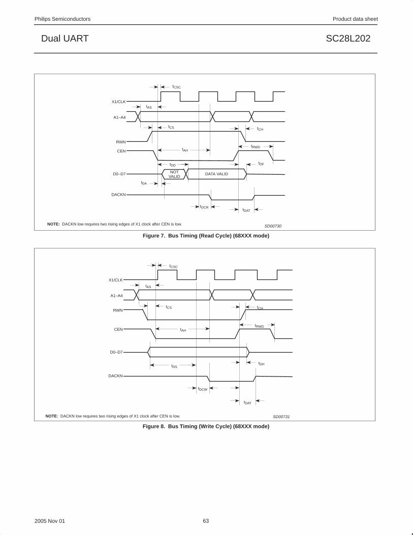
Philips Semiconductors Product data sheet
SC28L202Dual UART
2005 Nov 01 63
X1/CLK
A1–A4
RWN
CEN
D0–D7
DACKN
tCSC
tAS
tCS
tDF
tDAT
tCH
tRWD
tDD
tDCR
tAH
DATA VALIDNOTVALID
tDA
NOTE: DACKN low requires two rising edges of X1 clock after CEN is low. SD00730
Figure 7. Bus Timing (Read Cycle) (68XXX mode)
X1/CLK
A1–A4
RWN
CEN
D0–D7
DACKN
tCSC
tAS
tCS
tDH
tDAT
tCH
tRWD
tDS
tDCW
tAH
NOTE: DACKN low requires two rising edges of X1 clock after CEN is low. SD00731
Figure 8. Bus Timing (Write Cycle) (68XXX mode)

Philips Semiconductors Product data sheet
SC28L202Dual UART
2005 Nov 01 64
X1/CLK
INTRN
IACKN
D0–D7
DACKN
tCSC
tDD tDF
tDCR
tDATNOTE: DACKN low requires two rising edges of X1 clock after IACKN is low.
SD00732
Figure 9. Interrupt Cycle Timing (68XXX mode)
(b) OUTPUT PINS
RDN
IP0–IP6
WRN
OP0–OP7
tPS tPH
tPD
OLD DATA NEW DATA
(a) INPUT PINS
SD00135
Figure 10. Port Timing

Philips Semiconductors Product data sheet
SC28L202Dual UART
2005 Nov 01 65
NOTES:1. INTRN or OP3-OP7 when used as interrupt outputs.2. The test for open-drain outputs is intended to guarantee switching of the output transistor. Measurement of this response is referenced from the midpoint of the switching
signal, VM, to a point 0.2 V above VOL. This point represents noise margin that assures true switching has occurred. Beyond this level, the effects of external circuitry andtest environment are pronounced and can greatly affect the resultant measurement.
VM
VOL +0.2 V
VOL
WRN
INTERRUPT1
OUTPUT
tIR
VM
VOL +0.2 V
VOL
RDN
INTERRUPT1
OUTPUT
tIR
SD00735
Figure 11. Interrupt Timing (80xxx mode)
C1 = C2 ∼ 24 pF FOR CL = 13.5 pF. For the oscillator feedback loop the capacitors C1 and C2 are in series.
tCLKtCTCtRxtTx
X1/SCLKCTCLK
RxCTxC
tCLKtCTCtRxtTx
VCC
470 Ω
X1/Sclk
X2*
CLK
*NOTE: X2 MUST BE LEFT OPEN.
X2
14.7456 MHz
X1
C1
C2
SC28L202
NOTE:RESISTOR REQUIREDFOR TTL INPUT.
TO UARTCIRCUIT
TYP.160 kΩ
3 pF
3 pF
C1 and C2 should be chosen according to the crystal manufacturer’s specification.C1 and C2 values will include any parasitic capacitance of the wiring and X1 X2 pins.
2pF
4pF
Package capacitance approximately 4 pF.
SD00736
PARASITIC CAPACITANCE
PARASITIC CAPACITANCE
Figure 12. Clock Timing

Philips Semiconductors Product data sheet
SC28L202Dual UART
2005 Nov 01 66
tTXD
tTCS
1 BIT TIME(1 OR 16 CLOCKS)
TxD
TxC(INPUT)
TxC(1X OUTPUT)
SD00138
Figure 13. Transmitter External Clocks
tRXS tRXH
RxC(1X INPUT)
RxD
SD00139
Figure 14. Receiver External Clock
TRANSMITTERENABLED
TxD D1 D2 D3 D4 D6BREAK
TxRDY(SR2)
WRN
D1 D8 D9 D10 D12STARTBREAK
STOP BREAK
D11 WILLNOT BE
WRITTEN TOTHE TxFIFO
CTSN1
(IP0)
RTSN2
(OP0)
OPR(0) = 1 OPR(0) = 1NOTES:
1. Timing shown for MR2[4] = 1.
2. Timing shown for MR2[5] = 1. SD00155
Figure 15. Transmitter Timing

Philips Semiconductors Product data sheet
SC28L202Dual UART
2005 Nov 01 67
D1 D2 D8 D9 D10 D11 D12 D13RxD
D12, D13 WILL BE LOST DUE TO RECEIVER DISABLE.
RECEIVERENABLED
RxRDY(SR0)
FFULL(SR1)
RxRDY/FFULL(OP5)2
RDN
STATUS DATA
D1
STATUS DATA
D2
STATUS DATA
D3
STATUS DATA
D10D11 WILL BE LOSTDUE TO OVERRUNOVERRUN
(SR4) RESET BY COMMAND
RTS1
(OP0)
OPR[0] = 1NOTES:
1. Timing shown for MR1[7] = 1.
2. Shown for OPCR[4] = 1 and MR[6] = 0. SD00156
Figure 16. Receiver Timing
TRANSMITTERENABLED
TxD ADD#1
TxRDY(SR2)
WRN
MR1[4:3] = 11MR1[2] = 1
1
BIT 9
D0 0
BIT 9
ADD#2 1
BIT 9MASTER STATION
ADD#1 MR1[2] = 0 D0 MR1[2] = 1 ADD#2
RxD ADD#1 1
BIT 9
D0 0
BIT 9
ADD#2 1
BIT 9PERIPHERAL STATION
0
BIT 9
0
BIT 9
RECEIVERENABLED
RxRDY(SR0)
RDN/WRN
MR1[4:3] = 11 ADD#1 STATUS DATA
D0
STATUS DATA
ADD#2
SD00096
Figure 17. Wake-Up Mode

Philips Semiconductors Product data sheet
SC28L202Dual UART
2005 Nov 01 68
INTRNDACKN
D0–D7TxDA/B
OP0–OP7
85 pF
+5 V
I = 2.4 mA
85 pF
I = 2.4 mA VOL return to V CC for a 0 levelI = 400 µA VOH return to V SS for a 1 level
SD00733
Figure 18. Test Conditions on Outputs

Philips Semiconductors Product data sheet
SC28L202Dual UART
2005 Nov 01 69
TSSOP56: plastic thin shrink small outline package; 56 leads; body width 6.1 mm SOT364-1
Philips Semiconductors Product data sheet
SC28L202Dual UART
2005 Nov 01 70
REVISION HISTORY
Rev Date Description
_7 20051101 Product data sheet. Supersedes data of 16 April 2004 (9397 750 13049).
Modifications:
• Page 3, description for pin 21, I/M: changed “When HIGH or not connected configures the bus interface ...”to “When HIGH configures the bus interface ...:”
• Page 6, section “Bus Interface”, second sentence: changed “If this pin is high or left open ...” to “If this pin is HIGH ...”
• Page 34, UCIR — Update CIR; first sentence: changed “... address 0x8C.” to “... address 0x61.”
_6 20040416 Product data (9397 750 13049). Supersedes fifth version SC28L202_5 of 2002 Dec 03 (9397 750 10585).
_5 20031202 Product data (9397 750 10585). Supersedes fourth version SC28L202_4 of 2000 Feb 10 (9397 750 06826).
_4 20000210 Objective data (9397 750 06826).

Philips Semiconductors Product data sheet
SC28L202Dual UART
2005 Nov 01 71
DefinitionsShort-form specification — The data in a short-form specification is extracted from a full data sheet with the same type number and title. For detailed information seethe relevant data sheet or data handbook.
Limiting values definition — Limiting values given are in accordance with the Absolute Maximum Rating System (IEC 60134). Stress above one or more of the limitingvalues may cause permanent damage to the device. These are stress ratings only and operation of the device at these or at any other conditions above those givenin the Characteristics sections of the specification is not implied. Exposure to limiting values for extended periods may affect device reliability.
Application information — Applications that are described herein for any of these products are for illustrative purposes only. Philips Semiconductors make norepresentation or warranty that such applications will be suitable for the specified use without further testing or modification.
DisclaimersLife support — These products are not designed for use in life support appliances, devices, or systems where malfunction of these products can reasonably beexpected to result in personal injury. Philips Semiconductors customers using or selling these products for use in such applications do so at their own risk and agreeto fully indemnify Philips Semiconductors for any damages resulting from such application.
Right to make changes — Philips Semiconductors reserves the right to make changes in the products—including circuits, standard cells, and/or software—describedor contained herein in order to improve design and/or performance. When the product is in full production (status ‘Production’), relevant changes will be communicatedvia a Customer Product/Process Change Notification (CPCN). Philips Semiconductors assumes no responsibility or liability for the use of any of these products, conveysno license or title under any patent, copyright, or mask work right to these products, and makes no representations or warranties that these products are free from patent,copyright, or mask work right infringement, unless otherwise specified.
Contact informationFor additional information please visithttp://www.semiconductors.philips.com . Fax: +31 40 27 24825
For sales offices addresses send e-mail to:[email protected] .
Koninklijke Philips Electronics N.V. 2005All rights reserved. Printed in U.S.A.
Date of release: 11-05
Document order number: SC28L202_7
Data sheet status [1]
Objective data
Preliminary data
Product data
Productstatus [2] [3]
Development
Qualification
Production
Definitions
This data sheet contains data from the objective specification for product development.Philips Semiconductors reserves the right to change the specification in any manner without notice.
This data sheet contains data from the preliminary specification. Supplementary data will be publishedat a later date. Philips Semiconductors reserves the right to change the specification without notice, inorder to improve the design and supply the best possible product.
This data sheet contains data from the product specification. Philips Semiconductors reserves theright to make changes at any time in order to improve the design, manufacturing and supply. Relevantchanges will be communicated via a Customer Product/Process Change Notification (CPCN).
Data sheet status
[1] Please consult the most recently issued data sheet before initiating or completing a design.
[2] The product status of the device(s) described in this data sheet may have changed since this data sheet was published. The latest information is available on the Internet at URLhttp://www.semiconductors.philips.com.
[3] For data sheets describing multiple type numbers, the highest-level product status determines the data sheet status.
Level
I
II
III