scalable design rules revision
TRANSCRIPT

MOSIS Scalable CMOS Design Rules(revision 7)Jen-I Pithe MOSIS ServiceInformation Sciences InstituteUniversity of Southern California4676 Admiralty WayMarina del Rey, CA [email protected] 1, 19951 Introduction1.1 SCMOS Design RulesThis document de�nes the o�cial layout design rules for MOSIS scalable CMOS (SCMOS)design technology. It supercedes all previous revisions.In SCMOS technology, circuit geometries are drawn according to Mead and Conway's�-based methodology [3]. The unit of measurement, �, can easily be scaled to di�erentfabrication processes as semiconductor technology advances.A user design submitted to MOSIS in SCMOS technology should be in either CalmaGDSII format [1] or Caltech Intermediate Form (CIF version 2.0) [3]. Each design hasa technology designation that goes with it for the purpose of MOSIS's data prep. At themoment, three designations are used to specify CMOS processes. Each designation may haveone or more options associated for the purpose of either (1) special features for the targetprocess or (2) the presence of novel device in the design. At the time of writing, MOSIS iso�ering six CMOS processes from three di�erent foundries with drawn feature sizes rangingfrom 2.0 �m down to 0.6 �m.A list of the things that have either been revised or added since our last release can befound in Appendix A. Please refer to the speci�c sections for detailed descriptions.2 Standard SCMOSThe standard CMOS technology accessed by MOSIS is a single polysilicon, double metal,bulk CMOS process with enhancement-mode n-MOSFET and p-MOSFET devices [4].1

2.1 Well FlavorThree types of designation are used to indicate the avor of the well (substrate) used forfabrication as shown in Table 1.Designation DescriptionSCN Scalable CMOS N-wellSCP Scalable CMOS P-wellSCE Scalable CMOS Either-wellTable 1: SCMOS well avor designationsThe SCN and SCP designations with a submitted project are designed for fabricationof the speci�ed well only. For convenience, in both cases, a project may include the 'other'well, but it will always be ignored. SCE projects are used for fabrication in any CMOSprocess, N-well or P-well (either). A project with SCE designation must include both wells(and correspondingly, well/substrate contacts for proper bias). For any given fabricationprocess, the 'other' well will be ignored during the mask generation. If twin-tub processesare o�ered in the future, both wells will be used.2.2 SCMOS OptionsSCMOS options are used to designate projects which use additional layers beyond the stan-dard CMOS technology. Each option is named by a designator that is tacked onto the basicdesignator for its well avor. Reader should note that not all possible combinations (withwell avor) are actually available. The currently available SCMOS options are listed in Table2. In addition to the options in Table 2, two undeclared options also exist. One withrespect to the existence of high voltage MOSFET devices; the other, a tight metal rule forhigh-density metal interconnections. For options available to speci�c process, please refer toTable 3 for the current MOSIS o�erings.2.3 SCMOS O�eringsMOSIS is currently o�ering the fabrication processes as shown in Table 3. For each process,the list of appropriate SCMOS technology designations is listed. Note that whenever SCNxxappears in the table, SCExx is also appropriate. Likewise, whenever SCPxx appears, SCExxis also appropriate.2CCD layer not included.2CCD layer not included. 2

Designation Long form DescriptionE Electrode Adds a second polysilicon layer (electrode)that can serve as either one of electrode of a polycapacitor or as a gate for transistors. A contactlayer (electrode contact) to metal also exists.A Analog Adds electrode layer (as in E option) plus apbase layer for the construction of vertical NPNtransistor. A buried ccd layer is also present.for buried-channel CCD applications3M Triple Metal Adds second via (via2) and third metal (metal3)layers.LC Linear Capacitor Adds a cap well layer for the implementation oflinear capacitors.MEMS Micromechanical Adds two new layers, mems open andSystems mems etch stop for the purpose of micro-mechanical device construction.Table 2: SCMOS technology optionsFoundry Process Lambda OptionsOrbit 2.0 �m N-well 1.0 �m SCNA, SCNE, SCN, SCNA MEMSOrbit 2.0 �m P-well 1.0 �m SCPE, SCP, SCPE MEMSAMI 1.5 �m N-well 0.8 �m SCNA1, SCNE, SCN, High VoltageOrbit 1.2 �m N-well 0.6 �m SCNA2HP AMOSI/CMOS34 0.6 �m SCNLC, SCN, Tight MetalHP CMOS26B/G 0.5 �m SCN3M, SCN, Tight MetalTable 3: MOSIS SCMOS technology o�erings3

3 CIF and GDS Layer Speci�cationDesign geometries (or mask features) can be represented either in GDS-II or Caltech Inter-mediate Form (CIF Version 2.0). While the former is coded in binary format, the latter is aplain text �le and can be easily interpreted. For detailed syntax and semantic speci�cationsof Calma/GDS-II or CIF, please refer to [1] and [3] respectively.In GDS II format, a mask layer is speci�ed by a layer number between 0 and 63. MOSISnow reserves layers numberd from 21 to 62 for mask speci�cation and future extension.Layers de�ned out of this range can be used by customers for their own purpose. MOSISwill ignore all geometry information on these layers (0 to 20 and 63) and map it to the CIFcomment layer (CX) if necessary. In this revision, 6 new layers are added starting from layernumber 21.� CVP (layer 21) is used to indicate high-voltage p-type area. More comprehensiveinformation can be found in [2].� CVN (layer 22) is used to indicate high-voltage p-type area.� COP (layer 23) is used to indicate substrate pit opening area for MEMS devices.� CPS (layer 24) is used to indicate substrate p+ etching-stop area for MEMS devices.� CCC (layer 25) is used for generic contact.� XP (layer 26) is used to indicated pad location.Users should be aware that there exist only one type of physical contact (i.e. between�rst metal and poly or active), though several have been de�ned for historical reason andare retained for backward compatibility. A complete list of SCMOS layers can be found inTable 4 on next page.4 Sub-micron RulesThe SCMOS design rules have been historically designed for 1.0 - 3.0 micron CMOS tech-nology. To take full advantage of advanced submicron process technology, a set of rules havebeen selected to be modi�ed to �t our foundry's rules.Table 5 lists those rules in MOSIS's HP CMOS26G process that are di�erent betweenSCN3M and SCN3M 26G technology speci�cation with � equals to 0.5 and 0.4 �m respec-tively. 4

SCMOS layer CIF name GDS II number GDS II typeP HIGH VOLTAGE CVP 21 -N HIGH VOLTAGE CVN 22 -MEMS OPEN COP 23 -MEMS ETCH STOP CPS 24 -PADS XP 26 -P WELL CWP 41 -N WELL CWN 42 -ACTIVE CAA 43 -P PLUS SELECT CSP 44 -N PLUS SELECT CSN 45 -POLY CPG 46 -CONTACT CCC, CCP, CCA, CCE 25, 47, 48, 55 -METAL1 CMF 49 -VIA CVA 50 -METAL2 CMS 51 -GLASS COG 52 -ELECTRODE CEL 56 -BURIED CCD CCD 57 -PBASE CBA 58 -CAP WELL CWC 59 -VIA2 CVS 61 -METAL3 CMT 62 -COMMENT CX 0 - 20, 63 -Table 4: SCMOS technology CIF and GDS layers5
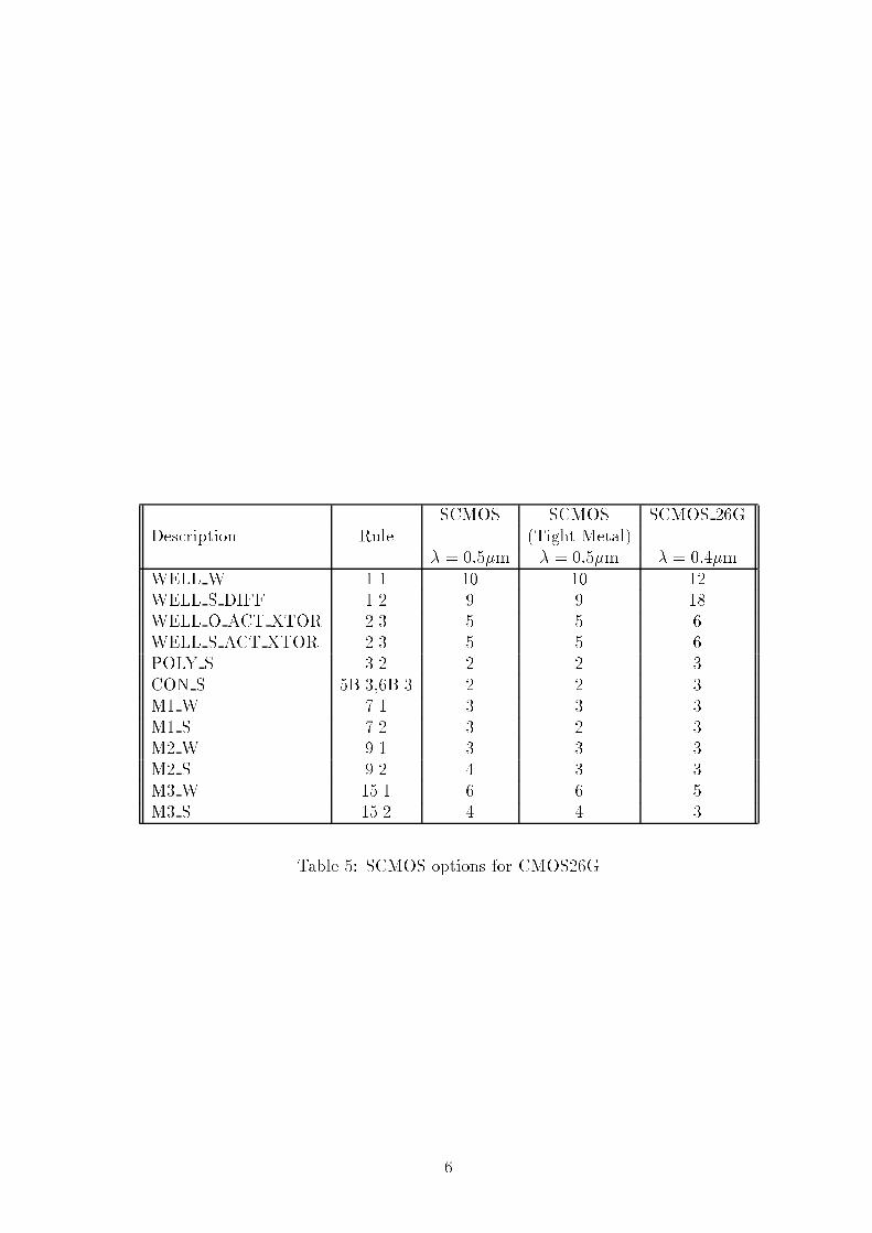
SCMOS SCMOS SCMOS 26GDescription Rule (Tight Metal)� = 0:5�m � = 0:5�m � = 0:4�mWELL W 1.1 10 10 12WELL S DIFF 1.2 9 9 18WELL O ACT XTOR 2.3 5 5 6WELL S ACT XTOR 2.3 5 5 6POLY S 3.2 2 2 3CON S 5B.3,6B.3 2 2 3M1 W 7.1 3 3 3M1 S 7.2 3 2 3M2 W 9.1 3 3 3M2 S 9.2 4 3 3M3 W 15.1 6 6 5M3 S 15.2 4 4 3Table 5: SCMOS options for CMOS26G6

5 SCMOS Design RulesWell (CWN, CWP)1.1 Minimum width 101.2 Minimum spacing between wells at di�erent potential 91.3 Minimum spacing between wells at same potential 0 or 61.4 Minimum spacing between wells of di�erent type(if both are drawn) 01.4
CWNCWNCWN
CWP
1.31.2
1.1
7

Active (CAA)2.1 Minimum width 32.2 Minimum spacing 32.3 Source/drain active to well edge 52.4 Substrate/well contact active to well edge 32.5 Minimum spacing between active of di�erent implant 0 or 4CAA
CAA CAA
CAA
CAA
CAA
CSP
CSP
CSN
CSN
_
region_
P
regionN
2.1
2.52.2
2.1
2.3 2.4
2.3 2.4
2.52.2
8

Poly (CPG)3.1 Minimum width 23.2 Minimum spacing 23.3 Minimum gate extension of active 23.4 Minimum active extension of ploy 33.5 Minimum �eld poly to active 1CAA
CPG
CPG
CAA
3.4
3.5
3.1
3.2
3.3
9

Select (CSN, CSP)4.1 Minimum select spacing to channel of transistor toensure adequate source/drain width 34.2 Minimum select overlap of active 24.3 Minimum select overlap of contact 14.4 Minimum select width and spacing 2(Note: P-select and N-select may be coincident, butmust not overlap)4.3
CCA
CSP CSN
CAA
CPG
CAA
CSPCSN
CWP CWN
4.3
4.2
4.1
10

Simple Contact to Poly (CCP)5.1.a Exact contact size 2 � 25.2.a Minimum poly overlap 1.55.3.a Minimum contact spacing 25.2.a
5.3.a
5.1.a
CCP
CPG
11

Simple Contact to Active (CCA)6.1.a Exact contact size 2 � 26.2.a Minimum active overlap 1.56.3.a Minimum contact spacing 26.4.a Minimum spacing to gate of transistor 26.3.a
6.2.a
6.4.a
6.1.a
CCA
CAA
CPG
CAA
12
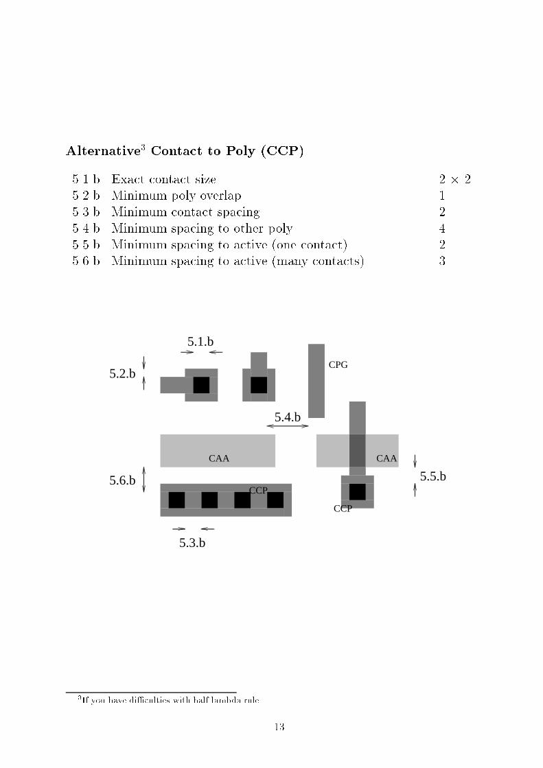
Alternative3 Contact to Poly (CCP)5.1.b Exact contact size 2 � 25.2.b Minimum poly overlap 15.3.b Minimum contact spacing 25.4.b Minimum spacing to other poly 45.5.b Minimum spacing to active (one contact) 25.6.b Minimum spacing to active (many contacts) 35.5.b
5.4.b
5.1.b
5.2.b
5.6.b
5.3.b
CCP
CCP
CAA
CPG
CAA
3If you have di�culties with half lambda rule. 13

Alternative4 Contact to Active (CCA)6.1.b Exact contact size 2 � 26.2.b Minimum active overlap 16.3.b Minimum contact spacing 26.4.b Minimum spacing to di�usion active 56.5.b Minimum spacing to gate of transistor 26.6.b Minimum sapcing to �eld poly (one contact) 26.7.b Minimum spacing to �eld poly (many contacts) 36.8.b Minimum spacing to poly contact 46.7.b
6.8.b6.2.b
6.1.b
6.6.b
6.5.b
6.3.b
6.4.b
CCA
CAA
CPG
CAA
4If you have di�culties with half lambda rule. 14

Metal1 (CMF)7.1 Minimum width 37.2.a Minimum spacing 37.2.b5 Minimum tight metal spacing 27.3 Minimum overlap of poly contact 17.4 Minimum overlap of active contact 1CCP
CCA
CPG
CAA
CMF
CMF
7.4
7.3
7.2
7.1
5Only allowed between minimum width wires, otherwise use regular spacing rule.15

Via1 (CVA)8.1 Exact size 2 � 28.2 Minimum via1 spacing 38.3 Minimum overlap by metal1 18.4 Minimum spacing to contact 28.5 Minimum spacing to poly or active edge 28.5
8.5CAA
CVA
CCA
CVA
CMSCMF
CAA
CPG 8.4
8.3
8.2
8.1
16

Metal2 (CMS)9.1 Minimum width 39.2.a Minimum spacing 49.2.b6 Minimum tight metal spacing 39.3 Minimum overlap of via1 19.2.a9.2.b
CMSCVA
CMS
CMF
9.3
9.1
6Only allowed between minimum width wires, otherwise use regular spacing rule.17
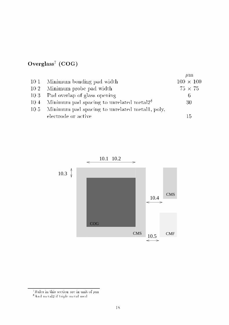
Overglass7 (COG) �m10.1 Minimum bonding pad width 100 � 10010.2 Minimum probe pad width 75 � 7510.3 Pad overlap of glass opening 610.4 Minimum pad spacing to unrelated metal28 3010.5 Minimum pad spacing to unrelated metal1, poly,electrode or active 15
CMS CMF
CMS
COG
10.5
10.4
10.3
10.210.1
7Rules in this section are in unit of �m.8And metal3 if triple metal used. 18

Electrode for Capacitor (CEL - Analog Option)11.1 Minimum width 311.2 Minimum spacing 311.3 Minimum poly overlap 211.4 Minimum spacing to active or well edge 211.5 Minimum spacing to poly contact 3CEL
CMF
CWNCPG
CEL
11.5
11.4
11.3
11.2
11.1
19

Electrode for Transistor (CEL - Analog Option)12.1 Minimum width 212.2 Minimum spacing 312.3 Minimum electrode gate overlap of active 212.4 Minimum spacing to active 112.5 Minimum spacing or overlap of poly 212.6 Minimum spacing to poly or active contact 3CEL
12.6
12.6CCA
CCE
12.2
12.5
12.4
12.3
12.1
CAA
CPG
CEL
20

Electrode Contact (CCE - Analog Option)13.1 Exact contact size 2 � 213.2 Minimum contact spacing 213.3 Minimum electrode overlap (on capacitor) 313.4 Minimum electrode overlap (not on capacitor) 213.5 Minimum spacing to poly or active 3
13.5
CPGCAA
13.5
13.4
13.3
13.2
13.1
CMF
CEL
CPG
CEL
21
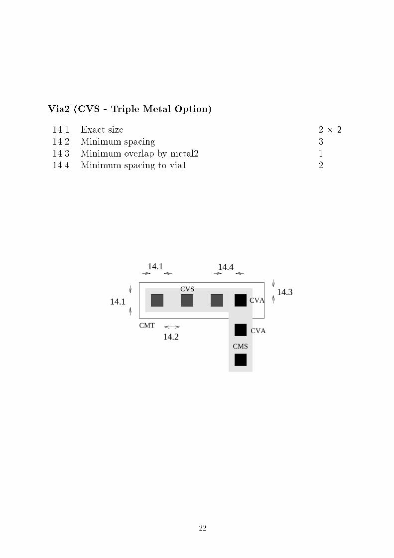
Via2 (CVS - Triple Metal Option)14.1 Exact size 2 � 214.2 Minimum spacing 314.3 Minimum overlap by metal2 114.4 Minimum spacing to via1 2CVA
CVS
CVA
CMS
CMT
14.3
14.414.1
14.1
14.2
22

Metal3 (CMT - Triple Metal Option)15.1 Minimum width 615.2 Minimum spacing to metal3 415.3 Minimum overlap of via2 215.1
15.3
15.2
CMT
CVSCMT
23

NPN Bipolar Transistor (CBA - Analog Option)16.1 All active contact 2 � 216.2 Minimum select overlap of emitter contact 316.3 Minimum pbase overlap of emitter select 216.4 Minimum spacing between emitter select and base select 416.5 Minimum pbase overlap of base select 216.6 Minimum select overlap of base contact 216.7 Minimum nwell overlap of pbase 616.8 Minimum spacing between pbase and collector active 416.9 Minimum active overlap of collector contact 216.10 Minimum nwell overlap of collector active 316.11 Minimum select overlap of collector active 2CCA CCACCA
CWN
CSN
CSN CSPCAA
CBA
16.11
16.10
16.9
16.8
16.7
16.6
16.516.4
16.3
16.2
16.1
24

Capacitor Well (CWC - Linear Capacitor Option)17.1 Minimum width 1017.2 Minimum spacing 917.3 Minimum spacing to external active 517.4 Minimum overlap of active 3CWPCWC
CAACWN
CWC
CAA
17.4
17.3 17.2
17.1
25

Linear Capacitor (Linear Capacitor Option)18.1 Minimum width 318.2 Minimum poly extension of active 118.3 Minimum active overlap of poly 318.4 Minimum poly contact to active 218.5 Minimum active contact to poly 4CCA
CWC
CAA
CPG
18.1
18.318.5
18.4
capacitor
linear
18.2
26

Buried Channel CCD (CCD - Analog Option9)19.1 Minimum CCD channel active width 419.2 Minimum CCD channel active spacing 419.3 Minimum CCD implant overlap of channel active 219.4 Minimum outside contact to CCD implant 319.5 Minimum select overlap of electrode (or poly) 219.6 Minimum poly/electrode overlap within channel active 219.7 Minimum contact to channel electrode (or poly) 219.5
19.7
19.7
19.1
19.4
19.2CAA
CSN
CELCEL
CPGCPG
CCD
CEL
CPG
CSN
CAA
19.6
19.5
19.4
19.3
19.1
9Not for all processes 27

References[1] Cadence Design Systems, Inc./Calma. GDSII Stream Format Manual, Feb. 1987. Release6.0, Documentation No.: B97E060.[2] J. Marshall, M. Gaitan, M. Zaghloul, D. Novotny, V. Tyree, J.-I. Pi, C. Pi~n�a, andW. Hansford. Realizing suspended structures on chips fabricated by CMOS foundryprocesses through the MOSIS service. Technical Report NISTIR-5402, National Instituteof Standards and Technology, U.S. Department of Commerce, Gaithersburg, MD, 1994.[3] C. Mead and L. Conway. Introduction to VLSI Systems. Addison-Wesley, 1980.[4] N. H. E. Weste and K. Eshraghian. Principles of CMOS VLSI Design: A System Per-spective. Addison-Wesley, 2nd. edition, 1993.
28