schottky diode integrated circuits for sub … of california santa barbara schottky diode integrated...
TRANSCRIPT

University of California
Santa Barbara
Schottky Diode Integrated Circuitsfor Sub-Millimeter-Wave Applications
A Dissertation submitted in partial satisfaction
of the requirements for the degree of
Doctor of Philisophy
in
Electrical and Computer Engineering
by
Scott Thomas Allen
Committee in charge:
Professor Mark Rodwell, Chairperson
Professor Steve Long
Professor Umesh Mishra
Professor Robert York
June 28, 1994

The dissertation of Scott Thomas Allen
is approved:
Committee Chairperson
July 29, 1993
ii

Copyright by
Scott Thomas Allen
1994
iii

Acknowledgments
First and foremost I would like to thank Professor Rodwell for being anadvisor, mentor, and friend to me during my graduate school career. Thequality of one’s experience in graduate school depends heavily on the advisor,and Professor Rodwell has made mine a rich and rewarding one. Withoutexception, I have found the faculty here at U.C. Santa Barbara to be of thehighest caliber, and my committee members, in particular, have contributedgreatly to my education.
My colleagues that have helped in my research efforts also deserve specialmention. The work of Mike Case and Masayuki Kamegawa laid the foun-dation on which my thesis project was based. Uddalak Bhattacharya andMadhukar Reddy deserve an extra expression of gratitude because they arepeople with whom I have worked the closest for the past two years. Every-one else with whom I have worked, Eric Carman, Kirk Giboney, YoshiyukiKonishi, Ruai Yu, and more recently, Bipul Agarwal and Rajasekhar Pullela,have contributed in a positive way to my experience here. My colleagues atthe Jet Propulsion Laboratory, Suzanne Martin and Peter Smith, also de-serve credit because without them the RTD project would never have cometo fruition.
I would especially like to thank my parents, Gary and Barbara, for in-stilling in me the value of education and for making the sacrifice to alwaysprovide their children with the best schooling available.
Most of all I would like to thank my loving wife, Sheri, for all the supportshe has given me for the last four years. She deserves my graduation morethan any one.
This research has been supported by the Air Force Office of ScientificResearch.
iv
Vita
• June 21, 1965: born in Long Beach, California
• May, 1987: B.S., with distinction, Electrical Engineering, Cornell Uni-versity
• February, 1989: M.S., Electrical and Computer Engineering, Universityof Massachusetts, Amherst
• 1987-1990: Design Engineer at the General Electric (now Martin Ma-rietta) Electronics Laboratory in Syracuse, NY
• August 4, 1990: married Sheri DeFrees
• 1990-1994: Research Assistant, Department of Electrical and ComputerEngineering, U.C. Santa Barbara
Publications
1. P. Ho, M.Y. Kao, P.C. Chao, K.H.G. Duh, J.M. Ballingall, S.T. Allen,A.J. Tessmer, and P.M. Smith, “Extremely High Gain 0.15 m Gate-Length InAlAs/InGaAs/InP HEMTs,” Electronics Letters, vol. 27, no.4, pp. 325-326, 14 Feb 1991.
2. P.M. Smith, P.C. Chao, P. Ho, K.H.G. Duh, M.Y. Kao, J.M. Ballingall,S.T. Allen, and A.J. Tessmer, “Microwave InAlAs/InGaAs/InP HEMTs:Status and Applications,” Proceedings of the Second International Con-ference on Indium Phosphide and Related Materials, Colorado, 1990.
3. D.W. Ferguson, S.T. Allen, M.Y. Kao, P.M. Smith, P.C. Chao, M.A.G.Upton, and J.M. Ballingall, “35 GHz Pseudomorphic HEMT MMICPower Amplifer,” 1991 IEEE MTT-S International Microwave Sympo-sium Digest, pp. 335-338, Boston, MA, June, 1991.
v
4. M. Kamegawa, K. Giboney, J. Karin, S. Allen, M.Case, R. Yu, M.J.W.Rodwell, and J.E. Bowers, “Picosecond GaAs Photodetector Mono-lithically Integrated with a High Speed Sampling Circuit,” IEEE/OSATopical Meeting on Picosecond Electronics and Optoelectronics, SaltLake City, Utah, March, 1991.
5. M. Kamegawa, K. Giboney, J. Karin, S. Allen, M.Case, R. Yu, M.J.W.Rodwell, and J.E. Bowers, “Picosecond GaAs Monolithic Optoelec-tronic Sampling Circuit,” Photonics Technology Letters, vol. 3, no. 6,pp. 567-569, June, 1991.
6. M. Rodwell, M. Kamegawa, M. Case, R. Yu, K. Giboney, E. Car-man, J. Karin, S. Allen, and Jeff Franklin, “Nonlinear TransmissionLines and their Applications in Picosecond Optoelectronic and Elec-tronic Measurements,” 1991 Engineering Foundation Conference onHigh Frequency/ High Speed Optoelectronics, Palm Beach, Florida,March, 1991.
7. Mark Rodwell, S. Allen, M. Kamegawa, K. Giboney, J. Karin, M. Case,R. Yu, and J.E. Bowers, “Picosecond Photodectectors MonolithicallyIntegrated with High-Speed Sampling Circuits,” AFCEA DoD FiberOptics Conference, March, 1992.
8. Y. Konishi, S.T. Allen, M. Reddy, M.J.W. Rodwell, R. Peter Smith andJohn Liu, “AlAs/GaAs Schottky-Collector Resonant-Tunnel-Diodes,”1992 Engineering Foundation Workshop on Advanced HeterostructureTransistors, Kona, Hawaii, November, 1992.
9. Y. Konishi, S.T. Allen, M. Reddy, R. Yu, M.J.W. Rodwell, R. Pe-ter Smith, and John Liu, “AlAs/GaAs Schottky-Collector Resonant-Tunnel-Diodes and Traveling-Wave Pulse Generators,” OSA Proceed-ings on Ultrafast Electronics and Optoelectronics, San Francisco, CA,January, 1993.
10. Y. Konishi , S.T. Allen, M. Reddy, M. J. W. Rodwell, R. Peter Smithand John Liu, “AlAs/GaAs Schottky-Collector Resonant-Tunnel-Diodes,”Solid-State Electronics, vol. 36, no. 12, pp. 1673-1676, December,1993.
11. M.J.W. Rodwell, M. Case, R. Yu, S. Allen, M. Reddy, U. Bhattacharya,and K. Giboney, “Ultrashort Pulse Generation Using Nonlinear Mi-
vi

crowave Transmission Lines,” Invited Presentation at the 1993 IEEE In-ternational Microwave Symposium, Workshop on Picosecond and Fem-tosecond Electromagnetic Pulses: Analysis and Applications, Atlanta,Georgia, June, 1993.
12. Ruai Yu, Madhukar Reddy, Joe Pusl, Scott Allen, Michael Case, andMark Rodwell, “Full Two-Port On-Wafer Vector Network Analysis to120 GHz Using Active Probes,” 1993 IEEE MTT-S International Mi-crowave Symposium Digest, pp. 1339-1342, Atlanta, Georgia, June,1993.
13. M.J.W. Rodwell, R. Yu, M. Reddy, S. Allen, M. Case, and U. Bhat-tacharya, “mm- Wave Network Analysis Using Nonlinear TransmissionLines,” Invited Presentation at the 14th Biennial IEEE/Cornell Univer-sity Conference on Advanced Concepts in High Speed SemiconductorDevices and Circuits, Cornell University, August, 1993.
14. M.J.W. Rodwell, S. Allen, M. Case, R. Yu, M. Reddy, U. Bhattacharya,and K. Giboney, “GaAs Nonlinear Transmission Lines for Picosecondand Millimeter-Wave Applications,” Invited Presentation at the 1993European Microwave Convention, Madrid, Spain, September, 1993.
15. Y. Konishi, M. Kamegawa, M. Case, R. Yu, S.T. Allen, and M. J. W.Rodwell, “A Broadband Free-Space Millimeter-Wave Vector Transmis-sion Measurement System”, Microwave Theory and Techniques, to bepublished (accepted April 30, 1993.)
16. S.T. Allen, U. Bhattacharya, and M.J.W. Rodwell, “4 THz Sidewall-Etched Varactors for Sub-mm-Wave Sampling Circuits,” 1993 IEEEGaAs IC Symposium Digest, pp. 285-287, San Jose, CA, October,1993.
17. S.T. Allen, M. Reddy, M.J.W. Rodwell, R.P. Smith, J. Liu, S.C. Martin,and R.E. Muller, “Submicron Schottky-Collector AlAs/GaAs ResonantTunnel Diodes,” 1993 International Electron Devices Meeting TechnicalDigest, pp. 407-410, Washington, D.C., December, 1993.
18. S.T. Allen, U. Bhattacharya, and M.J.W. Rodwell, “Multi-THz Sidewall-Etched Varactor Diodes and Their Application in Sub-mm-Wave Sam-pling Circuits,” Electronics Letters, vol. 29, no. 25, pp. 2227-2228, 9December 1993.
vii

19. M.J.W. Rodwell, S.T. Allen, R.Y. Yu, M.G. Case, U. Bhattacharya,M. Reddy, E. Carman, J. Pusl, M. Kamegawa, Y. Konishi, and R.Pullela, “Active and Nonlinear Wave Propagation Devices in UltrafastElectronics and Optoelectronics,” Proceedings of the I.E.E.E., invitedpaper, to be published.
20. Kirk S. Giboney, Scott T. Allen, Mark J.W. Rodwell, and John E. Bow-ers, “1.5 ps Fall-Time Measurements by Free-Running Electro-OpticSampling,” Conference on Lasers and Electro-Optics, Anaheim, CA,May, 1994.
21. R.Y. Yu, Y. Konishi, S.T. Allen, M. Reddy, and M.J.W. Rodwell,“A Traveling- Wave Resonant Tunnel Diode Pulse Generator,” Mi-crowave and Guided Wave Letters, to be published (accepted February10, 1994.)
22. S.T. Allen, M.J.W. Rodwell, R.Y. Yu, M.G. Case, E. Carman, M.Reddy, and Y. Konishi, “Nonlinear Wave Propagation Devices for Ultra-Fast Electronics,” invited paper, Second International Conference onUltra-Wideband, Short-Pulse Electromagnetics, Brooklyn, NY, April,1994.
23. R.E. Muller, S.C. Martin, R.P. Smith, S.T. Allen, M. Reddy, andM.J.W. Rodwell, “Electron Beam Lithography for the Fabrication ofAir-Bridged, Submicron Schottky Collectors,” International Sympo-sium on Electron, Ion and Photon Beams, New Orleans, LA, June,1994.
24. S.T. Allen, U. Bhattacharya, and Mark J.W. Rodwell, “725 GHz Sam-pling Circuits Integrated with Nonlinear Transmission Lines,” DeviceResearch Conference, Boulder, CO, June, 1994.
25. R.P. Smith, S.T. Allen, M. Reddy, S.C. Martin, J. Liu, R.E. Muller,and M.J.W. Rodwell, “0.1 m Schottky-Collector AlAs/GaAs ResonantTunneling Diodes,” Electron Device Letters, to be published (acceptedMay 3, 1994.)
viii

Abstract
Schottky Diode Integrated Circuits
for Sub-Millimeter-Wave Applications
byScott Thomas Allen
Using Schottky varactor diodes on GaAs, sampling circuits with band-widths of 725 GHz have been fabricated and measured. The sampling cir-cuits are integrated with nonlinear transmission lines, which are traveling-wave structures that generate the subpicosecond electrical pulses necessaryto strobe the sampling circuits. This bandwidth was obtained by combin-ing a number of technologies had been developed: varactor diodes with RCcutoff frequencies above 4 THz, coplanar waveguide transmission lines withthe center conductor elevated off the substrate, and ways of minimizing allparasitics. Other applications of these technologies include a 100 Gbit/secmux/demux circuit and 200 GHz traveling wave amplifiers.
By applying what had been learned from the varactor diodes, a noveldevice structure, a Schottky-collector resonant tunneling diode (RTD), wasdeveloped in the AlAs/GaAs system. By changing the collector from anohmic to a Schottky contact, the scaling laws that are used for other devicesare now applicable to the RTD. With 0.1 m Schottky fingers, a maximumfrequency of oscillation of 900 GHz was attained, more than twice that ofa conventional RTD. By applying this technique to AlAs/InGaAs on InP,RTDs with fmax above 2 THz have been tested. The long range goal of theproject is to build oscillator arrays for generating power above 1 THz.
ix

Contents
1 Introduction 1
2 Circuit Analysis and Design 52.1 Nonlinear Transmission Line Theory . . . . . . . . . . . . . . 5
2.1.1 Shock Wave Formation . . . . . . . . . . . . . . . . . . 62.1.2 Line Loss . . . . . . . . . . . . . . . . . . . . . . . . . 8
2.2 NLTL Design . . . . . . . . . . . . . . . . . . . . . . . . . . . 102.3 Sampling Circuits . . . . . . . . . . . . . . . . . . . . . . . . . 12
3 Schottky Varactor Diodes 193.1 Planar Diode Parasitics . . . . . . . . . . . . . . . . . . . . . . 193.2 Diode Fabrication . . . . . . . . . . . . . . . . . . . . . . . . . 26
3.2.1 Epitaxial Growth . . . . . . . . . . . . . . . . . . . . . 263.2.2 Ohmic Contacts . . . . . . . . . . . . . . . . . . . . . . 273.2.3 Proton Isolation . . . . . . . . . . . . . . . . . . . . . . 283.2.4 Schottky Contacts . . . . . . . . . . . . . . . . . . . . 313.2.5 Sidewall Etch . . . . . . . . . . . . . . . . . . . . . . . 313.2.6 Air Bridges . . . . . . . . . . . . . . . . . . . . . . . . 34
3.3 Diode Characterization . . . . . . . . . . . . . . . . . . . . . . 353.3.1 DC Measurements . . . . . . . . . . . . . . . . . . . . 363.3.2 Microwave Measurements . . . . . . . . . . . . . . . . 40
4 NLTL Characterization 474.1 Microwave Measurements . . . . . . . . . . . . . . . . . . . . . 474.2 Sampling Circuit Measurements . . . . . . . . . . . . . . . . . 524.3 Limitations . . . . . . . . . . . . . . . . . . . . . . . . . . . . 55
5 NLTLs With Air Bridged Transmission Lines 575.1 Process Development . . . . . . . . . . . . . . . . . . . . . . . 58
x

5.2 Electrical Characterization . . . . . . . . . . . . . . . . . . . . 625.3 Small Diodes . . . . . . . . . . . . . . . . . . . . . . . . . . . 655.4 NLTL Design . . . . . . . . . . . . . . . . . . . . . . . . . . . 665.5 Network Analyzer Data on NLTLs . . . . . . . . . . . . . . . 695.6 Measured Sampling Circuit Results . . . . . . . . . . . . . . . 705.7 Limitations . . . . . . . . . . . . . . . . . . . . . . . . . . . . 73
6 Future Development of NLTLs 756.1 Reaching 2 THz Bandwidth . . . . . . . . . . . . . . . . . . . 776.2 Diode Design . . . . . . . . . . . . . . . . . . . . . . . . . . . 786.3 Conclusion . . . . . . . . . . . . . . . . . . . . . . . . . . . . . 80
7 Schottky-Collector RTDs 837.1 Theory of RTD Operation . . . . . . . . . . . . . . . . . . . . 837.2 Increasing RTD Bandwidth . . . . . . . . . . . . . . . . . . . 887.3 Processing . . . . . . . . . . . . . . . . . . . . . . . . . . . . . 937.4 Measured Results . . . . . . . . . . . . . . . . . . . . . . . . . 96
8 Conclusion 1018.1 Air Bridged Transmission Lines . . . . . . . . . . . . . . . . . 1018.2 Future Development of SRTDs . . . . . . . . . . . . . . . . . . 103
A Design Files for Subpicosecond Shock Lines 105A.1 C Program for File Generation . . . . . . . . . . . . . . . . . . 105A.2 SPICE File . . . . . . . . . . . . . . . . . . . . . . . . . . . . 112A.3 Layout File . . . . . . . . . . . . . . . . . . . . . . . . . . . . 119
B Sampling Circuit SPICE File 127
C Detailed Process Flow 129
D Air Line Process Flow 151
E Air Line Generation Programs 173E.1 C Program . . . . . . . . . . . . . . . . . . . . . . . . . . . . . 173E.2 Line Parameters . . . . . . . . . . . . . . . . . . . . . . . . . . 180E.3 SPICE File . . . . . . . . . . . . . . . . . . . . . . . . . . . . 183E.4 Layout File . . . . . . . . . . . . . . . . . . . . . . . . . . . . 189E.5 Academy Macros . . . . . . . . . . . . . . . . . . . . . . . . . 191
xi

List of Figures
1.1 Historical development of sampling circuit technology . . . . . 2
2.1 NLTL schematic diagram . . . . . . . . . . . . . . . . . . . . . 62.2 Simulation of shock wave formation . . . . . . . . . . . . . . . 72.3 NLTL cell layout . . . . . . . . . . . . . . . . . . . . . . . . . 92.4 Effect of loss on compression . . . . . . . . . . . . . . . . . . . 112.5 Capacitance variation of Schottky diode . . . . . . . . . . . . 112.6 SPICE simulation of 0.68 ps edge . . . . . . . . . . . . . . . . 122.7 Sampling bridge . . . . . . . . . . . . . . . . . . . . . . . . . . 132.8 Balun/differentiator circuit . . . . . . . . . . . . . . . . . . . . 142.9 Schematic and equivalent circuit of balun . . . . . . . . . . . . 152.10 Sampling circuit . . . . . . . . . . . . . . . . . . . . . . . . . . 162.11 SPICE simulation of sampling circuit . . . . . . . . . . . . . . 172.12 Schematic diagram of test circuit . . . . . . . . . . . . . . . . 17
3.1 Planar diode . . . . . . . . . . . . . . . . . . . . . . . . . . . . 203.2 Schematic cross section of planar diode . . . . . . . . . . . . . 203.3 Distributed model of resistance under the Schottky contact . . 213.4 Large signal cutoff frequency for uniformly doped varactors . . 233.5 Equivalent circuit model of the diode including high frequency
effects . . . . . . . . . . . . . . . . . . . . . . . . . . . . . . . 253.6 Sidewall depletion under Schottky contact . . . . . . . . . . . 253.7 Cross section of a diode with sidewalls removed . . . . . . . . 263.8 C-V curves before and after sidewall etch . . . . . . . . . . . . 273.9 Damage profile from ion implantation . . . . . . . . . . . . . . 293.10 Photograph showing surface damage from polyimide . . . . . . 303.11 Implant mask . . . . . . . . . . . . . . . . . . . . . . . . . . . 303.12 Three step diode fabrication process . . . . . . . . . . . . . . . 323.13 Oxygen implant effect on diode capacitance . . . . . . . . . . 343.14 Air bridge process sequence . . . . . . . . . . . . . . . . . . . 35
xii

3.15 Reverse breakdown for N− = 1.0 · 1017 cm−3 . . . . . . . . . . 363.16 Reverse breakdown for N− = 3.0 · 1017 cm−3 . . . . . . . . . . 373.17 Linear I-V curves of a diode under forward bias . . . . . . . . 383.18 Log-linear plot of I-V curves of a diode under forward bias . . 383.19 J-V curves showing high Rs for small diodes . . . . . . . . . . 393.20 Effect of transverse straggle during ion implantation . . . . . . 403.21 Open standard for deembedding pad parasitics . . . . . . . . . 423.22 Short standard for deembedding pad parasitics . . . . . . . . . 433.23 Circuit model used to deembed the diode . . . . . . . . . . . . 433.24 Smith Chart plot of deembedded data of a small diode . . . . 443.25 Capacitance extraction for high frequency diode . . . . . . . . 453.26 Series resistance extraction using Y parameters . . . . . . . . 46
4.1 Measured S11 of NLTL . . . . . . . . . . . . . . . . . . . . . . 484.2 Measured S22 of NLTL . . . . . . . . . . . . . . . . . . . . . . 484.3 NLTL loss . . . . . . . . . . . . . . . . . . . . . . . . . . . . . 494.4 Measured delay . . . . . . . . . . . . . . . . . . . . . . . . . . 514.5 Cell layout . . . . . . . . . . . . . . . . . . . . . . . . . . . . . 524.6 SEM of shock on shock . . . . . . . . . . . . . . . . . . . . . . 534.7 SEM of 515 GHz sampler . . . . . . . . . . . . . . . . . . . . . 534.8 Measured 515 GHz response . . . . . . . . . . . . . . . . . . . 544.9 Two periods of measured signal . . . . . . . . . . . . . . . . . 55
5.1 Quasi-static simulation of CPW with center conductor in air . 585.2 Cross section of suspended air line . . . . . . . . . . . . . . . . 595.3 Air line process flow . . . . . . . . . . . . . . . . . . . . . . . 605.4 Details of polyimide flow . . . . . . . . . . . . . . . . . . . . . 615.5 Surface imaging photolithography . . . . . . . . . . . . . . . . 625.6 Cross section of air lines . . . . . . . . . . . . . . . . . . . . . 635.7 Measured and modeled S21 of air lines . . . . . . . . . . . . . 645.8 Measured and modeled phase of S21 of air lines . . . . . . . . 645.9 Measured and modeled S11 of air lines . . . . . . . . . . . . . 655.10 Cross section of small diode . . . . . . . . . . . . . . . . . . . 665.11 Perspective view of air line and Schottky diode . . . . . . . . . 675.12 S.E.M. of air line . . . . . . . . . . . . . . . . . . . . . . . . . 675.13 Loss mechanisms on the NLTL . . . . . . . . . . . . . . . . . . 695.14 Measured delay of air lines . . . . . . . . . . . . . . . . . . . . 705.15 Measured S11 and S22 of tapered impedance line . . . . . . . . 715.16 Measured S11 and S22 of an earlier design . . . . . . . . . . . . 71
xiii

5.17 S.E.M. of sampler with 1.0 µm x 1.0 µm diodes . . . . . . . . 725.18 Measurement of 725 GHz sampling circuit . . . . . . . . . . . 73
6.1 Three step doping profile . . . . . . . . . . . . . . . . . . . . . 766.2 Measured waveform from three step wafer . . . . . . . . . . . 776.3 Doping profile of proposed diode . . . . . . . . . . . . . . . . . 796.4 E-field profile of the proposed diodes at the punch-through
voltage . . . . . . . . . . . . . . . . . . . . . . . . . . . . . . 806.5 SPICE simulation of 170 fs shock wave . . . . . . . . . . . . . 81
7.1 Band diagram of RTD . . . . . . . . . . . . . . . . . . . . . . 847.2 I-V curve of an RTD . . . . . . . . . . . . . . . . . . . . . . . 857.3 Cross-sectional views of conventional RTD and SRTD . . . . . 867.4 Band diagrams of conventional RTD and SRTD . . . . . . . . 877.5 Band diagram of a Schottky diode and SRTD . . . . . . . . . 887.6 Equivalent circuit model of an RTD . . . . . . . . . . . . . . . 897.7 Cross-sectional diagram showing parasitics of SRTD . . . . . . 907.8 Dependence of fmax on collector contact width . . . . . . . . . 917.9 Electron transmission probability through double barrier . . . 927.10 Impact of quantum well lifetime on fmax . . . . . . . . . . . . 947.11 Side view of fabricated SRTD . . . . . . . . . . . . . . . . . . 957.12 S.E.M. of completed SRTD . . . . . . . . . . . . . . . . . . . . 957.13 Bias network for stabilizing RTDs . . . . . . . . . . . . . . . . 967.14 Measured I-V curve of SRTD . . . . . . . . . . . . . . . . . . 977.15 Measured SRTD capacitance at 0 V bias . . . . . . . . . . . . 987.16 Power output of network analyzer . . . . . . . . . . . . . . . . 997.17 Network analyzer measurement of SRTD . . . . . . . . . . . . 100
8.1 Schematic diagram of four diode bridge . . . . . . . . . . . . . 1028.2 Schematic diagram of traveling wave amplifier . . . . . . . . . 103
xiv

Contents
1 Introduction -1
2 Circuit Analysis and Design 3
2.1 Nonlinear Transmission Line Theory . . . . . . . . . . . . . . . . 3
2.1.1 Shock Wave Formation . . . . . . . . . . . . . . . . . . . . 4
2.1.2 Line Loss . . . . . . . . . . . . . . . . . . . . . . . . . . . 6
2.2 NLTL Design . . . . . . . . . . . . . . . . . . . . . . . . . . . . . 8
2.3 Sampling Circuits . . . . . . . . . . . . . . . . . . . . . . . . . . . 10
3 Schottky Varactor Diodes 17
3.1 Planar Diode Parasitics . . . . . . . . . . . . . . . . . . . . . . . . 17
3.2 Diode Fabrication . . . . . . . . . . . . . . . . . . . . . . . . . . . 24
3.2.1 Epitaxial Growth . . . . . . . . . . . . . . . . . . . . . . . 24
3.2.2 Ohmic Contacts . . . . . . . . . . . . . . . . . . . . . . . . 25
3.2.3 Proton Isolation . . . . . . . . . . . . . . . . . . . . . . . . 26
3.2.4 Schottky Contacts . . . . . . . . . . . . . . . . . . . . . . 29
3.2.5 Sidewall Etch . . . . . . . . . . . . . . . . . . . . . . . . . 29
3.2.6 Air Bridges . . . . . . . . . . . . . . . . . . . . . . . . . . 32
3.3 Diode Characterization . . . . . . . . . . . . . . . . . . . . . . . . 33
3.3.1 DC Measurements . . . . . . . . . . . . . . . . . . . . . . 34
3.3.2 Microwave Measurements . . . . . . . . . . . . . . . . . . 38
4 NLTL Characterization 45
4.1 Microwave Measurements . . . . . . . . . . . . . . . . . . . . . . . 45
4.2 Sampling Circuit Measurements . . . . . . . . . . . . . . . . . . . 50
4.3 Limitations . . . . . . . . . . . . . . . . . . . . . . . . . . . . . . 53
-5

-4 CONTENTS
5 NLTLs With Air Bridged Transmission Lines 555.1 Process Development . . . . . . . . . . . . . . . . . . . . . . . . . 565.2 Electrical Characterization . . . . . . . . . . . . . . . . . . . . . . 605.3 Small Diodes . . . . . . . . . . . . . . . . . . . . . . . . . . . . . 635.4 NLTL Design . . . . . . . . . . . . . . . . . . . . . . . . . . . . . 645.5 Network Analyzer Data on NLTLs . . . . . . . . . . . . . . . . . 675.6 Measured Sampling Circuit Results . . . . . . . . . . . . . . . . . 685.7 Limitations . . . . . . . . . . . . . . . . . . . . . . . . . . . . . . 71
6 Future Development of NLTLs 736.1 Reaching 2 THz Bandwidth . . . . . . . . . . . . . . . . . . . . . 756.2 Diode Design . . . . . . . . . . . . . . . . . . . . . . . . . . . . . 766.3 Conclusion . . . . . . . . . . . . . . . . . . . . . . . . . . . . . . . 78
7 Schottky-Collector RTDs 817.1 Theory of RTD Operation . . . . . . . . . . . . . . . . . . . . . . 817.2 Increasing RTD Bandwidth . . . . . . . . . . . . . . . . . . . . . 867.3 Processing . . . . . . . . . . . . . . . . . . . . . . . . . . . . . . . 917.4 Measured Results . . . . . . . . . . . . . . . . . . . . . . . . . . . 94
8 Conclusion 998.1 Air Bridged Transmission Lines . . . . . . . . . . . . . . . . . . . 998.2 Future Development of SRTDs . . . . . . . . . . . . . . . . . . . . 101
A Design Files for Subpicosecond Shock Lines 103A.1 C Program for File Generation . . . . . . . . . . . . . . . . . . . . 103A.2 SPICE File . . . . . . . . . . . . . . . . . . . . . . . . . . . . . . 110A.3 Layout File . . . . . . . . . . . . . . . . . . . . . . . . . . . . . . 117
B Sampling Circuit SPICE File 125
C Detailed Process Flow 127
D Air Line Process Flow 149
E Air Line Generation Programs 171E.1 C Program . . . . . . . . . . . . . . . . . . . . . . . . . . . . . . . 171E.2 Line Parameters . . . . . . . . . . . . . . . . . . . . . . . . . . . . 178E.3 SPICE File . . . . . . . . . . . . . . . . . . . . . . . . . . . . . . 181E.4 Layout File . . . . . . . . . . . . . . . . . . . . . . . . . . . . . . 187

CONTENTS -3
E.5 Academy Macros . . . . . . . . . . . . . . . . . . . . . . . . . . . 189

-2 CONTENTS

List of Figures
1.1 Historical development of sampling circuit technology . . . . . . . 0
2.1 NLTL schematic diagram . . . . . . . . . . . . . . . . . . . . . . . 42.2 Simulation of shock wave formation . . . . . . . . . . . . . . . . . 52.3 NLTL cell layout . . . . . . . . . . . . . . . . . . . . . . . . . . . 72.4 Effect of loss on compression . . . . . . . . . . . . . . . . . . . . . 92.5 Capacitance variation of Schottky diode . . . . . . . . . . . . . . 92.6 SPICE simulation of 0.68 ps edge . . . . . . . . . . . . . . . . . . 102.7 Sampling bridge . . . . . . . . . . . . . . . . . . . . . . . . . . . . 112.8 Balun/differentiator circuit . . . . . . . . . . . . . . . . . . . . . . 122.9 Schematic and equivalent circuit of balun . . . . . . . . . . . . . . 132.10 Sampling circuit . . . . . . . . . . . . . . . . . . . . . . . . . . . . 142.11 SPICE simulation of sampling circuit . . . . . . . . . . . . . . . . 152.12 Schematic diagram of test circuit . . . . . . . . . . . . . . . . . . 15
3.1 Planar diode . . . . . . . . . . . . . . . . . . . . . . . . . . . . . . 183.2 Schematic cross section of planar diode . . . . . . . . . . . . . . . 183.3 Distributed model of resistance under the Schottky contact . . . . 193.4 Large signal cutoff frequency for uniformly doped varactors . . . . 213.5 Equivalent circuit model of the diode including high frequency
effects . . . . . . . . . . . . . . . . . . . . . . . . . . . . . . . . . 233.6 Sidewall depletion under Schottky contact . . . . . . . . . . . . . 233.7 Cross section of a diode with sidewalls removed . . . . . . . . . . 243.8 C-V curves before and after sidewall etch . . . . . . . . . . . . . . 253.9 Damage profile from ion implantation . . . . . . . . . . . . . . . . 273.10 Photograph showing surface damage from polyimide . . . . . . . . 283.11 Implant mask . . . . . . . . . . . . . . . . . . . . . . . . . . . . . 283.12 Three step diode fabrication process . . . . . . . . . . . . . . . . . 303.13 Oxygen implant effect on diode capacitance . . . . . . . . . . . . 32
-1

0 LIST OF FIGURES
3.14 Air bridge process sequence . . . . . . . . . . . . . . . . . . . . . 333.15 Reverse breakdown for N− = 1.0 · 1017 cm−3 . . . . . . . . . . . . 343.16 Reverse breakdown for N− = 3.0 · 1017 cm−3 . . . . . . . . . . . . 353.17 Linear I-V curves of a diode under forward bias . . . . . . . . . . 363.18 Log-linear plot of I-V curves of a diode under forward bias . . . . 363.19 J-V curves showing high Rs for small diodes . . . . . . . . . . . . 373.20 Effect of transverse straggle during ion implantation . . . . . . . . 383.21 Open standard for deembedding pad parasitics . . . . . . . . . . . 403.22 Short standard for deembedding pad parasitics . . . . . . . . . . . 413.23 Circuit model used to deembed the diode . . . . . . . . . . . . . . 413.24 Smith Chart plot of deembedded data of a small diode . . . . . . 423.25 Capacitance extraction for high frequency diode . . . . . . . . . . 433.26 Series resistance extraction using Y parameters . . . . . . . . . . 44
4.1 Measured S11 of NLTL . . . . . . . . . . . . . . . . . . . . . . . . 464.2 Measured S22 of NLTL . . . . . . . . . . . . . . . . . . . . . . . . 464.3 NLTL loss . . . . . . . . . . . . . . . . . . . . . . . . . . . . . . . 474.4 Measured delay . . . . . . . . . . . . . . . . . . . . . . . . . . . . 494.5 Cell layout . . . . . . . . . . . . . . . . . . . . . . . . . . . . . . . 504.6 SEM of shock on shock . . . . . . . . . . . . . . . . . . . . . . . . 514.7 SEM of 515 GHz sampler . . . . . . . . . . . . . . . . . . . . . . . 514.8 Measured 515 GHz response . . . . . . . . . . . . . . . . . . . . . 524.9 Two periods of measured signal . . . . . . . . . . . . . . . . . . . 53
5.1 Quasi-static simulation of CPW with center conductor in air . . . 565.2 Cross section of suspended air line . . . . . . . . . . . . . . . . . . 575.3 Air line process flow . . . . . . . . . . . . . . . . . . . . . . . . . 585.4 Details of polyimide flow . . . . . . . . . . . . . . . . . . . . . . . 595.5 Surface imaging photolithography . . . . . . . . . . . . . . . . . . 605.6 Cross section of air lines . . . . . . . . . . . . . . . . . . . . . . . 615.7 Measured and modeled S21 of air lines . . . . . . . . . . . . . . . 625.8 Measured and modeled phase of S21 of air lines . . . . . . . . . . 625.9 Measured and modeled S11 of air lines . . . . . . . . . . . . . . . 635.10 Cross section of small diode . . . . . . . . . . . . . . . . . . . . . 645.11 Perspective view of air line and Schottky diode . . . . . . . . . . . 655.12 S.E.M. of air line . . . . . . . . . . . . . . . . . . . . . . . . . . . 655.13 Loss mechanisms on the NLTL . . . . . . . . . . . . . . . . . . . . 675.14 Measured delay of air lines . . . . . . . . . . . . . . . . . . . . . . 685.15 Measured S11 and S22 of tapered impedance line . . . . . . . . . . 69

LIST OF FIGURES 1
5.16 Measured S11 and S22 of an earlier design . . . . . . . . . . . . . . 695.17 S.E.M. of sampler with 1.0 µm x 1.0 µm diodes . . . . . . . . . . 705.18 Measurement of 725 GHz sampling circuit . . . . . . . . . . . . . 71
6.1 Three step doping profile . . . . . . . . . . . . . . . . . . . . . . . 746.2 Measured waveform from three step wafer . . . . . . . . . . . . . 756.3 Doping profile of proposed diode . . . . . . . . . . . . . . . . . . . 776.4 E-field profile of the proposed diodes at the punch-through voltage 786.5 SPICE simulation of 170 fs shock wave . . . . . . . . . . . . . . . 79
7.1 Band diagram of RTD . . . . . . . . . . . . . . . . . . . . . . . . 827.2 I-V curve of an RTD . . . . . . . . . . . . . . . . . . . . . . . . . 837.3 Cross-sectional views of conventional RTD and SRTD . . . . . . . 847.4 Band diagrams of conventional RTD and SRTD . . . . . . . . . . 857.5 Band diagram of a Schottky diode and SRTD . . . . . . . . . . . 867.6 Equivalent circuit model of an RTD . . . . . . . . . . . . . . . . . 877.7 Cross-sectional diagram showing parasitics of SRTD . . . . . . . . 887.8 Dependence of fmax on collector contact width . . . . . . . . . . . 897.9 Electron transmission probability through double barrier . . . . . 907.10 Impact of quantum well lifetime on fmax . . . . . . . . . . . . . . 927.11 Side view of fabricated SRTD . . . . . . . . . . . . . . . . . . . . 937.12 S.E.M. of completed SRTD . . . . . . . . . . . . . . . . . . . . . . 937.13 Bias network for stabilizing RTDs . . . . . . . . . . . . . . . . . . 947.14 Measured I-V curve of SRTD . . . . . . . . . . . . . . . . . . . . 957.15 Measured SRTD capacitance at 0 V bias . . . . . . . . . . . . . . 967.16 Power output of network analyzer . . . . . . . . . . . . . . . . . . 977.17 Network analyzer measurement of SRTD . . . . . . . . . . . . . . 98
8.1 Schematic diagram of four diode bridge . . . . . . . . . . . . . . . 1008.2 Schematic diagram of traveling wave amplifier . . . . . . . . . . . 101

2 LIST OF FIGURES

Chapter 1
Introduction
With the recent advances in the performance of high speed transistors [1], de-vice operating bandwidths have increased far beyond the available measuringinstrument bandwidth. This limits the ability to understand the high frequencyphysics of the devices and also makes it difficult to design circuits that can takeadvantage of their available bandwidth. To overcome this measurement limita-tion, sampling circuits with bandwidths exceeding those of the fastest transistorsare necessary.
The first necessary component of a high frequency sampling circuit is a strobesignal for the sampling bridge that has a pulse width much shorter than thetime response of the signal that is being sampled. The technology that enablesthe electrical generation of subpicosecond pulses is the nonlinear transmissionline (NLTL) [2]. An NLTL is formed in an integrated circuit on GaAs by usingreverse biased Schottky diodes as nonlinear capacitances to load down a coplanarwaveguide transmission line. The variable capacitance of the diodes results in avoltage dependent velocity for waves traveling on the NLTL, and this variablevelocity causes the falling edge of a signal to be compressed. The step functiongenerated by the NLTL can then be differentiated to form a pulse, and this pulseis used to strobe the sampling circuits.
The second component of a sampling circuit is the sampling bridge, whichcan be readily implemented with two Schottky diodes and two holding capacitors[3]. For this part of the circuit, it is the RC cutoff frequency of the diodesthat sets the frequency response. The overall sampling circuit bandwidth is theconvolution of the aperture time of the strobe pulse generated by the NLTL andthe RC time constant of the sampling bridge.
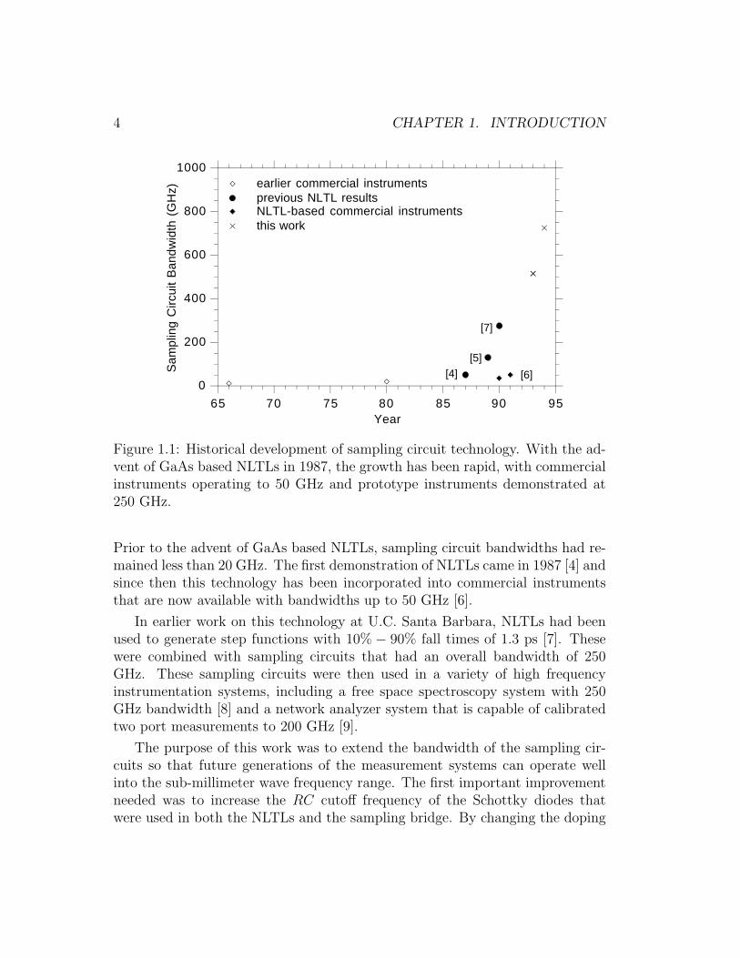
Figure 1.1 shows the historical development of sampling circuit technology.
3
0
200
400
600
Sam
plin
g C
ircui
t B
andw
idth
(G
Hz)
800
1000
65 70 75 80 85
earlier commercial instrumentsprevious NLTL results
Year
NLTL-based commercial instrumentsthis work
[4][5]
[6]
[7]
90 95
4 CHAPTER 1. INTRODUCTION
Figure 1.1: Historical development of sampling circuit technology. With the ad-vent of GaAs based NLTLs in 1987, the growth has been rapid, with commercialinstruments operating to 50 GHz and prototype instruments demonstrated at250 GHz.
Prior to the advent of GaAs based NLTLs, sampling circuit bandwidths had re-mained less than 20 GHz. The first demonstration of NLTLs came in 1987 [4] andsince then this technology has been incorporated into commercial instrumentsthat are now available with bandwidths up to 50 GHz [6].
In earlier work on this technology at U.C. Santa Barbara, NLTLs had beenused to generate step functions with 10% − 90% fall times of 1.3 ps [7]. Thesewere combined with sampling circuits that had an overall bandwidth of 250GHz. These sampling circuits were then used in a variety of high frequencyinstrumentation systems, including a free space spectroscopy system with 250GHz bandwidth [8] and a network analyzer system that is capable of calibratedtwo port measurements to 200 GHz [9].
The purpose of this work was to extend the bandwidth of the sampling cir-cuits so that future generations of the measurement systems can operate wellinto the sub-millimeter wave frequency range. The first important improvementneeded was to increase the RC cutoff frequency of the Schottky diodes thatwere used in both the NLTLs and the sampling bridge. By changing the doping

5
profiles of the diodes and scaling down their geometries, a substantial improve-ment in circuit speed was obtained: the NLTLs produced step functions with10%−90% fall times of 0.68 ps and the sampling circuits had bandwidths of 515GHz.
In order to extend the bandwidth even further, the other component of theNLTL, the coplanar waveguide, had to be improved. At extremely high frequen-cies, both the loss of the line and the phase velocity have a significant impacton the edge speed of the step function that is being generated. In order to ad-dress both of these issues, a novel coplanar waveguide structure was developed inwhich the center conductor was elevated off the semiconductor substrate. Oftenin high speed integrated circuits the interconnections are made with air bridgesin order to reduce the capacitive loading of the wiring. This concept was ex-tended even further for the NLTLs by having the center conductor for the entirelength of the transmission line suspended above the GaAs in order to simultane-ously reduce parasitics, reduce loss, and increase the electrical wavelength of thesignals. Coupling this air line technology with the high speed diodes resulted inNLTLs that generated step functions with 10%− 90% fall times of 0.48 ps andsampling circuits with 725 GHz bandwidth.
The limitation on the edge speed is now believed to be the saturation velocityof the electrons in the GaAs. The pulse formation on the NLTL occurs becausethe depletion edge of the Schottky diodes moves with changing reverse bias, andwith the step functions now being generated, it is the speed at which the deple-tion edge responds to the applied signal that is determining the edge speed. Thislimitation can be overcome by using diodes with more heavily doped layers, be-cause the distance that the depletion edge has to move for a given change in biasis inversely proportional to the doping level in the semiconductor. By increas-ing the doping in the diodes and extending the air bridged coplanar waveguidetechnique to air bridged microstrip lines, it should be feasible to fabricate 2 THzsampling circuits with only limited further technology development.
As a result of the studies on high frequency Schottky diodes, a new concept forresonant tunneling diodes (RTDs) was developed. It was found that by replacingthe ohmic collector contact of the conventional RTD with a Schottky contact, thescaling laws that were used to increase the frequency performance of the varactordiodes could also be applied to RTDs. By scaling the Schottky collector to deepsubmicron geometries using electron beam lithography, RTDs in the GaAs/AlAssystem were fabricated that had a maximum frequency of oscillation of 900 GHz,as computed from the measured dc and microwave parameters. By applyingthis same technique to the InGaAs/AlAs system on InP, RTDs with oscillation

6 CHAPTER 1. INTRODUCTION
frequencies as high as 3 THz are expected.The long range goal of the RTD technology is to fabricate oscillator arrays
operating at 1 THz. In order to accomplish this in an integrated circuit environ-ment, the air line technology developed for the NLTLs may be required becauseparastics can become dominant at such high frequencies. By making the contactto the RTDs with a line suspended in air, the parasitics are minimized becauseall the fringing fields are in air instead of the substrate, greatly reducing thecapacitance. This is another application of the air lines that demonstrates theirimportance as a technology for integrated circuits in the sub-millimeter wavefrequency range.
This dissertation is organized essentially in the chronological order of thedevelopment of the work. Chapter 2 discusses the theory of NLTLs and sam-pling circuits and shows some circuit simulations that were used in their design.Chapter 3 describes the details of the process flow and the dc and microwavecharacterization of the Schottky diodes. Chapter 4 discusses the initial 515 GHzresults and contains an analysis of what the limitations were. Chapter 5 explainsthe development of the air line technology and the 725 GHz sampling circuitsthat resulted from it, and chapter 6 contains a discussion of how the frequencyresponse can be further improved. Chapter 7 changes the focus and describesthe work on the Schottky-collector RTDs that was an outgrowth of the work onthe Schottky varactor diodes discussed in chapter 3. Chapter 8 summarizes theresults of this thesis project and outlines the directions of future developments.

Chapter 2
Circuit Analysis and Design
The nonlinear transmission lines and sampling circuits fabricated for this workwere integrated together on-wafer, so it was important to develop technologythat was applicable to both. The co-integration of the sampling circuits wasrequired because the electrical waveforms generated by the NLTLs had band-widths far exceeding those of any commercially available test instrument, so itwas necessary to also fabricate a measuring circuit with commensurate speed.Secondly, because one of the primary applications of these circuits is in mea-surement systems, it is the combined response of the NLTL and sampling circuitthat is of most significance.
The mathematics of the operation of NLTLs and their limitations was origi-nally worked out by Landauer [10] and later applied to GaAs integrated circuitsby Rodwell [2]. The discussion here about the NLTLs and sampling circuitsdraws heavily from the latter work.
2.1 Nonlinear Transmission Line Theory
NLTLs implemented on GaAs consist of sections of high impedance transmis-sion line periodically loaded with reverse-biased Schottky diodes that provide avoltage-variable capacitance to the system (figure 2.1 (a)). Figure 2.1 (b) showsthe equivalent circuit model for the line where Ll and Cl are the inductanceand capacitance per unit length of the line, respectively, and Cd and Rs are thecapacitance and series resistance of the varactor diodes.
7

Ll
Cl
Rs
Cd
(a)
(b)
8 CHAPTER 2. CIRCUIT ANALYSIS AND DESIGN
Figure 2.1: (a) Schematic diagram of NLTL. (b) Equivalent circuit model.
2.1.1 Shock Wave Formation
Because the capacitance of the diodes is a function of the voltage across them,the propagation delay of a wave traveling down the line, Td, is also a function ofthe voltage:
Td =√Ll · [Cl + Cd(V )] (2.1)
It is this dependence of propagation delay on voltage that leads to shock waveformation because the peak of the waveform, Vh, is traveling more slowly thanthe trough of the waveform, Vl, and so the falling edge of the wave is compressedas it propagates down the line. The SPICE simulation in figure 2.2 shows theevolution of a slow step function into a shock wave as it travels down the NLTL.The total compression of the line, ∆Td, is defined to be the difference in propa-gation delays for waves traveling with the minimum and maximum velocities:
∆Td = Td (Vh)− Td (Vl) (2.2)
The minimum fall time attainable can be derived from energy balance con-siderations on the transmission line [11] and is limited by the RsCd time constantof the Schottky diodes. For diodes with uniform doping the limit is
Tfall(10%− 90%) =8.8Cd(0)Rs√
1− (Vl/φbi)− 1(2.3)

Vh
Vl
-8
-6
-4
-2
0
2
0 50 100 150
Sim
ulat
ed R
espo
nse
(V)
Input Output
Time (ps)
2.1. NONLINEAR TRANSMISSION LINE THEORY 9
Figure 2.2: SPICE simulation showing the formation of a shock wave as it prop-agates down the NLTL.
For diodes with a doping level of ND = 1.0 ·1017 cm−3, a Schottky barrier heightof φbi = 0.8 V, and a Schottky contact width of 1 µm, CdRs = 76 fs and theminimum Tfall = 0.34 ps. This can be reduced to 0.25 ps by increasing thedoping level to 3.0 · 1017 cm−3; the details of the diode design will be discussedin chapter 3.
A number of useful parameters for the NLTL can be defined in terms of theaverage capacitance, or large signal capacitance, Cls, that the wave sees over itsentire voltage swing:
Cls =1
Vh − Vl
∫ Vh
Vl
Cd(V )dV (2.4)
This leads naturally to a definition for the large signal characteristic impedanceof the line, which is the effective loaded impedance of the NLTL under largesignal drive:
Zls =
√Ll
Cl + Cls(2.5)
If Zls = Zload then the shock wave is passed to the load without reflection ordistortion; and similarly, if Zls = Zgen then the signal from the generator islaunched on the NLTL with no reflection.

10 CHAPTER 2. CIRCUIT ANALYSIS AND DESIGN
One of the other limitations on the shock edge speed besides the diode RsCdtime constant is that because of the periodic nature of the line, there is a Braggfrequency above which energy cannot propagate, analogous to the forbiddenelectron energy bands in a periodic crystal. The Bragg frequency, fBr, is definedin terms of Cls as [2]
fBr =1
π√Ll · (Cl + Cls)
(2.6)
The ringing that can be seen on the waveform in figure 2.2 is at fBr becauseat this frequency all the energy is reflected and strong standing waves form.It is important in the design of the NLTL to keep fBr well above the highestfrequency at which there would be any significant energy.
2.1.2 Line Loss
There are two contributions to the loss of an NLTL, the loss from the diodes andthe resistive loss in the transmission line. There is no radiation loss because thecapacitive loading of the diodes is large enough that the wave veloctiy on theNLTL is slower than it would be in the GaAs so no energy can be coupled intoa substrate mode. The loss per section of NLTL is given by:
S21 = exp
[−ω2C2
lsRsZls2
− Rl
2Zls
](2.7)
The first term in the loss expression is the effect of the resistive loading ofthe diodes. The power loss from a shunt conductance loading on a transmissionline, Gload, is given by the simple expression e−Z0Gload . In order to calculate theeffect of the diode loading on the NLTL, a series to parallel transformation ismade to find the real part of the input admittance of the diode, which yieldsthe term ω2C2
lsRs in equation 2.7. In order to make this component of the losssmall, the RC cutoff frequency of the diode needs to be made high; chapter 3contains a detailed discussion of this diode optimization.
The second term in the equation for loss on the NLTL is from the resistiveloss on the metal transmission line, Rl, which can become quite significant athigh frequencies where the skin depth is small. There are a number of designstrategies that can be employed to minimize this component of the loss.
The first is to determine an impedance for the unloaded coplanar waveguide(CPW) that will minimize the overall loss. As the intrinsic capacitance of theCPW line becomes small compared to the capacitance of the loading diodes, the

w
dg
2.1. NONLINEAR TRANSMISSION LINE THEORY 11
Figure 2.3: Layout of NLTL cell. The length of the cell, d, is reduced to increasefBr, and all other parameters are scaled proportionately.
amount of compression for the wave increases (equation 2.1), so the length ofthe line decreases. The tradeoff is that as the impedance of the interconnectingsections of transmission lines is increased, the width of the center conductor ofthe CPW decreases, increasing its resistive loss. It was found in earlier studiesthat a line impedance of Zl = 75 Ω minimizes the line loss [12].
The second design feature on which to concentrate is the cell layout for eachsection of the NLTL. Figure 2.3 shows two cells on the NLTL. This figure does notshow the cross-over air bridges that tie the two ground planes together becausethey are not an integral part of the NLTL design but are necessary to preventunwanted modes from propagating on the ground planes. The inductance andcapacitance of the line for each section are Ll = Zld/vcpw and Cl = d/(Zlvcpw),where d is the spacing between the diodes and vcpw is the wave velocity on thecoplanar line. As d is reduced, the area of the diode is also reduced proportion-ately to maintain a constant Zls, and so fBr increases as 1/d. The tradeoff is thatas d is reduced to increase fBr, the horizontal dimensions of the cell must also bedecreased to maintain a reasonable length-to-width aspect ratio of d > (2g+w);otherwise, the sections of interconnecting metal could not legitimately be mod-eled as sections of transmission line.

12 CHAPTER 2. CIRCUIT ANALYSIS AND DESIGN
In coplanar waveguide, the line impedance is a function of the ratio of thecenter conductor width to the separation between the ground planes, and onGaAs is given by [13]:
Zl = 11.3Ω · ln(
21 + 4√
1− k2
1− 4√
1− k2
)(2.8)
where k = w/(w + 2g), so as g decreases, w must decrease proportionatelyand the resistive loss in the center conductor goes up. Because of this tradeoffbetween Rl and fBr, the correct design strategy is to make fBr no higher thanis necessary for each cell. At the input end of the line, where the harmoniccontent of the shock wave is relatively low, fBr can also be low and so the cellcan be large. The cell size can then be tapered along the line to accommodatethe increasing harmonics of the shock wave, and thus the center conductor isnever any narrower than necessary and Rl is minimized. The edge speed of theshock wave on the line decreases in proportion to the distance it has travelled,so the harmonic content of the signal is increasing at the inverse of this. In orderto accomodate this the Bragg frequency of the NLTL is increased exponentiallydown the line.
Reducing loss on the NLTL is extremely important because the effect is morethan just to decrease the amplitude of the signal on the line. A more subtle effect,but one that can be even more detrimental to the edge speed of the shock wave,is that as the amplitude decreases, the peak of the wave is no longer near 0 V.This is illustrated by figure 2.4 which shows how the signal decays and remainscentered about the negative dc bias applied to the line. The problem with thisis that the region of strong nonlinearity for the diodes is near 0 V (figure 2.5),so as the size of the signal decreases, the compression on the line is also reducedbecause the fractional change in capacitance seen by the signal is smaller. Tocompensate for this loss in compression, the NLTL must be made longer, whichcompounds the problem.
2.2 NLTL Design
The first shock lines designed for this work were based on diodes with 1 µm wideSchottky contacts and a doping of ND = 1.0 · 1017 cm−3. These diodes had areverse breakdown voltage of -12 V and a 3:1 change in capacitance for reversebias swing of 0 to -6 V; the details of the diode design will be discussed in thenext chapter. The CPW used for the interconnects was chosen to be 75 Ω in

-6
-5
-4
-3
-2
-1
0S
igna
l Le
vel
(V)
0 1000 2000 3000 4000 5000
Region ofstrong ∆C
Distance (µm)
0.0
0.2
0.4
0.6
0.8
1.0
0 1 2
C(V
)/C
(0V
)
3 4 5 6Reverse Bias (Volts)
2.2. NLTL DESIGN 13
Figure 2.4: The loss on the line results in the signal not swinging all the way to0 V, so the strong nonlinearity of the diodes in this region is not seen.
Figure 2.5: Reverse bias C-V characteristics of a uniformly doped diode showingthat the capacitance varies most rapidly near 0 V.

-7
-6
-5
-4
-3
-2
-1
0S
imul
ated
Sho
ck W
ave
(V)
0.0 1.0 2.0 3.0 4.0 5.0 6.0 7.0 8.0Time (ps)
0%
100%
Simulated 10% to 90%fall time=0.68 ps
14 CHAPTER 2. CIRCUIT ANALYSIS AND DESIGN
Figure 2.6: SPICE simulation of the designed NLTL showing an output fall timeof 0.68 ps.
order to minimize the power loss on the NLTL from the metallic losses in thecenter conductor. In order to keep the lines short to further reduce loss, a drivefrequency of 30 GHz was chosen because the faster the fall time of the inputsignal, the less compression the lines need. The Bragg frequency was taperedexponentially from an initial value of 250 GHz to a final value of 800 GHz at theoutput end of the line. The large signal impedance of the line was chosen to be40 Ω. This is close enough to the 50 Ω system impedance that power loss due tomismatch is negligible, 2%, but has the advantage of increasing the compressionof the line by the ratio 50/40. Appendix A contains the computer program thatwas used to generate the SPICE file and the layout file for these lines. Thesimulated waveform from SPICE, shown in figure 2.6, has Tfall = 0.68 ps.
2.3 Sampling Circuits
The sampling circuits were designed to be as synergistic with the NLTLs as pos-sible. The samplers consist of three components: a two-diode sampling bridge, abalun/differentiator, and an NLTL strobe pulse generator. The resistors in thesamplers were designed using the N+ buried layer of the Schottky diodes and

Chold
Chold
RIF
RIF
Z0 Z0
IF Output
IF Output
Signal Input
2.3. SAMPLING CIRCUITS 15
Figure 2.7: Schematic diagram of two diode sampling bridge.
the capacitors were implemented with reverse biased diodes, so no new masklayers were required.
Figure 2.7 is a schematic diagram of the two diode sampling bridge. Theinput signal is first attenuated to a level compatible with diode sampling and isthen applied through a 50 Ω transmission line to the node between the two sam-pling diodes, which are normally off, and is terminated with a 50 Ω load. Whenthe diodes are momentarily driven into forward conduction by the symmetricstrobe pulses, the input signal partially charges the hold capacitors. If the repe-tition frequency of the input signal is a multiple of the strobe frequency, at eachsuccessive strobe interval the sampling diodes will further charge the holdingcapacitors and cause the output voltage, sampled through the IF resistors, toasymptotically approach that of the input voltage. If the repetition frequency ofthe strobe signal is offset from that of the test signal by ∆f , then the sampledwaveform is mapped out in equivalent time at a repetition rate of ∆f .
The strobe pulse for the sampling circuits is generated using the output of anNLTL and a balun/differentiator network. A balun is a network that converts abalanced signal to an unbalanced one and vice versa and is required here becausesymmetric positive and negative strobe pulses are needed to gate the samplingdiodes. A differentiator is needed to convert the step function output of theNLTL into a pulse. Figure 2.8 shows the layout of the circuit that accomplishesboth of these functions.
The NLTL implemented in CPW intersects a coplanar strip line (CPS) at aright angle. The ground planes of the CPW are connected to one conductor ofthe CPS and the center conductor of the CPW is connected through a 50 Ω load

CPW Line
G S G
Coplanar Strip
+dshort
(NLTL Input)
Air Bridge
Sampling Diodes
CouplingCapacitors
16 CHAPTER 2. CIRCUIT ANALYSIS AND DESIGN
Figure 2.8: Balun/differentiator circuit that is used to convert the step functionof an NLTL into symmetric strobe pulses for the sampling diodes.
to the other conductor of the CPS. The CPS lines are shorted at equal distancesfrom the CPW center conductor so that the CPW line is loaded symmetrically.
The simplest way to analyze the circuit is to look at the two constituent piecesindependently. First consider the balun network that couples the CPW signalto the balanced CPS line. The shorted lines are acting as inductive stubs inthe ground planes of the CPW and the CPS modes are generated by the returncurrents of the CPW. The schematic diagram of this is shown in 2.9 (a) andthe equivalent circuit model for is shown in figure 2.9 (b). From the equivalentcircuit, the amplitude of the pulse across the stubs can be found:
Vpulse =Zstub/2
Rgen + ZO + Zstub/2Vgen (2.9)
Since it is difficult to make the impedance of CPS line on GaAs much higherthan 100 Ω, the amplitude of the pulse is limited to 1/3 of Vgen. By addingthe coupling capacitor Cc to the network, high frequency signals bypass the loadresistor and the voltage of the pulse is increased. The value of Cc is determinedusing SPICE to simulate the sampling circuit and is chosen as a compromisebetween the size of the strobe pulse and the size of the reflection back to theNLTL.

Shorted CPS
CPW ZO CC
ZO
CC
Vgen
RgenVpulse
Zstub
(a) (b)
2.3. SAMPLING CIRCUITS 17
Figure 2.9: (a) Schematic diagram of the balun showing the CPS as an inductivestub in the CPW ground return. (b) Equivalent circuit.
To understand the differentiation, consider the CPS lines alone. Since theyare short circuited, the forward traveling step functions are reflected back withreversed polarities and pulses are formed by the superposition of the forward andreflected waves. With the short placed at a distance dshort away from the planeof the sampling diodes, an impulse is generated at the diodes of a duration equalto the round-trip delay trt = 2dshort/vcpw. Because the CPS lines are terminatedin the 50 Ω of the NLTL, multiple strobe pulses do not occur.
The sampling bridge and the differentiator are combined into a compactlayout by using the ground planes of the CPW signal line as the coplanar striplines for the strobe signal. Using reverse biased diodes for the hold and couplingcapacitors and air bridges for the crossovers, as shown in figure 2.10, the entiresampling circuit can be implemented in a layout that is suitable for use withsub-millimeter waves.
The sampling circuit rise time is determined by the signal line RC timeconstant and the aperture time of the strobe pulse. The two sampling diodesload the signal line in parallel, so the 10% to 90% rise time is
TRC = 2.2 ·(Z0 +Rs
2
)· 2Cd (2.10)
The aperture time is determined by a combination of the fall time of the shockwave from the NLTL, the round trip delay of the shorted-line differentiatingnetwork, the sampling diode capacitance, and the amount of reverse bias on thesampling diodes. The round-trip time of the differentiator should be approxi-mately equal to the fall time of the shock wave. Larger round-trip times broadenthe strobe pulse while shorter times reduce the amplitude without significantlyreducing the impulse duration.

NLTL Strobe
Signal Input
Symmetric Short
Sampling Bridge
Short Circuit for Differentiator
18 CHAPTER 2. CIRCUIT ANALYSIS AND DESIGN
Figure 2.10: The sampling bridge and differentiator are combined in a compactlayout that is suitable for use with sub-millimeter waves.
In the absence of sampling diode parasitics to broaden the strobe pulse du-ration, it will have a full width at half maximum, FWHM, equal to the NLTLoutput fall time. Increasing the diode reverse bias decreases the duration of theforward conduction, and with a reverse bias that approaches the peak amplitudeof the strobe pulse, the aperture time can be reduced to a fraction of the impulseduration. Figure 2.11 is a SPICE simulation that shows a 0.14 ps aperture timefor the sampling circuit. The circuit file used for the simulation can be found inAppendix B, and uses a strobe pulse with a 10% to 90% fall time of 1.0 ps, adifferentiator round trip time of 1.0 ps, sampling diodes with 3 fF of capacitanceeach, and a reverse bias of 1 V.
A schematic diagram of the circuit used for testing is shown in figure 2.12.The signal being tested comes from one NLTL and a second NLTL is used tostrobe the sampling diodes. The measured signal is then the convolution of theshock wave on the NLTL and the pulse response of the sampling circuit. Becausethese are both limited by the same diode RC time constants, it is usually a goodapproximation to assume that their contributions to the measured signal areequal, and so it is straightforward to calculate a deconvolved shock edge speedand sampling circuit bandwidth.

-0.2
0
0.2
0.4
0.6
0.8
1S
ampl
ing
Dio
de C
urre
nt(m
A)
0.8 1.0 1.2 1.4 1.6 1.8Time (ps)
2.0
TFWHM=0.14 ps
SampledOutputs
Strobe NLTL
Sampling Circuit
NLTL Pulse Generator Under Test
2.3. SAMPLING CIRCUITS 19
Figure 2.11: SPICE simulation of the sampling circuit showing the aperture timeof the strobe pulse.
Figure 2.12: Schematic diagram of test circuit showing one NLTL as the testsignal and a second NLTL as the strobe signal.

20 CHAPTER 2. CIRCUIT ANALYSIS AND DESIGN

Chapter 3
Schottky Varactor Diodes
Schottky diodes are used in a number of millimeter wave and sub-millimeter waveapplications. They are used to both generate and receive signals at frequenciesabove the operational range of transistors. As mixer diodes, they have beenused to detect signals as high as 25 THz [14]. Their other common applicationis as multipliers, where the nonlinearity of their C-V curve is used to generateharmonics to produce power at frequencies unattainable directly with a solidstate oscillator, typically used in the 300 GHz to 1 THz range [15]. For usein NLTLs, it is this nonlinearity of their C-V curve under reverse bias thatis important because it is the variable capacitance that produces the variablepropagation delay for a wave traveling down the line. In designing a varactorfor this application, both the nonlinearity of the capacitance and the RC cutofffrequency of the diode are of primary concern.
3.1 Planar Diode Parasitics
A brief discussion of the diode fabrication is warranted at the outset because theparasitics of the diode are a function of its geometry and physical implementa-tion. The planar diode is designed specifically for ease of integration into circuitswhere the devices must be densely packed. Figure 3.1 shows a cross-sectionalview of the planar Schottky diode that was fabricated for this work. It consistsof a Schottky contact to an N− active region and recessed ohmic contacts to aheavily doped buried N+ layer. Areas outside where the diodes will be are ren-dered semi-insulating with a proton implantation. The active area of the diodesare defined by the intersection of the Schottky metal and the regions protectedduring the proton implantation. With this diode geometry the circuit layout is
21

Semi-Insulating GaAs Substrate
Buried N+ Layer
Ohmic Ohmic
Schottky
D DW
Tund
Semi-Insulating Substrate
D DW
Ohmic OhmicN- Layer
N+ Layer
Cdepl
RN
Rspr
2Roc 2Roc
2Rbl 2Rbl
22 CHAPTER 3. SCHOTTKY VARACTOR DIODES
Figure 3.1: Cross section of a planar Schottky diode fabricated for use in a highfrequency integrated circuit.
Figure 3.2: Schematic cross section of a planar diode illustrating the variouscomponents of the series resistance.
compact and the extrinsic parasitics are minimized, which is important for highfrequency operation in integrated circuits.
Figure 3.2 shows a cross-sectional schematic of a planar diode and its associ-ated equivalent circuit elements when under reverse bias. The Schottky contacthas width W , the diode stripe length into the plane of the page is L, and theseparation between the Schottky and ohmic contacts is D. The capacitance un-der the Schottky contact, C = εWL/d, is from the depleted space charge region,whose depth, d, is a function of the applied reverse bias:
d =
√√√√ 2ε
qND
·(Vbi − Vbias −
kT
q
)(3.1)
The resistance in series with this capacitance, Rs, can be modeled as the sumof four components. The first element, RN−, is the vertical resistance through

Cd
RN
Rspr
Cd
RN
Rspr
Cd
RN
Rspr
Cd
RN
Rspr Rspr
Schottky Contact
3.1. PLANAR DIODE PARASITICS 23
Figure 3.3: Schematic diagram illustrating the distributed nature of the resis-tance underneath the Schottky contact.
the undepleted portion of the N− active layer. While the amount of undepletedmaterial will be a function of bias, the value at 0 V bias is used as a conservativevalue because this will be the largest resistance:
RN− =1
WL· ρN− · Tund (3.2)
where ρN− is the resistivity of the material in the N− active layer and Tund isthe thickness of the undepleted region at 0 V bias. Because this resistance is avertical resistance, it is an area term and so is inversely proportional to WL.
The second component of the series resistance is the spreading resistance,Rspr, that accounts for the spreading of the current flow under the Schottkycontact into the buried N+ layer:
Rspr =1
12· WL· ρN+
TN+
(3.3)
where ρN+ is the resistivity of the N+ layer and TN+ is the thickness of thelayer. A factor of W/4 comes from the fact that the current will travel onlyhalf the contact width as it spreads out to either side and that these resistancesare in parallel. An additional factor of 1/3 arises from the distributed nature ofthe capacitance and resistance under the contact (figure 3.3) that is analogousto the spreading resistance in the base of a bipolar transistor or the distributedresistance of the gate finger of a MESFET.
The third component, Rbl, comes from the resistance of the buried layer dueto the separation between the Schottky and ohmic contacts:
Rbl =1
2· DL· ρN+
TN+
(3.4)

24 CHAPTER 3. SCHOTTKY VARACTOR DIODES
and again the factor of 1/2 arises because there are two in parallel. The finalcomponent of the series resistance, Roc, is from the ohmic contacts:
Roc =1
2L
√ρcont ·
ρN+
TN+
(3.5)
where ρcont is the specific contact resistivity.Because Rspr, Rbl, andRoc are inversely proportional to L and the capacitance
is proportional to W · L, decreasing W and increasing L to maintain a constantdiode area reduces Rs in proportion to C and consequently increases fcls, whichis defined using the large signal capacitance of the diode (section 2.1.1):
fcls = 1/2πClsRs (3.6)
This is analogous to the design of the base-emitter junction of a bipolar transistorwhere the dominant resistance is the base resistance, which is also a peripherydependent term, so by decreasing the emitter stripe width, the RbaseCeb timeconstant is reduced. Figure 3.4 is a family of curves that illustrates how fclsdepends on both the doping in the N− region and the geometry of the diodes.For any particular level of doping, fcls can be greatly increased by reducing theSchottky contact width.
The design of the doping profile in the N− region involved a tradeoff amongthree important parameters: cutoff frequency, breakdown voltage, and fractionalchange in capacitance. Increasing the doping level reduces RN− but limits thebreakdown voltage, Vbr, which is either caused by avalanching or tunneling whenthe surface electric field ≈ 1 · 106 V/cm. Making the layer thicker leads toa larger change in capacitance because the depletion edge movement does notbecome pinned by the N+ layer, but this increases RN− and hence reduces fcls.Hyperabrupt doping profiles in which the doping decreases exponentially withdistance [12] give large changes in capacitance but again at the expense of RN−.The goal of this work was to obtain as high an fcls as possible, so only uniformlydoped diodes were analyzed.
The curves in figure 3.4 are for uniformly doped diodes where the N− layerwas designed to be thick enough to give a 3:1 change in capacitance over a 6 Vswing. The dashed line shows how the avalanche breakdown voltage decreasesas the N− doping increases. Because of the tradeoff between fcls and Vbr, thedoping level is determined by the maximum reverse bias voltage that the diodesmust sustain.
Equation 3.6 for the diode cutoff frequency is valid at low frequencies, butneglects several high frequency phenomenon that adversely affect the series re-sistance of the diode. The following discussion of these effects is taken directly

0
5
10
15
20
0
5
10
Larg
e S
igna
l C
utof
f F
requ
ency
(T
Hz)
Avalanche B
reakdown (V
)
15
20
0 1 2 3 4 5
W=2 µm, D=2 µm
W=1 µm, D=2 µm
W=1 µm, D=1 µm
W - Schottky contact widthD - Schottky to ohmic spacing
W=0.5 µm, D=1 µm
W=0.5 µm, D=0.5 µm
6N- Doping (x1017/cm3)
3.1. PLANAR DIODE PARASITICS 25
Figure 3.4: Family of curves for uniformly doped diodes illustrating the depen-dence of the large signal cutoff frequency on geometry and doping level.
from the work by Champlin and Eisenstein [16] and also includes their referencesto original work.
Dickens [17] was the first to treat this problem in the context of a Schottkydiode and showed that the high-frequency extension of the spreading resistanceis an impedance Z that for circular geometries given by:
Z =1
2πσaarctan(b/a) +
(1 + j)
2πσδln(b/a) (3.7)
where b and a are the radii of the semiconductor and contact, respectively, σ isthe dc conductivity of the semiconductor and δ is the skin depth
δ =
√2
ωµoσ(3.8)
in which µo is the magnetic permeability.Equation 3.7 is based on two assumptions that are not generally valid for
semiconductors in the sub-millimeter wave region. They are
ω << ωdr =σ
ε(3.9)

26 CHAPTER 3. SCHOTTKY VARACTOR DIODES
where ωdr is the dielectric relaxation frequency and
ω << ωscat =q
m∗µe(3.10)
where ωscat is the scattering frequency, m∗e is the effective mass of the electronsand µe is their mobility. Making assumption 3.9 is tantamount to ignoring thedisplacement current and is the usual assumption that leads to 3.8. Assumption3.10 is equivalent to ignoring the inertial mass behavior of the carriers in theirresponse to an applied electric field [18].
Both assumptions can be removed from 3.7 by replacing the dc conductivityσ with the complex quantity
σ′ + jωε = σ
1
1 + j (ω/ωscat)+ j ω/ωd
(3.11)
and by replacing (1 + j)/δ with the actual propagation constant of the semicon-ductor material:
γ =√jωµo
√σ′ + jωε =
(1 + j)
δ
1
1 + j (ω/ωscat)+ j ω/ωd
1/2
(3.12)
Substituting 3.11 and 3.12 into 3.7 and assuming (b/a) À 1 leads to Z =Zs + Z ′ where Zs is the complex bulk-spreading impedance given by
Zs =1
4σa
1
1 + j (ω/ωscat)+ j ω/ωd
−1
(3.13)
and Z ′ is the complex skin-effect impedance. With a buried N+ layer doped asheavily as possible, ND ≈ 5.0 ·1018 cm−3 and ρN+ = 7.5 Ω· µm, the skin depth at1 THz is 1.4 µm. Since the layer is only 1.0 µm thick, the current crowding effectwill be negligible in the frequency range of interest, and Z ′ can be neglected.
An equivalent circuit model including Zs is shown in figure 3.5. These highfrequency effects can be modeled by adding two elements to the equivalent circuitmodel: a displacement capacitance Cdis = 1/Rsωdr and an inertial inductanceLscat = Rs/ωscat The parallel LscatCdis circuit is resonant at the plasma frequencygiven by:
ωpl = 2πfpl =1√
CdisLscat=√ωdrωscat (3.14)
For the diodes used in this work, the N− active region was doped at a levelof either ND = 1.0 · 1017 cm−3 or ND = 3.0 · 1017 cm−3, for which fp = 3.0 THz

Cd(V )
Cdr
LscRs
Ohmic Ohmic
Schottky
d(0)
d(-6)
N+ Contact Layer
Semi-insulating GaAs Substrate
3.1. PLANAR DIODE PARASITICS 27
Figure 3.5: Equivalent circuit model of a Schottky diode that includes the effectsof the displacement capacitance and inertial inductance.
Figure 3.6: Cross section of a diode illustrating how the lateral extent of thedepletion region increases with increasing reverse bias.
and 5.2 THz, respectively. Because the operating frequencies of the circuits arewell below these, the use of the simple RC model to calculate fcls as a figure ofmerit is valid, and so the curves in figure 3.4 remain useful as design tools.
Other factors, though, limit how far W can be effectively reduced. As Wapproaches dimensions similar to the N− layer thickness, the lateral extentof the depletion region around the edges becomes significant, and effectivelyincreases the area of the diode (figure 3.6), a problem that has been solvedanalytically by others [19]. The real problem for the NLTL application is thatas the depletion depth increases under reverse bias, the lateral depletion regionbecomes proportionately larger, flattening out the C-V curve. This effect waseliminated by using a self-aligned etch to remove the N− layer not directly underthe Schottky contact, so there was no material remaining to laterally deplete(figure 3.7.)
Figure 3.8 illustrates the utility of this etching technique. The solid lineshows the measured capacitance of a large area diode, 100 µm x 100 µm whereedge effects are negligible. The dotted line shows the C-V curve for a 1 µm diode

S.I. SubstrateN+ Contact Layer
N-Ohmic Ohmic
Schottkyetched sidewall
28 CHAPTER 3. SCHOTTKY VARACTOR DIODES
Figure 3.7: Cross section of a diode after the sidewalls have been etched.
before etching, and it can be seen that these diodes suffered a significant reduc-tion in fractional change in capacitance. The dashed line is for the same diodeafter the self-aligned etch, showing that its C-V characteristics now conform tothose of a large area diode, both in terms of 0 bias capacitance and voltagevariation. With the addition of this processing step, the advantages in fcls of anarrow Schottky contact can be obtained without sacrificing the nonlinearity ofthe diode.
3.2 Diode Fabrication
The Schottky diodes were formed with the first three process steps consistingof making the ohmic contacts to the N+ layer, implant isolating the wafer, andthen depositing the Schottky metal. A thick layer of interconnect metal was usedto form all of the transmission lines, and this deposition was followed by a twostep air bridge process. The statistical yield of this six mask process was veryhigh and tended to have more of a binary distribution: either the processing wentfind or there was a major failure such as the metal not lifting off. Both of thesampling diodes in each circuit must be operational, but because of the nature ofthe NLTL, if one or two of the diodes along the line were open, the performancewould not be affected very much. If any were shorted, though, the line would benonfunctional. No precise records were kept, but 80% is a reasonable estimateof the number of functioning circuits on a two inch wafer. Appendix C containsthe detailed process flow sheets that were used for the fabrication.
3.2.1 Epitaxial Growth
The layer structures for the Schottky diodes were grown by molecular beamepitaxy and the material was purchased from a commercial vendor, Quantum

0.2
0.4
0.6
0.8
1.0
1.2
Cap
acita
nce (
fF/µ
m2 )
0 1 2 3 4 5Reverse Bias (Volts)
6
Before R.I.E.After R.I.E.Large Area
7
3.2. DIODE FABRICATION 29
Figure 3.8: C-V curves of a 1 µm diode before and after sidewall removal com-pared to a large area device.
Epitaxial Design, Inc. The layers were grown on two-inch semi-insulating 〈100〉GaAs substrates, and because of the size and complexity of the integrated cir-cuits, the processing was done on the whole wafers. The 1 µm buried N+ layerwas doped as heavily as possible with Si, and special care during growth wastaken to ensure a high activation level of the dopants. Typical resistivity of thematerial was ρN+ = 7.5 Ω · µm. The N− region was doped with ND = 1.0 · 1017
cm−3 and was 350 nm thick so that it would be completely depleted at a reversebias of 6 V. Polaron profiling data was always supplied with the wafers in orderto verify the doping level in the active layer.
3.2.2 Ohmic Contacts
Formation of the ohmic contacts had to be the first step in the processing be-cause it required a high temperature anneal. This annealing would destroySchottky contacts and also anneal out the lattice damage that was intentionallyintroduced during proton implantation. The ohmic contacts were patterned inphotoresist on the surface of the wafer and the N− material was etched awayusing NH4OH:H2O2:H2O in a ratio of 3.5:22:266. An electron beam evaporator

30 CHAPTER 3. SCHOTTKY VARACTOR DIODES
was then used to deposit the metalization layer consisting of an 800 A eutecticlayer of Au and Ge, 100 A of Ni and a 3000 A cap layer of Au [20]. After liftoff,the contacts were alloyed in a rapid thermal annealer for 60 seconds at 400 C.Typical values from this process were Rc = 20 Ω · µm and sheet resistance ofRsh = 7.5 Ω/2, giving a specific contact resistance of ρc = 6 ·10−7 Ω· cm2. Theseare typical values for the process, with a wafer-to-wafer spread of ±5 Ω · µm forRc and ±0.5 Ω/2 for Rsh. The best specific contact resistance obtained wasρc = 2 · 10−7 Ω·cm2.
3.2.3 Proton Isolation
The second step in the process was to make the substrate semi-insulating every-where except where the active diodes would eventually be. This provided theisolation between the diodes and also provided a low loss material on which toform the transmission lines. Ionized hydrogen atoms at energies as high as 200KeV were implanted into the wafer, causing lattice damage. A damaged latticecontains trap sites for the electrons and these traps turn the doped layers intosemi-insulating material if their density is high enough.
There were two important aspects to the design of the implantation. Thefirst was that the dose and energy of the incident ions be sufficient to give goodisolation. The second requirement was that the mask in the regions that werebeing protected during the implantation be sufficient to completely block theincident ions. The design of the implant profile was based data taken from astudy of proton implantation performed by D’Avanzo [21]. His data showedthat the peak of the ion distribution occurs at 0.65 µm per 100 KeV of incidentenergy. The statistical spread of the ions about this peak was taken from thecalculated range statistics compiled by Gibbons [22]. At an incident energy of200 KeV, the 2σ width is 0.15 µm, so the maximum depth at which sufficientdamage can be done with a flux of 200 KeV protons is ≈ 1.45 µm. This sets anupper limit for the total thickness of the doped layers, which is why a 1.0 µmburied N+ layer was chosen.
The graph in figure 3.9 shows how the implant parameters were calculated.A simple triangular approximation to the implant profile was used in which thetriangles have their apex at the peak of the proton distribution and return to0 by the 2σ point. D’Avanzo’s data showed that about 3 damaged lattice siteswere induced per incident proton, and an additional factor of 3 was included inthe implant design to give a large safety margin. This resulted in isolation thatvaried from 2 MΩ/2 to 10 MΩ/2 from wafer to wafer.

0.00
1.00
2.00
3.00
4.00
5.00
6.00
7.00
-0.5
Dam
age
Den
sity
(x10
19 c
m-3
)
0.0 0.5 1.0 1.5 2.0
110 KeV
Depth into GaAs (µm)
195 KeVSumDoping
3.2. DIODE FABRICATION 31
Figure 3.9: Approximation for the damage profile of the hydrogen implantation.
The implant mask had to be designed to block the highest energy protons ofabout 200 KeV. Gold was chosen because it is the densest of the metals, asidefrom platinum, that are routinely used in the fabrication process. Using a lessdense metal would require a prohibitively thick implant mask. Using the rangestatistics for protons in Au and the requirement that the number of protonsgetting through was beyond the 3σ point of the distribution, a mask thicknessof 1.6 µm was determined.
After the implantation process, the Au mask must be removed, so a sacrificiallayer needed to be placed underneath it. Polyimide was chosen for this purpose,because if cured at the proper temperature (≈ 240 C), it becomes hard enoughto provide a base that can withstand the subsequent photolithography and Auevaporation, yet this temperature is not high enough to crosslink the polymersand so the polyimide can still be removed. One problem that was encountered,though, was that although the polyimide was not completely cured during ovenbaking, it became very difficult to remove after the ion implantation, possiblydue to heating during the implantation process. As a result of this, the surfaceof the GaAs was often damaged during the polyimide removal, as shown bythe photograph of the surface in figure 3.10. The surface roughness was notpolyimide that remained but actually pits in the GaAs from material that was

Gold mask
polyimide
SiO2
Ohmics
32 CHAPTER 3. SCHOTTKY VARACTOR DIODES
Figure 3.10: Photograph of the surface of the wafer after removing polyimide.The two ohmic pads have a particularly rough surface after alloying because ofcarbon contamination in the Au. The etch pits in the GaAs between them areclearly visible and caused a degradation in the diode’s performance.
removed along with the polyimide. This surface roughness was on the order of200 A and was sufficient to degrade the diode ideality factors and breakdownvoltage.
The solution to this was to coat the wafer with 1000 A of SiO2 before applyingpolyimide. A cross sectional view of the complete implant mask is shown infigure 3.11. After removing the polyimide, the SiO2 was etched in a buffered HFsolution, and the undamaged GaAs surface resulted in an improvement in diodeideality factor and breakdown characteristics.
Figure 3.11: Details of the implant mask showing the protective SiO2 coating,the sacrificial polyimide layer and the 1.6 µm thick Au mask.

3.2. DIODE FABRICATION 33
3.2.4 Schottky Contacts
After removing the implant mask, the next process step was to form the Schot-tky contacts. In order to define 1 µm wide diode fingers, it was necessary to usethin photoresist for the lithography, and this limited the thickness of the metalthat could then be lifted off. Because thick metal, at least greater than one skindepth, is desirable for the transmission lines to keep the loss low, it was decidedto pattern the diodes and the interconnect metal in two different process steps.It was found that a 20 second oxygen plasma etch after patterning the photore-sist resulted in an improvement in the diodes’ ideality factors, probably becausethere had been a very thin film of photoresist remaining that was degrading theSchottky contacts. This plasma etch was performed using the higher frequencysystem, 13.5 MHz instead of 30 KHz, because the lower momentum of the inci-dent ions causes less damage to the surface of the wafer [23]. The idea was toremove a thin layer of photoresist but not cause any ion induced damage to theN− active regions of the diodes.
The evaporated Schottky metal consisted of a thin 150 A adhesion layer ofTi, 500 A of Pt serving as a diffusion barrier, and then 0.5 µm of Au. Theactive area of the diodes was defined by the intersection of the Schottky metaland the regions that were masked during the implantation. For the interconnectmetal, the Au was thickened to 1.5 µm. Figure 3.12 summarizes these first threeprocess steps.
3.2.5 Sidewall Etch
For reasons discussed in section 3.1, it was necessary to remove the sidewallsfrom the diodes. This was done using a Cl2 reactive ion etch (RIE) [24]. With abase pressure in the chamber of 1.0 · 10−6 mTorr, an etching pressure of 1 mTorrof Cl2 and 300 W of RF power, vertical sidewalls for the 300 nm depth of theN− region were readily attained. Although Au is sputtered by a Cl2 etch, theamount removed in 2 minutes was not enough to cause any problems, and so aself-aligned etch could be done using the Schottky metal itself as the etch maskwith no other lithography steps required. The resulting improvements to theC-V characteristics of the 1 µm diodes were shown in figure 3.8.
Another benefit from the Cl2 etch was an improvement in the breakdowncharacteristics of the diodes. Before etching, the breakdown voltage, Vbr, fordiodes with large peripheries was lower than that of very small diodes and wasalso much softer, probably due to a surface leakage phenomenon. After etching,Vbr of the larger diodes converged to that of the smaller diodes, as shown in table

(a)
(b)
N- Active Layer
N+ Buried LayerOhmic Metal
Schottky MetalSemi-insulating GaAs
34 CHAPTER 3. SCHOTTKY VARACTOR DIODES
Figure 3.12: Top view (a) and cross section view (b) of a diode after the firstthree process steps.

3.2. DIODE FABRICATION 35
Diode Vbr (V) Vbr (V)Geometry Before RIE After RIE
1x2 13.3 14.11x5 11.5 13.52x27 9.9 12.72x42 9.7 12.74x3 9.9 12.94x10 9.9 12.9
Table 3.1: Breakdown characteristics were improved by the RIE sidewall etch sothat Vbr of larger diodes converged to that of the smallest.
3.1 which lists Vbr before and after etching for a number of different geometrydiodes.
One problem with recess etching is that it can leave surface states on theexposed semiconductor surface. If these surface states have long charging times,the result will be that there is a difference in the static and dynamic C-V char-acteristics, similar to the frequency dispersion in the output conductance ofHEMTs [25]. This is not a phenomenon that can be measured using the normalC-V profiling technique because it would require changing the dc bias at a ratefaster than the time constants of the surface states. The performance of thediodes could only be measured indirectly by how well the NLTLs worked, andit was found that the sidewall etching greatly improved the circuit performance,leading to the conclusion that the improvement in C-V characteristics carriedover to high frequency operation.
As a further attempt to determine if surface states were having an effect, somedevices were passivated after the Cl2 etch. They were cleaned in dilute solutionsof NH4OH:H2O and HCl:H2O and then passivated with 800 A of SiN depositedat 250 C in a P.E.C.V.D. system. This passivation process significantly loweredthe zero bias capacitance, which was attributed to undercutting at the metal-semiconductor interface during the wet etching. Because of this problem, allsubsequent circuits were fabricated without passivation.
Another method that was investigated as a way to eliminate the sidewallcapacitance problem was to use a shallow ion implantation to neutralize the N−doping not protected by the Schottky metal. Oxygen was implanted at 130 KeVand a dose of 4.4 · 1011 cm−2, but the transverse straggle of the ions under the

0.2
0.4
0.5
0.7
0.9
1.0
Cap
acita
nce (
fF/µ
m2 )
1.2
0 1 2 3 4Reverse Bias (V)
5 6
Before ImplantAfter ImplantLarge Area
36 CHAPTER 3. SCHOTTKY VARACTOR DIODES
Figure 3.13: C-V curves showing how the capacitance of a 1 µm diode wasreduced after the oxygen implant.
Schottky contact substantially reduced the diode capacitance. The results of thisexperiment are shown in figure 3.13 which compares the C-V profile of a 1 µmdiode before and after implantation to that of a large area diode. Similar resultswere obtained with a dual energy hydrogen implantation of 1.4 · 1013 cm−2 at 15KeV and 1.8 · 1012 cm−2 at 5 KeV.
3.2.6 Air Bridges
The final step in the process flow was to form crossover air bridges. Thesewere not necessary for diode operation, but were used in the sampling circuit toprovide a second layer of interconnect metal and were also used to tie togetherthe ground planes of the coplanar waveguide in order to suppress any parasiticcoplanar strip modes. Figure 3.14 illustrates the details of the process flow andalso shows a cross section view of a completed air bridge.
The first step was to pattern the post holes where the air bridges wouldcontact the interconnect metal. Next a flash layer of titanium and gold wassputtered to cover the entire wafer because the air bridges were to be electro-plated and this requires a continuous conducting surface across the wafer. The

air bridgephotoresist
post layerphotoresist
(b)
electroplated air bridge
sputtered Ti/Au/Ti
(a)
3.3. DIODE CHARACTERIZATION 37
Figure 3.14: (a) Processing details for the air bridges and (b) cross section aftercompletion.
third step was to pattern the air bridges in a layer of photoresist applied ontop of the flash layer. During electroplating, only those areas not covered byphotoresist plated, and this is how the 3 µm thick air bridges were formed. Thefinal process step was to remove the photoresist and flash layer from the rest ofthe wafer, leaving the crossovers suspended in air. Because the bridges were 3µm above the interconnect metal and the gap was entirely air, the capacitancefrom these was negligible.
3.3 Diode Characterization
The first measurements taken on the diodes were usually capacitance-voltagecurves which are a way of checking the doping profile in the N− active region.By comparing the measured C-V data of large area 100 µm x 100 µm diodesto that predicted by equations 3.1, the exact value of the doping level could bedetermined. As shown in figure 3.8, the C-V curves of both large area diodesand 1 µm were compared to quantify the effect of the sidewall capacitance onthe narrow Schottky contacts.
Current vs. voltage curves were measured in both the forward and reversedirections in order to give a complete dc characterization of the diodes. The

10-8
10-7
10-6
Cur
rent
(A
)
10-5
10-4
-15 -12.5 -10 -7.5 -5 -2.5 0Reverse Bias (V)
38 CHAPTER 3. SCHOTTKY VARACTOR DIODES
Figure 3.15: Reverse breakdown measurement on a 1 µm x 3 µm diode withN− = 1.0 · 1017 cm−3.
diodes on which these measurements were made were contacted with pads thatwere configured to be used with microwave probes, so both dc and microwavemeasurements could be made on the same test devices. These test structureswere laid out to include diodes of all the different geometries used in the circuits,such as the 1 µm x 3 µm diodes used in the sampling circuits and the very large2 µm x 100 µm diodes at the input end of the NLTLs.
3.3.1 DC Measurements
The reverse breakdown voltage, Vbr, was determined by measuring the I-V curvesof diodes under negative bias. These measurements for 1 µm x 3 µm diodeswith two different doping levels, N− = 1.0 · 1017 cm−3 and N− = 3.0 · 1017
cm−3 are shown in figure 3.15 and figure 3.16, respectively. In both cases, theavalanching occurs when the maximum electric field in the diode is within 5%of the theoretical breakdown field predicted for diodes with these doping levels[26]. As discussed in section 3.2.5, after the Cl2 sidewall etch, Vbr for all of thedifferent geometry diodes was essentially the same.
I-V measurements on the diodes under forward bias enabled the extraction

10-8
10-7
10-6
Cur
rent
(A
)
10-5
10-4
-10 -7.5 -5 -2.5 0Reverse Bias (V)
3.3. DIODE CHARACTERIZATION 39
Figure 3.16: Reverse breakdown measurement on a 1 µm x 3 µm diode withN− = 3.0 · 1017 cm−3.
of a number of important parameters. For a Schottky diode, the current underforward bias is given by the expression:
IF = Iss ·[exp
(qVFnkT
)− 1
](3.15)
where Iss is the reverse saturation current, VF is the forward voltage across thejunction of the diode and n is the ideality factor. A plot of the forward I-V curveof a 1 µm x 3 µm diode with N− = 1.0 · 1017 cm−3 is shown in figure 3.17 ona linear plot, which makes the turn on voltage of the diode very clear, but theother important parameters are more readily extracted by looking at a log-linearplot as shown in figure 3.18.
The linear region of the I-V curve on the logarithmic scale will have a slopethat is inversely proportional to the ideality factor, so from two points in thisregion the values of Iss and n can be determined. The diodes typically hadan ideality factor of n = 1.15 and a reverse saturation current density of 5 ·10−15A/cm2. The ideality factor was very uniform across a wafer, but Iss usuallyvaried from 2 to 7 · 10−15 A/cm2.
When the forward current through the diode becomes large, the curve devi-ates from a straight line because the voltage across the junction is not the same

0
4
8
12
16
20C
urre
nt (
mA
)
0 0.2 0.4 0.6 0.8 1Forward Bias (V)
slope∝1 / n
∆V = IF RS
10-8
10-6
10-4
0.01
0
Cur
rent
(A
)
0.2 0.4 0.6 0.8 1Forward Bias (V)
40 CHAPTER 3. SCHOTTKY VARACTOR DIODES
Figure 3.17: Forward I-V curve of a 1 µm x 3 µm diode.
Figure 3.18: The forward I-V curve of a 1 µm x 3 µm diode plotted with currenton a logarithmic scale.

0
0.5
1
1.5
2
0
Cur
rent
Den
sity
(m
A/µ
m2 )
0.2 0.4 0.6 0.8 1
1µm x 2 µm
1µm x 5 µm
Forward Bias (V)
3.3. DIODE CHARACTERIZATION 41
Figure 3.19: Forward J-V curves of a 1 µm x 5 µm and a 1 µm x 2 µm diodeillustrating the effect of the large Rs of small diodes.
as the applied voltage due to the voltage drop across the series resistance of thediode: VF = Vapp − IFRs. By calculating the deviation of the I-V curve from astraight line, the value of Rs can be determined.
These measurements led to the important discovery that very small diodeshad extremely large values of Rs, more than 5 times what was predicted. Thisis illustrated in figure 3.19 which compares the forward current density curvesof a 1 µm x 5 µm diode to a 1 µm x 2 µm diode. From the equations in section3.1, the 1 µm x 2 µm diode should have had 2.5 times the Rs of the 1 µm x 5µm diode, but instead it was about 10 times as high. This high resistance forthe small diodes can be ascribed to the lateral straggle of the protons duringthe ion implantation process. The material along the mask edges is damagedby the ions that scatter in the horizontal direction, and when this damagedmaterial becomes a significant fraction of the total diode stripe length, the seriesresistance of the diode is greatly increased.
Test structures were designed to quantify the impact of this transverse strag-gle. Resistors of varying widths were defined by the implant mask, and byplotting the measured resistance as a function of the mask width, an effectivewidth of each resistor was determined. The encroachment seen in the N+ layer

0.00
0.10
0.20
0.30
0.40
0.50
0.60
0.0
1/R
1.0 2.0 3.0 4.0 5.0
y = -0.131 + 0.13441x R= 0.99989
Nominal Width (µm)
42 CHAPTER 3. SCHOTTKY VARACTOR DIODES
Figure 3.20: Measured resistance of resistors defined by the implant mask. Thex-intercept indicates that 1 µm of material on each resistor had been severelydamaged during implantation.
resistors (figure 3.20) of 1 µm indicates that effectively 0.5 µm of material alongeach edge was being completely isolated during implantation. This is a measure-ment of the effect of the straggle all the way through the 1 µm N+ region. Itis reasonable to assume that the effect was worse in the first 300 nm of lightlydoped material, explaining why it was found that diodes with a stripe lengthless than 3 µm suffered from a severe degradation of series resistance.
3.3.2 Microwave Measurements
Microwave data was obtained by measuring the S-parameters of the diodes from50 MHz to 40 GHz. Because the cutoff frequency of the diodes was so high,there were two critical steps required in order to accurately extract values forthe junction capacitance and series resistance. First of all, because the seriesresistance was so small, the measured S- parameters were very near the edgeof the Smith chart, so a very accurate calibration was required because even0.2 dB ripple in the calibration would make the diode appear to have gain.Secondly, the capacitance of the large pads that were used to contact the diodes

3.3. DIODE CHARACTERIZATION 43
was comparable to the intrinsic capacitance of the diodes being measured andso the data for the diodes had to be carefully deembedded from the effects ofthe pads.
It was found that the calibration technique commonly used with microwaveprobes, the open-short-load-through (OSLT) method, was not sufficient for thisapplication. In this method, three defined standards are measured on each of thetwo ports. A precise 50 Ω load and a short circuit are measured, and then theprobes are raised in the air to make the open circuit measurement. If a full two-port calibration is required, the probes are then contacted to a very short throughline. The problem with this method is that for measuring the open the probesare in air, which has a lower dielectric constant than the substrate and hencelower capacitance, and so a negative capacitance is defined for that measurementto account for the difference. This calibration method works well for low-Qdevices up to about 20 GHz, but the measured reflection coefficient of a high-Qdevice always goes outside the Smith chart between 30 and 40 GHz because theapproximations made during the calibration are not sufficiently accurate.
A second calibration technique that is sometimes used is the line-reflect-line(LRL) method, which does not suffer from the drawbacks of the OSLT method.In an LRL calibration, two transmission lines of lengths differing by a quarterwavelength are measured, followed by the measurement of a high reflection stan-dard. Because the value of the reflection standard does not have to be preciselydefined, this method does not require the same approximations made for OSLT.The drawbacks to this technique are that the lines need to be precisely 50 Ω atall frequencies, which means that the calibration degrades at high frequencieswhere dispersion effects alter the line impedance. The second problem is thatthe lowest frequency that can be measured is limited by the longest length ofline used as a standard, typically giving a lower bound of about 2 GHz.
The calibration technique that was used for this work was the line-reflect-match (LRM) method that was developed by Cascade Microtech [27]. This is ahybrid of the two earlier techniques that overcomes the drawbacks of each. Avery short line, 1 ps electrical length, is measured for the through standard, so itwill not have dispersion problems. The reflection standard is the same as for theLRL in that it must be a high reflection but does not have to be precisely defined.The third calibration measurement is to terminate both probes in precise 50 Ωloads that are mathematically treated as infinite delay lines. This eliminatesboth the dispersion problem and the lower frequency limit suffered using theLRL method.
After accurately calibrating the system, the second step when making the
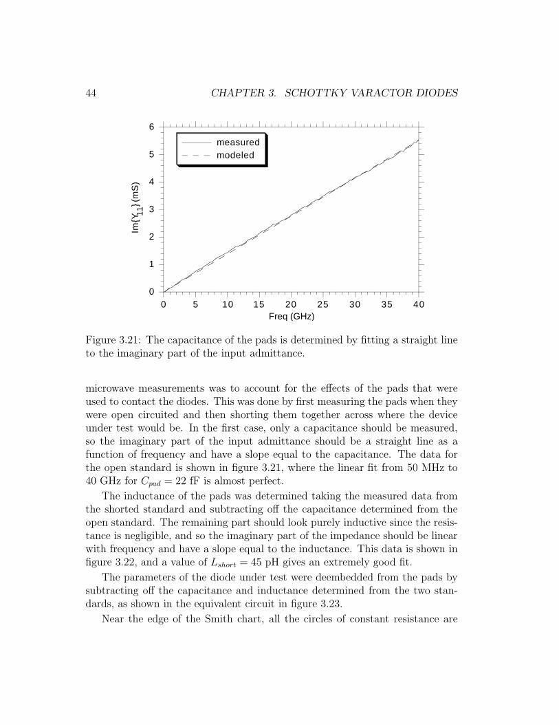
0
1
2
3
4
5
6
0
ImY
11 (
mS
)
5 10 15 20 25 30Freq (GHz)
35 40
measuredmodeled
44 CHAPTER 3. SCHOTTKY VARACTOR DIODES
Figure 3.21: The capacitance of the pads is determined by fitting a straight lineto the imaginary part of the input admittance.
microwave measurements was to account for the effects of the pads that wereused to contact the diodes. This was done by first measuring the pads when theywere open circuited and then shorting them together across where the deviceunder test would be. In the first case, only a capacitance should be measured,so the imaginary part of the input admittance should be a straight line as afunction of frequency and have a slope equal to the capacitance. The data forthe open standard is shown in figure 3.21, where the linear fit from 50 MHz to40 GHz for Cpad = 22 fF is almost perfect.
The inductance of the pads was determined taking the measured data fromthe shorted standard and subtracting off the capacitance determined from theopen standard. The remaining part should look purely inductive since the resis-tance is negligible, and so the imaginary part of the impedance should be linearwith frequency and have a slope equal to the inductance. This data is shown infigure 3.22, and a value of Lshort = 45 pH gives an extremely good fit.
The parameters of the diode under test were deembedded from the pads bysubtracting off the capacitance and inductance determined from the two stan-dards, as shown in the equivalent circuit in figure 3.23.
Near the edge of the Smith chart, all the circles of constant resistance are

0
2
4
6
8
10
12
0
ImZ
11 (
mS
)
5 10 15 20 25 30Frequency (GHz)
35 40
measuredmodeled
Cd(V ) Rs
Copen
Lshort
3.3. DIODE CHARACTERIZATION 45
Figure 3.22: The inductance of the pads is determined by fitting a straight lineto the imaginary part of the impedance after subtracting off the pad capacitance.
Figure 3.23: Circuit model used to deembed the diode under test from the pads.

S11
46 CHAPTER 3. SCHOTTKY VARACTOR DIODES
Figure 3.24: Smith Chart showing the deembedded data for a 2 µm x 42 µmdiode at 0V bias.
extremely close together, and so it is difficult to reliably identify a small Rs.This can be seen in figure 3.24 where the measured diode impedance is barelydistinguishable from the edge of the Smith Chart. This also illustrates theimportance of having an extremely good calibration.
In order to extract the small signal parameters of the diode, it was instructiveto consider the admittance of the device instead of the impedance:
Y =ω2C2Rs
1 + ω2C2R2s
+jωC
1 + ω2C2R2s
(3.16)
At frequencies ω << 1/CRs, this reduces to Y = ω2C2Rs + jωC. The capaci-tance is now readily determined because the imaginary part of the admittanceis linear with frequency and has a slope of C. The real utility in examining theadmittance instead of the impedance comes when determining Rs. The conduc-tance of the diode at frequencies well below fc is directly proportional to thediode area, so examining the real part of the admittance on a large device pro-vides for reliable extraction of Rs. Figure 3.25 shows the measured and modeledcapacitance of a 2 µm x 42 µm diode at 0 V bias. The extracted capacitance of84 fF is very close to the theoretical value of 89 fF calculated for a diode with

0
4
8
12
16
20
ImY
11 (
mS
)
0 9 18 27 36Frequency (GHz)
measuredmodeled
3.3. DIODE CHARACTERIZATION 47
Figure 3.25: Measured and modeled capacitance of a 2 µm x 42 µm diode.
N− = 1.0 · 1017 cm−3. The measurements were made on this diode because itwas the test diode that had the largest area.
By knowing the diode capacitance accurately, Rs can be determined by fittinga curve to the measured conductance, as shown in figure 3.26. The curve isparabolic with frequency, as predicted by equation 3.16, and the value ofRs = 1.2Ω determined by a least-squares fit is only 10% higher than is calculated fromthe bulk dc parameters using the equations in section 3.1. Using these measuredvalues and applying the scaling rules from section 3.1, the 1 µm diodes have alarge signal cutoff frequency of 4.1 THz.

0.0
0.1
0.2
0.3
0.4
0.5
0.6
Re
Y 11 (
mS
)
0 9 18 27 36Frequency (GHz)
measuredmodeled
48 CHAPTER 3. SCHOTTKY VARACTOR DIODES
Figure 3.26: Measured and modeled conductance of the diode, showing thequadratic frequency dependence.

Chapter 4
NLTL Characterization
After the circuits had been fabricated, a number of different measurements weremade to characterize them. The first diagnostics were on the test diodes, andthe details of these measurements were covered in the previous chapter. Thenext set of measurements was characterization of the NLTLs using a microwavenetwork analyzer. For this purpose, some of the NLTLs were not connected tosampling circuits but instead had microwave probe pads on each end. Most ofthe important parameters that characterize an NLTL can be determined fromthese measurements. The final step in the testing was to measure the two NLTLsintegrated with a sampling circuit, as diagrammed in figure 2.12.
4.1 Microwave Measurements
The first easily measured parameter is the small signal impedance of the NLTLas a function of bias. Figure 4.1 shows the measured reflection coefficient ofthe NLTL at 0 V and -6 V bias. Figure 4.2 shows that the input and outputreflection coefficients were virtually identical. The shapes of the curves is readilyunderstood. At low frequencies, where the loss of the line is small, the measuredimpedance is just the 50 Ω load transformed through the impedance of the line.As the loss increases at higher frequencies, the effect of the 50 Ω terminationis no longer seen and the measured impedance converges to the characteristicimpedance of the line. This causes the center of the circles to shift with frequency,and the high frequency loss also causes the radius of the circles to spiral inward.
These lines were designed to have Zls = 40 Ω, so the small signal designimpedances were Z(0V ) = 31 Ω and Z(−6V ) = 46 Ω. The measured valuesas determined from the curves in figures 1.1 and 1.2 were Z(0V ) = 29 Ω and
49

0V -6V
50 CHAPTER 4. NLTL CHARACTERIZATION
Figure 4.1: Measured S11 of NLTL at 0 V and -6 V bias.
Figure 4.2: The input and output impedance of the line were essentially identical.

-10
-8
-6
-4
-2
0
S21
(dB
)
0 5 10 15 20 25Frequency (GHz)
30 35 40
-6V bias
0V bias
4.1. MICROWAVE MEASUREMENTS 51
Figure 4.3: Network analyzer measurement of loss on the NLTL when biased attwo different biases.
Z(−6V ) = 39 Ω, smaller than the design values. One explanation for the lowerimpedance is that the parastic capacitances from the cell layout were loadingdown the line. With this as a premise, the calculated values of capacitancenecessary to produce the measured impedances were Cpar = 99 pF/m at 0 Vand Cpar = 89 pF/m at -6 V, a difference of only 10% at the two biases. Anestimate of 95 pF/m therefore seems reasonable.
Another parameter that is readily measured on the network analyzer is theloss of the line. Figure 4.3 shows the measured transmission through the line at0 V and -6 V. This measured S21 consists of three components: the resistive lossof the transmission line, the diode RC loss, and the impedance mismatch.
For comparison to the measured data, the NLTL loss was calculated usingequation 2.7. The transmission line’s resistance, Rl, was calculated using theskin effect approximation, and at low frequencies, where the metal is less thana skin depth thick, a modified form for the surface resistivity, Rs, was used [28]:
Rs =1
2σδ· e
h/δ − cos(h/δ) + sin(h/δ)
cosh(h/δ)− cos(h/δ)(4.1)
where σ is the conductivity of the gold, h is the thickness, and δ is the skindepth.

52 CHAPTER 4. NLTL CHARACTERIZATION
Freq Bias Measured Calculated Line Metal Diode(GHz) (V) S21 (dB) S21 (dB) Loss (dB) Loss (dB) Loss (dB)
10 0 -3.9 -4.3 3.7 3.6 0.110 -6 -2.4 -2.8 2.7 2.7 0.040 0 -9.8 -9.3 8.7 7.3 1.440 -6 -6.4 -6.3 5.6 5.4 0.2
Table 4.1: Comparison of measured and predicted values of small signal NLTLloss.
The diode loss was calculated using the values of Cd and Rs that were deter-mined from the network analyzer measurements described in section 3.3.2. Theimpedance of the line was taken from the measured data, because this has asignificant impact on the amount of loss. The impedance mismatch effect on S21
was then accounted for, and the three effects were combined to give a predictedvalue for S21. The results are summarized in table 4.1, and it can be seen thatthe predictions are in very close agreement with the measured data.
The most important parameter of an NLTL is the change in propagationdelay of a wave as the bias on the line changes from 0 V to -6 V, because it isthis difference that causes the shock wave formation. This net change in delay,or total amount of compression on the line, is how much the fall time of a signalwould be reduced if the NLTL had ideal behavior. In reality, the reduction infall time is not this large, but it is still a useful parameter to measure becauseit shows if the lines are behaving as designed. It is a way to make a linearmeasurement that characterizes the nonlinearity of the line.
Figure 4.4 shows the measured propagation delay of an NLTL when it isbiased at 0 V and -6 V. The standing wave pattern is due to the impedancemismatch of the line and becomes less severe at -6 V where the line is muchcloser to 50 Ω. The propagation delay, Td, is determined from the measuredphase of S21:
Td =dφ(S21)
dω(4.2)
The total ∆Td as measured this way is 15 ps but the design value was 20 ps, sothe line did not have the correct amount of compression. There were two likelyexplanations for this discrepancy. The first was that the diodes did not havethe right capacitance, but the measurements on both the large area and the 1µm diodes after the sidewall etch showed that the deviation from theory in the

45
50
55
60
65
70
75
80
85
Td (p
s)
0 5 10 15 20 25Frequency (GHz)
30 35 40
0 V Bias
-6 V Bias
4.1. MICROWAVE MEASUREMENTS 53
Figure 4.4: The net change in delay of the NLTL is determined by the differencein phase delay when biased at 0 V and -6 V.
C-V characteristics was too small to account for the large reduction in the linecompression.
The second possibility was that the parasitic capacitance identified from theimpedance measurements was sufficient to cause the reduction in compression. Ifa parasitic capacitance has increased the line capacitance to a significant fractionof the diode capacitance, then the change in delay with diode bias will be smaller(equation 2.1.) To account for the 25% reduction in line compression, the extracapacitance would have to be 93 pF/m, which is in extremely close agreementwith the value deduced from the impedance measurements.
The origin of this capacitance can be seen by examining the cell layout shownin figure 4.5 which shows a cell at the output end of the line that is designedto have fBr = 800 GHz. The Schottky contacts of the diodes are on either sideof the center conductor of the CPW and the ohmic contacts are embedded inthe ground planes. There is significant fringing capacitance between the padsthat connect to the Schottky fingers and the ground planes because the lateraldimensions have become so small at the output end of the line. The spacingbetween the diodes with fBr = 800 GHz is 25 µm, so in order for the line to havean average Cpar = 94 pF/mm as determined from the network analyzer data,

54 CHAPTER 4. NLTL CHARACTERIZATION
Figure 4.5: Cell layout at the output end of the NLTL where fBr = 800 GHz.The fringing capacitance becomes large because of the small lateral dimensions.
there needs only be 2.2 fF extra capacitance in this cell. This is a completelyreasonable value given the geometry of the cell.
4.2 Sampling Circuit Measurements
The circuits had been designed to be driven at 30 GHz because the high drivefrequency allows the lines to be shorter and thus have lower loss. Two differentsampling circuits were designed. The first had a differentiator circuit with around-trip time of 2 ps and the more aggressive design had only a 1 ps differen-tiator. Because the lines had less compression than designed, a drive frequencyof 40 GHz was used. It was found that the edges produced were fast enoughto strobe the samplers with the 1 ps differentiator and that the improved band-width of these samplers had an impact on the measured edge speed. Figure 4.6is a scanning electron microscope (SEM) photomicrograph showing the outputends of the two NLTLs coming in to the sampling circuit and figure 4.7 is aclose-up showing the sampling circuit. The two air bridges at the edges of thephotograph are the ones that provide the short circuit for the 1 ps differentiator.

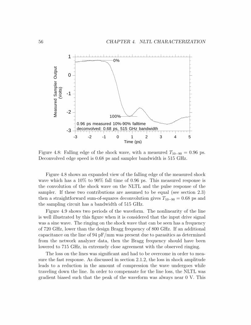
-3
-2
-1
0
1
-3 -2 -1 0
Mea
sure
d S
ampl
er O
utpu
t(V
olts
)
1 2 3 4 5
0.96 ps measured 10%-90% falltime deconvolved: 0.68 ps, 515 GHz bandwidth
0%
Time (ps)
100%
56 CHAPTER 4. NLTL CHARACTERIZATION
Figure 4.8: Falling edge of the shock wave, with a measured T10−90 = 0.96 ps.Deconvolved edge speed is 0.68 ps and sampler bandwidth is 515 GHz.
Figure 4.8 shows an expanded view of the falling edge of the measured shockwave which has a 10% to 90% fall time of 0.96 ps. This measured response isthe convolution of the shock wave on the NLTL and the pulse response of thesampler. If these two contributions are assumed to be equal (see section 2.3)then a straightforward sum-of-squares deconvolution gives T10−90 = 0.68 ps andthe sampling circuit has a bandwidth of 515 GHz.
Figure 4.9 shows two periods of the waveform. The nonlinearity of the lineis well illustrated by this figure when it is considered that the input drive signalwas a sine wave. The ringing on the shock wave that can be seen has a frequencyof 720 GHz, lower than the design Bragg frequency of 800 GHz. If an additionalcapacitance on the line of 94 pF/mm was present due to parasitics as determinedfrom the network analyzer data, then the Bragg frequency should have beenlowered to 715 GHz, in extremely close agreement with the observed ringing.
The loss on the lines was significant and had to be overcome in order to mea-sure the fast response. As discussed in section 2.1.2, the loss in shock amplitudeleads to a reduction in the amount of compression the wave undergoes whiletraveling down the line. In order to compensate for the line loss, the NLTL wasgradient biased such that the peak of the waveform was always near 0 V. This

-3
-2
-1
0
1
-25 -15 -5 5 15 25Time (ps)
Mea
sure
d S
ampl
er O
utpu
t(V
olts
)
4.3. LIMITATIONS 57
Figure 4.9: Two periods of the measured signal showing the ringing on the outputat fBr = 720 GHz.
was accomplished by bringing down a needle probe at the output end of the lineto provide a second dc bias port. Because the dc probe has a very high inductiveimpedance, it had no effect on the high frequency signal. By biasing the outputend of the line at a less negative voltage than the input, the effect of the lineloss on compression was negated. While this method was effective, it was not agood long term solution because the difference in voltage between the input andoutput forced a large current to flow down the center conductor. At the outputend of the line where the center conductor was narrow, the current level was ashigh as 1 · 106 A/cm2 which would cause electromigration problems in the Au.
4.3 Limitations
The purpose in carefully analyzing the circuits was twofold. The first was toidentify how and why the lines differed from their designed values and the secondwas to determine which parameters of the NLTL needed to be improved in orderto increase the circuit performance. The measured edge speed of 0.68 ps was invery close agreement with what had been predicted with SPICE (see figure 2.6),but it was attained under very different drive conditions than had been used in

58 CHAPTER 4. NLTL CHARACTERIZATION
the simulation.The small cells at the output end of the line contributed a number of limita-
tions to the shock line performance, especially the parasitic capacitance and loss.Referring back to figure 4.5, it can be seen that the diodes are physically as closeas they can be without having one diode interact with the one in the adjacentcell. This layout limitation put an upper limit on the Bragg frequency that couldbe attained, since fBr is inversely proportional to the diode spacing. BecausefBr was further reduced by the parasitic capacitance of the cell, it became oneof the significant limitations to the NLTL speed. The other detrimental effectsof the capacitance on the shock wave have been discussed previously.
The other major limitation of the NLTLs that produced the 0.68 ps edge wasthe loss, much of which came from the narrow transmission line at the outputend of the NLTL. One of the results of this, the loss of compression, was offsetby using the gradient biasing technique. The other problem which this did nothelp was that it made the breakdown requirements of the diodes on the line veryhigh. In order to get a 3 V step function at the output end of the line, a sinewave with a peak to peak voltage of 12 V needed to be applied at the input end.As discussed extensively in section 3.1, a large VBr requires lighter doping in theN− region of the diodes and this increases the series resistance of the diodes.If the loss on the NLTL could be reduced, the breakdown requirements for thediodes loading the line would diminish, and diodes with a higher fcls could beused (figure 3.4). This would further reduce the loss on the line and also increasethe speed of the shock edge that could be obtained, according to equation 2.3.
There was also one major limitation to the sampling circuit bandwidth, theRC rise time of the sampling diodes, as given in equation 2.10. One way thiscould be improved would be by using diodes with a lower series resistance, whichcould be done if the breakdown requirements could be reduced, as describedabove. The second way would be to make the sampling diodes smaller so thatthe capacitance of each diode would be reduced. The problem with that is that,as discussed in section 3.3.1, when the diode stripe length is less than 3 µm,the ion implantation causes significant damage to the N− region and greatlydegrades the diode’s performance. This need to reduce the area of the samplingdiodes meant that a new technique had to be developed in order to make verysmall diodes that could maintain their cutoff frequency.
Chapter 5
NLTLs With Air BridgedTransmission Lines
It was found from the analysis of the results of the NLTLs that produced the0.68 ps edge that the cell layout at the end of the lines was placing a severelimitation on the high frequency operation of the lines. The proposed solutionwas to fabricate a transmission line with the center conductor elevated abovethe substrate because this addresses the two critical problems of parasitic capac-itance and low Bragg frequency. Air bridged interconncections have often beenused in high frequency ICs to reduce the capacitive loading of the wiring, but forthe NLTL application, the technique had to be extended much further. Figure5.1 is a cross-sectional view of a coplanar line with such a geometry and showsthe contours of equipotential as determined by a quasi-static electromagneticsimulator [29].
Because the electric field lines for this structure are predominantly in air, thecapacitance per unit length of the transmission line is decreased, resulting in anincrease in velocity of the waves on the line, v = 1/
√LlineCline. With an increase
in the wave velocity, for the same physical separation between the diodes, theelectrical separation increases, increasing fBr. An additional benefit from thelower capacitance is that a wider center conductor is needed to obtain the samecharacteristic impedance, so the resistive loss goes down. Others have used thisfeature in an attempt to reduce the loss at the low frequency end of the line [30],but this effect is partly offset by the fact that the line must be longer becauseof the increased velocity. The real impact of the air lines is at the output end ofthe line where the parasitics are severe and the high Bragg frequency is needed.
With the center conductor suspended in air, it becomes possible to contact
59

60 CHAPTER 5. NLTLS WITH AIR BRIDGED TRANSMISSION LINES
Figure 5.1: Quasi-static simulation showing the lines of equipotential for a copla-nar waveguide with the center conductor elevated 3 µm above the GaAs sub-strate.
the Schottky diodes on the NLTL without touching the GaAs substrate, sothe parasitic capacitance from the diode pads will be substantially reduced.Figure 5.2 is a cross-sectional diagram of the NLTL showing how this can beaccomplished. The support for the air bridged transmission line is provided bythe Schottky diodes, and the contacts to them are made with a pad that remainsin air.
5.1 Process Development
The process was based on the electroplated air bridge process that was describedin section 3.2.6. Measurements showed that the resistivity of the plated gold wasthe same as for evaporated gold, so using the plated air bridges as the center con-ductor would not adversely affect the loss. The part of the process that neededdevelopment was a method for keeping the contacts to the diodes suspended inair. This was accomplished by using a planarizing layer of polyimide before theelectroplating process. The details of the process flow are illustrated in figure5.3. The polyimide process development relied heavily on a process flow devel-oped for ridge waveguide lasers [31] and is similar to one that is used to contactthe emitters of high speed HBTs [32].

Air BridgedCenter Conductor
Ohmic Ohmic
CPWGround
CPWGround
N- Active Layer
Semi-Insulating GaAs Substrate
N+ Layer
5.1. PROCESS DEVELOPMENT 61
Figure 5.2: The air bridged center conductor contacts the Schottky diodes with-out touching the GaAs substrate, so the parasitic pad capacitance is greatlyreduced.
After finishing the first three process steps described in section 3.2 so that theSchottky diode fabrication was complete, a 1 µm layer of polyimide was appliedto the wafer (figure 5.3 (a)). The polyimide was partially cured at a temperaturenot high enough to crosslink the polymers because the final step in the processflow was to remove the polyimide. Next, a layer of 3 µm thick photoresist wasapplied to provide a further degree of surface planarization (figure 5.3 (b)). Theselayers were then etched in an oxygen RIE system where the etch depth could bemonitored with a laser. The dielectric layers on the surface of the wafer formedan impedance match for the laser beam and so as the layers were etched, a strongstanding wave pattern was observed in the power of the reflected light. Becauseboth the refractive indices and the etch rates of the polyimide and photoresistwere almost identical, the standing wave pattern could be used to determine theamount of material that had been removed. It was found that after the lasersignal went through 22 complete cycles of the standing wave pattern, the topsof the Schottky diodes were exposed (figure 5.3 (c)).
The air bridge process was then carried out as before. After patterning thepost holes for contacting the tops of the diodes and interconnect metal, a thinflash layer of Ti/Au/Ti was sputtered (figure 5.3 (d)). The air bridges werepatterned with 3 µm thick photoresist on top of the flash layer, the first layer ofTi was etched, and the lines were electroplated (figure 5.3 (e)). The final stepsinvolved removing the photoresist and flash layers and then removing all of thepolyimide so that the electroplated lines were left suspended completely in air(figure 5.3 (f)).

(a) polyimide
(b)photoresist
(e)
air bridgephotoresist
(f)
electroplatedair bridge
(c)
exposed diodes
(d)
sputtered Ti/Au/Tipost maskphotoresist
62 CHAPTER 5. NLTLS WITH AIR BRIDGED TRANSMISSION LINES
Figure 5.3: Process flow for air bridged transmission lines.

(a)
polyimide
(b)
polyimide
5.1. PROCESS DEVELOPMENT 63
Figure 5.4: (a) When there is a small gap in a large plane of metal, the polyimidein the gap is thick, but still dips. (b) When there is a small feature in an openarea, the polyimide on top of the metal is thin.
The term “planarization” for this technique is somewhat of a misnomer. Thepolyimide conforms to the local features of the wafer in a manner that can bedescribed as a spatial low pass filter, with the polyimide following slow but notrapid variations in surface topography, and this is best understood by way ofillustration. When there is a small gap in an otherwise uninterrupted planeof metal, the polyimide is still very thick when measured from the surface ofthe wafer but will dip in the region of the gap, figure 5.4 (a). When there isa small metal feature in an otherwise vacant area, the polyimide will form abump that will be thin when measured from the top of the metal, figure 5.4(b). This geometric dependence is of utmost importance when designing thecircuit layout, because it governs which features will be exposed first when thepolyimide is etched.
It was desired to have 1 µm of polyimide left after the O2 etch, so in orderto cleanly expose the tops of the Schottky diodes, the metalization had to be≈ 1.5 µm thick. Making 1 µm features that were 1.5 µm high required a newphotolithography process because it was difficult to accurately define 1 µm linesin photoresist that is very thick. The solution was to use a surface imagingtechnique, where a thin layer of photoresist was used to define the pattern anda second layer underneath was used to give the thickness. This process flow isdiagrammed in figure 5.5. The first layer is 2 µm of SAL-PL1 [33] which is aphotoresist that is sensitive to light at the deep UV wavelength of 210 nm. TheSAL is cured at 200 C and then the second layer, a thin positive photoresist,is applied (figure 5.5 (a)). Because the SAL is cured at a high temperature andis only sensitive to deep UV light, the top layer of resist can be patterned using

photoresistSAL
photoresistSAL
SALphotoresist
(a)
(b)
(c)
64 CHAPTER 5. NLTLS WITH AIR BRIDGED TRANSMISSION LINES
Figure 5.5: (a) 2 µm of SAL-PL1 is applied and then a thin layer (< 1 µm) ofpositive photoresist. (b) The 1 µm lines are defined in the top layer of resist.(c) The SAL is flood exposed and developed to give a crisp liftoff edge.
the normal photolithography at 365 nm described in section 3.2 (figure 5.5 (b)).After completing this, the wafer is flood exposed at 210 nm and then placed inSAL developer. The flood exposure is long enough to cause some undercutting ofthe SAL layer, and so a crisp liftoff pattern is defined (figure 5.5 (c)). AppendixD contains detailed process flow sheets for both the 1 µm lithography and thepolyimide air bridge process.
5.2 Electrical Characterization
The electrical characteristics of the air bridged transmission lines were deter-mined by measuring a set of lines with a microwave network analyzer. Thebaseline designs for 75 Ω transmission lines were taken from the results of thequasi-static simulator [29] and then a set of lines was fabricated with pertur-bations around the nominal dimensions. A cross section of the air lines withthe important dimensions defined is shown in figure 5.6. The center conductor,w, was made of differing widths, 8, 12 and 16 µm, because the cell taperingdiscussed in section 2.1.2 was still applicable. The height off the substrate, h,was chosen to be 3 µm. A sensitivity analysis using the quasi-static simulatorshowed that with the center conductor this far off the substrate, the character-istics of the line would not be very sensitive to deviations in dimensions dueto processing control. Table 5.2 summarizes the measured characteristics of the

h
ws
GaAs Substrate
5.2. ELECTRICAL CHARACTERIZATION 65
Figure 5.6: Cross section of air line, showing relevant dimensions. w is the widthof the center conductor, s,, is the separation between the center conductor andground, and h is the height above the substrate. h was fixed at 3 µm and theground planes were always made 2(w + 2s).
Width Spacing Impedance Velocity Loss at 40 GHzw (µm) s (µm) Z0 (Ω) vel (108 m/s) α (dB/mm)
8 3 69 2.21 0.388 5 76 2.15 0.3312 4.5 65 2.07 0.3212 6.5 72 2.00 0.2812 8.5 76 1.94 0.2516 9 70 1.90 0.2416 11 73 1.81 0.2216 13 75 1.78 0.22
Table 5.1: Extracted parameters from network analyzer measurements of airlines, with h = 3.0µm.
lines. Both the line impedances and velocities were about 15% lower than whathad been predicted by the quasi-static simulator, which was close enough thatthe desired 75 Ω lines were within the design space covered. Note also that theloss on the lines did not decrease proportionately with increasing w because ofcurrent crowding effects along the edges of the wide center conductors.
A set of calibration standards for the line-reflect-line technique (section 3.3.2)was designed along with the transmission lines so that all of the effects of the padparasitics would be calibrated out of the measured S-parameter data. Figures5.7 and 5.8 show typical comparisons of the measured S21 data to the model fromwhich the line velocities and attenuation were extracted. Figure 5.9 compares themeasured and modeled S11 data from which the line impedance was determined.

-5
-4
-3
-2
-1
0
0 5 10
Inse
rtio
n Lo
ss (
dB)
15 20 25Frequency (GHz)
measuredmodeled
-200
-150
-100
-50
0
50
100
150
200
Pha
se o
f S21
(deg
rees
)
0 5 10 15 20 25Frequency (GHz)
measuredmodeled
66 CHAPTER 5. NLTLS WITH AIR BRIDGED TRANSMISSION LINES
Figure 5.7: Magnitude of S21 from which the loss was determined
Figure 5.8: Phase of S21 from which the velocity was determined.

-25
-20
-15
-10
-5R
efle
ctio
n C
oeffi
cien
t (d
B)
0
0 5 10 15 20Frequency (GHz)
measuredmodeled
25
5.3. SMALL DIODES 67
Figure 5.9: Magnitude of S11 from which the line impedance was determined.
5.3 Small Diodes
An additional advantage of using the air bridged transmission lines was thatit became feasible to fabricate very small diodes that did not suffer from ionimplantation damage as described in section 3.3, which was very important forincreasing the bandwidth of the sampling circuit. A top view and side view ofa 1 µm x 1 µm sampling diode are shown in figure 5.10. A very small Schottkycontact can be made in the middle of a large active region and then contactedfrom the top with an air bridge. Because the area of the diode is defined onlyby the size of the Schottky contact, the ion implantation mask can be kept wellaway from this region. This geometry has the added advantage that there issubstantial two dimensional spreading of the current in the region between theSchottky and ohmic contacts, and so the periphery-dependent terms of the seriesresistance are lower than predicted by equations (3.3-3.5). For diodes where theresistance in the N− region is small, this has a significant impact on fcls. Fordiodes with ND = 3.0 · 1017 cm−3, 1 µm x 1 µm sampling diodes had a cutofffrequency of over 10 THz.
The advantages in making a small diode also help at the output end of theNLTL. Because the velocity on the air lines is twice what it is for conventional

Air Bridged Contact
Ohmic OhmicN+ Layer
(a)
(b)
68 CHAPTER 5. NLTLS WITH AIR BRIDGED TRANSMISSION LINES
Figure 5.10: Cross section of 1 µm x 1 µm diode that can be contacted from thetop with an air bridge.
CPW on GaAs, the Bragg frequency at the output end of the line can be doubledfrom 750 to 1500 GHz, and this requires a small diode. By placing the Schottkycontacts for the diodes directly under the air bridged center conductors, smalldiodes could easily be incorporated into the NLTL. A perspective drawing ofthis is shown in figure 5.11 and an S.E.M. photomicrograph of the output endof the NLTL after fabrication is shown in figure 5.12.
5.4 NLTL Design
The air bridged transmission lines solved most of the problems that had beenidentified as limiting the performance of the 515 GHz circuits, but while theyhelped to reduce the loss, they did not eliminate it. The biggest problem re-maining, then, was the dc walkoff problem described in section 2.1.2 where thenonlinearity of the varactors is lost due to signal attenuation. This effect canbe counteracted by engineering the lines so that they have no voltage loss eventhough they have power loss. The power on a transmission line is
P =V 2
Z0
(5.1)
where V is the voltage on the line and Z0 is its characteristic impedance. Ifthe impedance at the output end of the line is larger than the impedance at the

Ohmics
Schottky
CPW Ground Plane
Air Bridged Center Conductor
5.4. NLTL DESIGN 69
Figure 5.11: Perspective drawing showing the air bridged center conductor con-tacting the top of a Schottky diode.
Figure 5.12: S.E.M. of fabricated NLTL at the high Bragg frequency end of theline.

70 CHAPTER 5. NLTLS WITH AIR BRIDGED TRANSMISSION LINES
Diode Compr Start End Start EndDoping ∆Td (ps) fBr (GHz) fBr (GHz) Zls (Ω) Zls (Ω)
1e17 20 260 1500 20 441e17 25 260 1500 20 473e17 20 260 1500 20 443e17 25 260 1500 20 47
Table 5.2: Important design parameters for the air bridged NLTLs withimpedance tapering.
input end by the ratio of the powers,
ZoutZin
=PinPout
(5.2)
then the voltage at the two ends of the line will be the same.Others have used impedance tapering on NLTLs to match them to a low
impedance driver source [34], but for this work the large signal impedance ofthe lines was tapered to exactly compensate for the power loss on the line sothat a large voltage swing would be maintained down the whole line. Becauseeach section of the NLTL was designed to have a higher Bragg frequency andlarger Zls than the preceding section, there was no closed-form expression fordetermining the parameters of each section of the NLTLs. To design the lines,a computer program was written where the starting Bragg frequency, the end-ing Bragg frequency, the number of line sections and the starting Zls were allspecified. The parameters for the NLTL were generated by determining the firstsection of the line, calculating its loss, increasing Zls proportionately for the nextsection, increasing fBr and then designing that section of the line. This was doneiteratively and the propagation delay for each section was summed. The speci-fied number of sections for the line had to be varied until the desired amount ofcompression for the entire line was obtained. The computer program that wasused can be found in Appendix E along with the output files that included theline parameters, a SPICE file and a layout file. Table 5.2 summarizes the lineparameters of four different lines that were designed.
The impedance tapering was based on the calculated loss at 40 GHz becauseit is the voltage swing at the fundamental frequency that is driving the diodes.Overcompensating for the loss at the drive frequency would be counterproductivebecause the diodes would be driven into reverse breakdown. The loss at higher

10-5
10-4
0.001
0.01
0.1
1
10 100 1000
Loss
(dB
)Diode LossSkin Effect Loss
Frequency (GHz)
5.5. NETWORK ANALYZER DATA ON NLTLS 71
Figure 5.13: Loss mechanisms on a unit cell at the output end of the line, showingthat the diode loss becomes dominant above 100 GHz.
frequencies cannot be offset; it can only be minimized. One of the deficiencies ofSPICE is that it cannot model the frequency dependent skin effect loss on thetransmission lines. To model the loss at the fundamental frequency, a lumpedresistor was added after each section of transmission line that was equal to thecalculated resistance at 40 GHz. Figure 5.13 shows the diode loss and the skineffect loss of the last cell of the NLTL. Because the skin effect loss is ∝
√f and
the diode loss is∝ f2, above 100 GHz the diode RC loss becomes dominant. Thisis accounted for in the SPICE simulation, so all the important loss phenomenonare being modeled.
5.5 Network Analyzer Data on NLTLs
As discussed previously, network analyzer data on test lines provides the mostvaluable insight to the operation of the lines, so after fabricating the new lineson diodes with ND = 1 · 1017 cm−3, the same set of data was taken as before.Figure 5.14 shows the measured Td for the line at 0 V and -6 V bias. Thisline was designed to have 20 ps of compression and this is almost exactly whatthe microwave data shows. This indicates that the air lines were successful

30
40
50
60
70
80
0 5
Td (p
s)
10 15 20 25 30 35Frequency (GHz)
40
0 V Bias
-6 V Bias
72 CHAPTER 5. NLTLS WITH AIR BRIDGED TRANSMISSION LINES
Figure 5.14: Network analyzer data showing the measured delay of an NLTLwhen biased at 0 V and -6 V.
in eliminating the parasitic capacitance that had caused a 25% reduction incompression on the earlier generation of NLTLs. Lines designed to have 25 psof compression also had measured delays equal to the design value.
Figure 5.15 shows the measured S11 and S22 of the line, and it is readilyapparent that the impedances at the input and output ends of the line aredifferent. For comparison, figure 5.16 shows the same impedance measurementsfor one of the previous generation of lines where Zls was constant along the line.Because of the impedance tapering, it was not possible to extract an exact valuefor the input and output impedance, but the apparent values were close enoughto the design values to believe that the lines were behaving as intended.
5.6 Measured Sampling Circuit Results
The sampling circuits were designed with two different sizes of diodes: 1.5 µmx 1.5 µm and 1.0 µm x 1.0 µm using the technique described in section 5.3.The reason for using the larger diodes for some of the samplers was in case theprocessing yield on the 1.0 µm x 1.0 µm was low. This did not turn out to bea problem, so the only advantage of having the larger diodes was to compare

S11
S22
5.6. MEASURED SAMPLING CIRCUIT RESULTS 73
Figure 5.15: Measured input and output impedance of an NLTL designed witha tapered Zls.
Figure 5.16: Measured input and output impedance of an NLTL from an earlierdesign where Zls was constant.

74 CHAPTER 5. NLTLS WITH AIR BRIDGED TRANSMISSION LINES
Figure 5.17: S.E.M. image of the sampling circuits with 1.0 µm x 1.0 µm diodescontacted by air bridges. The distance between the diodes and the differentiatorair bridge is only 0.6 ps round trip.
the effect of sampling circuit bandwidth on the measured edge speed. For bothtypes of samplers, the differentiator was designed to have a round trip time of0.6 ps, which was as short as could be comfortably incorporated into the layout.Figure 5.17 shows an S.E.M. of the sampling circuit. The sampling diodes arenot visible, but the air bridges contacting them can be seen in the middle of thephotograph. The extremely short distance between the sampling diodes and thedifferentiator air bridge is very evident.
The measured waveform from a line with 1.0 µm x 1.0 µm sampling diodesand 20 ps of compression is shown in figure 5.18 and has a 10% to 90% falltime of 0.68 ps. If the same assumption was made as before that the NLTLand sampling circuit were providing equal contributions to the measured signal,then the sampling circuit has a deconvolved bandwidth of 725 GHz. However,the sampling circuit bandwidth did not appear to be limiting the measuredperformance. The same edge speed was measured with sampling circuits havingboth 1.0 µm x 1.0 µm diodes and 1.5 µm x 1.5 µm diodes. Since this changes theRC rise time of the sampling circuit by more than a factor of 2, this indicates thatthis was not the limiting time constant in the circuit. Edge speeds measured withthe older style sampler, with 1.0 µm x 3.0 µm diodes and a 1.0 ps differentiator,were substantially slower with T10−90 of 0.92 ps. The new sampling circuits wereimproved enough to apparently have no impact on the measured shock wave.

-4.0
-3.0
-2.0
-1.0
0.0
1.0M
easu
red
Sam
pler
Out
put
(Vol
ts)
-1.5 -1.0 -0.5 0.0 0.5 1.0 1.5
0%
100%
Time (ps)
3.7 Volt step with0.68 ps measured10%-90% falltime;725 GHz deconvolved sampler bandwidth
5.7. LIMITATIONS 75
Figure 5.18: Measured waveform with a 10% to 90% fall time of 0.68 ps. Assum-ing equal contributions of the NLTL and sampler, the sampling circuits have adeconvolved bandwidth of 725 GHz.
The other significant feature of the measurements to discuss is the effect ofthe impedance tapering. The measured edge has a peak-to-peak voltage 3.7V, which is 35% larger than was measured on the previous generation of lines.Even more importantly, attempts to improve the circuit performance by usinggradient biasing were futile, so the problem with dc walkoff had been solved.Also, the 20 ps lines gave slightly faster edges than the 25 ps lines. The loss ofthe 25 ps lines was enough larger that the impedance tapering was not enoughto completely compensate for the power loss and this affected the performanceof the line.
5.7 Limitations
All of the measurements indicated that the air bridged transmission lines hadsolved the problems identified from the previous generation of circuits. Theselines had the right amount of compression, the sampling circuits with 1.0 µm x1.0 µm diodes were substantially faster, there clearly was no Bragg ringing onthe waveform in figure 5.18, and gradient dc biasing was no longer necessary.

76 CHAPTER 5. NLTLS WITH AIR BRIDGED TRANSMISSION LINES
The measured edge speed, however, was slower than any of the time constantsin the circuit would predict. This is attributed to a velocity saturation effect onthe depletion edge movement at the output end of the line.
From the measured voltage swing of the shock wave, it was calculated thatthe depletion edge of the diodes at the output end of the line moved 145 nm in the0.68 ps 10% to 9 % fall time, giving it an average velocity of 2.1·107 cm/sec, whichis the typical maximum velocity for electrons in GaAs. Normally depletion edgemovement is considered to be an event that occurs within a dielectric relaxationtime, but this is only true when it is a small signal phenomenon. In the caseof the NLTL, where large voltage swings are present, the edge of the depletionregion has to physically move the entire 145 nm, and so the small signal analysisis no longer valid.
This velocity saturation problem has also been encountered by people workingwith high frequency varactor multipliers [35]. In these studies, it was found thatthe measured power and efficiency of the multipliers under high drive powerswere significantly smaller than had been predicted even though the predictionswere reasonably accurate at lower drive powers. Careful calculations showed thatthe power began to saturate at drive levels where the depletion edge movementexceeded about 2 · 107 cm/sec. In follow up work, varactor diodes were designedspecifically to address this problem by increasing the doping levels, and the resultwas an increase in output power of 300% for the same size device [36].
The solution to this problem in the context of NLTLs is the same: to usediodes with heavier doping. The distance the depletion edge moves is inverselyproportional to the doping (equation 2.1), so by increasing the doping level from1 to 3 · 1017 cm−3, for the same voltage swing the depletion edge only has tomove
√3 as far. It was in anticipation of this problem that on the same mask
set lines were designed with both levels of diode doping. The experiments withthe initial process run on the heavier doped diodes did not lead to conclusiveresults. The 1 µm diodes had anomalously high capacitance per unit area, andsince the sampling diodes would have
√3 more capacitance any way, it appeared
that the measurements were sampler limited. Attempts are being made to finda way to simultaneously have fast diodes at the output end of the line and stillhave low capacitance sampling diodes. This will be the focus of the work thatcarries on from this thesis project.

Chapter 6
Future Development of NLTLs
In order to get beyond 725 GHz, the diode design tradeoffs have become morecomplicated. On the NLTL, increasing the doping in the N- region leads toan increase in speed because the shock wave fall time is limited by the RCproduct (equation 2.3) and the resistance of the diode decreases faster than thecapacitance increases. The situation is not the same in the sampling circuit.Each sampling diode is effectively loaded by a 50 Ω termination and so when thediode resistance becomes small compared to 50 Ω, reducing Rs further has littleeffect. This means that as the doping in the diode is increased, the samplingcircuit charging time is increasing as Cd·50 Ω and the sampling circuit bandwidthbegins to decrease with increasing diode doping.
This was apparently the problem with the first attempt to make the circuitswith diodes doped at N− = 3.0 · 1017 cm−3. With only
√3 more capacitance,
this was not expected to be a problem yet, but because the diode capacitanceper unit area was anomalously high, it was enough to slow down the sampler.This conclusion that the speed was sampler limited was corroborated by the factthat the signals measured with the 1 µm x 1 µm diodes were faster than thosemeasured by the 1.5 µm x 1.5 µm diodes.
The proposed solution was to have two different types of diodes on the line:one that was lightly doped in the sampling region and another that was dopedwith N− = 3.0 · 1017 cm−3 on the rest of the line. To make things even better,a hyperabrupt doping profile was used for the lightly doped layer, allowing forthree different diodes to be used in the circuit, as shown in figure 6.1. At theinput end of the line, the hyperabrupt doping profile gives 14 V breakdown anda 4:1 change in capacitance at the expense of diode cutoff frequency. This layerwas then etched off at the output end of the line where the fast diodes were
77

0 100
1 1017
2 1017
3 1017
4 1017
5 1017
0 200
Dop
ing
(cm
-3)
400 600 800 1000
Output
Sampler
BuriedN+ Layer
Depth (nm)
78 CHAPTER 6. FUTURE DEVELOPMENT OF NLTLS
Figure 6.1: Three step doping profile used in an attempt to make faster samplers.At the input end of the line, the hyperabrupt diodes have a large breakdownvoltage and strong nonlinearity at the expense cutoff frequency. At the outputend of the line the breakdown is lower but the diodes are extremely fast. Thesampling diodes are designed to have as small a capacitance as possible.
needed. The velocity saturation limit of these diodes is 0.39 ps (0.68 ps/√
3),which is the edge speed predicted by the SPICE simulation that includes all theother effects. To make the sampling diodes, the hyperabrupt layer was etcheddown until only 150 nm of extremely lightly doped material was left, giving thema very small capacitance and a smaller rise time of only 120 fs.
The measured waveform from these circuits is shown in figure 6.2 and hasan extremely slow fall time of 1.6 ps. At this point, the circuits should not bediode limited on either the NLTL or the sampling circuit and so there mustbe something more fundamental wrong with them. There was a very stronginterference signal on which the sampled waveform was superimposed, and theoutputs from the two sampling diodes were significantly different. The conclusionfrom this is that the sampling circuit layout needs to be changed in order tosuppress the interference signal and achieve a better balance between the twosampling diodes. It is not understood at this time why this problem wasn’t assevere with the more lightly doped diodes that produced the 725 GHz result.

-6.0
-4.0
-2.0
0.0
2.0
-3
Vo
ltag
e
-2 -1 0 1 2 3 4 5Time (ps)
6.1. REACHING 2 THZ BANDWIDTH 79
Figure 6.2: Measured waveform from the three step wafer showing a very slowedge speed of 1.6 ps.
6.1 Reaching 2 THz Bandwidth
If the problems with the sampling circuit layout can be easily fixed, then theapproach for pushing the technology to 2 THz would follow almost the exactsame route as the path from 500 GHz to 1 THz. The requirements are: (1) asmaller RC time constant for the diodes at the output end of the line; (2) ashorter depletion edge movement for these diodes; (3) a higher Bragg frequencyat the output end; and (4) smaller sampling diodes.
Solutions to the last two are the easiest because they do not require anyepitaxial doping profile design or any new technology development. To increasethe Bragg frequency, the air bridged coplanar waveguide technology can readilybe extended to making air microstrip lines. By connecting the two CPW groundplanes together underneath the center conductor, the line becomes microstripwith all field lines in air and so the velocity must be 3·108 m/s, 50% higher thanfor the CPW lines. With the diode spacing at the end of the line reduced to 18µm, fBr=2800 GHz.
The area of the sampling diodes can be reduced by going to electron beamlithography. Using the technology developed for the submicron Schottky collec-

80 CHAPTER 6. FUTURE DEVELOPMENT OF NLTLS
tors discussed in the next chapter, sampling diodes can be defined that are assmall as 0.25 µm x 1.0 µm. The E-beam lithography will also help with theBragg frequency issue. One of the limits to how closely packed the diodes canbe is the alignment tolerances that required for contact lithography. By using E-beam written diodes at the output end of the line, the registration error betweenthe Schottky fingers and ohmic pads becomes negligible. Reducing the diodespacing to 18 µm from 25 µm then creates no problems at all. Also, becausethe transmission line is completely shielded from the semiconductor, there is noneed to worry about an ion implantation mask in this region, and so anotheralignment tolerance is eliminated.
6.2 Diode Design
Addressing the first two issues is much more difficult because the constraintson the diode have become much more severe. The tradeoff between speed andbreakdown has become unmanageable. A two step doping profile will be required:one at the input end of the line that has sufficient breakdown and a second one atthe output end of the line that meets the speed requirements. The best solutionwould be to use one of the 725 GHz lines discussed in the previous chapter asa driver for a high speed output stage. With a 0.68 ps, 4 V incident edge, theoutput stage would not need much compression nor have to sustain very largevoltages.
Because these proposed strategies are essentially technology that has alreadybeen demonstrated for this thesis project, almost the entire burden falls on thehigh speed diode design. A simple calculation sets the starting point for thedesign. A 2 THz shock wave has a 10% to 90% fall time of 175 fs, 3.9 timesfaster than the measured 0.68 ps edge. Assuming velocity saturation, the dopinghas to be increased by the square of this, so the N− doping would have to become1.6 · 1018 cm−3. The activation of dopants at this high a doping level becomesquite variable, and so a different approach is required.
The solution proposed here is to use a delta-doped diode where a sheet of Sidopants is deposited at the plane at which the 0 bias depletion depth is desired,making this distance insensitive to the other doping parameters. If the saturationvelocity remains at 2·107 cm/sec, the depletion edge can only move 30 nm in160 fs. The best compromise for the diode design is to have this result in a 2:1capacitance change instead of the 3:1 used previously. Because the amount ofcompression needed in the output section of line will be small, it is preferable totrade speed for nonlinearity in the diode.

1017
1018
1019
0 20 40 60
Dop
ing
(cm
-3)
80 100
Buried N+ Layer
deltadoping
Depth (nm)
6.2. DIODE DESIGN 81
Figure 6.3: Doping profile of proposed diode which has Cjo=3.8 fF and Rs = 5Ω · µm2
The proposed doping profile is shown in figure 6.3. The surface is doped withN = 3.0 · 1017 cm−3 because the breakdown properties of this material were wellcharacterized during this thesis work. Next comes a sheet of donors at 30 nmwith σ = 3.5 · 1012 cm−2, a value within the range of what is commonly usedfor delta-doped HEMTs. The next layer is again 30 nm thick, which defines thedepletion edge movement, and is doped N = 6.0 · 1017 cm−3. Figure 6.4 showsthe electric field profile of the diode at the punch through voltage of 2.9 V. Themaximum electric field at this point is 8.7 · 105 V/cm, which is the measuredbreakdown field of the diodes doped with N = 3.0 · 1017 cm−3.
Once again, the tradeoff between R and C that was discussed in chapter 2is no longer valid because the capacitance is being determined independentlyfrom the doping level by the placement of the delta doping. The E- beam diodesprovide the solution to the problem. The thin heavily doped region reduces thevertical resistance in the diode to 1 Ω ·µm2, so the resistance becomes dominatedby the periphery dependent terms. By scaling the diode to 0.25 µm width andreducing the Schottky to ohmic separation to 1.0 µm, the total resistance ofthe diode becomes 5 Ω · µm2. Figure 6.5 shows a SPICE simulation using thisdiode. With a 4 V, 1 ps input step, a 170 fs shock wave is generated, meeting

0
2
4
6
8
10
0
|E| (
105 V
/cm
)
20 40 60 80 100Depth (nm)
82 CHAPTER 6. FUTURE DEVELOPMENT OF NLTLS
Figure 6.4: E-field profile of the proposed diodes at the punch-through voltage.
the design goal of 2 THz. A sampling circuit with 0.25 µm x 1.0 µm diodes onthis material will have an RC time constant of 120 fs. The narrow depletionregion is important for the sampling diodes as well or else their response timewould also become transit time limited at these very high speeds.
The one problem with the proposed design is how to integrate it into a two-step doping profile. The delta-doped diode must be on the bottom becauseany series resistance from a diode underneath it would ruin any of its speedadvantages. This means that the top layer must be etched off at the outputend of the line and in the sampling circuit. The technological challenge here isthat 200 to 300 nm of material must be etched off and then the etch has to stopvery precisely in order to define the 30 nm 0-bias depletion depth for the burieddiode. This should be manageable with a slow H3PO4 based etch that etches at50 nm/min, but it is not trivial. A dry etch is not workable because without aheterojunction there is no way to use a laser to monitor the etch depth.
6.3 Conclusion
There is still some work to be done to push the sampling circuit bandwidth to1 THz, but if these problems, which are believed to be relatively minor, can be

-3.5
-3
-2.5
-2
-1.5
-1
-0.5
0
0.5
Sim
ulat
ed S
hock
Wav
e (V
)
0.0 0.5 1.0 1.5 2.0Time (ps)
Simulated 10% to 90%fall time=170 fs
6.3. CONCLUSION 83
Figure 6.5: SPICE simulation of 170 fs shock wave using the proposed diode.The line is designed assuming air microstrip transmission lines, fBr=2800 GHz,and ∆Td=0.8 ps. The input signal is a 3 V, 0.8 ps step function.

84 CHAPTER 6. FUTURE DEVELOPMENT OF NLTLS
worked out, then the path to 2 THz is straightforward. By going to E-beamsampling diodes and air microstrip lines, only the varactor diode performanceremains as a limit. It is possible that at time scales < 200 fs and distances <300 A, there will be significant deviations in device performance from what hasbeen already observed, so the diode design may not have to be as aggressive asthe one proposed. The project becomes one that is primarily an exploration ofhigh frequency device physics and should be both interesting to the researcherand valuable to the scientific community.

Chapter 7
Schottky-Collector ResonantTunneling Diodes
Resonant tunneling diodes (RTDs) are of interest because they have a region ofnegative differential resistance that can be used in circuits to generate oscillationsat frequencies well above the operating range of transistors. In the AlAs/GaAssystem, oscillation have been reported at frequencies as high as 420 GHz [37].In the InAs/AlSb system, waveguide oscillators have been operated as high as712 GHz [38].
In this work a new type of RTD, the Schottky-collector resonant tunnelingdiode (SRTD) was investigated. The idea behind this device was that by replac-ing the conventional ohmic contacted collector with a Schottky contact, all of theadvantages of device scaling that had been studied for the varactor diodes couldnow be applied to the RTD. SRTDs with 0.1 µm wide Schottky collectors similarto those used for T-gate HEMTS [39] were fabricated in the AlAs/GaAs system.From their measured dc and microwave parameters a maximum frequency ofoscillation, fmax, of 900 GHz was calculated, at least twice as high as for anypreviously reported RTD in this material. By applying the Schottky collectortechnique to RTDs in the material system of AlAs/InGaAs latticed matched toInP, an fmax greater than 2 THz is expected.
7.1 Theory of RTD Operation
The conduction band diagram of an RTD is shown in figure 7.1. The quantumwell region is formed with two layers of a wide bandgap material, typically AlAs,on either side of a well that is usually 40 to 60 A wide. The shaded region in
85

Space-chargeLayer
E
JTunnelling
EC
EFCollector
Emitter
86 CHAPTER 7. SCHOTTKY-COLLECTOR RTDS
Figure 7.1: Conduction band diagram of an RTD under forward bias. Theshaded region represents the quasi-bound state in the quantum well. The energydistribution of the electrons in the emitter is also indicated.
the quantum well in the figure represents the energy level of the quasi-boundstate in the well. On one side of the quantum well is an undoped space-chargeregion which the electrons transit under high electric field. On the other sideof the quantum well is the emitter which provides the source of electrons forthe tunneling process. The curve above the emitter in the figure represents theenergy distribution of the electrons.
As indicated in the diagram, a forward voltage is applied to the diode tocreate an electric field across the quantum well and space-charge regions. Asthe energy level of the qausi- bound state in the well is lowered with respect tothe electrons in the emitter, an increasing number of electrons are available toparticipate in the tunneling process and the current through the diode increases.This continues until the electric field across the diode is such that the energy levelof the bound state coincides with the energy level at which the peak in the emitterelectron distribution occurs. Beyond that point, a fewer number of electrons areavailable to tunnel and the current actually decreases for increasing voltage. Thisis the phenomenon that gives rise to the region of negative differential resistance.Beyond a certain level, the barriers become low enough that there is a substantialamount of thermionic emission over them and the current again begins to risewith a continued increase in the voltage (figure 7.2).
The important points of the curve are the peak current, Ip, the voltage atwhich this occurs, Vp, the minimum, or valley, current, Iv, and the valley voltage,Vv. One of the parameters that is used to characterize an RTD is the peak tovalley ratio (PV R) of the current, Ip/Iv. The other key parameter is the negativeconductance, Gn of the diode. For calculating the diode’s fmax, the small signalGn is used, and this is taken to be the maximum of the slope in the negative

Iv
I p
7.1. THEORY OF RTD OPERATION 87
Figure 7.2: I-V curve of a typical RTD. The peak current, Ip, occurs at a voltageVp and the minimum current, Iv, occurs at the valley voltage, Vv.
differential resistance (NDR) region. A large signal negative conductance canalso be defined as the average negative conductance over the entire NDR region:
−Gnls =Ip − IvVp − Vv
(7.1)
In designing the quantum well structure, there is usually a direct tradeoff be-tween the two parameters Ip and PV R, and these both impact Gn. For example,increasing the doping level in the emitter increases the peak current density, butbecause there are more electrons at the higher energies, the thermionic emissionover the barriers becomes significant at lower biases and the valley current isnot as low, so the PV R is reduced. The same tradeoff occurs if the barriers aremade thinner. In a quantum well with thin barriers, the energy band for thequasi-bound state broadens so more electrons can take place in the tunnelingprocess. This leads to an increase in the peak current density, but also reducesthe sharpness of the resonance, and so again the PV R is reduced.
There are different design strategies for different applications. When theRTD is going to be used for switching applications such as in a logic circuit, itis important to have the valley current be as small as possible [40], so the PV Ris of primary importance here. For sub-millimeter wave oscillators the designemphasis is different. For this application another important parameter is theavailable current Ip − Iv because this is directly related to the power availablefrom the diode when it is oscillating in the NDR region. In terms of availablecurrent, there are diminishing returns for increasing the PV R. With a PV Rof 2, half of the peak current is available in the NDR region, and with a PV R

Schottky and interconnect metal
N+ buried layer, N+ top contact layerohmic metalsemi-insulating GaAs
N+ emitter layerquantum well
88 CHAPTER 7. SCHOTTKY-COLLECTOR RTDS
Figure 7.3: Cross-sectional views comparing the structures of (a) the conven-tional RTD; and (b) the Schottky-collector RTD.
of 5, this increases to 80%. Increasing the PV R from 5 to ∞ will only resultin an increase of 20% in available current. It is much more advantageous toincrease the peak current at the expense of the PV R. In fact, for the very thinbarriers that are desirable for high frequency oscillators (see section 7.2), thepeak current increases more rapidly than the PV R degrades, so both Gn andthe available current are increased by thinning the barriers.
Figure 7.3 shows cross-sectional diagrams that compare the structures of theconventional RTD and the Schottky-collector RTD. For the conventional device,two ohmic contacts are made in parallel to the heavily doped buried N+ layer.On top of this layer is grown the emitter, which is typically doped at aboutND = 1 · 1018 cm−3 and governs the electron flux across the quantum well. Nextis grown a thin spacer layer, followed by the quantum well structure. After thiscomes the undoped space- charge region and then another heavily doped N+layer to which the top ohmic contact is made. The structure for the SRTD issimilar except the top N+ layer and ohmic contact are eliminated and insteada Schottky contact is made directly to the space-charge region.
To see how this eliminates the resistance at the collector contact it is in-structive to compare the band diagrams of the two devices (figure 7.4). Electrontransport through the quantum well region and space-charge layer is identical inthe two devices, with equal currents transported for equal electric fields acrossthe well and space-charge layer. After crossing the space-charge layer, electronsare collected by an N+ layer in the conventional RTD and must then cross theresistive top ohmic contact. In the SRTD, after crossing the space-charge re-gion, the electrons drop over the potential step qφb at the metal semiconductorinterface. The top ohmic contact resistance is eliminated at the expense of anadditional voltage drop equal to the height of the potential drop, which is 0.8 V

Schottky metal
q b
ohmicmetal
N+collector layer
space-charge layer
well
N+emitter layer space-
charge layer
well
N+emitter layer
(a) (b)
7.1. THEORY OF RTD OPERATION 89
Figure 7.4: Band diagrams for (a) a conventional RTD and (b) a Schottky-collector RTD.
for GaAs.
It is important to understand that the SRTD is not the same as a conventionalRTD in series with a Schottky diode. This is best illustrated by again comparingthe band diagram of the SRTD (figure 7.4 (b)) to that of the standard Schottkydiode (figure 7.5). In a Schottky diode, the height of the potential barrier seenby the electrons in the semiconductor is governed by the applied forward bias,Vf . Because of the Fermi-Dirac distribution of electrons, there is an exponentialdependence of current on applied voltage:
If ∼= Iss exp(qVfkT
)(7.2)
From this the familiar expression for the small signal junction impedance, rjunct,is derived:
rjunct =dVfdIf
=kT
qIf(7.3)
In the Schottky-collector RTD under forward bias, there is no potential barrierto the electrons at the metal semiconductor interface. Because φb is independentof the current flow under normal operating conditions, dφb/dI = 0 and so theSchottky contact has added no differential impedance to the RTD.
The only possible detrimental effect that the Schottky contact could havewould be if there were significant quantum mechanical reflection of the electronsat the interface because of the large change in potential and effective mass.If the probability of reflection at the interface is p, then the round trip timeacross the space-charge region would be increased by a factor on the order of(1 + p)/(1 − p). If p were large, this could increase the transit time enough toimpact the frequency response of the device.

space-chargelayer
Schottkymetal
N+emitterlayer
q b
q( ms Vf)qVf
90 CHAPTER 7. SCHOTTKY-COLLECTOR RTDS
Figure 7.5: Band diagram of a conventional Schottky diode.
To quantify this effect, the reflection probability at the interface was calcu-lated using the following assumptions. Parabolic bands in the semiconductorand monocrystalline metal were assumed so that a standard effective mass ap-proximation could be made for the electrons [41]. A potential step of 1.4 eV wasused because the effective mass approximation requires that the energy differ-ence used in the calculation be the energy between the bottoms of the conductionbands and the 0.8 eV Schottky barrier height is between the GaAs conductionband and the Fermi level in the metal, not the conduction band. Assuming theelectrons lose a minimal amount of energy while crossing the 350 A space-chargelayer, the reflection probability is only 3%. Even if the incident electron energyis as low as 0.1 eV above the conduction band, the reflection probability remainsless than 13%. This estimate is in line with measurements on Schottky mixerswith cutoff frequencies as high as 25 THz [14]. The incident electron energyin these devices are generally much lower than in the SRTD and the measuredresults are not consistent with large contributions from reflections.
7.2 Increasing RTD Bandwidth
The benefits of the Schottky collector towards improving fmax of the RTD canbe understood by examining the small signal equivalent circuit model of an RTDwhen biased in the NDR region (figure 7.6). It consists of the extrinsic parasiticseries resistance, Rs, the parallel plate capacitance from the undoped space-charge region, C, the effective negative resistance of the diode, Rn = 1/Gn, andan inductance associated with the quantum well, Lqw, that accounts for the timerequired for an electron to tunnel through the double barrier structure.

Rs
Lqw
C
Rn
7.2. INCREASING RTD BANDWIDTH 91
Figure 7.6: Small signal equivalent circuit model of an RTD when biased in thenegative differential resistance region.
If Lqw is neglected, there is a simple expression for fmax of the RTD:
fmax =1
2πRnC
√|Rn| −Rs
Rs
(7.4)
In order to make fmax high, the 1/RnC product should be maximized. Thisis done by designing the quantum well region to give the device a large peak-to-valley ratio and as high a current density as possible, limited by thermalconstraints. Changing the width of the space-charge layer has little impact onthis. The capacitance changes linearly with the width, but because the currentthrough the diode is a function of the electric field across the space-charge layer,the voltage required to attain Ip and Iv also changes linearly with the width,and so the RnC product is independent of this dimension.
Having adjusted the quantum well design accordingly, fmax is then limitedby the series resistance. The purpose of the Schottky collector is to make thisas small as possible. Replacing the collector ohmic with a Schottky contacteliminates that resistance, but the more beneficial result is that the Schottkycontact can be scaled to submicron dimensions to further reduce the remainingcomponents of the parasitic resistance. This is almost identical to the scalingeffects that were described for the Schottky varactor diode in section 3.1, andthe reason for this can be seen by examining figure 7.7, which is a cross-sectionaldiagram of the SRTD showing the various components of the parasitics.
The capacitance is not voltage dependent as it is for the varactor diode but isinstead fixed by the width of the undoped region between the Schottky contactand the emitter layer: C = εWL/d where d is the sum of the thicknesses ofthe space-charge region and double barrier quantum well. When d becomes anappreciable fraction of W , there will be signifcant lateral extent of the electricfield under the Schottky contact, and it becomes more appropriate to analyzethe diode in terms of an effective contact width, Weff = W + 2d.

Semi-insulating Substrate
Rspr 2Rbl2Rbl
2Roc 2Roc
D DW
Ohmic OhmicRe
L
92 CHAPTER 7. SCHOTTKY-COLLECTOR RTDS
Figure 7.7: Cross-sectional diagram of an SRTD showing the components of theparasitics, almost identical to those of a Schottky varactor.
The vertical resistance through the emitter layer, Re, has the same functionalform as the resistance through the undepleted N− region of the varactor. Forthe RTD, the doping in this region is chosen to determine the electron flux acrossthe quantum well, but it can made extremely thin to keep Re small:
Re =ρeTeWeffL
(7.5)
The next two components of the series resistance are identical to those dis-cussed in section 3.1:
Rbl =1
2· DL· ρN+
TN+
(7.6)
Roc =1
2L
√ρcont ·
ρN+
TN+
(7.7)
There is also a spreading resistance in the SRTD that accounts for the currentspreading out in the buried N+ layer, and when the Schottky contact width isreduced to submicron dimensions, the current flow in this region is very twodimensional. In this case, the spreading resistance can be approximated as
Rspr =ρN+
πL· ln
(TN+
Weff
)(7.8)
For submicron Schottky collectors, there will be an additional resistance andinductance along the collector finger, analogous to the gate resistance and in-ductance in an FET. To minimize these parasitics, a T-gate structure was used

0
400
800
1200
1600
Max
imum
Fre
quen
cy
of O
scill
atio
n (G
Hz)
2000
0.1 1.0Collector Width (µm)
ConventionalSchottky
10.0
7.2. INCREASING RTD BANDWIDTH 93
Figure 7.8: Dependence of fmax on collector contact width for the conventionalRTD (dashed line) and Schottky-collector RTD (solid line), when τqw is ne-glected.
to increase the cross-sectional area of the collector finger, and it will be shownlater that these terms had negligible impact on the fmax of the RTD’s.
Because Rspr, Rbl and Roc are inversely proportional to L, and C and Rn areproportional to W · L, decreasing W and increasing L to maintain a constantdiode area greatly reduces Rs and results in a substantial increase in fmax. Thisis illustrated in figure 7.8 which uses equation 7.4 to show how fmax increases asthe Schottky contact width is decreased. For the conventional ohmic-contacteddevice, there is little improvement in the frequency response as W is reducedbelow about 1 µm because the resistance becomes dominated by the top ohmiccontact, which is an area term. However, for the SRTD, the dominant resistancesare all periphery dependent terms, so as the diode’s periphery-to-area ratio isincreased, fmax continues to increase.
When Rs ¿ Rn, the transit time across the quantum well, τqw, can no longerbe neglected. To leading order, the effect of the transit time delay on the current-voltage relation for the RTD can be described by the differnetial equation:
i(t) + τqw∂i(t)
∂t= − 1
Rn
v(t) (7.9)

10-4
10-3
10-2
Tra
nsm
isio
n C
oeff
icie
nt 10-1
100
0.00 0.05Incident Energy (eV)
0.10 0.15 0.20 0.25
17 A Barrier11 A Barrier
94 CHAPTER 7. SCHOTTKY-COLLECTOR RTDS
Figure 7.9: Transmission probability of electrons through a double barrier struc-ture compared for two different barrier widths.
This is the equation of a series RL network where R = −Rn and L = −τqwRn
and thus the quantum well inductance is defined to be Lqw = −τqwRn (negativein the NDR region). When this model was first proposed, a series of experimentswas performed on RTDs intentionally designed to have very large values of Lqwand the measured results confirmed the validity of the model [42]. Theoreticalcalculations of this lifetime show that it decreases exponentially as the barrierregions are thinned [43]. The explanation for this is that the tunneling timefor an electron to get either in or out of the bound state in the well is givenby the uncertainty relation τ = h/∆E where ∆E is the width in energy of thetransmission probability. As the barriers are made thinner, the energy band overwhich tunneling occurs broadens, ∆E increases, and τqw = 2h/∆E decreases.
Figure 7.9 compares the transmission probability as a function of energy forquantum wells with two different barrier thicknesses. These calculations wereperformed at the flat band condition for quantum wells having a 45 A GaAs wellbounded by AlAs barriers of either 17 A or 11 A. For the thinner barriers, theresonant peak is wider and less sharp. This translates to a shorter well lifetime,higher current density and a lower PVR.
SRTDs with various AlAs barrier thicknesses were fabricated. Table 7.2 sum-
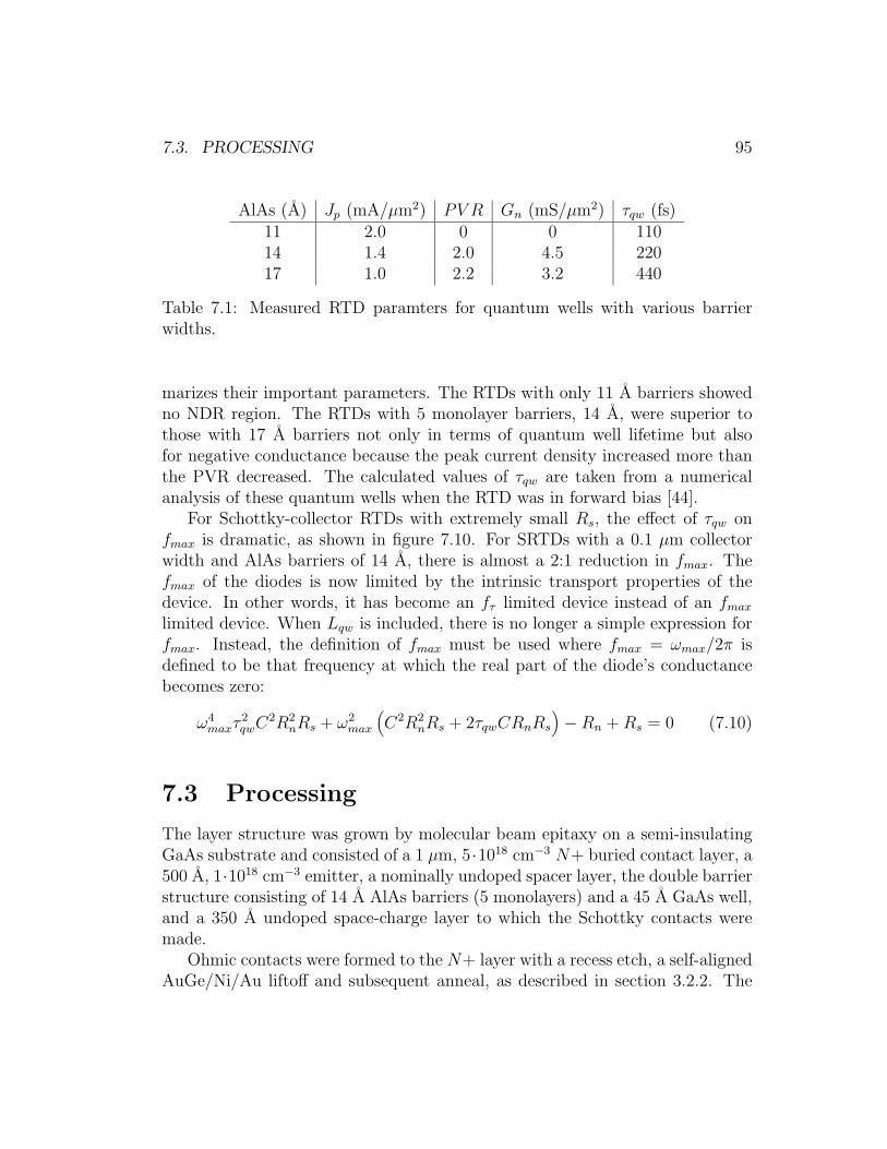
7.3. PROCESSING 95
AlAs (A) Jp (mA/µm2) PV R Gn (mS/µm2) τqw (fs)11 2.0 0 0 11014 1.4 2.0 4.5 22017 1.0 2.2 3.2 440
Table 7.1: Measured RTD paramters for quantum wells with various barrierwidths.
marizes their important parameters. The RTDs with only 11 A barriers showedno NDR region. The RTDs with 5 monolayer barriers, 14 A, were superior tothose with 17 A barriers not only in terms of quantum well lifetime but alsofor negative conductance because the peak current density increased more thanthe PVR decreased. The calculated values of τqw are taken from a numericalanalysis of these quantum wells when the RTD was in forward bias [44].
For Schottky-collector RTDs with extremely small Rs, the effect of τqw onfmax is dramatic, as shown in figure 7.10. For SRTDs with a 0.1 µm collectorwidth and AlAs barriers of 14 A, there is almost a 2:1 reduction in fmax. Thefmax of the diodes is now limited by the intrinsic transport properties of thedevice. In other words, it has become an fτ limited device instead of an fmaxlimited device. When Lqw is included, there is no longer a simple expression forfmax. Instead, the definition of fmax must be used where fmax = ωmax/2π isdefined to be that frequency at which the real part of the diode’s conductancebecomes zero:
ω4maxτ
2qwC
2R2nRs + ω2
max
(C2R2
nRs + 2τqwCRnRs
)−Rn +Rs = 0 (7.10)
7.3 Processing
The layer structure was grown by molecular beam epitaxy on a semi-insulatingGaAs substrate and consisted of a 1 µm, 5 ·1018 cm−3 N+ buried contact layer, a500 A, 1·1018 cm−3 emitter, a nominally undoped spacer layer, the double barrierstructure consisting of 14 A AlAs barriers (5 monolayers) and a 45 A GaAs well,and a 350 A undoped space-charge layer to which the Schottky contacts weremade.
Ohmic contacts were formed to the N+ layer with a recess etch, a self-alignedAuGe/Ni/Au liftoff and subsequent anneal, as described in section 3.2.2. The

0
400
800
1200
1600
2000M
axim
um F
requ
ency
of O
scill
atio
n (G
Hz)
0.1 1.0 10.0Schottky Collector Width (µm)
Simple modelComplete model
96 CHAPTER 7. SCHOTTKY-COLLECTOR RTDS
Figure 7.10: Comparison of fmax for SRTDs with and without the effect of thequantum well lifetime.
0.1 µm Schottky collectors were defined using an electron beam T-gate processdeveloped for HEMTs at the Jet Propulsion Laboratory. The trilayer resistconsisted of 496 K molecular weight PMMA diluted to 2.5% concentration, aPMMA/PMAA 9% copolymer, and a top layer of very dilute 2300 K PMMA.The collector process also incorporated air bridges fabricated by using a lowenough dose of electrons in these regions to avoid exposing the base PMMAlayer [45], which meant that the active area of the diodes was defined by theactual contact area of the 0.1 µm footprint, not by the size of the etched mesas(figure 7.11). The air bridged part of the E-beam finger was flared out in orderto minimize the series resistance and inductance along it.
The devices were mesa isolated using a wet H3PO4:H2O2 etch and were etchedlong enough so that the E-beam air bridges were undercut completely. Half ofthe devices were then passivated with 1200 A of SiN in an electron-cyclotronresonance system at 160 C. Ti/Pt/Au interconnect metal was deposited, andcontacts to the tops of the mesas were formed with electroplated air bridges usingthe process described in section 3.2.6. An S.E.M. photograph of a multi-fingerSRTD is shown in figure 7.12.

S.I. Substrate
Active Mesa Mesa
Air bridged electron beam finger 0.1 µm
footprint
Electroplated air bridge
7.3. PROCESSING 97
Figure 7.11: Side view of SRTD. The active area of the diode is defined by the0.1 µm footprint of the E-beam finger. The top of the collector finger is used toair bridge to a second mesa to provide isolation.
Figure 7.12: S.E.M. of a completed SRTD. Each of the 6 fingers has a 0.1 µm x20 µm footprint.

Commercial Bias Tee 45 MHz to 60 GHz
50
10 nF1 µF470 µF
DCBias
10 50
Voltage Sense
98 CHAPTER 7. SCHOTTKY-COLLECTOR RTDS
Figure 7.13: Biasing network used to stabilize RTDs.
7.4 Measured Results
The devices were laid out with 50 Ω coplanar waveguide feed structures so thatconventional microwave probes could be used for testing. With the use of a biastee network that presented the RTDs with a 50 Ω source impedance over atleast the dc to 60 GHz bandwidth (figure 7.13), diodes with areas ≤ 1.0 µm2
were stable even when biased in the NDR region, so accurate dc and microwavemeasurements could be made. Because the RTDs form a parallel resonant circuitwith the admittance of the bias source, as long as the source conductance of 17to 20 mS was greater than the negative conductance of the RTD, the systemshould have been stable. However, because the RTDs had an fmax much higherthan the bandwidth of the bias network, it was found that only diodes withGn < 7 mS could be successfully stabilized because above 60 GHz the RTDswere not presented with a well-controlled bias admittance. The dc I-V curve ofa stabilized 1.0 µm2 SRTD is shown in figure 7.14. The passivated diodes had a1.4 · 105 A/cm2 peak current density, assuming a 0.2 µm collector width, a 2.0:1PVR and -4.5 mS/µm2 peak negative conductance.
Because of the lateral fringing of the electric field under the Schottky contact,the effective width of it was greater than had been lithographically defined. Bycomparing the capacitance of large area diodes to that of unpassivated diodeswith 0.1 µm E-beam fingers, an effective collector width of 0.20 µm was de-termined. Passivated diodes had a capacitance of 2.8 fF/µm2, including theadditional parasitics of the SiN layer. The capacitance of the 0.1 µm SRTDswas determined using a microwave network analyzer (NWA). The calibrationand deembedding was done using the techniques discussed in section 3.3.2. The
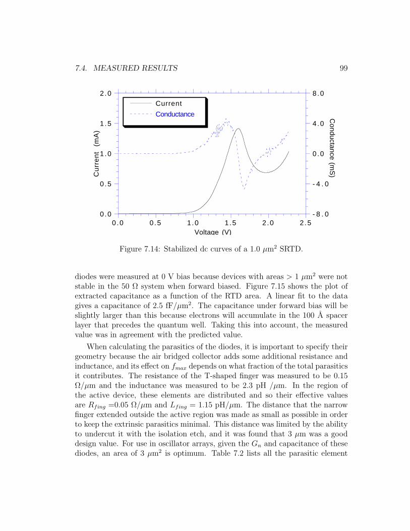
0.0
0 .5
1 .0
1 .5
2 .0C
urr
en
t (m
A)
Conductance (m
S)
- 8 . 0
- 4 . 0
0 .0
4 .0
8 .0
0 .0 0 .5 1 .0 1 .5 2 .0Voltage (V)
Current
Conductance
2.5
7.4. MEASURED RESULTS 99
Figure 7.14: Stabilized dc curves of a 1.0 µm2 SRTD.
diodes were measured at 0 V bias because devices with areas > 1 µm2 were notstable in the 50 Ω system when forward biased. Figure 7.15 shows the plot ofextracted capacitance as a function of the RTD area. A linear fit to the datagives a capacitance of 2.5 fF/µm2. The capacitance under forward bias will beslightly larger than this because electrons will accumulate in the 100 A spacerlayer that precedes the quantum well. Taking this into account, the measuredvalue was in agreement with the predicted value.
When calculating the parasitics of the diodes, it is important to specify theirgeometry because the air bridged collector adds some additional resistance andinductance, and its effect on fmax depends on what fraction of the total parasiticsit contributes. The resistance of the T-shaped finger was measured to be 0.15Ω/µm and the inductance was measured to be 2.3 pH /µm. In the region ofthe active device, these elements are distributed and so their effective valuesare Rfing =0.05 Ω/µm and Lfing = 1.15 pH/µm. The distance that the narrowfinger extended outside the active region was made as small as possible in orderto keep the extrinsic parasitics minimal. This distance was limited by the abilityto undercut it with the isolation etch, and it was found that 3 µm was a gooddesign value. For use in oscillator arrays, given the Gn and capacitance of thesediodes, an area of 3 µm2 is optimum. Table 7.2 lists all the parasitic element

0
10
20
30
40
50
60
70
80C
apac
itanc
e (f
F)
0 5 10 15 20 25 30 35 40RTD Area (µm2)
100 CHAPTER 7. SCHOTTKY-COLLECTOR RTDS
Figure 7.15: Measured SRTD capacitance at 0 V bias as a function of diodearea.
values for a diode of this size assuming that is designed with two collector fingerseach 7.5 µm long. Using τqw = 220 fs, an fmax of 900 GHz is computed.
Microwave measurements with the RTDs in forward bias were also made onthe small devices that could be stabilized. The difficulty in this measurement wasthat very small signal power levels were needed. As can be seen from figure 7.2,the negative conductance curve is very steep, and so it is important to be makinga truly small signal measurement in order to accurately measure Gn. This provedto be problematic on the NWA. Figure 7.16 shows the NWA power output asa function of frequency. The frequencies from 20 to 40 GHz are generated byusing a doubler, and because of the gain slope in the system, in order to havesufficient power at 40 GHz the power at 20 GHz is 10 dB higher. This jump inpower at 20 GHz was enough to drive the RTDs into large signal operation, andso there was a step in the measured value of Gn between 19.9 and 20.0 GHz.
This problem was circumvented by making the measurements with two dif-ferent calibrations: the first from 0.1 to 19.9 GHz and the second from 20.1to 40 GHz. The network analyzer has a power slope compensation capability,so the power output could be leveled for the upper frequency band. The twodifferent calibrations could be stored and then instantaneously recalled, so the

-30
-25
-20
-15
-10
-5
0
0 5
Pow
er O
utpu
t (d
Bm
)
10 15 20 25 30 35 40Frequency (GHz)
7.4. MEASURED RESULTS 101
Component ValueRoc 0.63 ΩRbl 0.46 ΩRspr 0.23 ΩRe 0.33 ΩRfing 0.19 ΩRext 0.30 ΩLfing 4.3 pHLext 4.6 pH
Table 7.2: Parasitics of a 3 µm2 SRTD designed with two collector fingers each7.5 µm long.
Figure 7.16: Power output of network analyzer. There is a 10 dB jump in powerat 20 GHz in order to drive the frequency doubler.

-2.0
-1.6
-1.2
-0.8
-0.4
0.0
0.0 10.0 20.0
Rea
lY11
(m
S)
30.0 40.0
MeasuredModeled
Frequency (GHz)
102 CHAPTER 7. SCHOTTKY-COLLECTOR RTDS
Figure 7.17: Network analyzer data showing the flat negative conductance to 40GHz. The ripples are attributed to variations in signal power.
RTDs could be biased up and then measured sequentially over the two differentfrequency ranges. The measured data is shown in figure 7.17.
The negative conductance has some bumps in it due to the imperfect cor-rection for the NWA’s output power, but the curve is essentially flat to 40 GHzand Gn is in agreement with the measured dc value. Because the rolloff of theG(ω) is to second and fourth order in frequency (equation 7.10), measurementsto only a small fraction of the device’s bandwidth do not permit an extrapo-lation to fmax as is usually done for transistors which have an fmax curve thatrolls off predictably at 6 dB/octave. Given existing instrument limitations, fmaxcan be experimentally verified only by building oscillators and testing them atsub-mm-wave frequencies. Oscillators up to 500 GHz have been designed withthese devices and are presently awaiting fabrication.

Chapter 8
Conclusion
By improving each of the individual components that are integrated to forman NLTL and sampler, the circuit bandwidth was increased by a factor of 3 to725 GHz. The 1 µm 4 THz Schottky diodes were the first step towards thatend and improved circuit performance to 500 GHz. By using the air bridgedtransmission line to reduce loss, eliminate pad parasitics and increase the Braggfrequency the circuit bandwidth was pushed up to 725 GHz. These circuits area solid technology that can incorporated into a new generation of measurementinstruments. They no longer require a gradient dc biasing scheme and they donot have to be driven to the limits of diode breakdown to produce subpicosecondedges, so they are well-suited for system level applications.
The network analyzers require two sampling circuits on each channel in orderto separate incident and reflected waves [9], so some layout modifications wouldbe required, but even with the increased complexity, the sampler bandwidthshould remain above 600 GHz. The 3.7 V step functions generated by the NLTLsare sufficiently large to strobe both of the samplers. By using this technology, thebandwidth limits as the system level work is pushed towards the sub-millimeter-wave range will not come from the sampling circuits.
8.1 Air Bridged Transmission Lines
The air bridged transmission lines have already been incorporated into other de-signs. The first application where these were required was a multiplexer circuitfor 100 Gb/sec data transmission that was based primarily on an earlier genera-tion of NLTLs. A simplified schematic diagram of the four diode sampling bridgeis shown in figure 8.1. The design constraints on such a bridge are more severe
103

Input Output
+ Strobe
- Strobe
4 Diode Bridge
104 CHAPTER 8. CONCLUSION
Figure 8.1: Schematic diagram of a four diode bridge designed for 100 Gb/secswitching.
than on the simpler two diode bridge. First of all, the diodes need to be smallerbecause there are now twice as many that have to be charged by the strobepulses. Secondly, in order to have good isolation between the input and outputwhen the bridge is turned off, the diodes need to be small so that the capacitivecoupling through them is small. To meet these requirements the diodes in thebridge needed to be 1.5 µm x 1.5 µm, and the only way to successfully makethese is to make small dots and contact them from the top with a suspended airbridge.
The other circuit that has been designed with the air coplanar waveguide is atraveling wave amplifier (TWA) based on 0.1 µm AlInAs/InGaAs/InP HEMTS[1] that has 200 GHz bandwidth. A schematic diagram of a TWA is shown infigure 8.2. The basic design principle of a TWA is very similar to the NLTLin that the gate and drain capacitances of the transistors are incorporated intosynthetic transmission lines designed to have a loaded impedance of 50 Ω. Theselines also have a Bragg frequency, and without using the air lines to increase thewave velocity, it would have been physically impossible to reach 200 GHz becausethe transistors would have been overlapping.
These two examples illustrate the versatility of the air bridged transmissionlines. While they were developed specifically for the nonlinear transmissionline application, they address issues that are of concern in most high frequencycircuits. The air lines are an enabling technology that will find many applicationsas integrated circuits push into the millimeter and sub-millimeter wave ranges.

Output
Input
ZO
ZO
8.2. FUTURE DEVELOPMENT OF SRTDS 105
Figure 8.2: Schematic diagram of a traveling wave amplifier. The design principleis similar to an NLTL in that synthetic transmission lines are formed using thegate and drain capacitances of the transistors.
8.2 Future Development of Schottky-Collector
RTDs
The 900 GHz RTDs fabricated as part of this thesis work are the first steptowards the long range goal of building solid state oscillators that produce milli-watts of power at 1 THz. In order to accomplish this goal, there are a number ofimportant advances that still need to be made. The first is to apply the Schot-tky collector concept to RTDs made with AlAs/InGaAs quantum wells latticematched to InP. RTDs in this material system have higher peak current densi-ties and higher peak-to-valley ratios [46] and hence more negative conductance.The quantum well lifetime is also about a factor of 2 lower than for compara-ble structures in AlAs/GaAs, so 0.1 µm SRTDs fabricated with AlAs/InGaAsshould have fmax > 2 THz. The power out of an RTD oscillator is proportionalto 1 − (f/fmax)
2, so reasonable amounts of power are still available at fmax/2,which means that a 2 THz device should be adequate for a 1 THz oscillator.
The second component that needs to be developed is a stabilizing elementthat can be integrated with the SRTDs on wafer. For measuring discrete devices,an external 50 Ω bias network was a simple solution but is unacceptable for usewith sub-mm- wave oscillators. The dc stability of the RTDs also puts a sizeconstraint on them. In order to be stable in a 50 Ω system, |Gn| < 20 mS, whichlimits the area of the diode and, hence, the power. In order to get appreciableamounts of power, an array of antenna coupled RTDs will be necessary.
Building dense oscillator arrays at frequencies above 500 GHz may requirethe use of the air bridged transmission line technology developed for the NLTLs.

106 CHAPTER 8. CONCLUSION
In many simple oscillators, the resonant element in the network is a quarter waveopen circuited transmission line. Because a quarter wave length at 1 THz onGaAs is only 28 µm, doubling the wave velocity using the air lines is probablya requirement for this type of oscillator topology. Another benefit of the airline technology is the ability to contact very small diodes without adding anyparasitics. In order to have a very small, very clean layout at 1 THz, it may benecessary to adapt this to the RTDs. This is another potential applications forthe air lines illustrate the fact that the technology is not limited to the NLTLsfor which it was developed but that it addresses the problems encountered in avariety of sub-mm-wave integrated circuits.

Appendix A
Design Files for SubpicosecondShock Lines
Following are the programs that were used to design the shock lines describedin detail in chapter 4. Section A.1 contains the c program that was used togenerate the SPICE file and the layout file that was readable by an Academymacro. Section A.2 contains the listing of the SPICE file. Section A.3 containsthe data for the layout file that is readable by an Academy macro program.
A.1 C Program for File Generation
#include <stdio.h>
#include <ctype.h>
#include <string.h>
#include <math.h>
#define PI 3.141592654 /* pi */
#define V 113.3893419 /* Velocity in GaAs um/ps */
/* This program generates a Spice file and a layout file */
/* It creates both ground plane diode cells */
/* and center conductor diode cells */
/* Modified 8/26/92 by Scott Allen */
main()
int n,i,w,l,lastw;
107

108APPENDIX A. DESIGN FILES FOR SUBPICOSECOND SHOCK LINES
float fb0,fbx,zls,zl,tcomp,rs,cjo,phi,m,iss,in,floss;
float vmax,vmin,cmax,cmin,qmax,qmin,cls,t0,tx,a0,cr;
float tline,k,lline,x,y,z,lng,area,sq,fb,lngb,atten,lam;
char a[128],b[128],fsim[64],flay[64],t[1];
FILE *fs,*fl;
/***********************************************************************
*/
/* Introduction */
/***********************************************************************
*/
printf("This program will generate NLTLs for you.\n");
printf("You can either do a homogeneous line, or an\n");
printf("inhomogeneous line. The difference is that\n");
printf("you enter either starting and ending bragg\n");
printf("frequencies (which determine the number of\n");
printf("sections and the tapering rule), or define\n");
printf("the number of sections and the tapering rule\n");
printf("(tapering rule = 1 for homogeneous line).\n");
printf("This programme uses a 6th order polynomial cap.\n\n");
printf("Please enter starting Bragg frequency (GHz) : ");
scanf("%s",a);
fb0=atof(a);
printf("Please enter ending Bragg frequency (GHz) : ");
scanf("%s",a);
fbx=atof(a);
printf("Please enter line compression (ps) : ");
scanf("%s",a);
tcomp=atof(a);
printf("Please enter large signal impedance (ohms) : ");
scanf("%s",a);
zls=atof(a);
printf("Please enter line impedance (ohms) : ");
scanf("%s",a);
zl=atof(a);
/***********************************************************************
*/

A.1. C PROGRAM FOR FILE GENERATION 109
/* Get the diode data */
/***********************************************************************
*/
/* Diode Parameters (1X1 diode) (ff, ohms) */
printf("\nDefault Diode Parameters: (1 um X 1 um)\n");
rs=29.26;
cjo=1.84;
phi=0.80;
m=0.50;
iss=1;
in=1.2;
printf("Series resistance: RS = %f ohm X um^2\n",rs);
printf("Zero-bias capacitance: CJ0 = %f fF / um^2\n",cjo);
printf("Barrier potential: PHI = %f V\n",phi);
printf("Grading constant: M = %f\n",m);
printf("Saturation current: ISS = %f pA / um^2\n",iss);
printf("Ideality factor: N = %f\n",in);
printf("\nDo you want to change them?");
scanf("%s",a);
if (a[0] == ’y’)
printf("Please enter RS = ");
scanf("%s",a);
rs=atof(a);
printf("Please enter CJO = ");
scanf("%s",a);
cjo=atof(a);
printf("Please enter PHI = ");
scanf("%s",a);
phi=atof(a);
printf("Please enter M = ");
scanf("%s",a);
m=atof(a);
printf("Please enter ISS = ");
scanf("%s",a);
iss=atof(a);
printf("Please enter N = ");

110APPENDIX A. DESIGN FILES FOR SUBPICOSECOND SHOCK LINES
scanf("%s",a);
in=atof(a);
printf("\nPlease enter maximum then minimum voltage:\n");
printf("(reverse bias max then min e.g. 6 then 0.\n");
scanf("%s",a);
vmax=atof(a);
scanf("%s",a);
vmin=atof(a);
cmin=cjo/exp(m*log(1+vmax/phi));
cmax=cjo/exp(m*log(1+vmin/phi));
qmin=phi*cjo*exp((1-m)*log(1+vmin/phi))/(1-m);
qmax=phi*cjo*exp((1-m)*log(1+vmax/phi))/(1-m);
cls=(qmax-qmin)/(vmax-vmin);
t0=(1000*zls)/(PI*fb0*zl);
tx=(1000*zls)/(PI*fbx*zl);
a0=(zl/zls)*(zl/zls)-1;
cr=sqrt(a0)*(sqrt(1/a0+cmax/cls)-sqrt(1/a0+cmin/cls));
tline=tcomp/cr;
if(fbx != fb0)
k=(tline-t0)/(tline-tx);
n=(0.5+log(tx/t0)/log(k));
lline=V*((t0-k*tx)/(1-k));
else
k=1;
n=0.5+tline/t0;
lline=V*n*t0;
printf("\nThe line has the following parameters:\n\n");
printf("Large Signal Capacitance : %f ff/um^2\n",cls);
printf("Compression ratio : %f\n",cr);

A.1. C PROGRAM FOR FILE GENERATION 111
printf("Tapering factor : %f\n",k);
printf("Number of sections : %d\n",n);
printf("Total line length : %f um\n\n",lline);
printf("Please enter circuit file name: ");
scanf("%s",fsim);
strcpy(flay,fsim);
strcat(fsim,"_sim.ckt");
strcat(flay,"_lay.ckt");
printf("\nThere will be two files: *_sim.ckt and *_lay.ckt\n");
fs=fopen(fsim,"w");
fl=fopen(flay,"w");
printf("\nDo you want to include tranmission line loss?");
scanf("%s",a);
floss=10;
if (a[0] == ’y’)
printf("\nEnter skin loss frequency (GHz) : ");
scanf("%s",b);
floss=atof(b);
/* Write the files */
fprintf(fs,"! SPICE file for NLTL with %.2f GHz initial Bragg frequency,\n",fb0);
fprintf(fs,"! %.2f GHz final Bragg frequency and %f tapering rule,\n",fbx,k);
fprintf(fs,"! and %.2f ps total compression.\n",tcomp);
fprintf(fs,"DIM\n");
fprintf(fs," LNG UM\n");
fprintf(fs,"CKT\n");
fprintf(fl,"! Academy file for NLTL with %.2f GHz initial Bragg
frequency,\n",fb0);
fprintf(fl,"! %.2f GHz final Bragg frequency and %f tapering rule,\n",fbx,k);
fprintf(fl,"! and %.2f ps total compression.\n",tcomp);
fprintf(fl,"DIM\n");
fprintf(fl," LNG UM\n");
fprintf(fl,"CKT\n");
/* initialize lastw to max width */

112APPENDIX A. DESIGN FILES FOR SUBPICOSECOND SHOCK LINES
lastw=14;
x=((0.5*exp(zl/11.33893419)-1)/(0.5*exp(zl/11.33893419)+1));
y=x*x*x*x;
z=(1-sqrt(1-y))/(2*sqrt(1-y));
for(i=1;i<n+2;i++)
lng=V*t0*exp((i-1)*log(k));
lngb=lng*(1+k)/2;
area=1e6*((1-(zls/zl)*(zls/zl))/(PI*fb0*zls))*exp((i-1)*log(k))/cls;
w=1+200/(1+2*z);
/* Determine aspect ratio, type and design rule */
while (lng < w*(1.5*(1+z*2)))
w--;
if (w < 3)
w=3;
if (area > 24.5)
l=2;
lam=3;
if (w == lastw )
strcpy(t,"A");
else
strcpy(t,"D");
else if (area > 7.5)
l=1;
lam=3;
if (w == lastw )
strcpy(t,"A");
else
strcpy(t,"D");

A.1. C PROGRAM FOR FILE GENERATION 113
else if (area > 5.75)
w=2;
l=1;
lam=2;
strcpy(t,"C");
else
w=1;
l=1;
lam=2;
strcpy(t,"C");
sq += lng/w;
lastw =w;
fb=fb0*exp((1-i)*log(k));
if (a[0] == ’n’)
atten=0;
else
atten=8.685889638*sqrt(floss*PI*1e9*2.44e-8*4*PI*1e-
7)/(2*zls*w);
fprintf(fl," NLTL%s_U%d %d %d Z=%.2f W=%d ADI=%.2f
LLI=%.2f LAM=%.1f LAMS=%d LAMO=2 !
fb=%.2f\n",t,i,i,i+1,zl,w,area,lng,lam,l,fb);
if(i==1)
fprintf(fs," TLINP_T0 201 1 Z=%.2f L=%.2f K=7 A=%e
F=%f\n",zl,lng/2,atten,floss);
fprintf(fs," S1PA_D%d %d 0 [MODEL=MIKE%d AREA=%.2f] !
fb=%.2f\n",i,i,l,area,fb);
if(i==n+1)
fprintf(fs," TLINP_T%d %d %d Z=%.2f L=%.2f K=7 A=%e
F=%f\n",i,i,i+1,zl,lng/2,atten,floss);
else
114APPENDIX A. DESIGN FILES FOR SUBPICOSECOND SHOCK LINES
fprintf(fs," TLINP_T%d %d %d Z=%.2f L=%.2f K=7 A=%e
F=%f\n",i,i,i+1,zl,lngb,atten,floss);
fprintf(fl," DEF2P 1 %d NLTL%d\n",i,i-1);
fprintf(fl,"! Total number of squares is %.2f\n",sq);
fprintf(fs," DEF2P 201 %d NLTL\n",i);
fprintf(fs,"! Total number of squares is %.2f\n",sq);
fprintf(fs,"MODEL\n");
fprintf(fs," MIKE D RS=%f CJO=%fE-15 VJ=%f &\n",rs,cjo,phi);
fprintf(fs," M=%f IS=%fE-12 N=%f\n",m,iss,in);
fprintf(fs,"SOURCE\n");
fprintf(fs," NLTL RES_RIN 201 202 R=50\n");
fprintf(fs," NLTL IVS_VIN 202 0 TRAN=SIN(-6 14 9E9 0 0 90)\n");
fprintf(fs," NLTL RES_RL %d 0 R=50\n",i);
fprintf(fs,"CONTROL\n");
fprintf(fs," NLTL TRAN 10E-12 2E-9\n");
fprintf(fs,"SPICEOUT\n");
fprintf(fs," NLTL TRAN V(ALL)\n");
fclose(fs);
fclose(fl);
printf("Do you want to do it again? ");
scanf("%s",t);
if (t[0]==’n’ || t[0]==’N’)
exit(0);
main();
A.2 SPICE File
! SPICE file for NLTL with 125.00 GHz initial Bragg frequency,
! 800.00 GHz final Bragg frequency and 0.984789 tapering rule,
! and 60.00 ps total compression.
DIM
LNG UM
CKT

A.2. SPICE FILE 115
TLINP_T0 201 1 Z=75.00 L=77.00 K=7 A=0.000000e+00 F=10.000000
S1PA_D1 1 0 [MODEL=MIKE2 AREA=48.47] ! fb=125.00
TLINP_T1 1 2 Z=75.00 L=152.83 K=7 A=0.000000e+00 F=10.000000
S1PA_D2 2 0 [MODEL=MIKE2 AREA=47.73] ! fb=126.93
TLINP_T2 2 3 Z=75.00 L=150.50 K=7 A=0.000000e+00 F=10.000000
S1PA_D3 3 0 [MODEL=MIKE2 AREA=47.01] ! fb=128.89
TLINP_T3 3 4 Z=75.00 L=148.21 K=7 A=0.000000e+00 F=10.000000
S1PA_D4 4 0 [MODEL=MIKE2 AREA=46.29] ! fb=130.88
TLINP_T4 4 5 Z=75.00 L=145.96 K=7 A=0.000000e+00 F=10.000000
S1PA_D5 5 0 [MODEL=MIKE2 AREA=45.59] ! fb=132.90
TLINP_T5 5 6 Z=75.00 L=143.74 K=7 A=0.000000e+00 F=10.000000
S1PA_D6 6 0 [MODEL=MIKE2 AREA=44.89] ! fb=134.96
TLINP_T6 6 7 Z=75.00 L=141.55 K=7 A=0.000000e+00 F=10.000000
S1PA_D7 7 0 [MODEL=MIKE2 AREA=44.21] ! fb=137.04
TLINP_T7 7 8 Z=75.00 L=139.40 K=7 A=0.000000e+00 F=10.000000
S1PA_D8 8 0 [MODEL=MIKE2 AREA=43.54] ! fb=139.16
TLINP_T8 8 9 Z=75.00 L=137.28 K=7 A=0.000000e+00 F=10.000000
S1PA_D9 9 0 [MODEL=MIKE2 AREA=42.88] ! fb=141.31
TLINP_T9 9 10 Z=75.00 L=135.19 K=7 A=0.000000e+00 F=10.000000
S1PA_D10 10 0 [MODEL=MIKE2 AREA=42.22] ! fb=143.49
TLINP_T10 10 11 Z=75.00 L=133.13 K=7 A=0.000000e+00 F=10.000000
S1PA_D11 11 0 [MODEL=MIKE2 AREA=41.58] ! fb=145.71
TLINP_T11 11 12 Z=75.00 L=131.11 K=7 A=0.000000e+00 F=10.000000
S1PA_D12 12 0 [MODEL=MIKE2 AREA=40.95] ! fb=147.96
TLINP_T12 12 13 Z=75.00 L=129.11 K=7 A=0.000000e+00 F=10.000000
S1PA_D13 13 0 [MODEL=MIKE2 AREA=40.33] ! fb=150.24
TLINP_T13 13 14 Z=75.00 L=127.15 K=7 A=0.000000e+00 F=10.000000
S1PA_D14 14 0 [MODEL=MIKE2 AREA=39.71] ! fb=152.56
TLINP_T14 14 15 Z=75.00 L=125.21 K=7 A=0.000000e+00 F=10.000000
S1PA_D15 15 0 [MODEL=MIKE2 AREA=39.11] ! fb=154.92
TLINP_T15 15 16 Z=75.00 L=123.31 K=7 A=0.000000e+00 F=10.000000
S1PA_D16 16 0 [MODEL=MIKE2 AREA=38.51] ! fb=157.31
TLINP_T16 16 17 Z=75.00 L=121.43 K=7 A=0.000000e+00 F=10.000000
S1PA_D17 17 0 [MODEL=MIKE2 AREA=37.93] ! fb=159.74
TLINP_T17 17 18 Z=75.00 L=119.59 K=7 A=0.000000e+00 F=10.000000
S1PA_D18 18 0 [MODEL=MIKE2 AREA=37.35] ! fb=162.21
TLINP_T18 18 19 Z=75.00 L=117.77 K=7 A=0.000000e+00 F=10.000000
S1PA_D19 19 0 [MODEL=MIKE2 AREA=36.78] ! fb=164.72
116APPENDIX A. DESIGN FILES FOR SUBPICOSECOND SHOCK LINES
TLINP_T19 19 20 Z=75.00 L=115.98 K=7 A=0.000000e+00 F=10.000000
S1PA_D20 20 0 [MODEL=MIKE2 AREA=36.22] ! fb=167.26
TLINP_T20 20 21 Z=75.00 L=114.21 K=7 A=0.000000e+00 F=10.000000
S1PA_D21 21 0 [MODEL=MIKE2 AREA=35.67] ! fb=169.84
TLINP_T21 21 22 Z=75.00 L=112.47 K=7 A=0.000000e+00 F=10.000000
S1PA_D22 22 0 [MODEL=MIKE2 AREA=35.13] ! fb=172.47
TLINP_T22 22 23 Z=75.00 L=110.76 K=7 A=0.000000e+00 F=10.000000
S1PA_D23 23 0 [MODEL=MIKE2 AREA=34.59] ! fb=175.13
TLINP_T23 23 24 Z=75.00 L=109.08 K=7 A=0.000000e+00 F=10.000000
S1PA_D24 24 0 [MODEL=MIKE2 AREA=34.07] ! fb=177.84
TLINP_T24 24 25 Z=75.00 L=107.42 K=7 A=0.000000e+00 F=10.000000
S1PA_D25 25 0 [MODEL=MIKE2 AREA=33.55] ! fb=180.58
TLINP_T25 25 26 Z=75.00 L=105.79 K=7 A=0.000000e+00 F=10.000000
S1PA_D26 26 0 [MODEL=MIKE2 AREA=33.04] ! fb=183.37
TLINP_T26 26 27 Z=75.00 L=104.18 K=7 A=0.000000e+00 F=10.000000
S1PA_D27 27 0 [MODEL=MIKE2 AREA=32.54] ! fb=186.21
TLINP_T27 27 28 Z=75.00 L=102.59 K=7 A=0.000000e+00 F=10.000000
S1PA_D28 28 0 [MODEL=MIKE2 AREA=32.04] ! fb=189.08
TLINP_T28 28 29 Z=75.00 L=101.03 K=7 A=0.000000e+00 F=10.000000
S1PA_D29 29 0 [MODEL=MIKE2 AREA=31.55] ! fb=192.00
TLINP_T29 29 30 Z=75.00 L=99.49 K=7 A=0.000000e+00 F=10.000000
S1PA_D30 30 0 [MODEL=MIKE2 AREA=31.07] ! fb=194.97
TLINP_T30 30 31 Z=75.00 L=97.98 K=7 A=0.000000e+00 F=10.000000
S1PA_D31 31 0 [MODEL=MIKE2 AREA=30.60] ! fb=197.98
TLINP_T31 31 32 Z=75.00 L=96.49 K=7 A=0.000000e+00 F=10.000000
S1PA_D32 32 0 [MODEL=MIKE2 AREA=30.14] ! fb=201.04
TLINP_T32 32 33 Z=75.00 L=95.02 K=7 A=0.000000e+00 F=10.000000
S1PA_D33 33 0 [MODEL=MIKE2 AREA=29.68] ! fb=204.14
TLINP_T33 33 34 Z=75.00 L=93.58 K=7 A=0.000000e+00 F=10.000000
S1PA_D34 34 0 [MODEL=MIKE2 AREA=29.23] ! fb=207.30
TLINP_T34 34 35 Z=75.00 L=92.15 K=7 A=0.000000e+00 F=10.000000
S1PA_D35 35 0 [MODEL=MIKE2 AREA=28.78] ! fb=210.50
TLINP_T35 35 36 Z=75.00 L=90.75 K=7 A=0.000000e+00 F=10.000000
S1PA_D36 36 0 [MODEL=MIKE2 AREA=28.34] ! fb=213.75
TLINP_T36 36 37 Z=75.00 L=89.37 K=7 A=0.000000e+00 F=10.000000
S1PA_D37 37 0 [MODEL=MIKE2 AREA=27.91] ! fb=217.05
TLINP_T37 37 38 Z=75.00 L=88.01 K=7 A=0.000000e+00 F=10.000000
S1PA_D38 38 0 [MODEL=MIKE2 AREA=27.49] ! fb=220.40
A.2. SPICE FILE 117
TLINP_T38 38 39 Z=75.00 L=86.67 K=7 A=0.000000e+00 F=10.000000
S1PA_D39 39 0 [MODEL=MIKE2 AREA=27.07] ! fb=223.81
TLINP_T39 39 40 Z=75.00 L=85.36 K=7 A=0.000000e+00 F=10.000000
S1PA_D40 40 0 [MODEL=MIKE2 AREA=26.66] ! fb=227.27
TLINP_T40 40 41 Z=75.00 L=84.06 K=7 A=0.000000e+00 F=10.000000
S1PA_D41 41 0 [MODEL=MIKE2 AREA=26.25] ! fb=230.78
TLINP_T41 41 42 Z=75.00 L=82.78 K=7 A=0.000000e+00 F=10.000000
S1PA_D42 42 0 [MODEL=MIKE2 AREA=25.85] ! fb=234.34
TLINP_T42 42 43 Z=75.00 L=81.52 K=7 A=0.000000e+00 F=10.000000
S1PA_D43 43 0 [MODEL=MIKE2 AREA=25.46] ! fb=237.96
TLINP_T43 43 44 Z=75.00 L=80.28 K=7 A=0.000000e+00 F=10.000000
S1PA_D44 44 0 [MODEL=MIKE2 AREA=25.07] ! fb=241.64
TLINP_T44 44 45 Z=75.00 L=79.06 K=7 A=0.000000e+00 F=10.000000
S1PA_D45 45 0 [MODEL=MIKE2 AREA=24.69] ! fb=245.37
TLINP_T45 45 46 Z=75.00 L=77.86 K=7 A=0.000000e+00 F=10.000000
S1PA_D46 46 0 [MODEL=MIKE1 AREA=24.32] ! fb=249.16
TLINP_T46 46 47 Z=75.00 L=76.67 K=7 A=0.000000e+00 F=10.000000
S1PA_D47 47 0 [MODEL=MIKE1 AREA=23.95] ! fb=253.01
TLINP_T47 47 48 Z=75.00 L=75.50 K=7 A=0.000000e+00 F=10.000000
S1PA_D48 48 0 [MODEL=MIKE1 AREA=23.58] ! fb=256.91
TLINP_T48 48 49 Z=75.00 L=74.36 K=7 A=0.000000e+00 F=10.000000
S1PA_D49 49 0 [MODEL=MIKE1 AREA=23.22] ! fb=260.88
TLINP_T49 49 50 Z=75.00 L=73.23 K=7 A=0.000000e+00 F=10.000000
S1PA_D50 50 0 [MODEL=MIKE1 AREA=22.87] ! fb=264.91
TLINP_T50 50 51 Z=75.00 L=72.11 K=7 A=0.000000e+00 F=10.000000
S1PA_D51 51 0 [MODEL=MIKE1 AREA=22.52] ! fb=269.00
TLINP_T51 51 52 Z=75.00 L=71.01 K=7 A=0.000000e+00 F=10.000000
S1PA_D52 52 0 [MODEL=MIKE1 AREA=22.18] ! fb=273.16
TLINP_T52 52 53 Z=75.00 L=69.93 K=7 A=0.000000e+00 F=10.000000
S1PA_D53 53 0 [MODEL=MIKE1 AREA=21.84] ! fb=277.38
TLINP_T53 53 54 Z=75.00 L=68.87 K=7 A=0.000000e+00 F=10.000000
S1PA_D54 54 0 [MODEL=MIKE1 AREA=21.51] ! fb=281.66
TLINP_T54 54 55 Z=75.00 L=67.82 K=7 A=0.000000e+00 F=10.000000
S1PA_D55 55 0 [MODEL=MIKE1 AREA=21.18] ! fb=286.01
TLINP_T55 55 56 Z=75.00 L=66.79 K=7 A=0.000000e+00 F=10.000000
S1PA_D56 56 0 [MODEL=MIKE1 AREA=20.86] ! fb=290.43
TLINP_T56 56 57 Z=75.00 L=65.78 K=7 A=0.000000e+00 F=10.000000
S1PA_D57 57 0 [MODEL=MIKE1 AREA=20.54] ! fb=294.92

118APPENDIX A. DESIGN FILES FOR SUBPICOSECOND SHOCK LINES
TLINP_T57 57 58 Z=75.00 L=64.77 K=7 A=0.000000e+00 F=10.000000
S1PA_D58 58 0 [MODEL=MIKE1 AREA=20.23] ! fb=299.47
TLINP_T58 58 59 Z=75.00 L=63.79 K=7 A=0.000000e+00 F=10.000000
S1PA_D59 59 0 [MODEL=MIKE1 AREA=19.92] ! fb=304.10
TLINP_T59 59 60 Z=75.00 L=62.82 K=7 A=0.000000e+00 F=10.000000
S1PA_D60 60 0 [MODEL=MIKE1 AREA=19.62] ! fb=308.80
TLINP_T60 60 61 Z=75.00 L=61.86 K=7 A=0.000000e+00 F=10.000000
S1PA_D61 61 0 [MODEL=MIKE1 AREA=19.32] ! fb=313.57
TLINP_T61 61 62 Z=75.00 L=60.92 K=7 A=0.000000e+00 F=10.000000
S1PA_D62 62 0 [MODEL=MIKE1 AREA=19.03] ! fb=318.41
TLINP_T62 62 63 Z=75.00 L=60.00 K=7 A=0.000000e+00 F=10.000000
S1PA_D63 63 0 [MODEL=MIKE1 AREA=18.74] ! fb=323.33
TLINP_T63 63 64 Z=75.00 L=59.08 K=7 A=0.000000e+00 F=10.000000
S1PA_D64 64 0 [MODEL=MIKE1 AREA=18.45] ! fb=328.32
TLINP_T64 64 65 Z=75.00 L=58.18 K=7 A=0.000000e+00 F=10.000000
S1PA_D65 65 0 [MODEL=MIKE1 AREA=18.17] ! fb=333.39
TLINP_T65 65 66 Z=75.00 L=57.30 K=7 A=0.000000e+00 F=10.000000
S1PA_D66 66 0 [MODEL=MIKE1 AREA=17.90] ! fb=338.54
TLINP_T66 66 67 Z=75.00 L=56.43 K=7 A=0.000000e+00 F=10.000000
S1PA_D67 67 0 [MODEL=MIKE1 AREA=17.62] ! fb=343.77
TLINP_T67 67 68 Z=75.00 L=55.57 K=7 A=0.000000e+00 F=10.000000
S1PA_D68 68 0 [MODEL=MIKE1 AREA=17.36] ! fb=349.08
TLINP_T68 68 69 Z=75.00 L=54.72 K=7 A=0.000000e+00 F=10.000000
S1PA_D69 69 0 [MODEL=MIKE1 AREA=17.09] ! fb=354.47
TLINP_T69 69 70 Z=75.00 L=53.89 K=7 A=0.000000e+00 F=10.000000
S1PA_D70 70 0 [MODEL=MIKE1 AREA=16.83] ! fb=359.95
TLINP_T70 70 71 Z=75.00 L=53.07 K=7 A=0.000000e+00 F=10.000000
S1PA_D71 71 0 [MODEL=MIKE1 AREA=16.58] ! fb=365.51
TLINP_T71 71 72 Z=75.00 L=52.26 K=7 A=0.000000e+00 F=10.000000
S1PA_D72 72 0 [MODEL=MIKE1 AREA=16.32] ! fb=371.16
TLINP_T72 72 73 Z=75.00 L=51.47 K=7 A=0.000000e+00 F=10.000000
S1PA_D73 73 0 [MODEL=MIKE1 AREA=16.08] ! fb=376.89
TLINP_T73 73 74 Z=75.00 L=50.69 K=7 A=0.000000e+00 F=10.000000
S1PA_D74 74 0 [MODEL=MIKE1 AREA=15.83] ! fb=382.71
TLINP_T74 74 75 Z=75.00 L=49.92 K=7 A=0.000000e+00 F=10.000000
S1PA_D75 75 0 [MODEL=MIKE1 AREA=15.59] ! fb=388.62
TLINP_T75 75 76 Z=75.00 L=49.16 K=7 A=0.000000e+00 F=10.000000
S1PA_D76 76 0 [MODEL=MIKE1 AREA=15.35] ! fb=394.62

A.2. SPICE FILE 119
TLINP_T76 76 77 Z=75.00 L=48.41 K=7 A=0.000000e+00 F=10.000000
S1PA_D77 77 0 [MODEL=MIKE1 AREA=15.12] ! fb=400.72
TLINP_T77 77 78 Z=75.00 L=47.67 K=7 A=0.000000e+00 F=10.000000
S1PA_D78 78 0 [MODEL=MIKE1 AREA=14.89] ! fb=406.91
TLINP_T78 78 79 Z=75.00 L=46.95 K=7 A=0.000000e+00 F=10.000000
S1PA_D79 79 0 [MODEL=MIKE1 AREA=14.66] ! fb=413.20
TLINP_T79 79 80 Z=75.00 L=46.23 K=7 A=0.000000e+00 F=10.000000
S1PA_D80 80 0 [MODEL=MIKE1 AREA=14.44] ! fb=419.58
TLINP_T80 80 81 Z=75.00 L=45.53 K=7 A=0.000000e+00 F=10.000000
S1PA_D81 81 0 [MODEL=MIKE1 AREA=14.22] ! fb=426.06
TLINP_T81 81 82 Z=75.00 L=44.84 K=7 A=0.000000e+00 F=10.000000
S1PA_D82 82 0 [MODEL=MIKE1 AREA=14.00] ! fb=432.64
TLINP_T82 82 83 Z=75.00 L=44.15 K=7 A=0.000000e+00 F=10.000000
S1PA_D83 83 0 [MODEL=MIKE1 AREA=13.79] ! fb=439.32
TLINP_T83 83 84 Z=75.00 L=43.48 K=7 A=0.000000e+00 F=10.000000
S1PA_D84 84 0 [MODEL=MIKE1 AREA=13.58] ! fb=446.11
TLINP_T84 84 85 Z=75.00 L=42.82 K=7 A=0.000000e+00 F=10.000000
S1PA_D85 85 0 [MODEL=MIKE1 AREA=13.37] ! fb=453.00
TLINP_T85 85 86 Z=75.00 L=42.17 K=7 A=0.000000e+00 F=10.000000
S1PA_D86 86 0 [MODEL=MIKE1 AREA=13.17] ! fb=460.00
TLINP_T86 86 87 Z=75.00 L=41.53 K=7 A=0.000000e+00 F=10.000000
S1PA_D87 87 0 [MODEL=MIKE1 AREA=12.97] ! fb=467.10
TLINP_T87 87 88 Z=75.00 L=40.90 K=7 A=0.000000e+00 F=10.000000
S1PA_D88 88 0 [MODEL=MIKE1 AREA=12.77] ! fb=474.32
TLINP_T88 88 89 Z=75.00 L=40.28 K=7 A=0.000000e+00 F=10.000000
S1PA_D89 89 0 [MODEL=MIKE1 AREA=12.58] ! fb=481.64
TLINP_T89 89 90 Z=75.00 L=39.66 K=7 A=0.000000e+00 F=10.000000
S1PA_D90 90 0 [MODEL=MIKE1 AREA=12.39] ! fb=489.08
TLINP_T90 90 91 Z=75.00 L=39.06 K=7 A=0.000000e+00 F=10.000000
S1PA_D91 91 0 [MODEL=MIKE1 AREA=12.20] ! fb=496.64
TLINP_T91 91 92 Z=75.00 L=38.47 K=7 A=0.000000e+00 F=10.000000
S1PA_D92 92 0 [MODEL=MIKE1 AREA=12.01] ! fb=504.31
TLINP_T92 92 93 Z=75.00 L=37.88 K=7 A=0.000000e+00 F=10.000000
S1PA_D93 93 0 [MODEL=MIKE1 AREA=11.83] ! fb=512.10
TLINP_T93 93 94 Z=75.00 L=37.30 K=7 A=0.000000e+00 F=10.000000
S1PA_D94 94 0 [MODEL=MIKE1 AREA=11.65] ! fb=520.01
TLINP_T94 94 95 Z=75.00 L=36.74 K=7 A=0.000000e+00 F=10.000000
S1PA_D95 95 0 [MODEL=MIKE1 AREA=11.47] ! fb=528.04
120APPENDIX A. DESIGN FILES FOR SUBPICOSECOND SHOCK LINES
TLINP_T95 95 96 Z=75.00 L=36.18 K=7 A=0.000000e+00 F=10.000000
S1PA_D96 96 0 [MODEL=MIKE1 AREA=11.30] ! fb=536.20
TLINP_T96 96 97 Z=75.00 L=35.63 K=7 A=0.000000e+00 F=10.000000
S1PA_D97 97 0 [MODEL=MIKE1 AREA=11.13] ! fb=544.48
TLINP_T97 97 98 Z=75.00 L=35.09 K=7 A=0.000000e+00 F=10.000000
S1PA_D98 98 0 [MODEL=MIKE1 AREA=10.96] ! fb=552.89
TLINP_T98 98 99 Z=75.00 L=34.55 K=7 A=0.000000e+00 F=10.000000
S1PA_D99 99 0 [MODEL=MIKE1 AREA=10.79] ! fb=561.43
TLINP_T99 99 100 Z=75.00 L=34.03 K=7 A=0.000000e+00 F=10.000000
S1PA_D100 100 0 [MODEL=MIKE1 AREA=10.63] ! fb=570.10
TLINP_T100 100 101 Z=75.00 L=33.51 K=7 A=0.000000e+00 F=10.000000
S1PA_D101 101 0 [MODEL=MIKE1 AREA=10.47] ! fb=578.91
TLINP_T101 101 102 Z=75.00 L=33.00 K=7 A=0.000000e+00 F=10.000000
S1PA_D102 102 0 [MODEL=MIKE1 AREA=10.31] ! fb=587.85
TLINP_T102 102 103 Z=75.00 L=32.50 K=7 A=0.000000e+00 F=10.000000
S1PA_D103 103 0 [MODEL=MIKE1 AREA=10.15] ! fb=596.93
TLINP_T103 103 104 Z=75.00 L=32.00 K=7 A=0.000000e+00 F=10.000000
S1PA_D104 104 0 [MODEL=MIKE1 AREA=10.00] ! fb=606.15
TLINP_T104 104 105 Z=75.00 L=31.52 K=7 A=0.000000e+00 F=10.000000
S1PA_D105 105 0 [MODEL=MIKE1 AREA=9.84] ! fb=615.51
TLINP_T105 105 106 Z=75.00 L=31.04 K=7 A=0.000000e+00 F=10.000000
S1PA_D106 106 0 [MODEL=MIKE1 AREA=9.69] ! fb=625.02
TLINP_T106 106 107 Z=75.00 L=30.56 K=7 A=0.000000e+00 F=10.000000
S1PA_D107 107 0 [MODEL=MIKE1 AREA=9.55] ! fb=634.67
TLINP_T107 107 108 Z=75.00 L=30.10 K=7 A=0.000000e+00 F=10.000000
S1PA_D108 108 0 [MODEL=MIKE1 AREA=9.40] ! fb=644.48
TLINP_T108 108 109 Z=75.00 L=29.64 K=7 A=0.000000e+00 F=10.000000
S1PA_D109 109 0 [MODEL=MIKE1 AREA=9.26] ! fb=654.43
TLINP_T109 109 110 Z=75.00 L=29.19 K=7 A=0.000000e+00 F=10.000000
S1PA_D110 110 0 [MODEL=MIKE1 AREA=9.12] ! fb=664.54
TLINP_T110 110 111 Z=75.00 L=28.75 K=7 A=0.000000e+00 F=10.000000
S1PA_D111 111 0 [MODEL=MIKE1 AREA=8.98] ! fb=674.81
TLINP_T111 111 112 Z=75.00 L=28.31 K=7 A=0.000000e+00 F=10.000000
S1PA_D112 112 0 [MODEL=MIKE1 AREA=8.84] ! fb=685.23
TLINP_T112 112 113 Z=75.00 L=27.88 K=7 A=0.000000e+00 F=10.000000
S1PA_D113 113 0 [MODEL=MIKE1 AREA=8.71] ! fb=695.81
TLINP_T113 113 114 Z=75.00 L=27.45 K=7 A=0.000000e+00 F=10.000000
S1PA_D114 114 0 [MODEL=MIKE1 AREA=8.57] ! fb=706.56

A.3. LAYOUT FILE 121
TLINP_T114 114 115 Z=75.00 L=27.04 K=7 A=0.000000e+00 F=10.000000
S1PA_D115 115 0 [MODEL=MIKE1 AREA=8.44] ! fb=717.47
TLINP_T115 115 116 Z=75.00 L=26.63 K=7 A=0.000000e+00 F=10.000000
S1PA_D116 116 0 [MODEL=MIKE1 AREA=8.32] ! fb=728.56
TLINP_T116 116 117 Z=75.00 L=26.22 K=7 A=0.000000e+00 F=10.000000
S1PA_D117 117 0 [MODEL=MIKE1 AREA=8.19] ! fb=739.81
TLINP_T117 117 118 Z=75.00 L=25.82 K=7 A=0.000000e+00 F=10.000000
S1PA_D118 118 0 [MODEL=MIKE1 AREA=8.06] ! fb=751.24
TLINP_T118 118 119 Z=75.00 L=25.43 K=7 A=0.000000e+00 F=10.000000
S1PA_D119 119 0 [MODEL=MIKE1 AREA=7.94] ! fb=762.84
TLINP_T119 119 120 Z=75.00 L=25.04 K=7 A=0.000000e+00 F=10.000000
S1PA_D120 120 0 [MODEL=MIKE1 AREA=7.82] ! fb=774.63
TLINP_T120 120 121 Z=75.00 L=24.66 K=7 A=0.000000e+00 F=10.000000
S1PA_D121 121 0 [MODEL=MIKE1 AREA=7.70] ! fb=786.59
TLINP_T121 121 122 Z=75.00 L=24.29 K=7 A=0.000000e+00 F=10.000000
S1PA_D122 122 0 [MODEL=MIKE1 AREA=7.59] ! fb=798.74
TLINP_T122 122 123 Z=75.00 L=12.05 K=7 A=0.000000e+00 F=10.000000
DEF2P 201 123 NLTL
! Total number of squares is 1328.93
MODEL
MIKE2 D RS=58.260000 CJO=1.840000E-15 VJ=0.800000 &
M=0.500000 IS=1.000000E-12 N=1.200000
MIKE1 D RS=29.260000 CJO=1.840000E-15 VJ=0.800000 &
M=0.500000 IS=1.000000E-12 N=1.200000
SOURCE
NLTL RES_RIN 201 202 R=50
NLTL IVS_VIN 202 0 TRAN=SIN(-6 6 12E9 0 0 90)
NLTL RES_RL 123 0 R=50
CONTROL
NLTL TRAN 10E-12 2E-10
SPICEOUT
NLTL TRAN V(123)
A.3 Layout File
! Academy file for NLTL with 125.00 GHz initial Bragg frequency,
! 800.00 GHz final Bragg frequency and 0.984789 tapering rule,
! and 60.00 ps total compression.

122APPENDIX A. DESIGN FILES FOR SUBPICOSECOND SHOCK LINES
DIM
LNG UM
CKT
NLTLA_U1 1 2 Z=75.00 W=14 ADI=48.47 LLI=154.00 LAM=3.0 LAMS=2
LAMO=2 ! fb=125.00
NLTLA_U2 2 3 Z=75.00 W=14 ADI=47.73 LLI=151.65 LAM=3.0 LAMS=2
LAMO=2 ! fb=126.93
NLTLA_U3 3 4 Z=75.00 W=14 ADI=47.01 LLI=149.35 LAM=3.0 LAMS=2
LAMO=2 ! fb=128.89
NLTLA_U4 4 5 Z=75.00 W=14 ADI=46.29 LLI=147.08 LAM=3.0 LAMS=2
LAMO=2 ! fb=130.88
NLTLA_U5 5 6 Z=75.00 W=14 ADI=45.59 LLI=144.84 LAM=3.0 LAMS=2
LAMO=2 ! fb=132.90
NLTLD_U6 6 7 Z=75.00 W=13 ADI=44.89 LLI=142.64 LAM=3.0 LAMS=2
LAMO=2 ! fb=134.96
NLTLA_U7 7 8 Z=75.00 W=13 ADI=44.21 LLI=140.47 LAM=3.0 LAMS=2
LAMO=2 ! fb=137.04
NLTLA_U8 8 9 Z=75.00 W=13 ADI=43.54 LLI=138.33 LAM=3.0 LAMS=2
LAMO=2 ! fb=139.16
NLTLA_U9 9 10 Z=75.00 W=13 ADI=42.88 LLI=136.22 LAM=3.0 LAMS=2
LAMO=2 ! fb=141.31
NLTLA_U10 10 11 Z=75.00 W=13 ADI=42.22 LLI=134.15 LAM=3.0 LAMS=2
LAMO=2 ! fb=143.49
NLTLD_U11 11 12 Z=75.00 W=12 ADI=41.58 LLI=132.11 LAM=3.0 LAMS=2
LAMO=2 ! fb=145.71
NLTLA_U12 12 13 Z=75.00 W=12 ADI=40.95 LLI=130.10 LAM=3.0 LAMS=2
LAMO=2 ! fb=147.96
NLTLA_U13 13 14 Z=75.00 W=12 ADI=40.33 LLI=128.12 LAM=3.0 LAMS=2
LAMO=2 ! fb=150.24
NLTLA_U14 14 15 Z=75.00 W=12 ADI=39.71 LLI=126.17 LAM=3.0 LAMS=2
LAMO=2 ! fb=152.56
NLTLA_U15 15 16 Z=75.00 W=12 ADI=39.11 LLI=124.25 LAM=3.0 LAMS=2
LAMO=2 ! fb=154.92
NLTLD_U16 16 17 Z=75.00 W=11 ADI=38.51 LLI=122.36 LAM=3.0 LAMS=2
LAMO=2 ! fb=157.31
NLTLA_U17 17 18 Z=75.00 W=11 ADI=37.93 LLI=120.50 LAM=3.0 LAMS=2
LAMO=2 ! fb=159.74
NLTLA_U18 18 19 Z=75.00 W=11 ADI=37.35 LLI=118.67 LAM=3.0 LAMS=2

A.3. LAYOUT FILE 123
LAMO=2 ! fb=162.21
NLTLA_U19 19 20 Z=75.00 W=11 ADI=36.78 LLI=116.87 LAM=3.0 LAMS=2
LAMO=2 ! fb=164.72
NLTLA_U20 20 21 Z=75.00 W=11 ADI=36.22 LLI=115.09 LAM=3.0 LAMS=2
LAMO=2 ! fb=167.26
NLTLA_U21 21 22 Z=75.00 W=11 ADI=35.67 LLI=113.34 LAM=3.0 LAMS=2
LAMO=2 ! fb=169.84
NLTLD_U22 22 23 Z=75.00 W=10 ADI=35.13 LLI=111.61 LAM=3.0 LAMS=2
LAMO=2 ! fb=172.47
NLTLA_U23 23 24 Z=75.00 W=10 ADI=34.59 LLI=109.92 LAM=3.0 LAMS=2
LAMO=2 ! fb=175.13
NLTLA_U24 24 25 Z=75.00 W=10 ADI=34.07 LLI=108.24 LAM=3.0 LAMS=2
LAMO=2 ! fb=177.84
NLTLA_U25 25 26 Z=75.00 W=10 ADI=33.55 LLI=106.60 LAM=3.0 LAMS=2
LAMO=2 ! fb=180.58
NLTLA_U26 26 27 Z=75.00 W=10 ADI=33.04 LLI=104.98 LAM=3.0 LAMS=2
LAMO=2 ! fb=183.37
NLTLA_U27 27 28 Z=75.00 W=10 ADI=32.54 LLI=103.38 LAM=3.0 LAMS=2
LAMO=2 ! fb=186.21
NLTLD_U28 28 29 Z=75.00 W=9 ADI=32.04 LLI=101.81 LAM=3.0 LAMS=2
LAMO=2 ! fb=189.08
NLTLA_U29 29 30 Z=75.00 W=9 ADI=31.55 LLI=100.26 LAM=3.0 LAMS=2
LAMO=2 ! fb=192.00
NLTLA_U30 30 31 Z=75.00 W=9 ADI=31.07 LLI=98.73 LAM=3.0 LAMS=2
LAMO=2 ! fb=194.97
NLTLA_U31 31 32 Z=75.00 W=9 ADI=30.60 LLI=97.23 LAM=3.0 LAMS=2
LAMO=2 ! fb=197.98
NLTLA_U32 32 33 Z=75.00 W=9 ADI=30.14 LLI=95.75 LAM=3.0 LAMS=2
LAMO=2 ! fb=201.04
NLTLA_U33 33 34 Z=75.00 W=9 ADI=29.68 LLI=94.29 LAM=3.0 LAMS=2
LAMO=2 ! fb=204.14
NLTLA_U34 34 35 Z=75.00 W=9 ADI=29.23 LLI=92.86 LAM=3.0 LAMS=2
LAMO=2 ! fb=207.30
NLTLD_U35 35 36 Z=75.00 W=8 ADI=28.78 LLI=91.45 LAM=3.0 LAMS=2
LAMO=2 ! fb=210.50
NLTLA_U36 36 37 Z=75.00 W=8 ADI=28.34 LLI=90.06 LAM=3.0 LAMS=2
LAMO=2 ! fb=213.75
NLTLA_U37 37 38 Z=75.00 W=8 ADI=27.91 LLI=88.69 LAM=3.0 LAMS=2

124APPENDIX A. DESIGN FILES FOR SUBPICOSECOND SHOCK LINES
LAMO=2 ! fb=217.05
NLTLA_U38 38 39 Z=75.00 W=8 ADI=27.49 LLI=87.34 LAM=3.0 LAMS=2
LAMO=2 ! fb=220.40
NLTLA_U39 39 40 Z=75.00 W=8 ADI=27.07 LLI=86.01 LAM=3.0 LAMS=2
LAMO=2 ! fb=223.81
NLTLA_U40 40 41 Z=75.00 W=8 ADI=26.66 LLI=84.70 LAM=3.0 LAMS=2
LAMO=2 ! fb=227.27
NLTLA_U41 41 42 Z=75.00 W=8 ADI=26.25 LLI=83.41 LAM=3.0 LAMS=2
LAMO=2 ! fb=230.78
NLTLD_U42 42 43 Z=75.00 W=7 ADI=25.85 LLI=82.14 LAM=3.0 LAMS=2
LAMO=2 ! fb=234.34
NLTLA_U43 43 44 Z=75.00 W=7 ADI=25.46 LLI=80.89 LAM=3.0 LAMS=2
LAMO=2 ! fb=237.96
NLTLA_U44 44 45 Z=75.00 W=7 ADI=25.07 LLI=79.66 LAM=3.0 LAMS=2
LAMO=2 ! fb=241.64
NLTLA_U45 45 46 Z=75.00 W=7 ADI=24.69 LLI=78.45 LAM=3.0 LAMS=2
LAMO=2 ! fb=245.37
NLTLA_U46 46 47 Z=75.00 W=7 ADI=24.32 LLI=77.26 LAM=3.0 LAMS=1
LAMO=2 ! fb=249.16
NLTLA_U47 47 48 Z=75.00 W=7 ADI=23.95 LLI=76.08 LAM=3.0 LAMS=1
LAMO=2 ! fb=253.01
NLTLA_U48 48 49 Z=75.00 W=7 ADI=23.58 LLI=74.93 LAM=3.0 LAMS=1
LAMO=2 ! fb=256.91
NLTLA_U49 49 50 Z=75.00 W=7 ADI=23.22 LLI=73.79 LAM=3.0 LAMS=1
LAMO=2 ! fb=260.88
NLTLA_U50 50 51 Z=75.00 W=7 ADI=22.87 LLI=72.66 LAM=3.0 LAMS=1
LAMO=2 ! fb=264.91
NLTLD_U51 51 52 Z=75.00 W=6 ADI=22.52 LLI=71.56 LAM=3.0 LAMS=1
LAMO=2 ! fb=269.00
NLTLA_U52 52 53 Z=75.00 W=6 ADI=22.18 LLI=70.47 LAM=3.0 LAMS=1
LAMO=2 ! fb=273.16
NLTLA_U53 53 54 Z=75.00 W=6 ADI=21.84 LLI=69.40 LAM=3.0 LAMS=1
LAMO=2 ! fb=277.38
NLTLA_U54 54 55 Z=75.00 W=6 ADI=21.51 LLI=68.34 LAM=3.0 LAMS=1
LAMO=2 ! fb=281.66
NLTLA_U55 55 56 Z=75.00 W=6 ADI=21.18 LLI=67.30 LAM=3.0 LAMS=1
LAMO=2 ! fb=286.01
NLTLA_U56 56 57 Z=75.00 W=6 ADI=20.86 LLI=66.28 LAM=3.0 LAMS=1

A.3. LAYOUT FILE 125
LAMO=2 ! fb=290.43
NLTLA_U57 57 58 Z=75.00 W=6 ADI=20.54 LLI=65.27 LAM=3.0 LAMS=1
LAMO=2 ! fb=294.92
NLTLA_U58 58 59 Z=75.00 W=6 ADI=20.23 LLI=64.28 LAM=3.0 LAMS=1
LAMO=2 ! fb=299.47
NLTLA_U59 59 60 Z=75.00 W=6 ADI=19.92 LLI=63.30 LAM=3.0 LAMS=1
LAMO=2 ! fb=304.10
NLTLA_U60 60 61 Z=75.00 W=6 ADI=19.62 LLI=62.34 LAM=3.0 LAMS=1
LAMO=2 ! fb=308.80
NLTLD_U61 61 62 Z=75.00 W=5 ADI=19.32 LLI=61.39 LAM=3.0 LAMS=1
LAMO=2 ! fb=313.57
NLTLA_U62 62 63 Z=75.00 W=5 ADI=19.03 LLI=60.46 LAM=3.0 LAMS=1
LAMO=2 ! fb=318.41
NLTLA_U63 63 64 Z=75.00 W=5 ADI=18.74 LLI=59.54 LAM=3.0 LAMS=1
LAMO=2 ! fb=323.33
NLTLA_U64 64 65 Z=75.00 W=5 ADI=18.45 LLI=58.63 LAM=3.0 LAMS=1
LAMO=2 ! fb=328.32
NLTLA_U65 65 66 Z=75.00 W=5 ADI=18.17 LLI=57.74 LAM=3.0 LAMS=1
LAMO=2 ! fb=333.39
NLTLA_U66 66 67 Z=75.00 W=5 ADI=17.90 LLI=56.86 LAM=3.0 LAMS=1
LAMO=2 ! fb=338.54
NLTLA_U67 67 68 Z=75.00 W=5 ADI=17.62 LLI=56.00 LAM=3.0 LAMS=1
LAMO=2 ! fb=343.77
NLTLA_U68 68 69 Z=75.00 W=5 ADI=17.36 LLI=55.14 LAM=3.0 LAMS=1
LAMO=2 ! fb=349.08
NLTLA_U69 69 70 Z=75.00 W=5 ADI=17.09 LLI=54.30 LAM=3.0 LAMS=1
LAMO=2 ! fb=354.47
NLTLA_U70 70 71 Z=75.00 W=5 ADI=16.83 LLI=53.48 LAM=3.0 LAMS=1
LAMO=2 ! fb=359.95
NLTLA_U71 71 72 Z=75.00 W=5 ADI=16.58 LLI=52.66 LAM=3.0 LAMS=1
LAMO=2 ! fb=365.51
NLTLA_U72 72 73 Z=75.00 W=5 ADI=16.32 LLI=51.86 LAM=3.0 LAMS=1
LAMO=2 ! fb=371.16
NLTLD_U73 73 74 Z=75.00 W=4 ADI=16.08 LLI=51.07 LAM=3.0 LAMS=1
LAMO=2 ! fb=376.89
NLTLA_U74 74 75 Z=75.00 W=4 ADI=15.83 LLI=50.30 LAM=3.0 LAMS=1
LAMO=2 ! fb=382.71
NLTLA_U75 75 76 Z=75.00 W=4 ADI=15.59 LLI=49.53 LAM=3.0 LAMS=1

126APPENDIX A. DESIGN FILES FOR SUBPICOSECOND SHOCK LINES
LAMO=2 ! fb=388.62
NLTLA_U76 76 77 Z=75.00 W=4 ADI=15.35 LLI=48.78 LAM=3.0 LAMS=1
LAMO=2 ! fb=394.62
NLTLA_U77 77 78 Z=75.00 W=4 ADI=15.12 LLI=48.04 LAM=3.0 LAMS=1
LAMO=2 ! fb=400.72
NLTLA_U78 78 79 Z=75.00 W=4 ADI=14.89 LLI=47.31 LAM=3.0 LAMS=1
LAMO=2 ! fb=406.91
NLTLA_U79 79 80 Z=75.00 W=4 ADI=14.66 LLI=46.59 LAM=3.0 LAMS=1
LAMO=2 ! fb=413.20
NLTLA_U80 80 81 Z=75.00 W=4 ADI=14.44 LLI=45.88 LAM=3.0 LAMS=1
LAMO=2 ! fb=419.58
NLTLA_U81 81 82 Z=75.00 W=4 ADI=14.22 LLI=45.18 LAM=3.0 LAMS=1
LAMO=2 ! fb=426.06
NLTLA_U82 82 83 Z=75.00 W=4 ADI=14.00 LLI=44.49 LAM=3.0 LAMS=1
LAMO=2 ! fb=432.64
NLTLA_U83 83 84 Z=75.00 W=4 ADI=13.79 LLI=43.82 LAM=3.0 LAMS=1
LAMO=2 ! fb=439.32
NLTLA_U84 84 85 Z=75.00 W=4 ADI=13.58 LLI=43.15 LAM=3.0 LAMS=1
LAMO=2 ! fb=446.11
NLTLA_U85 85 86 Z=75.00 W=4 ADI=13.37 LLI=42.49 LAM=3.0 LAMS=1
LAMO=2 ! fb=453.00
NLTLA_U86 86 87 Z=75.00 W=4 ADI=13.17 LLI=41.85 LAM=3.0 LAMS=1
LAMO=2 ! fb=460.00
NLTLA_U87 87 88 Z=75.00 W=4 ADI=12.97 LLI=41.21 LAM=3.0 LAMS=1
LAMO=2 ! fb=467.10
NLTLD_U88 88 89 Z=75.00 W=3 ADI=12.77 LLI=40.58 LAM=3.0 LAMS=1
LAMO=2 ! fb=474.32
NLTLA_U89 89 90 Z=75.00 W=3 ADI=12.58 LLI=39.97 LAM=3.0 LAMS=1
LAMO=2 ! fb=481.64
NLTLA_U90 90 91 Z=75.00 W=3 ADI=12.39 LLI=39.36 LAM=3.0 LAMS=1
LAMO=2 ! fb=489.08
NLTLA_U91 91 92 Z=75.00 W=3 ADI=12.20 LLI=38.76 LAM=3.0 LAMS=1
LAMO=2 ! fb=496.64
NLTLA_U92 92 93 Z=75.00 W=3 ADI=12.01 LLI=38.17 LAM=3.0 LAMS=1
LAMO=2 ! fb=504.31
NLTLA_U93 93 94 Z=75.00 W=3 ADI=11.83 LLI=37.59 LAM=3.0 LAMS=1
LAMO=2 ! fb=512.10
NLTLA_U94 94 95 Z=75.00 W=3 ADI=11.65 LLI=37.02 LAM=3.0 LAMS=1

A.3. LAYOUT FILE 127
LAMO=2 ! fb=520.01
NLTLA_U95 95 96 Z=75.00 W=3 ADI=11.47 LLI=36.45 LAM=3.0 LAMS=1
LAMO=2 ! fb=528.04
NLTLA_U96 96 97 Z=75.00 W=3 ADI=11.30 LLI=35.90 LAM=3.0 LAMS=1
LAMO=2 ! fb=536.20
NLTLA_U97 97 98 Z=75.00 W=3 ADI=11.13 LLI=35.35 LAM=3.0 LAMS=1
LAMO=2 ! fb=544.48
NLTLA_U98 98 99 Z=75.00 W=3 ADI=10.96 LLI=34.82 LAM=3.0 LAMS=1
LAMO=2 ! fb=552.89
NLTLA_U99 99 100 Z=75.00 W=3 ADI=10.79 LLI=34.29 LAM=3.0 LAMS=1
LAMO=2 ! fb=561.43
NLTLA_U100 100 101 Z=75.00 W=3 ADI=10.63 LLI=33.77 LAM=3.0 LAMS=1
LAMO=2 ! fb=570.10
NLTLA_U101 101 102 Z=75.00 W=3 ADI=10.47 LLI=33.25 LAM=3.0 LAMS=1
LAMO=2 ! fb=578.91
NLTLA_U102 102 103 Z=75.00 W=3 ADI=10.31 LLI=32.75 LAM=3.0 LAMS=1
LAMO=2 ! fb=587.85
NLTLA_U103 103 104 Z=75.00 W=3 ADI=10.15 LLI=32.25 LAM=3.0 LAMS=1
LAMO=2 ! fb=596.93
NLTLA_U104 104 105 Z=75.00 W=3 ADI=10.00 LLI=31.76 LAM=3.0 LAMS=1
LAMO=2 ! fb=606.15
NLTLA_U105 105 106 Z=75.00 W=3 ADI=9.84 LLI=31.27 LAM=3.0 LAMS=1
LAMO=2 ! fb=615.51
NLTLA_U106 106 107 Z=75.00 W=3 ADI=9.69 LLI=30.80 LAM=3.0 LAMS=1
LAMO=2 ! fb=625.02
NLTLA_U107 107 108 Z=75.00 W=3 ADI=9.55 LLI=30.33 LAM=3.0 LAMS=1
LAMO=2 ! fb=634.67
NLTLA_U108 108 109 Z=75.00 W=3 ADI=9.40 LLI=29.87 LAM=3.0 LAMS=1
LAMO=2 ! fb=644.48
NLTLA_U109 109 110 Z=75.00 W=3 ADI=9.26 LLI=29.41 LAM=3.0 LAMS=1
LAMO=2 ! fb=654.43
NLTLA_U110 110 111 Z=75.00 W=3 ADI=9.12 LLI=28.97 LAM=3.0 LAMS=1
LAMO=2 ! fb=664.54
NLTLA_U111 111 112 Z=75.00 W=3 ADI=8.98 LLI=28.53 LAM=3.0 LAMS=1
LAMO=2 ! fb=674.81
NLTLA_U112 112 113 Z=75.00 W=3 ADI=8.84 LLI=28.09 LAM=3.0 LAMS=1
LAMO=2 ! fb=685.23
NLTLA_U113 113 114 Z=75.00 W=3 ADI=8.71 LLI=27.66 LAM=3.0 LAMS=1

128APPENDIX A. DESIGN FILES FOR SUBPICOSECOND SHOCK LINES
LAMO=2 ! fb=695.81
NLTLA_U114 114 115 Z=75.00 W=3 ADI=8.57 LLI=27.24 LAM=3.0 LAMS=1
LAMO=2 ! fb=706.56
NLTLA_U115 115 116 Z=75.00 W=3 ADI=8.44 LLI=26.83 LAM=3.0 LAMS=1
LAMO=2 ! fb=717.47
NLTLA_U116 116 117 Z=75.00 W=3 ADI=8.32 LLI=26.42 LAM=3.0 LAMS=1
LAMO=2 ! fb=728.56
NLTLA_U117 117 118 Z=75.00 W=3 ADI=8.19 LLI=26.02 LAM=3.0 LAMS=1
LAMO=2 ! fb=739.81
NLTLA_U118 118 119 Z=75.00 W=3 ADI=8.06 LLI=25.62 LAM=3.0 LAMS=1
LAMO=2 ! fb=751.24
NLTLA_U119 119 120 Z=75.00 W=3 ADI=7.94 LLI=25.23 LAM=3.0 LAMS=1
LAMO=2 ! fb=762.84
NLTLA_U120 120 121 Z=75.00 W=3 ADI=7.82 LLI=24.85 LAM=3.0 LAMS=1
LAMO=2 ! fb=774.63
NLTLA_U121 121 122 Z=75.00 W=3 ADI=7.70 LLI=24.47 LAM=3.0 LAMS=1
LAMO=2 ! fb=786.59
NLTLA_U122 122 123 Z=75.00 W=3 ADI=7.59 LLI=24.10 LAM=3.0 LAMS=1
LAMO=2 ! fb=798.74
DEF2P 1 123 NLTL122
! Total number of squares is 1328.93

Appendix B
Sampling Circuit SPICE File
Sampler
* simulation of strobe part with 2 diodes
* Modified from Masa’s HRsampler file
VS 1 0 PULSE(0 -12 5P 1.2P)
RS 1 2 50
* Length of line to monitor reflections
T2 2 0 0 3 Z0=50 TD=15P K=1 A=0 F=1MEG
R1 3 10 50
* Set cap to balnace + and - of reflected wave
C2 3 10 30F
* Set dc bias so that diodes draw 1 mA
V1 5 4 1.47
V2 0 9 1.47
* Lenght of line before diodes
T3 10 0 0 4 Z0=100 TD=0.385P K=1 A=0 F=1MEG
* Two-diode model and parasitic resistances
D1 6 5 DMOD
D2 6 5 D2
Rd 7 6 24.6
Rd1 7 8 24.6
D3 9 8 DMOD
D4 9 8 D2
* Asymmetric shorted lines
T1 4 0 0 0 Z0=100 TD=0.5P K=1 A=0 F=1MEG
T4 10 0 0 0 Z0=100 TD=0.885P K=1 A=0 F=1MEG
129

130 APPENDIX B. SAMPLING CIRCUIT SPICE FILE
.MODEL DMOD D IS=51F RS=0.00 CJO=0.0000F VJ=0.800 M=0.500 BV=10
.MODEL D2 D IS=0 CJO=3.00F VJ=0.800 M=0.500 BV=10
.TRAN .05P 60P 0 .05P
.FILE TRAN V(2) V(4) V(5) V(6) V(7) I(D1) I(D2)
.END
out
tran
re[i[d1]] gr1
grid
tran
range 2.0e-11 2.2e-11 2e-13
gr1

Appendix C
Detailed Process Flow
I. Self-Aligned Ohmic Contacts (Mask Layer 1, Ohmic, Dark-Field)
A. Solvent Cleaning
Cleanliness Caution: New bottles of solvents out of the cabinet are dirty.
Wipe down with a towel and change your gloves before getting near your
wafer.
Safety Note: Keep hot solvents well under the splash guards. Always have
tweezers in a heated solvent to provide a boiling surface and prevent
e ruptions.
1. Check the resistivity of the D.I. water. It should be > 17M.
2. Hot TCA 5 min.
3. Cold ACE 5 min.
4. Hot METH 5 min.
5. Hot ISO 5 min.
6. Running DI 3 min.
7. Blow dry with N2
8. Dehydration bake, 120C, 30 min. in petri dish without cover
B. Photoresist Application
Safety Note: The vapors from photoresist are extremely harmful. Never
breathe if you put your head under the hood.
1. Cool down after dehydration, 10 min.
2. Use our own spinner bowl and our chuck without the O-ring
3. Wafer on spinner chuck with vacuum, blow with N2
4. Apply AZ P4210 with syringe and filter to cover wafer
131

132 APPENDIX C. DETAILED PROCESS FLOW
5. Spin at 5.5 krpm for 30 sec.
6. Soft Bake, 90 C, 30 min. in petri dish without cover
7. Clean the bowl and chuck with ACE (wear a Silver Shield glove)
C. Exposure
1. Cool down after soft bake, 10 min.
2. Use exposure of 7.5 mW for 10.5 sec. (79 mJ)
3. Use hard-contact (HP mode) and use our own O-ring
D. Development
1. 2 beakers of AZ 400K : DI :: 1:4 in temperature control bath (20 C)
2. 1 beaker of toluene in temp. control bath (can be recycled) with cover
3. 10 min. toluene soak
4. Blow off toluene with N2
5. Develop in first beaker for 60 sec.
6. Develop in second beaker for 30 sec.
7. Rinse in running DI water for 3 min.
8. Blow dry with N2
E. Oxygen Plasma Descum of Photoresist
1. 300mT of O2
2. power = 100W at high frequency (13.56 MHz)
3. run for 15 seconds
F. Recess Etch
Safety Note: Wear Silver Shield gloves or equivalent when handling bottles
of concentrated acids or bases. Wear face shield at all times while at acid
hood.
1. Mix etchant
a. NH4OH : H2O2 : H2O :: 5.8 : 1 : 83
b. 21 ml : 3.6 ml : 300 ml (graduated cylinder, pipette, cylinder)
c. Use magnetic stirrer bar to agitate solution 30 min. before etch
2. Mix a dilute slution of NH4OH : H2O :: 1 : 10
3. Dektak wafer, measure photoresist thickness
4. Dip in dilute NH4OH for 20 sec.
5. Rinse in DI for 3 min.
6. Etch in NH4OH : H2O2 : H2O solution for 20 or 30 seconds
Etch rate: Masa sees 53/sec
Scott sees 70/sec
7. Rinse in running DI for 3 min.
8. Blow dry with N2
9. Use Dektak to determine etch depth and rate

133
10. Etch to get to N+ region, repeating steps 6 to 9, rotating wafer 180
after
every 30 sec of etching
G. Evaporation
1. Place wafer in E-Beam mount
2. Use aluminum ring to mask wafer edges. Only tighten the screws
enough to barely hold the wafer. If the ring comes down tightly
against the
wafer, the wafer will crack.
3. Make sure the crystal monitor reads <18; change if necessary
4. Pump down to at least 2 X 10⁻⁶ torr
5. Deposit material:
Material Thickness() Dep. Rate (/sec)
a. Ge 108 2-3 1.75
b. Au 102 2-3 1.90
c. Ge 63 2-3 1.75
If the thicknesses have not been quite right, adjust the last Au
thickness to give the correct stochiometric ratio of Ge:Au = 1: 1.977
d. Au 236 2-3 1.90
e. Ni 100 2-3 1.75
f. Au 3000 5 1.95
(use 2 steps; allow wafer to cool for 5 min. between)
H. Liftoff (in order of severity) -->> DO NOT LET ACE DRY ON WAFER! <<--
1. Beaker of ACE with magnetic stirrer bar at setting of 3-4 (usually takes
20 min.)
2. ACE squirt bottle
3. If the liftoff is stubborn, leave the wafer soaking in ACE overnight.
Because ACE evaporates quickly, seal the top of the beaker with
foil.
4. Only as a last resort: Beaker of ACE in ultrasonic. Ultrasonic will
weaken your wafer and it might not survive further process steps.
5. Rinse in METH then ISO with squirt bottle
6. Rinse in running DI water for 3 min.
7. Blow dry with N2
I. Rapid Thermal Anneal
Safety Note: A wafer that is removed from the RTA is contaminated with
arsenic. Rinse your wafer thoroughly under running DI. Also, if you have
used

134 APPENDIX C. DETAILED PROCESS FLOW
our own Si wafer, rinse it thoroughly as well before putting it away.
1. Program RTA for the following:
a. delay 20 sec.
b. ramp 30 C/sec. to 400 C
c. sustain 60 sec. 400 C
d. delay 150 sec. to cool
2. Place wafer in center of Si holder
3. Run Program
4. Rinse wafer in DI for 2 min.
5. Inspect under microscope. You should be able to see the change in the
surface. If there was no change, run the program again at 10
higher
temperature for 30 more seconds.
6. Measure TLM pattern, should get RC 20 m, RSH 4 /sq
7. If you don’t get typical values 50%, consider changing program
II. Ion Implantation Mask (Mask Layer 2, Isolation, Dark-Field)
A. Solvent Cleaning
Cleanliness Caution: New bottles of solvents out of the cabinet are dirty.
Wipe down with a towel and change your gloves before getting near your
wafer.
Safety Note: Keep hot solvents well under the splash guards. Always have
tweezers in a heated solvent to provide a boiling surface and prevent
eruptions.
1. Check the resistivity of the D.I. water. It should be > 17M.
2. Hot TCA 5 min.
3. Cold ACE 5 min.
4. Hot METH 5 min.
5. Hot ISO 5 min.
6. Running DI 3 min.
7. Blow dry with N2
8. Dehydration bake, 120C, 30 min. in petri dish without cover
B. Silicon Dioxide Application
1. Clean the chamber as recommended on the instructions
a. 300mT of CF4 at 300W for 20 min.
2. Before turning off the CF4, set the RF power to 4 Watts
a. Switch the power toggle switch to "Low"

135
b. Turn on the multimeter and set it to read on the 200 mV scale
c. Adjust the power until the meter reads 4.0
d. Turn off power, then turn off CF4
3. Vacuum the chamber for 30 min. and then purge twice
4. Vent the chamber and load the wafer
5. Set the heater to 270C
6. Turn on the gases according to the directions and set as follows:
a. N2O: flow rate =25.0 sccm; set point 25.3
b. SiH4: flow rate = 70.0 sccm; set point 71.3
7. Set the controller to auto and set chamber pressure to 770mT
8. Turn on RF power and set to 5W. (The power fluctuates a lot, so
monitor it carefully and keep it as close to 5W as possible.)
9. Run for 10 minutes
10. Shut down the system according to the directions
11. Allow the stage to cool to less than 100C before removing wafer
12. Use ellipsometer to measure film thickness and index
a. Thickness should be 1000
b. Index should be 1.49
13. Proceed with polyimide application immediately
C. Polyimide Application
Safety Note: The vapors from polyimide are extremely harmful. Never
breathe if you put your head under the hood.
1. Mix adhesion promoter in a dropper bottle
a. One part QZ 3289 concentrate
b. Nine parts QZ 3290 dilutant
2. Use our own bowl and chuck without O-ring
3. Wafer on spinner chuck with vacuum
4. Blow off with N2
5. Apply adhesion promoter to cover wafer
6. Spin at 5 krpm for 30 sec.
7. Let evaporate for 2 min. on chuck then blow off with N2
8. Apply Probromide 284 to cover wafer with syringe and filter
9. Spin at 6 krpm for 30 sec. (gives 1.4 m film)
10. Clean the bowl and chuck with ACE (wear a Silver Shield glove)
11. Hard bake polyimide in petri dish without cover
Using programmable oven:
a. 90C for 30 min.
b. ramp to 170C at 5C per min.

136 APPENDIX C. DETAILED PROCESS FLOW
c. hold at 170C for 40 min.
d. ramp to 240C at 2C per min.
e. hold at 240C for 20 min.
f. ramp to 170C at 2C per min
Using discrete temperature ovens:
a. 90C oven for 40 min.
b. 170C oven for 40 min. (use oven back in E-beam area)
c. ramp to 240C oven, hold for 20 min. (= 50 min. total)
d. ramp down to 170C (takes about 30 min.)
D. Oxygen Plasma
1. Set for 100 W, 300 mTorr of O2
2. Run for 1 min. (etches 0.4 m of polyimide)
E. Photoresist Application
Safety Note: The vapors from photoresist are extremely harmful. Never
breathe if you put your head under the hood.
1. Cool down after dehydration, 10 min.
2. Use our own spinner bowl and our chuck without the O-ring
3. Wafer on spinner chuck with vacuum, blow with N2
4. Apply AZ P4210 with syringe and filter to cover wafer
5. Spin at 5.5 krpm for 30 sec.
6. Soft Bake, 90 C, 30 min. in petri dish without cover
7. Clean the bowl and chuck with ACE (wear a Silver Shield glove)
F. Exposure
1. Cool down after soft bake, 10 min.
2. Use exposure of 7.5 mW for 10.5 sec. (79 mJ)
3. Use hard-contact (HP mode) and use our own O-ring
G. Development
1. 2 beakers of AZ 400K : DI :: 1:4 in temperature control bath (20 C)
2. 1 beaker of toluene in temp. control bath (can be recycled) with cover
3. 10 min. toluene soak
4. Blow off toluene with N2
5. Develop in first beaker for 60 sec.
6. Develop in second beaker for 30 sec.
7. Rinse in running DI water for 3 min.
8. Blow dry with N2
9. Dektak photoresist to make sure it is 1.8m thick
H. Evaporation
1. Place wafer in E-Beam mount

137
2. Use aluminum ring to mask wafer edges. Only tighten the screws
enough to barely hold the wafer. If the ring comes down tight
against the
wafer, the wafer will crack.
3. Use boom to lower sample, increasing deposition rate by a factor of
3.1
4. Make sure the crystal monitor reads <18; change if necessary
5. Pump down to at least 2 X 10⁻⁶ torr
6. Deposit material:
Material Thickness() Dep. Rate (/sec)
a. Ti 2003.1=65 2-3 1.75
b. Au 16,0003.1=5160 5-7 1.90
(use 2 steps; allow wafer to cool for 8 min. between)
I. Liftoff (in order of severity) -->> DO NOT LET ACE DRY ON WAFER! <<--
1. Beaker of ACE with magnetic stirrer bar at setting of 3-4 (usually takes
20 min.)
2. ACE squirt bottle
3. If the liftoff is stubborn, leave the wafer soaking in ACE overnight.
Because ACE evaporates quickly, seal the top of the beaker with
foil.
4. Do not use ultrasonic or other mechanical means for this liftoff. It will
cause some of the isolation pads to come off the polyimide.
5. Rinse in METH then ISO with squirt bottle
6. Rinse in running DI water for 3 min.
7. Blow dry with N2
J. Polyimide Post Bake (in petri dish without cover)
Using programmable oven:
a. 170C for 15 min.
b. ramp to 240C at 2C per min.
c. hold at 240C for 30 min.
d. ramp to 170C at 2C per min
Using discrete temperature ovens:
a. 170C oven for 15 min. (use oven in E-beam area)
b. ramp to 240C oven, hold for 30 min. (= 65 min. total)
c. ramp to 170C (takes about 30 min.)
K. Polyimide Etch
1. 10 min. cool down
2. Set O2 plasma for 100 W, 300 mTorr of O2 only

138 APPENDIX C. DETAILED PROCESS FLOW
3. Run for 8 min. to remove all polyimide from exposed areas
4. Inspect under microscope
4. Run longer if necessary in 30 or 60 sec. steps
L. Ion Implantation
1. First call, then send via Federal Express to:
Myriam Brors
IICO Corp.
3050 Oakmead Village Drive
Santa Clara, Ca 95051
(408) 727-2547
2. Typical implant (Change implant profile to fit your epi structure)
Implantation Species Dose Energy Off Angle
Proton (H+) 1.7X1015 cm-2 180 keV 7
Proton (H+) 4X1014 cm-2 110 keV 7
keep beam current 100 A to minimize heating
M. Strip Polyimide
1. Put wafer in suspended holder and heat polyimide thinner 90C
(Set temp control to 2.5 to maintain 90C)
2. Allow wafer to soak in hot thinner for 60 min. with stirrer bar = 3-4
3. Put wafer in room temperature polyimide stripper for 10 min.
4. If some Au remains, put back in hot thinner for 60 min. as in steps 1 &
2
5. Put hot thinner into ultrasonic bath and run for 1 min.
a. By this time, all pieces of gold should be gone; goto 6.
b. If some gold pads remain, goto step 3
6. Put in room temperature stripper for 10 min.
7. Put back in hot thinner with stirrer bar for 10 min.
8. Follow with ACE, METH, ISO in squirt bottles
9. Rinse in running DI for 3 min.
10. Inspect under microscope
11. If more gold remains, repeat entire process, steps 1 to 9
N. Oxygen Plasma Clean
1. Set O2 plasma for 300 mTorr and 300 W
2. Run for 10 minutes
3. Inspect under microscope
4. If any scum remains, run in plasma for longer. IMPORTANT: Any
scum left on the oxide surface will still be left on your wafer surface
after

139
oxide removal. Make sure that you have a pure surface before
proceeding.
O. Silicon Dioxide Removal
Safety Note: When working with HF, always wear a new pair of our own
yellow safety gloves. Wear a face shield at all times when working near the
HF
hood, and keep glassware away.
1. Put wafer in straight Buffer HF for 2 min.
2. Rinse in running DI for 3 min.
3. Inspect under microscope
4. Etch again in 30 sec. intervals as necessary
III. High Resolution Schottky Metal (Mask Layer 6, Dark-Field)
A. Solvent Cleaning
Cleanliness Caution: New bottles of solvents out of the cabinet are dirty.
Wipe down with a towel and change your gloves before getting near your
wafer.
Safety Note: Keep hot solvents well under the splash guards. Always have
tweezers in a heated solvent to provide a boiling surface and prevent
eruptions.
1. Check the resistivity of the D.I. water. It should be > 17M.
2. Hot TCA 5 min.
3. Cold ACE 5 min.
4. Hot METH 5 min.
5. Hot ISO 5 min.
6. Running DI 3 min.
7. Blow dry with N2
8. Dehydration bake, 120C, 30 min. in petri dish without cover
B. Photoresist Application
Safety Note: The vapors from photoresist are extremely harmful. Never
breathe if you put your head under the hood.
1. Cool down after dehydration, 10 min.
2. Use our own spinner bowl and our chuck without the O-ring
3. Wafer on spinner chuck with vacuum, blow with N2
4. Apply AZ P4110 with syringe and filter to cover wafer
5. Spin at 6 krpm for 30 sec.
6. Soft Bake, 90 C, 30 min. in petri dish without cover

140 APPENDIX C. DETAILED PROCESS FLOW
7. Clean the bowl and chuck with ACE (wear a Silver Shield glove)
C. Exposure
1. Cool down after soft bake, 10 min.
2. Use exposure of 7.5 mW for 7.5 sec. (57 mJ)
3. Use hard-contact (HP mode) and use our own O-ring
D. Development
1. 2 beakers of AZ 400K : DI :: 1:4 in temperature control bath (20 C)
2. 1 beaker of toluene in temp. control bath (can be recycled) with cover
3. 4 min. toluene soak
4. Blow off toluene with N2
5. Develop in first beaker for 45 sec.
6. Develop in second beaker for 15 sec.
7. Rinse in running DI water for 3 min.
8. Blow dry with N2
E. Oxygen Plasma Descum of Photoresist
1. 300mT of O2
2. power = 100W at high frequency (13.56 MHz)
3. run for 15 seconds
F. Evaporation
Safety Note: Wear Silver Shield gloves or equivalent when handling bottles
of
concentrated bases. Wear face shield at all times while at acid hood.
1. Mix a dilute solution of NH4OH : H2O :: 1 : 10
2. Dip in dilute NH4OH for 20 sec.
3. Rinse in DI for 3 min.
4. Blow dry with N2
5. Place wafer in E-Beam mount
6. Use aluminum ring to mask wafer edges. Only tighten the screws
enough to barely hold the wafer. If the ring comes down tight
against the
wafer, the wafer will crack.
7. Use boom to lower sample, increasing deposition rate by a factor of
3.1
8. Make sure the crystal monitor reads <18; change if necessary
9. Pump down to about 7 X 10⁻⁷ torr
10. Deposit material:
Material Thickness() Dep. Rate (/sec) A
a. Ti 2003.1=65 2-3 1.75

141
b. Pt 5003.1=165 2-3 2.15
c. Au 4,3403.1=1400 4-6 1.95
(use 2 steps; allow wafer to cool for 5 min. between)
G. Liftoff (in order of severity) -->> DO NOT LET ACE DRY ON WAFER! <<--
1. Beaker of ACE with magnetic stirrer bar at setting of 3-4 (usually takes
20 min.)
2. ACE squirt bottle
3. If the liftoff is stubborn, leave the wafer soaking in ACE overnight.
Because ACE evaporates quickly, seal the top of the beaker with
foil.
4. Only as a last resort: Beaker of ACE in ultrasonic. Ultrasonic will
weaken your wafer and it might not survive further process steps.
5. Rinse in METH then ISO with squirt bottle
6. Rinse in running DI water for 3 min.
7. Blow dry with N2
IV. Schottky Contacts and Interconnect Metal (Mask Layer 0, Dark-Field)
A. Solvent Cleaning
Cleanliness Caution: New bottles of solvents out of the cabinet are dirty.
Wipe down with a towel and change your gloves before getting near your
wafer.
Safety Note: Keep hot solvents well under the splash guards. Always have
tweezers in a heated solvent to provide a boiling surface and prevent
eruptions.
1. Check the resistivity of the D.I. water. It should be > 17M.
2. Hot TCA 5 min.
3. Cold ACE 5 min.
4. Hot METH 5 min.
5. Hot ISO 5 min.
6. Running DI 3 min.
7. Blow dry with N2
8. Dehydration bake, 120C, 30 min. in petri dish without cover
B. Photoresist Application
Safety Note: The vapors from photoresist are extremely harmful. Never
breathe if you put your head under the hood.
1. Cool down after dehydration, 10 min.
2. Use our own spinner bowl and our chuck without the O-ring

142 APPENDIX C. DETAILED PROCESS FLOW
3. Wafer on spinner chuck with vacuum, blow with N2
4. Apply AZ P4210 with syringe and filter to cover wafer
5. Spin at 5.5 krpm for 30 sec.
6. Soft Bake, 90 C, 30 min. in petri dish without cover
7. Clean the bowl and chuck with ACE (wear a Silver Shield glove)
C. Exposure
1. Cool down after soft bake, 10 min.
2. Use exposure of 7.5 mW for 10.5 sec. (79 mJ)
3. Use hard-contact (HP mode) and use our own O-ring
D. Development
1. 2 beakers of AZ 400K : DI :: 1:4 in temperature control bath (20 C)
2. 1 beaker of toluene in temp. control bath (can be recycled) with cover
3. 10 min. toluene soak
4. Blow off toluene with N2
5. Develop in first beaker for 60 sec.
6. Develop in second beaker for 30 sec.
7. Rinse in running DI water for 3 min.
8. Blow dry with N2
E. Oxygen Plasma Descum of Photoresist
1. 300mT of O2
2. power = 100W at high frequency (13.56 MHz)
3. run for 15 seconds
F. Evaporation
Safety Note: Wear Silver Shield gloves or equivalent when handling bottles
of
concentrated bases. Wear face shield at all times while at acid hood.
1. Mix a dilute soultion of NH4OH : H2O :: 1 : 10
2. Dip in dilute NH4OH for 20 sec.
3. Rinse in DI for 3 min.
4. Blow dry with N2
5. Place wafer in E-Beam mount
6. Use aluminum ring to mask wafer edges. Only tighten the screws
enough to barely hold the wafer. If the ring comes down tight
against the
wafer, the wafer will crack.
7. Use boom to lower sample, increasing deposition rate by a factor of
3.1
8. Make sure the crystal monitor reads <18; change if necessary

143
9. Pump down to about 7 X 10⁻⁷ torr
10. Deposit material:
Material Thickness() Dep. Rate (/sec)
a. Ti 2003.1=65 2-3 1.75
b. Pt 5003.1=165 2-3 2.15
c. Au 10,0003.1=3230 4-6 1.95
(use 2 steps; allow wafer to cool for 5 min. between)
G. Liftoff (in order of severity) -->> DO NOT LET ACE DRY ON WAFER! <<--
1. Beaker of ACE with magnetic stirrer bar at setting of 3-4 (usually takes
20 min.)
2. ACE squirt bottle
3. If the liftoff is stubborn, leave the wafer soaking in ACE overnight.
Because ACE evaporates quickly, seal the top of the beaker with
foil.
4. Only as a last resort: Beaker of ACE in ultrasonic. Ultrasonic will
weaken your wafer and it might not survive further process steps.
5. Rinse in METH then ISO with squirt bottle
6. Rinse in running DI water for 3 min.
7. Blow dry with N2
V. Silicon Nitride Capacitors (Mask Layer 3, Nitride, Dark-Field)
A. Solvent Cleaning
Cleanliness Caution: New bottles of solvents out of the cabinet are dirty.
Wipe down with a towel and change your gloves before getting near your
wafer.
Safety Note: Keep hot solvents well under the splash guards. Always have
tweezers in a heated solvent to provide a boiling surface and prevent
eruptions.
1. Check the resistivity of the D.I. water. It should be > 17M.
2. Hot TCA 5 min.
3. Cold ACE 5 min.
4. Hot METH 5 min.
5. Hot ISO 5 min.
6. Running DI 3 min.
7. Blow dry with N2
8. Dehydration bake, 120C, 30 min. in petri dish without cover
B. Oxygen Plasma and Ammonium Hydroxide Surface Prep

144 APPENDIX C. DETAILED PROCESS FLOW
1. Set Plasma Etch system for 100 W, 300 mTorr of O2
2. Run for 1 min.
3. Mix a dilute solution of NH4OH : H2O :: 1 : 10
4. Dip in dilute NH4OH for 20 sec.
C. Nitride Deposition
1. Cleaning chamber
a. Put selection switch "PEIIA/PEIIB" to "PEIIA"
b. Open CF4 tank
c. Vacuum chamber < 50 mTorr
d. Sw gas #1 on, adjust 300 mTorr
e. RF on, adjust power to 300W, allow 5 to 20 min. (for 1 hour
deposition)
f. Sw gas #1 off, RF power back to 0, RF Sw off, Close CF4 tank
g. If different kind of film is used before, clean the chamber and
h. deposit desired film on test wafer and pre-coat chamber
2. Loading Sample
a. Turn on PEII-A and PEII-B (Both should be always on)
b. Put selection switch "PEIIA/PEIIB" to "PEIIB"
c. Open desired gas tank, SiO2=Silane+N2O,SiN=Silane+N
d. Sol’n close, Vent open
e. Load sample
f. Don’t put sample close to the center hole. You may lose your
g. sample.
h. Vent close, Sol’n open, wait pressure < 50 mTorr
i. Turn on Heater, check and adjust set point, wait for desired
temperature
j. SiN --> 285C
k. takes 20 min, (5 min in series run)
3. Set controller (for SiN)
a. Set the SW on rear panel of PEIIA to "DEP"
b. PEIIA Gas#1 SW (CF4) on
c. PEIIB SW on front panel N2 (#3) and SiH4 (#2) on, See green
d. LED on.
e. PEIIB SW on rear panel N2 (#3) and SiH4 (#2) on
f. Set display channel to 3(N2)
g. Set flow rate dial #1 to 0.71 (always), make sure the flow rate is
25.0
h. Set display channel to 2 (SiH4)

145
i. Set flow rate dial #1 to 1.40 (always), make sure the flow rate is
45.0
If not, adjust trimmer with screw driver
j. Set valve controller "auto," wait until pressure become 660 mTorr
adjust "setpoint" on exhaust valve controller
k. RF power on, Adjust power to 3 W, Start timer ,
5. Open chamber
a. Decrease RF power, RF power off
b. Set valve controller to "manual"
c. PDIIB SW of N2 and SiH4 on rear panel off, wait pressure <
0.01 Torr
d. PDIIB only N2 on, wait until pressure become stabilize then turn
off N2 gas
e. Repeat that procedure 2 times, vent SiH4 completely
f. Sol’n valve close, vent open
6. Shut down procedure
a. Set valve controller to "manual"
b. Valve controller power off
c. PDIIB 2 SW of N2 and SiH4 on rear panel off
d. Heater sw off
e. PDII main power off
f. N2O gas SiH4 gas close
7. Use ellipsometer to measure film thickness and index
a. Thickness should be 850
b. Index should be 2.05
D. Photoresist Application
Safety Note: The vapors from photoresist are extremely harmful. Never
breathe if you put your head under the hood.
1. Cool down after dehydration, 10 min.
2. Use our own spinner bowl and our chuck without the O-ring
3. Wafer on spinner chuck with vacuum, blow with N2
4. Apply AZ P4210 with syringe and filter to cover wafer
5. Spin at 5.5 krpm for 30 sec.
6. Soft Bake, 90 C, 30 min. in petri dish without cover
7. Clean the bowl and chuck with ACE (wear a Silver Shield glove)
E. Exposure
1. Cool down after soft bake, 10 min.
2. Use exposure of 7.5 mW for 10.5 sec. (79 mJ)

146 APPENDIX C. DETAILED PROCESS FLOW
3. Use hard-contact (HP mode) and use our own O-ring
F. Development
1. 2 beakers of AZ 400K : DI :: 1:4 in temperature control bath (20 C)
2. 1 beaker of toluene in temp. control bath (can be recycled) with cover
3. 10 min. toluene soak
4. Blow off toluene with N2
5. Develop in first beaker for 60 sec.
6. Develop in second beaker for 30 sec.
7. Rinse in running DI water for 3 min.
8. Blow dry with N2
G. Etch Nitride
1. Set Plasma Etch system for 100 W, 300 mTorr of CF4
2. Run for 6 min.
H. Remove Photoresist
1. Use beaker of ACE with stirrer bar
VI. Air Bridges and Posts (Mask Layers 4 & 5, Post & AB, both Dark-Field)
NOTE: You must proceed from steps A. to I. without stopping!
A. Solvent Cleaning
Cleanliness Caution: New bottles of solvents out of the cabinet are dirty.
Wipe down with a towel and change your gloves before getting near your
wafer.
Safety Note: Keep hot solvents well under the splash guards. Always have
tweezers in a heated solvent to provide a boiling surface and prevent
eruptions.
1. Check the resistivity of the D.I. water. It should be > 17M.
2. Hot TCA 5 min.
3. Cold ACE 5 min.
4. Hot METH 5 min.
5. Hot ISO 5 min.
6. Running DI 3 min.
7. Blow dry with N2
8. Dehydration bake, 120C, 30 min. in petri dish without cover
B. Photoresist Application
Safety Note: The vapors from photoresist are extremely harmful. Never

147
breathe if you put your head under the hood. Always hold your breath
when you
open the refrigerator that has the large bottles of photoresist.
1. Cool down after dehydration, 10 min.
2. Use our own bowl and chuck without O-ring
2. Wafer on spinner chuck with vacuum, blow with N2
3. Apply AZ P4330-RS with syringe and filter to cover wafer
4. Spin at 6 krpm for 30 sec.
5. Soft Bake, 90C, 30 min. in petri dish without cover
7. Clean the bowl and chuck with ACE (wear a Silver Shield glove)
C. Exposure #1: Post Mask
1. Cool down after soft bake, 10 min.
2. Set exposure of 7.5 mW for 12.5 sec. (94 mJ)
3. Use hard-contact (HP mode) and use our own O-ring
D. Development
1. Mix AZ400 : DI H2O :: 1 : 4
2. 2 beakers of diluted developer in temperature control bath (20 C)
3. Develop in first beaker for 45 sec.
4. Develop in second beaker for 15 sec.
5. Rinse in running DI water for 3 min.
6. Blow dry with N2
7. Oxygen plasma descum
a. 300mT of O2
b. power = 100W at high frequency (13.56 MHz)
c. run for 15 seconds
8. Post Bake in 120 C oven for 30 min. in petri dish without cover
E. Gold Etch
Safety Note: Wear Silver Shield gloves or equivalent when handling bottles
of
concentrated acids. Wear face shield at all times while at acid hood.
1. Mix new etchant every time: KI2/I2/H2O : H2O, 1 : 5
2. Etch for 5 sec.
3. Rinse in running DI for 3 min.
F. Sputter Flash Layer (Tom ex. 8668)
1. Loading Sample
a. Use special sample holder for Ti/Au, (stored in the right cabinet
under the table at your left hand side.)
b. Mount your sample on the holder

148 APPENDIX C. DETAILED PROCESS FLOW
c. Turn off ion gage (IG1, on the second panel from the top)
d. Flip toggle switch to "Vent" (on the second panel from the top)
e. Wait 40 sec, open the chamber door
f. Mount sample holder on the turn table
g. Rotate the turn table and put the sample over the Ti gun (#4, right
hand side)
h. Close the chamber door
i. Flip the toggle switch to "Pump"
j. Capacitance manometer turns on automatically (first panel from
the top)
k. Make sure ion gage turns on below 20 mTorr
l. Pump down to less than 5x10⁻⁶ (Wait for 30 ~ 40 min)
2. Set up
a. Zero the capacitance manometer (Use screw driver, coarse and
fine)
b. Write down base pressure
c. Turn off filament with switch IG1
d. Turn on Argon, Gas selector ( Adjust flow rate to 25)
e. Turn on orifice
f. Adjust pressure (use micrometer on the backside of the chamber)
to 10 mT (See Cap. manometer)
g. Check DC power supply on
h. Key on power supply to "Prog", (at "Lock, you can not change
setting)
3. Ti Layer
a. Adjust power level to 0.1 kW (Push "Level" and turn "Modify"
knob)
b. Check ramp time 1 min, (Push "Level" and turn "Modify" knob)
c. Set timer for 1 min. and 30 sec. for 100 thick Ti (growth rate
is
70 /min under this condition)
d. Set S-Gun to No. 4
e. Turn on plasma ("Output" on)
f. Open shutter, Start timer
g. Close shutter when done
h. Turn off plasma
4. Au Layer
a. Set S-Gun to No. 2

149
b. Rotate the sample holder to Au gun (#2)
(Rotate knob 360 with screw driver)
c. Adjust power level (0.2 kW)
d. Set timer for 3 minutes and 10 seconds for 2000 thick Au
(deposition rate is 643 /min)
e. Turn on plasma
f. Open shutter
g. Close shutter when done
h. Turn off plasma
5. Ti Layer
a. Set back to Ti gun (#4)
b. Rotate the sample holder back to Ti gun (#4)
c. Adjust power level back to 0.1 kW
d. Set timer for 4 minutes and 30 seconds for 300 thick Ti
e. Turn on plasma
f. Open shutter
g. Close shutter when done
6. Shut off
a. Turn off plasma
b. Mass flow control (Argon) off
c. Orifice off
d. Flip the toggle switch to "Vent"
e. Take out samples
f. Vacuum the system
g. Flip the toggle switch to "Pump"
G. Photoresist Application
Safety Note: The vapors from photoresist are extremely harmful. Never
breathe if you put your head under the hood.
1. Immediately take wafer from sputtering machine to photoresist bench
2. Use our own bowl and chuck without O-ring
3. Wafer on spinner chuck with vacuum, blow with N2
4. Apply AZ P4330-RS with syringe and filter to cover wafer
5. Spin at 6 krpm for 30 sec.
6. Soft Bake, 90 C, 30 min. in petri dish without cover
7. Clean the bowl and chuck with ACE (wear a Silver Shield glove)
H. Exposure #2: AB Mask
1. Cool down after soft bake, 10 min.
2. Use exposure of 7.5 mW for 14 sec. (105 mJ)

150 APPENDIX C. DETAILED PROCESS FLOW
3. Use hard-contact (HP mode) and use our own O-ring
I. Development
1. Mix AZ 400K : DI :: 1:4
2. 2 beakers of diluted developer in temperature control bath (20 C)
3. Develop in first beaker for 45 sec.
4. Develop in second beaker for 15 sec.
5. Rinse in running DI water for 3 min.
6. Blow dry with N2
7. Oxygen plasma descum
a. 300mT of O2
b. power = 100W at high frequency (13.56 MHz)
c. run for 15 seconds
8. Post Bake in 120 C oven for 30 min. in petri dish without cover
J. Plating Preparation
1. Clean tweezers, anode, thermometer and magnet with ISO and DI water
2. Rinse wafer in running DI for 3 min.
3. Heat 800 ml of plating solution in beaker with short stirrer bar to 45C
(temp setting = 2.0 to maintain 45C)
K. Titanium Etch
Safety Note: When working with HF, always wear a new pair of our own
yellow safety gloves. Wear a face shield at all times when working near the
HF
hood, and keep glassware away.
1. Dektak photoresist and record initial thickness
2. Use a swab with ACE to remove the photoresist on one edge of the
wafer. This is used to make the electrical contact.
3. Mix HF : DI H2O, 1 : 20
4. Etch top layer of Ti 30 sec. (10 sec. after surface appears gold)
5. Rinse in running DI for 3 min.
L. Gold Plating
1. The plating rate depends on the size of the wafer and the number of
air bridges on it, as well as the age of the plating solution. Start
with a plating current of 50A for a 2 inch wafer, or scale down
proportionally for smaller pieces.
2. Plate for 15 minutes with stirrer bar set to 3 and T=45C.
3. Rinse in running DI for 3 minutes
4. Blow dry with N2
5. Dektak the photoresist and calculate how much the depth has changed

151
6. Adjust the current to get a plating rate of 1.8m/hr.
7. Repeat steps 2 to 6 to keep close track of the plating rate
8. Plate until the top of the air bridges are even with the photoresist, for a
total thickness of 3m
M. First Photoresist Layer Removal
1. Flood expose top layer for 60 sec.
2. 2 beakers of AZ 400K:DI, 1 : 1
3. Develop in first beaker for 60 sec.
4. Develop in second beaker for 30 sec.
5. Rinse in running DI water for 3 min.
6. Blow dry with N2
N. Etch First Titanium Layer
1. Use HF : DI H2O, 1 : 20 from before
2. Etch for 30 sec. with moderate agitation
3. Etch for 10 seconds after gold appears
4. Rinse in running DI water for 3 min.
5. Blow dry with N-2
O. Etch Gold Layer
1. Mix new etchant: KI2/I2/H2O : DI, 1:1
2. Etch initially for 5 sec., using stirrer bar
3. Rinse in running DI for 3 min.
4. Blow dry with N2
5. Inspect under microscope
6. If some Au is still left, etch for another 3 sec.
7. Repeat steps 2 through 6 as necessary, rotating the wafer each time
P. Etch Bottom Titanium Layer
1. use HF : DI H2O, 1 : 20 from before
2. Etch for 30 sec. with moderate agitation
3. Etch for 10 seconds after gold appears
4. Rinse in running DI water for 3 min.
5. Blow dry with N-2
Q. Remove Bottom Photoresist Layer
1. Use ACE in beaker with stirrer bar for 3 min.
2. Follow with ACE, METH, ISO in squirt bottles
3. Rinse in running DI for 3 min.
4. Blow dry with N2

152 APPENDIX C. DETAILED PROCESS FLOW

Appendix D
Air Line Process Flow
I. Self-Aligned Ohmic Contacts (Mask Layer 1, Ohmic, Dark-Field)
A. Solvent Cleaning
Cleanliness Caution: New bottles of solvents out of the cabinet are dirty.
Wipe down with a towel and change your gloves before getting near your
wafer.
Safety Note: Keep hot solvents well under the splash guards. Always have
tweezers in a heated solvent to provide a boiling surface and prevent
eruptions.
1. Check the resistivity of the D.I. water. It should be > 17M.
2. Hot TCA 5 min.
3. Cold ACE 5 min.
4. Hot METH 5 min.
5. Hot ISO 5 min.
6. Running DI 3 min.
7. Blow dry with N2
8. Dehydration bake, 120C, 30 min. in petri dish without cover
B. Photoresist Application
Safety Note: The vapors from photoresist are extremely harmful. Never
breathe if you put your head under the hood.
1. Cool down after dehydration, 10 min.
2. Use our own spinner bowl and our chuck without the O-ring
3. Wafer on spinner chuck with vacuum, blow with N2
4. Apply AZ P4210 with syringe and filter to cover wafer
5. Spin at 5.5 krpm for 30 sec.
153

154 APPENDIX D. AIR LINE PROCESS FLOW
6. Soft Bake, 90 C, 30 min. in petri dish without cover
7. Clean the bowl and chuck with ACE (wear a Silver Shield glove)
C. Exposure
1. Cool down after soft bake, 10 min.
2. Use exposure of 7.5 mW for 9.5 sec. (71.25 mJ)
3. Use hard-contact (HP mode) and use our own O-ring
D. Development
1. 2 beakers of AZ 400K : DI :: 1:4 in temperature control bath (20 C)
2. 1 beaker of toluene in temp. control bath (can be recycled) with cover
3. 10 min. toluene soak
4. Blow off toluene with N2
5. Develop in first beaker for 60 sec.
6. Develop in second beaker for 30 sec.
7. Rinse in running DI water for 3 min.
8. Blow dry with N2
E. Oxygen Plasma Descum of Photoresist
1. 300mT of O2
2. power = 100W at high frequency (13.56 MHz)
3. run for 15 seconds
F. Recess Etch
Safety Note: Wear Silver Shield gloves or equivalent when handling bottles
of
concentrated acids or bases. Wear face shield at all times while at acid
hood.
1. Mix etchant
a. NH4OH : H2O2 : H2O :: 5.8 : 1 : 83
b. 21 ml : 3.6 ml : 300 ml (graduated cylinder, pipette, cylinder)
c. Use magnetic stirrer bar to agitate solution 30 min. before etch
2. Mix a dilute slution of NH4OH : H2O :: 1 : 10
3. Dektak wafer, measure photoresist thickness
4. Dip in dilute NH4OH for 20 sec.
5. Rinse in DI for 3 min.
6. Etch in NH4OH : H2O2 : H2O solution for 20 or 30 seconds
Etch rate: 60 - 70 /sec
7. Rinse in running DI for 3 min.
8. Blow dry with N2
9. Use Dektak to determine etch depth and rate
10. Etch to get to N+ region, repeating steps 6 to 9, rotating wafer 180

155
after
every 20 sec of etching
G. Evaporation
1. Place wafer in E-Beam mount
2. Make sure the crystal monitor reads <15; change if necessary
3. Pump down to at least 2 X 10⁻⁶ torr
4. Deposit material:
Material Thickness() Dep. Rate (/sec)
a. Ge 108 2-3 1.75
b. Au 102 2-3 1.90
c. Ge 63 2-3 1.75
If the thicknesses have not been quite right, adjust the last Au
thickness to give the correct stochiometric ratio of Ge:Au = 1: 1.977
d. Au 236 2-3 1.90
e. Ni 100 2-3 1.75
f. Au 3000 5 1.95
(use 2 steps; allow wafer to cool for 5 min. between)
H. Liftoff (in order of severity) -->> DO NOT LET ACE DRY ON WAFER! <<--
1. Beaker of ACE with magnetic stirrer bar at setting of 3-4 (usually takes
20 min.)
2. ACE squirt bottle
3. If the liftoff is stubborn, leave the wafer soaking in ACE overnight.
Because ACE evaporates quickly, seal the top of the beaker with
foil.
4. Only as a last resort: Beaker of ACE in ultrasonic. Ultrasonic will
weaken your wafer and it might not survive further process steps.
5. Rinse in METH then ISO with squirt bottle
6. Rinse in running DI water for 3 min.
7. Blow dry with N2
I. Rapid Thermal Anneal
Safety Note: A wafer that is removed from the RTA is contaminated with
arsenic. Rinse your wafer thoroughly under running DI. Also, if you have
used
our own Si wafer, rinse it thoroughly as well before putting it away.
1. Program RTA for the following:
a. delay 20 sec.
b. ramp 30 C/sec. to 400 C
c. sustain 60 sec. 400 C

156 APPENDIX D. AIR LINE PROCESS FLOW
d. delay 150 sec. to cool
2. Place wafer in center of Si holder
3. Run Program
4. Rinse wafer in DI for 2 min.
5. Inspect under microscope. You should be able to see the change in the
surface. If there was no change, run the program again at 10
higher
temperature for 30 more seconds.
6. Measure TLM pattern, should get RC 20 m, RSH 4 /sq
7. If you don’t get typical values 50%, consider changing program
II. Ion Implantation Mask (Mask Layer 2, Isolation, Dark-Field)
A. Solvent Cleaning
Cleanliness Caution: New bottles of solvents out of the cabinet are dirty.
Wipe down with a towel and change your gloves before getting near your
wafer.
Safety Note: Keep hot solvents well under the splash guards. Always have
tweezers in a heated solvent to provide a boiling surface and prevent
eruptions.
1. Check the resistivity of the D.I. water. It should be > 17M.
2. Hot TCA 5 min.
3. Cold ACE 5 min.
4. Hot METH 5 min.
5. Hot ISO 5 min.
6. Running DI 3 min.
7. Blow dry with N2
8. Dehydration bake, 120C, 30 min. in petri dish without cover
B. Silicon Dioxide Application
1. Clean the chamber and coat
a. 30 min clean, 20 min coat: program = 30SIOCLN.prc
2. Deposit 1000: program = SIO10.prc
3. Use ellipsometer to measure film thickness and index
a. Thickness should be 1000
b. Index should be 1.49
4. Proceed with polyimide application immediately
C. Polyimide Application
Safety Note: The vapors from polyimide are extremely harmful. Never

157
breathe if you put your head under the hood.
1. Mix adhesion promoter in a dropper bottle
a. One part QZ 3289 concentrate
b. Nine parts QZ 3290 dilutant
2. Use our own bowl and chuck without O-ring
3. Wafer on spinner chuck with vacuum
4. Blow off with N2
5. Apply adhesion promoter to cover wafer
6. Spin at 5 krpm for 30 sec.
7. Let evaporate for 2 min. on chuck then blow off with N2
8. Apply Probromide 284 to cover wafer with syringe and filter
9. Spin at 6 krpm for 30 sec. (gives 1.4 m film)
10. Clean the bowl and chuck with ACE (wear a Silver Shield glove)
11. Hard bake polyimide in petri dish without cover
Using programmable oven:
a. 90C for 30 min.
b. ramp at 5C per min.to 170C
c. hold at 170C for 40 min.
d. ramp at 2C per min. to 240C
e. hold at 240C for 20 min.
f. ramp at 2C per min to 170C
Using discrete temperature ovens:
a. 90C oven for 40 min.
b. 170C oven for 40 min. (use oven back in E-beam area)
c. ramp to 240C oven, hold for 20 min. (= 50 min. total)
d. ramp down to 170C (takes about 30 min.)
D. Oxygen Plasma
1. Set for 100 W, 300 mTorr of O2
2. Run for 1 min. (etches 0.1 m of polyimide)
E. Photoresist Application
Safety Note: The vapors from photoresist are extremely harmful. Never
breathe if you put your head under the hood.
1. Cool down after dehydration, 10 min.
2. Use our own spinner bowl and our chuck without the O-ring
3. Wafer on spinner chuck with vacuum, blow with N2
4. Apply AZ P4210 with syringe and filter to cover wafer
5. Spin at 5.5 krpm for 30 sec.
6. Soft Bake, 90 C, 30 min. in petri dish without cover

158 APPENDIX D. AIR LINE PROCESS FLOW
7. Clean the bowl and chuck with ACE (wear a Silver Shield glove)
F. Exposure
1. Cool down after soft bake, 10 min.
2. Use exposure of 7.5 mW for 10.5 sec. (79 mJ)
3. Use hard-contact (HP mode) and use our own O-ring
G. Development
1. 2 beakers of AZ 400K : DI :: 1:4 in temperature control bath (20 C)
2. 1 beaker of toluene in temp. control bath (can be recycled) with cover
3. 10 min. toluene soak
4. Blow off toluene with N2
5. Develop in first beaker for 60 sec.
6. Develop in second beaker for 30 sec.
7. Rinse in running DI water for 3 min.
8. Blow dry with N2
9. Dektak photoresist to make sure it is 1.8m thick
H. Evaporation
1. Place wafer in E-Beam mount
2. Use boom to lower sample, increasing deposition rate by a factor of
3.1
3. Make sure the crystal monitor reads <12; change if necessary
4. Pump down to at least 2 X 10⁻⁶ torr
5. Deposit material:
Material Thickness() Dep. Rate (/sec) A
a. Ti 2003.1=65 2-3 1.75
b. Au 16,0003.1=5160 5-7 1.90
(use 2 steps; allow wafer to cool for 8 min. between)
I. Liftoff (in order of severity) -->> DO NOT LET ACE DRY ON WAFER! <<--
1. Beaker of ACE with magnetic stirrer bar at setting of 3-4 (usually takes
20 min.)
2. ACE squirt bottle
3. If the liftoff is stubborn, leave the wafer soaking in ACE overnight.
Because ACE evaporates quickly, seal the top of the beaker with
foil.
4. Do not use ultrasonic or other mechanical means for this liftoff. It will
cause some of the isolation pads to come off the polyimide.
5. Rinse in METH then ISO with squirt bottle
6. Rinse in running DI water for 3 min.
7. Blow dry with N2

159
J. Polyimide Post Bake (in petri dish without cover)
Using programmable oven:
a. 170C for 15 min.
b. ramp at 2C per min. to 240C
c. hold at 240C for 30 min.
d. ramp at 2C per min. to 170C
Using discrete temperature ovens:
a. 170C oven for 15 min. (use oven in E-beam area)
b. ramp to 240C oven, hold for 30 min. (= 65 min. total)
c. ramp to 170C (takes about 30 min.)
K. Polyimide Etch
1. 10 min. cool down
2. Set O2 plasma for 100 W, 300 mTorr of O2 only
3. Run for 8 min. to remove all polyimide from exposed areas
4. Inspect under microscope
4. Run longer if necessary in 30 or 60 sec. steps
L. Ion Implantation
1. First call, then send via Federal Express to:
Michael Siu
IICO Corp.
3050 Oakmead Village Drive
Santa Clara, Ca 95051
(408) 727-2547
2. Typical implant (Change implant profile to fit your epi structure)
Implantation Species Dose Energy Off Angle
Proton (H+) 1.7X1015 cm-2 180 keV 7
Proton (H+) 4X1014 cm-2 110 keV 7
keep beam current 100 A to minimize heating
M. Strip Polyimide
1. Put wafer in suspended holder and heat polyimide thinner 90C
(Set temp control to 2.7 to maintain 90C)
2. Allow wafer to soak in hot thinner for 60 min. with stirrer bar = 3-4
3. Put wafer in room temperature polyimide stripper for 10 min.
4. If some Au remains, put back in hot thinner for 60 min. as in steps 1 &
2
5. Put hot thinner into ultrasonic bath and run for 1 min.
a. By this time, all pieces of gold should be gone; goto 6.
b. If some gold pads remain, goto step 3

160 APPENDIX D. AIR LINE PROCESS FLOW
6. Put in room temperature stripper for 10 min.
7. Put back in hot thinner with stirrer bar for 10 min.
8. Follow with ACE, METH, ISO in squirt bottles
9. Rinse in running DI for 3 min.
10. Inspect under microscope
11. If more gold remains, repeat entire process, steps 1 to 9
N. Oxygen Plasma Clean
1. Set O2 plasma for 300 mTorr and 300 W
2. Run for 10 minutes
3. Inspect under microscope
4. If any scum remains, run in plasma for longer. IMPORTANT: Any
scum left on the oxide surface will still be left on your wafer surface
after
oxide removal. Make sure that you have a pure surface before
proceeding.
O. Silicon Dioxide Removal
Safety Note: When working with HF, always wear a new pair of our own
yellow safety gloves. Wear a face shield at all times when working near the
HF
hood, and keep glassware away.
1. Put wafer in straight Buffer HF for 2 min.
2. Rinse in running DI for 3 min.
3. Inspect under microscope
4. Etch again in 30 sec. intervals as necessary
III. (Option 1) High Resolution Schottky Metal (1 m lines, 1.5 m thick Au)
(Mask Layer 0, Dark-Field)
A. Solvent Cleaning
Cleanliness Caution: New bottles of solvents out of the cabinet are dirty.
Wipe down with a towel and change your gloves before getting near your
wafer.
Safety Note: Keep hot solvents well under the splash guards. Always have
tweezers in a heated solvent to provide a boiling surface and prevent
eruptions.
1. Check the resistivity of the D.I. water. It should be > 17M.
2. Hot TCA 5 min.
3. Cold ACE 5 min.
4. Hot METH 5 min.

161
5. Hot ISO 5 min.
6. Running DI 3 min.
7. Blow dry with N2
8. Dehydration bake, 120C, 30 min. in petri dish without cover
B. Photoresist Application
Safety Note: The vapors from photoresist are extremely harmful. Never
breathe if you put your head under the hood.
1. Cool down after dehydration, 10 min.
2. Use our own spinner bowl and our chuck without the O-ring
3. Wafer on spinner chuck with vacuum, blow with N2
4. Apply AZ P4210 with syringe and filter to cover wafer
5. Spin at 5.5 krpm for 30 sec.
6. Soft Bake, 90 C, 30 min. in petri dish without cover
7. Clean the bowl and chuck with ACE (wear a Silver Shield glove)
C. Exposure
1. Cool down after soft bake, 10 min.
2. Use exposure of 7.5 mW for 9.5 sec. (71.25 mJ)
3. Use hard-contact (HP mode) and use our own O-ring
D. Development
1. 2 beakers of AZ 400K : DI :: 1:4 in temperature control bath (20 C)
2. 1 beaker of toluene in temp. control bath (can be recycled) with cover
3. 10 min. toluene soak
4. Blow off toluene with N2
5. Develop in first beaker for 60 sec.
6. Develop in second beaker for 30 sec.
7. Rinse in running DI water for 3 min.
8. Blow dry with N2
E. Oxygen Plasma Descum of Photoresist
1. 300mT of O2
2. power = 100W at high frequency (13.56 MHz)
3. run for 15 seconds
F. Evaporation
Safety Note: Wear Silver Shield gloves or equivalent when handling bottles
of
concentrated bases. Wear face shield at all times while at acid hood.
1. Mix a dilute solution of NH4OH : H2O :: 1 : 10
2. Dip in dilute NH4OH for 20 sec.
3. Rinse in DI for 3 min.

162 APPENDIX D. AIR LINE PROCESS FLOW
4. Blow dry with N2
5. Place wafer in E-Beam mount
6. Use boom to lower sample, increasing deposition rate by a factor of
3.1
7. Make sure the crystal monitor reads <14; change if necessary
8. Pump down to about 7 X 10⁻⁷ torr
9. Deposit material:
Material Thickness() Dep. Rate (/sec) A
a. Ti 2003.1=65 2-3 1.75
b. Pt 5003.1=165 1.0 2.05
c. Au 14,3003.1=4613 4-6 1.75
(use 2 steps; allow wafer to cool for 5 min. between)
G. Liftoff (in order of severity) -->> DO NOT LET ACE DRY ON WAFER! <<--
1. Beaker of ACE with magnetic stirrer bar at setting of 3-4 (usually takes
20 min.)
2. ACE squirt bottle
3. If the liftoff is stubborn, leave the wafer soaking in ACE overnight.
Because ACE evaporates quickly, seal the top of the beaker with
foil.
4. Only as a last resort: Beaker of ACE in ultrasonic. Ultrasonic will
weaken your wafer and it might not survive further process steps.
5. Rinse in METH then ISO with squirt bottle
6. Rinse in running DI water for 3 min.
7. Blow dry with N2
III. (Option2) High Resolution Schottky Metal (1 m lines, 1.5 m thick Au)
(Mask Layer 0, Dark-Field)
A. Solvent Cleaning
Cleanliness Caution: New bottles of solvents out of the cabinet are dirty.
Wipe down with a towel and change your gloves before getting near your
wafer.
Safety Note: Keep hot solvents well under the splash guards. Always have
tweezers in a heated solvent to provide a boiling surface and prevent
eruptions.
1. Check the resistivity of the D.I. water. It should be > 17M.
2. Hot TCA 5 min.
3. Cold ACE 5 min.

163
4. Hot METH 5 min.
5. Hot ISO 5 min.
6. Running DI 3 min.
7. Blow dry with N2
8. Dehydration bake, 120C, 30 min. in petri dish without cover
B. PMGI Application
Safety Note: The vapors from photoresist are extremely harmful. Never
breathe if you put your head under the hood.
1. Cool down after dehydration, 10 min.
2. Use our own spinner bowl and our chuck without the O-ring
3. Wafer on spinner chuck with vacuum, blow with N2
4. Apply SAL110-PL1 with syringe and filter to cover wafer
5. Spin at 3.5 krpm for 30 sec.
6. Hot plate bake, 200 C, 5 min.
7. Clean the bowl and chuck with ACE while wafer is baking
8. Let wafer cool for 5 min. before applying next layer
9. Wafer on spinner chuck with vacuum, blow with N2
10. Apply SAL110-PL1 with syringe and filter to cover wafer
11. Spin at 3.5 krpm for 30 sec.
12. Hot plate bake, 200 C, 5 min.
13. Clean the bowl and chuck with ACE while wafer is baking
C. Photoresist Application
Safety Note: The vapors from photoresist are extremely harmful. Never
breathe if you put your head under the hood.
1. Cool down after hot plate, 5 min.
2. Wafer on spinner chuck with vacuum, blow with N2
3. Apply AZ P4110 with syringe and filter to cover wafer
4. Spin at 6 krpm for 30 sec.
5. Soft Bake, 90 C, 30 min. in petri dish without cover
6. Clean the bowl and chuck with ACE (wear a Silver Shield glove)
D. Exposure
1. Cool down after soft bake, 10 min.
2. Use exposure of 7.5 mW for 8.0 sec. (60 mJ)
3. Use hard-contact (HP mode) and use our own O-ring
E. Development
1. 2 beakers of AZ 400K : DI :: 1:4 in temperature control bath (20 C)
2. Develop in first beaker for 45 sec.
3. Develop in second beaker for 20 sec.

164 APPENDIX D. AIR LINE PROCESS FLOW
4. Rinse in running DI water for 3 min.
5. Blow dry with N2
F. Deep UV Flood Expose
1. Turn on power switch and push start button
2. Let it warm up for 5 minutes in constant power mode
3. Change to constant intensity mode and measure
4. Set exposure time for 300 sec.
5. Flood expose wafer and set to slow rotation
G. PMGI Development
1. SAL-101 developer, do not dilute
2. Develop for 2 min.
3. Rinse in running DI for 3 min.
4. Blow dry with N2
H. Second Deep UV Flood Expose
1. Set exposure time for 20 sec.
2. Flood expose wafer and set to slow rotation
3. Shut off power and then turn back on
4. Let the fan run for 5 min. with the lamp off
I. Second PMGI Development
1. Use the same SAL-101 developer, do not dilute
2. Develop for 1 min.
3. Rinse in running DI for 3 min.
4. Blow dry with N2
J. Oxygen Plasma Descum of Photoresist
1. 300mT of O2
2. power = 100W at high frequency (13.56 MHz)
3. run for 15 seconds
K. Evaporation
Safety Note: Wear Silver Shield gloves or equivalent when handling bottles
of
concentrated bases. Wear face shield at all times while at acid hood.
1. Mix a dilute solution of NH4OH : H2O :: 1 : 10
2. Dip in dilute NH4OH for 20 sec.
3. Rinse in DI for 3 min.
4. Blow dry with N2
5. Place wafer in E-Beam mount
6. Use boom to lower sample, increasing deposition rate by a factor of
3.1

165
7. Make sure the crystal monitor reads <14; change if necessary
8. Pump down to < 7 X 10⁻⁷ torr
9. Deposit material:
Material Thickness() Dep. Rate (/sec)
a. Ti 2003.1=65 2-3 1.75
b. Pt 5003.1=165 1.0 2.05
c. Au 14,3003.1=4613 4-6 1.75
(use 2 steps; allow wafer to cool for 5 min. between)
L. Liftoff
1. Suspend wafer in beaker of Shipley 1165 Remover, heated to 100 C
2. Stirrer bar set to speed of 3.5
3. Patterns should appear in 2 min., liftoff should take 1 hr.
4. Rinse in ACE, METH, then ISO with squirt bottle
5. Rinse in running DI water for 3 min.
6. Blow dry with N2
IV. R.I.E. Sidewall Etch (No Mask needed)
A. Solvent Cleaning
Cleanliness Caution: New bottles of solvents out of the cabinet are dirty.
Wipe down with a towel and change your gloves before getting near your
wafer.
Safety Note: Keep hot solvents well under the splash guards. Always have
tweezers in a heated solvent to provide a boiling surface and prevent
eruptions.
1. Check the resistivity of the D.I. water. It should be > 17M.
2. Hot TCA 5 min.
3. Cold ACE 5 min.
4. Hot METH 5 min.
5. Hot ISO 5 min.
6. Running DI 3 min.
7. Blow dry with N2
8. Dehydration bake, 120C, 30 min. in petri dish without cover
B. Cl2 R.I.E. Etch
1. Load machine according to instructions
2. Pump down to 1x10⁻⁶
3. Etch conditions:
a. Cl2 flow rate = 7.0 sccm

166 APPENDIX D. AIR LINE PROCESS FLOW
b. chamber pressure = 1.0 mTorr
c. P=60W (this is what is controlled)
d. Voltage = 350 V
4. Etch rate is 1200/min
V. Polyimide Planarization (No Mask needed)
A. Solvent Cleaning
Cleanliness Caution: New bottles of solvents out of the cabinet are dirty.
Wipe down with a towel and change your gloves before getting near your
wafer.
Safety Note: Keep hot solvents well under the splash guards. Always have
tweezers in a heated solvent to provide a boiling surface and prevent
eruptions.
1. Check the resistivity of the D.I. water. It should be > 17M.
2. Hot TCA 5 min.
3. Cold ACE 5 min.
4. Hot METH 5 min.
5. Hot ISO 5 min.
6. Running DI 3 min.
7. Blow dry with N2
8. Dehydration bake, 120C, 30 min. in petri dish without cover
B. Polyimide Application
Safety Note: The vapors from polyimide are extremely harmful. Never
breathe if you put your head under the hood.
1. Mix adhesion promoter in a dropper bottle
a. One part QZ 3289 concentrate
b. Nine parts QZ 3290 dilutant
2. Use our own bowl and chuck without O-ring
3. Wafer on spinner chuck with vacuum
4. Blow off with N2
5. Apply adhesion promoter to cover wafer
6. Spin at 5 krpm for 30 sec.
7. Let evaporate for 2 min. on chuck then blow off with N2
8. Apply Probromide 284 to cover wafer with syringe and filter
9. Spin at 4 krpm for 30 sec. (gives 1.8 m film)
10. Clean the bowl and chuck with ACE (wear a Silver Shield glove)
11. Hard bake polyimide in petri dish without cover

167
Using programmable oven:
a. 90C for 30 min.
b. ramp at 5C per min. to 170C
c. hold at 170C for 40 min.
d. ramp at 2C per min. to 240C
e. hold at 240C for 30 min.
f. ramp at 2C per min. to 170C
Using discrete temperature ovens:
a. 90C oven for 40 min.
b. 170C oven for 40 min. (use oven back in E-beam area)
c. ramp to 240C oven, hold for 30 min. (= 60 min. total)
d. ramp down to 170C (takes about 30 min.)
C. Photoresist Application
Safety Note: The vapors from photoresist are extremely harmful. Never
breathe if you put your head under the hood. Always hold your breath
when you
open the refrigerator that has the large bottles of photoresist.
1. Use our own bowl and chuck without O-ring
2. Wafer on spinner chuck with vacuum, blow with N2
3. Apply AZ P4330-RS with syringe and filter to cover wafer
4. Spin at 5 krpm for 30 sec.
5. Soft Bake, 90C, 30 min. in petri dish without cover
6. Clean the bowl and chuck with ACE (wear a Silver Shield glove)
D. O2 R.I.E. Etch
1. Load machine according to instructions
2. Pump down to 1x10⁻⁶
3. Set up laser monitor
a. Look for diffraction pattern to identify beam
b. Set up chart recorder for 1 hour and 200mV
4. Etch conditions:
a. O2 flow rate = 7.0 sccm
b. chamber pressure = 10 mTorr
c. P=60W (this is what is controlled)
d. Voltage = 350 V
5. Etch for 23.5 cycles
E. O2 Plasma Cleanup
1. Inspect to see if all metal is clear
2. Etch as needed to expose all Au

168 APPENDIX D. AIR LINE PROCESS FLOW
a. 300mT of O2
b. power = 200W at low frequency
c. run for 2 min. intervals
VI. Posts and Air Bridges (Mask Layers 4 & 5, Post & AB, both Dark-Field)
NOTE: You must proceed from steps A. to I. without stopping!
A. Solvent Cleaning
Cleanliness Caution: New bottles of solvents out of the cabinet are dirty.
Wipe down with a towel and change your gloves before getting near your
wafer.
Safety Note: Keep hot solvents well under the splash guards. Always have
tweezers in a heated solvent to provide a boiling surface and prevent
eruptions.
1. Check the resistivity of the D.I. water. It should be > 17M.
2. Hot TCA 5 min.
3. Cold ACE 5 min.
4. Hot METH 5 min.
5. Hot ISO 5 min.
6. Running DI 3 min.
7. Blow dry with N2
8. Dehydration bake, 120C, 30 min. in petri dish without cover
B. Photoresist Application
Safety Note: The vapors from photoresist are extremely harmful. Never
breathe if you put your head under the hood. Always hold your breath
when you
open the refrigerator that has the large bottles of photoresist.
1. Cool down after dehydration, 10 min.
2. Use our own bowl and chuck without O-ring
3. Wafer on spinner chuck with vacuum, blow with N2
4. Apply AZ P4210 with syringe and filter to cover wafer
5. Spin at 5.5 krpm for 30 sec.
6. Soft Bake, 90C, 30 min. in petri dish without cover
7. Clean the bowl and chuck with ACE (wear a Silver Shield glove)
C. Exposure #1: Post Mask
1. Cool down after soft bake, 10 min.

169
2. Set exposure of 7.5 mW for 9.5 sec. (71.25 mJ)
3. Use hard-contact (HP mode) and use our own O-ring
D. Development
1. Mix AZ400 : DI H2O :: 1 : 4
2. 2 beakers of diluted developer in temperature control bath (20 C)
3. Develop in first beaker for 45 sec.
4. Develop in second beaker for 15 sec.
5. Rinse in running DI water for 3 min.
6. Blow dry with N2
7. Oxygen plasma descum
a. 300mT of O2
b. power = 100W at high frequency (13.56 MHz)
c. run for 20 seconds
8. Post Bake in 120 C oven for 30 min. in petri dish without cover
E. Gold Etch
Safety Note: Wear Silver Shield gloves or equivalent when handling bottles
of
concentrated acids. Wear face shield at all times while at acid hood.
1. Mix new etchant every time: KI2/I2/H2O : H2O, 1 : 5
2. Etch for 5 sec.
3. Rinse in running DI for 3 min.
F. Sputter Flash Layer (Tom ex. 8668)
1. Loading Sample
a. Use special sample holder for Ti/Au, (stored in the right cabinet
under the table at your left hand side.)
b. Mount your sample on the holder
c. Turn off ion gage (IG1, on the second panel from the top)
d. Flip toggle switch to "Vent" (on the second panel from the top)
e. Wait 40 sec, open the chamber door
f. Mount sample holder on the turn table
g. Rotate the turn table and put the sample over the Ti gun (#4, right
hand side)
h. Close the chamber door
i. Flip the toggle switch to "Pump"
j. Capacitance manometer turns on automatically (first panel from
the top)
k. Make sure ion gage turns on below 20 mTorr
l. Pump down to less than 5x10⁻⁶ (Wait for 30 ~ 40 min)

170 APPENDIX D. AIR LINE PROCESS FLOW
2. Set up
a. Zero the capacitance manometer (Use screw driver, coarse and
fine)
b. Write down base pressure
c. Turn off filament with switch IG1
d. Turn on Argon, Gas selector ( Adjust flow rate to 25)
e. Turn on orifice
f. Adjust pressure (use micrometer on the backside of the chamber)
to 10 mT (See Cap. manometer)
g. Check DC power supply on
h. Key on power supply to "Prog", (at "Lock, you can not change
setting)
3. Ti Layer
a. Adjust power level to 0.1 kW (Push "Level" and turn "Modify"
knob)
b. Check ramp time 1 min, (Push "Level" and turn "Modify" knob)
c. Set S-Gun to No. 4
d. Turn on plasma ("Output" on)
e. Open shutter, Start timer
f. Run for 4 min and 30 sec for 300 thick Ti
g. Close shutter when done
h. Turn off plasma
4. Au Layer
a. Set S-Gun to No. 2
b. Rotate the sample holder to Au gun (#2)
(Rotate knob 360 with screw driver)
c. Adjust power level (0.2 kW)
d. Turn on plasma
e. Open shutter
f. Run for 1 minutes and 40 seconds for 1100 thick Au
g. Close shutter when done
h. Turn off plasma
5. Ti Layer
a. Set back to Ti gun (#4)
b. Rotate the sample holder back to Ti gun (#4)
c. Adjust power level back to 0.1 kW
d. Turn on plasma
e. Open shutter

171
f. Run for 1 minutes and 30 seconds for 100 thick Ti
g. Close shutter when done
6. Shut off
a. Turn off plasma
b. Mass flow control (Argon) off
c. Orifice off
d. Set up photoresist application before venting
e. Flip the toggle switch to "Vent"
f. Take out samples
g. Vacuum the system
h. Flip the toggle switch to "Pump"
G. Photoresist Application
Safety Note: The vapors from photoresist are extremely harmful. Never
breathe if you put your head under the hood.
1. Immediately take wafer from sputtering machine to photoresist bench
2. Use our own bowl and chuck without O-ring
3. Wafer on spinner chuck with vacuum, blow with N2
4. Apply AZ P4330-RS with syringe and filter to cover wafer
5. Spin at 6 krpm for 30 sec.
6. Soft Bake, 90 C, 30 min. in petri dish without cover
7. Clean the bowl and chuck with ACE (wear a Silver Shield glove)
H. Exposure #2: AB Mask
1. Cool down after soft bake, 10 min.
2. Use exposure of 7.5 mW for 14 sec. (105 mJ)
3. Use hard-contact (HP mode) and use our own O-ring
I. Development
1. Mix AZ 400K : DI :: 1:4
2. 2 beakers of diluted developer in temperature control bath (20 C)
3. Develop in first beaker for 60 sec.
4. Develop in second beaker for 60 sec.
5. Rinse in running DI water for 3 min.
6. Blow dry with N2
7. Inspect for green scum in post holes: develop more if needed
8. Flood expose for 2 minutes
9. Oxygen plasma descum
a. 300mT of O2
b. power = 100W at high frequency (13.56 MHz)
c. run for 15 seconds

172 APPENDIX D. AIR LINE PROCESS FLOW
10. Post Bake in 115 C oven for 30 min. in petri dish without cover
J. Plating Preparation
1. Clean tweezers, anode, thermometer and magnet with ISO and DI water
2. Rinse wafer in running DI for 3 min.
3. Heat 800 ml of plating solution in beaker with short stirrer bar to 45C
(temp setting = 2.0 to maintain 45C)
K. Titanium Etch
Safety Note: When working with HF, always wear a new pair of our own
yellow safety gloves. Wear a face shield at all times when working near the
HF
hood, and keep glassware away.
1. Dektak photoresist and record initial thickness
2. Use a swab with ACE to remove the photoresist on one edge of the
wafer. This is used to make the electrical contact.
3. Mix HF : DI H2O, 1 : 20
4. Etch top layer of Ti 25 sec. (10 sec. after surface appears gold)
5. Rinse in running DI for 3 min.
L. Gold Plating
1. The plating rate depends on the size of the wafer and the number of
air bridges on it, as well as the age of the plating solution. Start
with a
plating current of 1.5mA for a 2 inch wafer, or scale down
proportionally
for smaller pieces.
2. Plate for 15 minutes with stirrer bar set to 3 and T=45C.
3. Rinse in running DI for 3 minutes
4. Blow dry with N2
5. Dektak the photoresist and calculate how much the depth has changed
6. Adjust the current to get a plating rate of 1.8m/hr.
7. Repeat steps 2 to 6 to keep close track of the plating rate
8. Plate until the top of the air bridges are even with the photoresist, for a
total thickness of 3m
M. First Photoresist Layer Removal
1. 2 beakers of AZ 400K:DI, 1 : 1
2. Develop in first beaker for 60 sec.
3. Develop in second beaker for 30 sec.

173
4. Rinse in running DI water for 3 min.
5. Blow dry with N2
6. Inspect fop scum and use O2 plasma if necessary
a. 300mT of O2
b. power = 200W at low frequency
c. run for 3 minutes
N. Etch First Titanium Layer
1. Use HF : DI H2O, 1 : 20 from before
2. Etch for 30 sec. with moderate agitation
3. Etch for 10 seconds after gold appears
4. Rinse in running DI water for 3 min.
5. Blow dry with N-2
O. Etch Gold Layer
1. Mix new etchant: KI2/I2/H2O : DI, 1:1
2. Etch initially for 5 sec., using stirrer bar
3. Rinse in running DI for 3 min.
4. Blow dry with N2
5. Inspect under microscope
6. If some Au is still left, etch for another 3 sec.
7. Repeat steps 2 through 6 as necessary, rotating the wafer each time
P. Etch Bottom Titanium Layer
1. use HF : DI H2O, 1 : 20 from before
2. Etch for 30 sec. with moderate agitation
3. Etch for 10 seconds after gold appears
4. Rinse in running DI water for 3 min.
5. Blow dry with N-2
Q. Remove Bottom Photoresist Layer
1. Use ACE in beaker with stirrer bar for 5 min.
2. Follow with ACE, METH, ISO in squirt bottles
3. Rinse in running DI for 3 min.
4. Blow dry with N2
R. Polyimide Removal
a. Heat polyimide thinner to 90C
b. Use stirrer bar and etch polyimide for 2 hours; rotate wafer at 1 hour

174 APPENDIX D. AIR LINE PROCESS FLOW

Appendix E
Air Line Generation Programs
This appendix contains all the programs for generating NLTLs with air bridgedtransmission lines and tapered impednaces. The SPICE files contains lumpedresistors to model the loss at the drive frequency.
E.1 C Program
/* This program generates a shock line with a tapered */
/* large signal impedance using an air bridge center conductor. */
/* written by Scott Allen, March 23, 1993 */
#include <stdio.h>
#include <ctype.h>
#include <string.h>
#include <math.h>
#define PI 3.141592654 /* pi */
main()
int n; /* total number of cells = n+1 */
int i; /* counter to keep track of current cell */
int w; /* width of center conductor */
float weff; /* effective width for use in loss calculation */
float fb0, fbx; /* starting and ending Bragg frequencies */
float zls0, zls; /* starting & current large signal impedance */
float zl; /* interconnect line impedance */
175

176 APPENDIX E. AIR LINE GENERATION PROGRAMS
float tcomp; /* total compression desired */
float cjo, phi, m; /* diode parameters to get C-V */
float rs, rs1, rs2; /* series resistance */
float iss, in; /* dc diode parameters */
float vmax, vmin; /* max and min voltage across diode */
float cmax, cmin; /* max and min capacitance of diode */
float qmax, qmin; /* max and min charge across diode */
float cls; /* large signal capacitance */
float cline, lline; /* C and L per unit length of interconnect line */
float k; /* tapering factor for Bragg frequency */
float lng,lngb, totlng; /* length of section, avg. of 2 adjacent, & total */
float area, fb; /* diode area required to get current fb */
float floss; /* frequency at which loss is calculated */
float Rsurf; /* surface loss on metal, normalized to 1um width */
float vatten, totatten; /* voltage attenuation and running total */
float T, delT; /* section delay and total delay */
float beta; /* constant factor to adjust impedance scaling */
float totarea; /* running toal of the diode area */
float gtog[20]; /* ground to ground spacing for each width */
float vel[20]; /* velocity in m/s for each width */
float atten; /* attenuation per um for SPICE file */
float keff; /* keff for SPICE file */
float prevlng; /* length of previous section of line */
char macro[1]; /* type of macro to use */
char a[128],b[128],fsim[64],flay[64],fprnt[64],t[1];
FILE *fs,*fl,*fp;
/***************************************************************/
/* Define line parameters */
fb0 = 260;
fbx = 1500;
tcomp = 15;
zls0 = 40;
zl = 75; /* accounts for effect of parasitic C on line */
beta = 0.0; /* Zo tapering exactly offsets line loss */

E.1. C PROGRAM 177
/***************************************************************/
/* Diode Parameters (1X1 diode) (ff, ohms) */
printf("\nDefault Diode Parameters: (1 um X 1 um)\n");
rs1 = 69.0;
rs2 = 105.0; /* 2um x 1um diode for large areas */
cjo = 1.09;
phi = 0.80;
m = 0.50;
iss = 1;
in = 1.2;
/* Calculate the relevant C-V parameters */
vmax = 6;
vmin = 0;
cmin = cjo/exp(m*log(1+vmax/phi));
cmax = cjo/exp(m*log(1+vmin/phi));
qmin = phi*cjo*exp((1-m)*log(1+vmin/phi))/(1-m);
qmax = phi*cjo*exp((1-m)*log(1+vmax/phi))/(1-m);
cls = (qmax-qmin)/(vmax-vmin);
printf("cls = %.2f\n",cls);
/***************************************************************/
/* Initialize the lookup table for velocity and spacing */
gtog[7] = 19.0;
gtog[8] = 22.0;
gtog[9] = 25.0;
gtog[10] = 28.0;
gtog[11] = 31.0;
gtog[12] = 34.0;
gtog[13] = 37.0;
gtog[14] = 40.0;
gtog[15] = 43.0;
gtog[16] = 46.0;
/* Use pahse velocity from measured line and then take 90% of it to */
/* account for the capacitive loading of the parasitics */
vel[7] = 2.15e8*0.9;

178 APPENDIX E. AIR LINE GENERATION PROGRAMS
vel[8] = 2.10e8*0.9;
vel[9] = 2.05e8*0.9;
vel[10] = 2.00e8*0.9;
vel[11] = 1.95e8*0.9;
vel[12] = 1.90e8*0.9;
vel[13] = 1.85e8*0.9;
vel[14] = 1.80e8*0.9;
vel[15] = 1.75e8*0.9;
vel[16] = 1.70e8*0.9;
/***************************************************************/
/* Get the names for the output file */
printf("Please enter circuit file name: ");
scanf("%s",fsim);
strcpy(flay,fsim);
strcpy(fprnt,fsim);
strcat(fsim,"_sim.ckt");
strcat(flay,"_lay.ckt");
strcat(fprnt,".out");
fs=fopen(fsim,"w");
fl=fopen(flay,"w");
fp=fopen(fprnt,"w");
fprintf(fp,"i\tw\tlng\tzls\tdelT\tarea\tfb\n");
fprintf(fs,"! SPICE file for NLTL with %.2f GHz initial Bragg frequency,\n",fb0);
fprintf(fs,"! %.2f GHz final Bragg frequency,\n",fbx);
fprintf(fs,"! and %.2f ps total compression.\n",tcomp);
fprintf(fs,"DIM\n");
fprintf(fs," LNG UM\n");
fprintf(fs,"CKT\n");
fprintf(fl,"! Academy file for NLTL with %.2f GHz initial Bragg
frequency,\n",fb0);
fprintf(fl,"! %.2f GHz final Bragg frequency,\n",fbx);

E.1. C PROGRAM 179
fprintf(fl,"! and %.2f ps total compression.\n",tcomp);
fprintf(fl,"DIM\n");
fprintf(fl," LNG UM\n");
fprintf(fl,"CKT\n");
/***************************************************************/
/* Calculate the surface resistivity assuming infinite thickness */
/* because the air bridges are 3um thick = 6 skin depths at 40 */
floss = 40;
Rsurf = sqrt(floss*PI*1e9*2.44e-8*4*PI*1e-7);
/***************************************************************/
/* Main body of program */
printf("Please enter number of cells : ");
scanf("%s",a);
n=atof(a);
zls = zls0;
w = 16;
delT = 0;
totatten = 0;
totarea = 0;
totlng = 0;
prevlng = 0.0;
k = exp(log(fbx/fb0)/(n-1));
fb = fb0/k;
for(i=1; i <= n; i++)
fb = fb*k;
lng = 1e-3*zls/(PI*fb*zl)*vel[w]; /* in units of microns */
while ((lng < 2*gtog[w]) & (w > 7))
w--;
lng = 1e-3*zls/(PI*fb*zl)*vel[w];

180 APPENDIX E. AIR LINE GENERATION PROGRAMS
if ((w==7) & (lng>35))
w=8;
lng = 1e-3*zls/(PI*fb*zl)*vel[w];
totlng += lng;
area = (1-zls*zls/zl/zl)/(fb*zls*PI*cls*1e-6);
totarea += area;
if (w > 8)
weff = 9.0;
else
weff=0.9*w;
/* Choose the layout macro to use */
if (area > 30.2)
strcpy(macro,"A");
rs=rs2;
if ((area > 13.2) & (area <= 30.2))
strcpy(macro,"B");
rs=rs1;
if (area <= 13.2)
strcpy(macro,"C");
rs=rs1;
vatten = (Rsurf/(2*zls*weff)*lng) +
(2e-12*PI*PI*floss*floss*area*cls*cls*rs*zls);
totatten += 8.686*vatten;
lline = 1e-6*zl/vel[w];
cline = 1e-6*1/zl/vel[w];

E.1. C PROGRAM 181
T = sqrt(lng*lline*(lng*cline+area*cmax*1e-15)) -
sqrt(lng*lline*(lng*cline+area*cmin*1e-15));
delT += 1e12*T;
printf("%d\t%d\t%.1f\t%.1f\t%.1f\t%.1f\t%.1f\n",i,w,lng,zls,delT,area,fb);
fprintf(fp,"%d\t%d\t%.1f\t%.1f\t%.1f\t%.1f\t%.1f\n",i,w,lng,zls,delT,area,fb);
atten = Rsurf*lng/weff;
keff = (3.0e8/vel[w])*(3.0e8/vel[w]);
lngb = (lng+prevlng)/2.0;
if (i==1)
lngb=lng;
fprintf(fl," NLTL%s_U%d %d %d W=%d GAP=%.1f ADI=%.1f
LLI=%.1f ! fb=%.1f\n",macro,i,i,i+1,w,gtog[w]/2,area,lng,fb);
if(i==1)
fprintf(fs," TLINP_T0 201 1 Z=%.2f L=%.0f K=%.2f A=0.00
F=0.00\n",zl,lng/2,keff);
fprintf(fs," S1PA_D%d %d 0 [MODEL=VARACT%s AREA=%.1f] !
fb=%.2f\n",i,i,macro,area,fb);
fprintf(fs," RES_R%d %d %d R=%.4f\n",i,i,300+i,atten);
if(i==n)
fprintf(fs," TLINP_T%d %d %d Z=%.2f L=%.0f K=%.2f
A=0.00 F=0.00\n",i,300+i,i+1,zl,lng/2,keff);
else
fprintf(fs," TLINP_T%d %d %d Z=%.2f L=%.0f K=%.2f
A=0.00 F=0.00\n",i,300+i,i+1,zl,lng,keff);
prevlng = lng;
zls = exp(beta*vatten)*zls;

182 APPENDIX E. AIR LINE GENERATION PROGRAMS
printf("Total attenuation: %.2f\n",totatten);
fprintf(fp,"Total attenuation: %.2f\n",totatten);
printf("Total diode area: %.2f\n",totarea);
fprintf(fp,"Total diode area: %.2f\n",totarea);
printf("Total line length: %.2f\n",totlng);
fprintf(fp,"Total line length: %.2f\n",totlng);
fprintf(fl," DEF2P 1 %d NLTL%d\n",i,i-1);
fprintf(fs," DEF2P 201 %d NLTL\n",i);
fprintf(fs,"MODEL\n");
fprintf(fs," VARACTA D RS=%f CJO=%fE-15 VJ=%f &\n",rs2,cjo,phi);
fprintf(fs," M=%f IS=%fE-12 N=%f\n",m,iss,in);
fprintf(fs," VARACTB D RS=%f CJO=%fE-15 VJ=%f &\n",rs1,cjo,phi);
fprintf(fs," M=%f IS=%fE-12 N=%f\n",m,iss,in);
fprintf(fs," VARACTC D RS=%f CJO=%fE-15 VJ=%f &\n",rs1,cjo,phi);
fprintf(fs," M=%f IS=%fE-12 N=%f\n",m,iss,in);
fprintf(fs,"SOURCE\n");
fprintf(fs," NLTL RES_RIN 201 202 R=50\n");
fprintf(fs," NLTL IVS_VIN 202 204 TRAN=SIN(0 12 30E9 0 0 90)\n");
fprintf(fs," NLTL RES_RL %d 204 R=50\n",i);
fprintf(fs," NLTL IVS_VDC1 204 0 DC=-3.3\n");
fprintf(fs,"CONTROL\n");
fprintf(fs," NLTL TRAN 10E-12 2E-10\n");
fprintf(fs,"SPICEOUT\n");
fprintf(fs," NLTL TRAN V(201) V(30) V(60) V(%d)\n",i);
fclose(fs);
fclose(fl);
fclose(fp);
E.2 Line Parameters
i w lng zls delT area fb
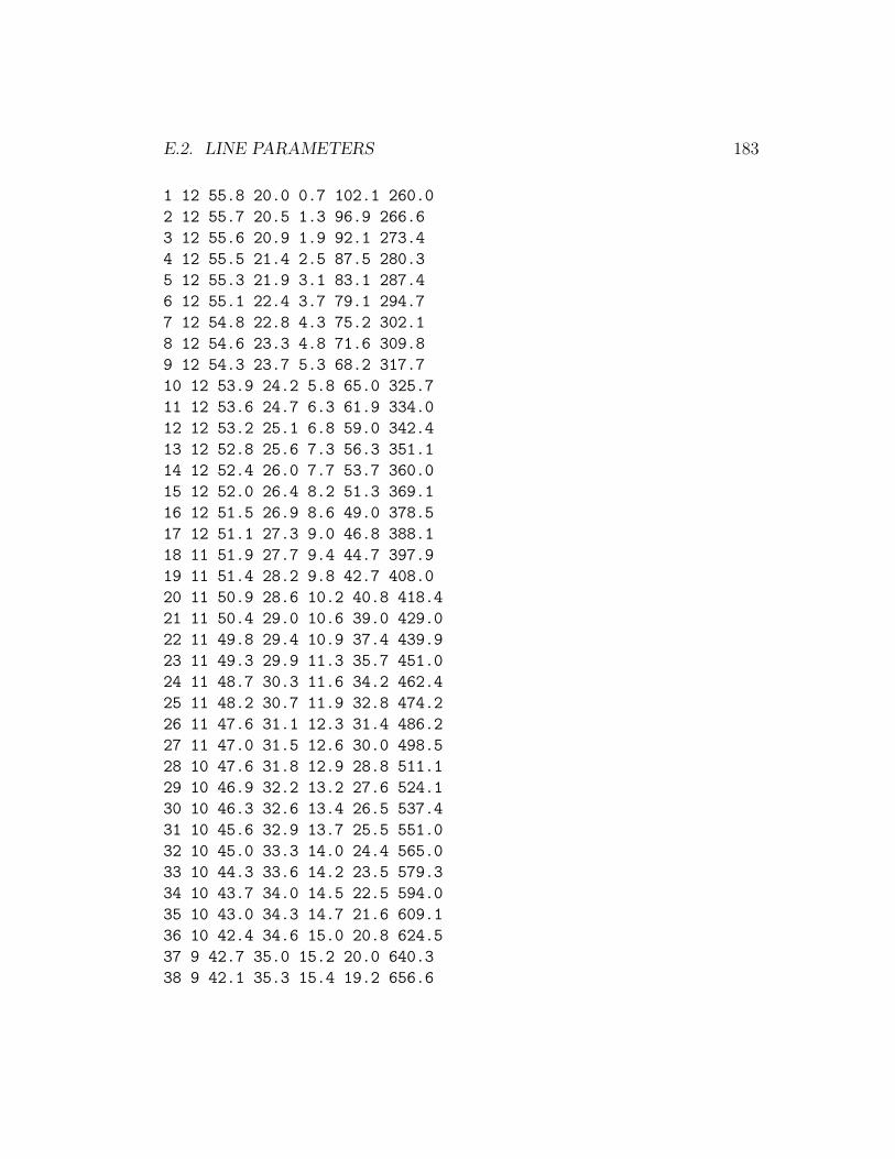
E.2. LINE PARAMETERS 183
1 12 55.8 20.0 0.7 102.1 260.0
2 12 55.7 20.5 1.3 96.9 266.6
3 12 55.6 20.9 1.9 92.1 273.4
4 12 55.5 21.4 2.5 87.5 280.3
5 12 55.3 21.9 3.1 83.1 287.4
6 12 55.1 22.4 3.7 79.1 294.7
7 12 54.8 22.8 4.3 75.2 302.1
8 12 54.6 23.3 4.8 71.6 309.8
9 12 54.3 23.7 5.3 68.2 317.7
10 12 53.9 24.2 5.8 65.0 325.7
11 12 53.6 24.7 6.3 61.9 334.0
12 12 53.2 25.1 6.8 59.0 342.4
13 12 52.8 25.6 7.3 56.3 351.1
14 12 52.4 26.0 7.7 53.7 360.0
15 12 52.0 26.4 8.2 51.3 369.1
16 12 51.5 26.9 8.6 49.0 378.5
17 12 51.1 27.3 9.0 46.8 388.1
18 11 51.9 27.7 9.4 44.7 397.9
19 11 51.4 28.2 9.8 42.7 408.0
20 11 50.9 28.6 10.2 40.8 418.4
21 11 50.4 29.0 10.6 39.0 429.0
22 11 49.8 29.4 10.9 37.4 439.9
23 11 49.3 29.9 11.3 35.7 451.0
24 11 48.7 30.3 11.6 34.2 462.4
25 11 48.2 30.7 11.9 32.8 474.2
26 11 47.6 31.1 12.3 31.4 486.2
27 11 47.0 31.5 12.6 30.0 498.5
28 10 47.6 31.8 12.9 28.8 511.1
29 10 46.9 32.2 13.2 27.6 524.1
30 10 46.3 32.6 13.4 26.5 537.4
31 10 45.6 32.9 13.7 25.5 551.0
32 10 45.0 33.3 14.0 24.4 565.0
33 10 44.3 33.6 14.2 23.5 579.3
34 10 43.7 34.0 14.5 22.5 594.0
35 10 43.0 34.3 14.7 21.6 609.1
36 10 42.4 34.6 15.0 20.8 624.5
37 9 42.7 35.0 15.2 20.0 640.3
38 9 42.1 35.3 15.4 19.2 656.6

184 APPENDIX E. AIR LINE GENERATION PROGRAMS
39 9 41.4 35.6 15.6 18.5 673.2
40 9 40.8 35.9 15.9 17.8 690.3
41 9 40.1 36.2 16.1 17.1 707.8
42 9 39.4 36.6 16.3 16.4 725.7
43 9 38.8 36.9 16.4 15.8 744.1
44 9 38.1 37.2 16.6 15.2 763.0
45 8 38.4 37.4 16.8 14.7 782.3
46 8 37.8 37.8 17.0 14.1 802.2
47 8 37.2 38.2 17.2 13.5 822.5
48 8 36.6 38.5 17.3 13.0 843.4
49 8 36.0 38.9 17.5 12.5 864.7
50 8 35.5 39.2 17.6 12.0 886.7
51 8 34.9 39.5 17.8 11.5 909.1
52 8 34.3 39.8 17.9 11.0 932.2
53 8 33.7 40.2 18.1 10.6 955.8
54 8 33.1 40.5 18.2 10.2 980.1
55 7 33.3 40.8 18.3 9.8 1004.9
56 7 32.8 41.1 18.5 9.4 1030.4
57 7 32.3 41.5 18.6 9.1 1056.5
58 7 31.7 41.8 18.7 8.7 1083.3
59 7 31.2 42.2 18.8 8.3 1110.7
60 7 30.6 42.5 18.9 8.0 1138.9
61 7 30.1 42.8 19.0 7.7 1167.8
62 7 29.6 43.1 19.2 7.4 1197.4
63 7 29.1 43.4 19.3 7.1 1227.7
64 7 28.5 43.7 19.4 6.8 1258.9
65 7 28.0 44.0 19.5 6.6 1290.8
66 7 27.5 44.3 19.5 6.3 1323.5
67 7 27.0 44.6 19.6 6.1 1357.1
68 7 26.5 44.9 19.7 5.9 1391.5
69 7 26.0 45.2 19.8 5.6 1426.7
70 7 25.5 45.5 19.9 5.4 1462.9
71 7 25.0 45.7 20.0 5.2 1500.0
Total attenuation: 3.62
Total diode area: 2175.54
Total line length: 2993.02

E.3. SPICE FILE 185
E.3 SPICE File
! SPICE file for NLTL with 260.00 GHz initial Bragg frequency,
! 1500.00 GHz final Bragg frequency,
! and 20.00 ps total compression.
DIM
LNG UM
CKT
TLINP_T0 201 1 Z=75.00 L=28 K=3.08 A=0.00 F=0.00
S1PA_D1 1 0 [MODEL=VARACTA AREA=102.1] ! fb=260.00
RES_R1 1 301 R=0.3850
TLINP_T1 301 2 Z=75.00 L=56 K=3.08 A=0.00 F=0.00
S1PA_D2 2 0 [MODEL=VARACTA AREA=96.9] ! fb=266.59
RES_R2 2 302 R=0.3844
TLINP_T2 302 3 Z=75.00 L=56 K=3.08 A=0.00 F=0.00
S1PA_D3 3 0 [MODEL=VARACTA AREA=92.1] ! fb=273.35
RES_R3 3 303 R=0.3836
TLINP_T3 303 4 Z=75.00 L=56 K=3.08 A=0.00 F=0.00
S1PA_D4 4 0 [MODEL=VARACTA AREA=87.5] ! fb=280.28
RES_R4 4 304 R=0.3825
TLINP_T4 304 5 Z=75.00 L=55 K=3.08 A=0.00 F=0.00
S1PA_D5 5 0 [MODEL=VARACTA AREA=83.1] ! fb=287.39
RES_R5 5 305 R=0.3813
TLINP_T5 305 6 Z=75.00 L=55 K=3.08 A=0.00 F=0.00
S1PA_D6 6 0 [MODEL=VARACTA AREA=79.1] ! fb=294.67
RES_R6 6 306 R=0.3798
TLINP_T6 306 7 Z=75.00 L=55 K=3.08 A=0.00 F=0.00
S1PA_D7 7 0 [MODEL=VARACTA AREA=75.2] ! fb=302.14
RES_R7 7 307 R=0.3781
TLINP_T7 307 8 Z=75.00 L=55 K=3.08 A=0.00 F=0.00
S1PA_D8 8 0 [MODEL=VARACTA AREA=71.6] ! fb=309.80
RES_R8 8 308 R=0.3763
TLINP_T8 308 9 Z=75.00 L=55 K=3.08 A=0.00 F=0.00
S1PA_D9 9 0 [MODEL=VARACTA AREA=68.2] ! fb=317.66
RES_R9 9 309 R=0.3742
TLINP_T9 309 10 Z=75.00 L=54 K=3.08 A=0.00 F=0.00
S1PA_D10 10 0 [MODEL=VARACTA AREA=65.0] ! fb=325.71
RES_R10 10 310 R=0.3720

186 APPENDIX E. AIR LINE GENERATION PROGRAMS
TLINP_T10 310 11 Z=75.00 L=54 K=3.08 A=0.00 F=0.00
S1PA_D11 11 0 [MODEL=VARACTA AREA=61.9] ! fb=333.97
RES_R11 11 311 R=0.3696
TLINP_T11 311 12 Z=75.00 L=54 K=3.08 A=0.00 F=0.00
S1PA_D12 12 0 [MODEL=VARACTA AREA=59.0] ! fb=342.43
RES_R12 12 312 R=0.3671
TLINP_T12 312 13 Z=75.00 L=53 K=3.08 A=0.00 F=0.00
S1PA_D13 13 0 [MODEL=VARACTA AREA=56.3] ! fb=351.12
RES_R13 13 313 R=0.3644
TLINP_T13 313 14 Z=75.00 L=53 K=3.08 A=0.00 F=0.00
S1PA_D14 14 0 [MODEL=VARACTA AREA=53.7] ! fb=360.02
RES_R14 14 314 R=0.3615
TLINP_T14 314 15 Z=75.00 L=52 K=3.08 A=0.00 F=0.00
S1PA_D15 15 0 [MODEL=VARACTA AREA=51.3] ! fb=369.15
RES_R15 15 315 R=0.3585
TLINP_T15 315 16 Z=75.00 L=52 K=3.08 A=0.00 F=0.00
S1PA_D16 16 0 [MODEL=VARACTA AREA=49.0] ! fb=378.50
RES_R16 16 316 R=0.3554
TLINP_T16 316 17 Z=75.00 L=52 K=3.08 A=0.00 F=0.00
S1PA_D17 17 0 [MODEL=VARACTA AREA=46.8] ! fb=388.10
RES_R17 17 317 R=0.3522
TLINP_T17 317 18 Z=75.00 L=51 K=3.08 A=0.00 F=0.00
S1PA_D18 18 0 [MODEL=VARACTA AREA=44.7] ! fb=397.94
RES_R18 18 318 R=0.3581
TLINP_T18 318 19 Z=75.00 L=52 K=2.92 A=0.00 F=0.00
S1PA_D19 19 0 [MODEL=VARACTA AREA=42.7] ! fb=408.03
RES_R19 19 319 R=0.3547
TLINP_T19 319 20 Z=75.00 L=51 K=2.92 A=0.00 F=0.00
S1PA_D20 20 0 [MODEL=VARACTA AREA=40.8] ! fb=418.37
RES_R20 20 320 R=0.3511
TLINP_T20 320 21 Z=75.00 L=51 K=2.92 A=0.00 F=0.00
S1PA_D21 21 0 [MODEL=VARACTA AREA=39.0] ! fb=428.98
RES_R21 21 321 R=0.3475
TLINP_T21 321 22 Z=75.00 L=50 K=2.92 A=0.00 F=0.00
S1PA_D22 22 0 [MODEL=VARACTA AREA=37.4] ! fb=439.85
RES_R22 22 322 R=0.3438
TLINP_T22 322 23 Z=75.00 L=50 K=2.92 A=0.00 F=0.00
S1PA_D23 23 0 [MODEL=VARACTA AREA=35.7] ! fb=451.01

E.3. SPICE FILE 187
RES_R23 23 323 R=0.3400
TLINP_T23 323 24 Z=75.00 L=49 K=2.92 A=0.00 F=0.00
S1PA_D24 24 0 [MODEL=VARACTA AREA=34.2] ! fb=462.44
RES_R24 24 324 R=0.3361
TLINP_T24 324 25 Z=75.00 L=49 K=2.92 A=0.00 F=0.00
S1PA_D25 25 0 [MODEL=VARACTA AREA=32.8] ! fb=474.16
RES_R25 25 325 R=0.3322
TLINP_T25 325 26 Z=75.00 L=48 K=2.92 A=0.00 F=0.00
S1PA_D26 26 0 [MODEL=VARACTA AREA=31.4] ! fb=486.19
RES_R26 26 326 R=0.3282
TLINP_T26 326 27 Z=75.00 L=48 K=2.92 A=0.00 F=0.00
S1PA_D27 27 0 [MODEL=VARACTB AREA=30.0] ! fb=498.51
RES_R27 27 327 R=0.3241
TLINP_T27 327 28 Z=75.00 L=47 K=2.92 A=0.00 F=0.00
S1PA_D28 28 0 [MODEL=VARACTB AREA=28.8] ! fb=511.15
RES_R28 28 328 R=0.3280
TLINP_T28 328 29 Z=75.00 L=48 K=2.78 A=0.00 F=0.00
S1PA_D29 29 0 [MODEL=VARACTB AREA=27.6] ! fb=524.11
RES_R29 29 329 R=0.3236
TLINP_T29 329 30 Z=75.00 L=47 K=2.78 A=0.00 F=0.00
S1PA_D30 30 0 [MODEL=VARACTB AREA=26.5] ! fb=537.40
RES_R30 30 330 R=0.3192
TLINP_T30 330 31 Z=75.00 L=46 K=2.78 A=0.00 F=0.00
S1PA_D31 31 0 [MODEL=VARACTB AREA=25.5] ! fb=551.02
RES_R31 31 331 R=0.3147
TLINP_T31 331 32 Z=75.00 L=46 K=2.78 A=0.00 F=0.00
S1PA_D32 32 0 [MODEL=VARACTB AREA=24.4] ! fb=564.99
RES_R32 32 332 R=0.3102
TLINP_T32 332 33 Z=75.00 L=45 K=2.78 A=0.00 F=0.00
S1PA_D33 33 0 [MODEL=VARACTB AREA=23.5] ! fb=579.31
RES_R33 33 333 R=0.3057
TLINP_T33 333 34 Z=75.00 L=44 K=2.78 A=0.00 F=0.00
S1PA_D34 34 0 [MODEL=VARACTB AREA=22.5] ! fb=594.00
RES_R34 34 334 R=0.3012
TLINP_T34 334 35 Z=75.00 L=44 K=2.78 A=0.00 F=0.00
S1PA_D35 35 0 [MODEL=VARACTB AREA=21.6] ! fb=609.06
RES_R35 35 335 R=0.2967
TLINP_T35 335 36 Z=75.00 L=43 K=2.78 A=0.00 F=0.00

188 APPENDIX E. AIR LINE GENERATION PROGRAMS
S1PA_D36 36 0 [MODEL=VARACTB AREA=20.8] ! fb=624.50
RES_R36 36 336 R=0.2922
TLINP_T36 336 37 Z=75.00 L=42 K=2.78 A=0.00 F=0.00
S1PA_D37 37 0 [MODEL=VARACTB AREA=20.0] ! fb=640.33
RES_R37 37 337 R=0.2948
TLINP_T37 337 38 Z=75.00 L=43 K=2.64 A=0.00 F=0.00
S1PA_D38 38 0 [MODEL=VARACTB AREA=19.2] ! fb=656.57
RES_R38 38 338 R=0.2902
TLINP_T38 338 39 Z=75.00 L=42 K=2.64 A=0.00 F=0.00
S1PA_D39 39 0 [MODEL=VARACTB AREA=18.5] ! fb=673.21
RES_R39 39 339 R=0.2857
TLINP_T39 339 40 Z=75.00 L=41 K=2.64 A=0.00 F=0.00
S1PA_D40 40 0 [MODEL=VARACTB AREA=17.8] ! fb=690.28
RES_R40 40 340 R=0.2811
TLINP_T40 340 41 Z=75.00 L=41 K=2.64 A=0.00 F=0.00
S1PA_D41 41 0 [MODEL=VARACTB AREA=17.1] ! fb=707.78
RES_R41 41 341 R=0.2765
TLINP_T41 341 42 Z=75.00 L=40 K=2.64 A=0.00 F=0.00
S1PA_D42 42 0 [MODEL=VARACTB AREA=16.4] ! fb=725.72
RES_R42 42 342 R=0.2720
TLINP_T42 342 43 Z=75.00 L=39 K=2.64 A=0.00 F=0.00
S1PA_D43 43 0 [MODEL=VARACTB AREA=15.8] ! fb=744.12
RES_R43 43 343 R=0.2675
TLINP_T43 343 44 Z=75.00 L=39 K=2.64 A=0.00 F=0.00
S1PA_D44 44 0 [MODEL=VARACTB AREA=15.2] ! fb=762.99
RES_R44 44 344 R=0.2630
TLINP_T44 344 45 Z=75.00 L=38 K=2.64 A=0.00 F=0.00
S1PA_D45 45 0 [MODEL=VARACTB AREA=14.7] ! fb=782.33
RES_R45 45 345 R=0.3310
TLINP_T45 345 46 Z=75.00 L=38 K=2.52 A=0.00 F=0.00
S1PA_D46 46 0 [MODEL=VARACTB AREA=14.1] ! fb=802.17
RES_R46 46 346 R=0.3259
TLINP_T46 346 47 Z=75.00 L=38 K=2.52 A=0.00 F=0.00
S1PA_D47 47 0 [MODEL=VARACTB AREA=13.5] ! fb=822.50
RES_R47 47 347 R=0.3208
TLINP_T47 347 48 Z=75.00 L=37 K=2.52 A=0.00 F=0.00
S1PA_D48 48 0 [MODEL=VARACTC AREA=13.0] ! fb=843.36
RES_R48 48 348 R=0.3158

E.3. SPICE FILE 189
TLINP_T48 348 49 Z=75.00 L=37 K=2.52 A=0.00 F=0.00
S1PA_D49 49 0 [MODEL=VARACTC AREA=12.5] ! fb=864.74
RES_R49 49 349 R=0.3107
TLINP_T49 349 50 Z=75.00 L=36 K=2.52 A=0.00 F=0.00
S1PA_D50 50 0 [MODEL=VARACTC AREA=12.0] ! fb=886.66
RES_R50 50 350 R=0.3056
TLINP_T50 350 51 Z=75.00 L=35 K=2.52 A=0.00 F=0.00
S1PA_D51 51 0 [MODEL=VARACTC AREA=11.5] ! fb=909.14
RES_R51 51 351 R=0.3006
TLINP_T51 351 52 Z=75.00 L=35 K=2.52 A=0.00 F=0.00
S1PA_D52 52 0 [MODEL=VARACTC AREA=11.0] ! fb=932.19
RES_R52 52 352 R=0.2956
TLINP_T52 352 53 Z=75.00 L=34 K=2.52 A=0.00 F=0.00
S1PA_D53 53 0 [MODEL=VARACTC AREA=10.6] ! fb=955.82
RES_R53 53 353 R=0.2906
TLINP_T53 353 54 Z=75.00 L=34 K=2.52 A=0.00 F=0.00
S1PA_D54 54 0 [MODEL=VARACTC AREA=10.2] ! fb=980.05
RES_R54 54 354 R=0.2857
TLINP_T54 354 55 Z=75.00 L=33 K=2.52 A=0.00 F=0.00
S1PA_D55 55 0 [MODEL=VARACTC AREA=9.8] ! fb=1004.90
RES_R55 55 355 R=0.3285
TLINP_T55 355 56 Z=75.00 L=33 K=2.40 A=0.00 F=0.00
S1PA_D56 56 0 [MODEL=VARACTC AREA=9.4] ! fb=1030.38
RES_R56 56 356 R=0.3231
TLINP_T56 356 57 Z=75.00 L=33 K=2.40 A=0.00 F=0.00
S1PA_D57 57 0 [MODEL=VARACTC AREA=9.1] ! fb=1056.50
RES_R57 57 357 R=0.3178
TLINP_T57 357 58 Z=75.00 L=32 K=2.40 A=0.00 F=0.00
S1PA_D58 58 0 [MODEL=VARACTC AREA=8.7] ! fb=1083.28
RES_R58 58 358 R=0.3124
TLINP_T58 358 59 Z=75.00 L=32 K=2.40 A=0.00 F=0.00
S1PA_D59 59 0 [MODEL=VARACTC AREA=8.3] ! fb=1110.75
RES_R59 59 359 R=0.3072
TLINP_T59 359 60 Z=75.00 L=31 K=2.40 A=0.00 F=0.00
S1PA_D60 60 0 [MODEL=VARACTC AREA=8.0] ! fb=1138.91
RES_R60 60 360 R=0.3019
TLINP_T60 360 61 Z=75.00 L=31 K=2.40 A=0.00 F=0.00
S1PA_D61 61 0 [MODEL=VARACTC AREA=7.7] ! fb=1167.78

190 APPENDIX E. AIR LINE GENERATION PROGRAMS
RES_R61 61 361 R=0.2967
TLINP_T61 361 62 Z=75.00 L=30 K=2.40 A=0.00 F=0.00
S1PA_D62 62 0 [MODEL=VARACTC AREA=7.4] ! fb=1197.39
RES_R62 62 362 R=0.2915
TLINP_T62 362 63 Z=75.00 L=30 K=2.40 A=0.00 F=0.00
S1PA_D63 63 0 [MODEL=VARACTC AREA=7.1] ! fb=1227.74
RES_R63 63 363 R=0.2863
TLINP_T63 363 64 Z=75.00 L=29 K=2.40 A=0.00 F=0.00
S1PA_D64 64 0 [MODEL=VARACTC AREA=6.8] ! fb=1258.87
RES_R64 64 364 R=0.2812
TLINP_T64 364 65 Z=75.00 L=29 K=2.40 A=0.00 F=0.00
S1PA_D65 65 0 [MODEL=VARACTC AREA=6.6] ! fb=1290.79
RES_R65 65 365 R=0.2761
TLINP_T65 365 66 Z=75.00 L=28 K=2.40 A=0.00 F=0.00
S1PA_D66 66 0 [MODEL=VARACTC AREA=6.3] ! fb=1323.51
RES_R66 66 366 R=0.2711
TLINP_T66 366 67 Z=75.00 L=28 K=2.40 A=0.00 F=0.00
S1PA_D67 67 0 [MODEL=VARACTC AREA=6.1] ! fb=1357.06
RES_R67 67 367 R=0.2661
TLINP_T67 367 68 Z=75.00 L=27 K=2.40 A=0.00 F=0.00
S1PA_D68 68 0 [MODEL=VARACTC AREA=5.9] ! fb=1391.47
RES_R68 68 368 R=0.2612
TLINP_T68 368 69 Z=75.00 L=27 K=2.40 A=0.00 F=0.00
S1PA_D69 69 0 [MODEL=VARACTC AREA=5.6] ! fb=1426.75
RES_R69 69 369 R=0.2563
TLINP_T69 369 70 Z=75.00 L=26 K=2.40 A=0.00 F=0.00
S1PA_D70 70 0 [MODEL=VARACTC AREA=5.4] ! fb=1462.92
RES_R70 70 370 R=0.2515
TLINP_T70 370 71 Z=75.00 L=26 K=2.40 A=0.00 F=0.00
S1PA_D71 71 0 [MODEL=VARACTC AREA=5.2] ! fb=1500.01
RES_R71 71 371 R=0.2467
TLINP_T71 371 72 Z=75.00 L=13 K=2.40 A=0.00 F=0.00
DEF2P 201 72 NLTL
MODEL
VARACTA D RS=105.000000 CJO=1.090000E-15 VJ=0.800000 &
M=0.500000 IS=1.000000E-12 N=1.200000
VARACTB D RS=69.000000 CJO=1.090000E-15 VJ=0.800000 &
M=0.500000 IS=1.000000E-12 N=1.200000

E.4. LAYOUT FILE 191
VARACTC D RS=69.000000 CJO=1.090000E-15 VJ=0.800000 &
M=0.500000 IS=1.000000E-12 N=1.200000
SOURCE
NLTL RES_RIN 201 202 R=50
NLTL IVS_VIN 202 204 TRAN=SIN(0 11.2 30E9 0 0 90)
NLTL RES_RL 72 204 R=50
NLTL IVS_VDC1 204 0 DC=-3.3
CONTROL
NLTL TRAN 10E-12 2E-10
SPICEOUT
NLTL TRAN V(201) V(30) V(60) V(72)
E.4 Layout File
! Academy file for NLTL with 260.00 GHz initial Bragg frequency,
! 1500.00 GHz final Bragg frequency,
! and 25.00 ps total compression.
DIM
LNG UM
CKT
NLTLA_U1 1 2 W=12 GAP=17.0 ADI=102.1 LLI=55.8 ! fb=260.0
NLTLA_U2 2 3 W=12 GAP=17.0 ADI=96.9 LLI=55.7 ! fb=266.6
NLTLA_U3 3 4 W=12 GAP=17.0 ADI=92.1 LLI=55.6 ! fb=273.4
NLTLA_U4 4 5 W=12 GAP=17.0 ADI=87.5 LLI=55.5 ! fb=280.3
NLTLA_U5 5 6 W=12 GAP=17.0 ADI=83.1 LLI=55.3 ! fb=287.4
NLTLA_U6 6 7 W=12 GAP=17.0 ADI=79.1 LLI=55.1 ! fb=294.7
NLTLA_U7 7 8 W=12 GAP=17.0 ADI=75.2 LLI=54.8 ! fb=302.1
NLTLA_U8 8 9 W=12 GAP=17.0 ADI=71.6 LLI=54.6 ! fb=309.8
NLTLA_U9 9 10 W=12 GAP=17.0 ADI=68.2 LLI=54.3 ! fb=317.7
NLTLA_U10 10 11 W=12 GAP=17.0 ADI=65.0 LLI=53.9 ! fb=325.7
NLTLA_U11 11 12 W=12 GAP=17.0 ADI=61.9 LLI=53.6 ! fb=334.0
NLTLA_U12 12 13 W=12 GAP=17.0 ADI=59.0 LLI=53.2 ! fb=342.4
NLTLA_U13 13 14 W=12 GAP=17.0 ADI=56.3 LLI=52.8 ! fb=351.1
NLTLA_U14 14 15 W=12 GAP=17.0 ADI=53.7 LLI=52.4 ! fb=360.0
NLTLA_U15 15 16 W=12 GAP=17.0 ADI=51.3 LLI=52.0 ! fb=369.1
NLTLA_U16 16 17 W=12 GAP=17.0 ADI=49.0 LLI=51.5 ! fb=378.5
NLTLA_U17 17 18 W=12 GAP=17.0 ADI=46.8 LLI=51.1 ! fb=388.1
NLTLA_U18 18 19 W=11 GAP=15.5 ADI=44.7 LLI=51.9 ! fb=397.9
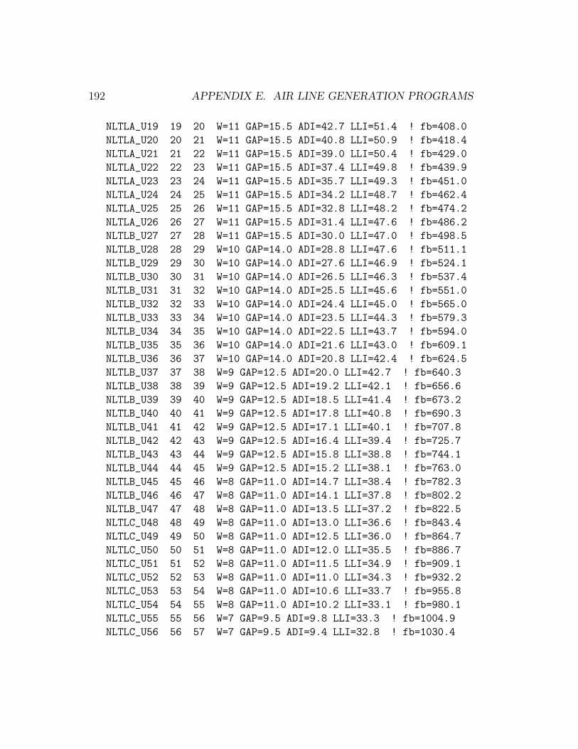
192 APPENDIX E. AIR LINE GENERATION PROGRAMS
NLTLA_U19 19 20 W=11 GAP=15.5 ADI=42.7 LLI=51.4 ! fb=408.0
NLTLA_U20 20 21 W=11 GAP=15.5 ADI=40.8 LLI=50.9 ! fb=418.4
NLTLA_U21 21 22 W=11 GAP=15.5 ADI=39.0 LLI=50.4 ! fb=429.0
NLTLA_U22 22 23 W=11 GAP=15.5 ADI=37.4 LLI=49.8 ! fb=439.9
NLTLA_U23 23 24 W=11 GAP=15.5 ADI=35.7 LLI=49.3 ! fb=451.0
NLTLA_U24 24 25 W=11 GAP=15.5 ADI=34.2 LLI=48.7 ! fb=462.4
NLTLA_U25 25 26 W=11 GAP=15.5 ADI=32.8 LLI=48.2 ! fb=474.2
NLTLA_U26 26 27 W=11 GAP=15.5 ADI=31.4 LLI=47.6 ! fb=486.2
NLTLB_U27 27 28 W=11 GAP=15.5 ADI=30.0 LLI=47.0 ! fb=498.5
NLTLB_U28 28 29 W=10 GAP=14.0 ADI=28.8 LLI=47.6 ! fb=511.1
NLTLB_U29 29 30 W=10 GAP=14.0 ADI=27.6 LLI=46.9 ! fb=524.1
NLTLB_U30 30 31 W=10 GAP=14.0 ADI=26.5 LLI=46.3 ! fb=537.4
NLTLB_U31 31 32 W=10 GAP=14.0 ADI=25.5 LLI=45.6 ! fb=551.0
NLTLB_U32 32 33 W=10 GAP=14.0 ADI=24.4 LLI=45.0 ! fb=565.0
NLTLB_U33 33 34 W=10 GAP=14.0 ADI=23.5 LLI=44.3 ! fb=579.3
NLTLB_U34 34 35 W=10 GAP=14.0 ADI=22.5 LLI=43.7 ! fb=594.0
NLTLB_U35 35 36 W=10 GAP=14.0 ADI=21.6 LLI=43.0 ! fb=609.1
NLTLB_U36 36 37 W=10 GAP=14.0 ADI=20.8 LLI=42.4 ! fb=624.5
NLTLB_U37 37 38 W=9 GAP=12.5 ADI=20.0 LLI=42.7 ! fb=640.3
NLTLB_U38 38 39 W=9 GAP=12.5 ADI=19.2 LLI=42.1 ! fb=656.6
NLTLB_U39 39 40 W=9 GAP=12.5 ADI=18.5 LLI=41.4 ! fb=673.2
NLTLB_U40 40 41 W=9 GAP=12.5 ADI=17.8 LLI=40.8 ! fb=690.3
NLTLB_U41 41 42 W=9 GAP=12.5 ADI=17.1 LLI=40.1 ! fb=707.8
NLTLB_U42 42 43 W=9 GAP=12.5 ADI=16.4 LLI=39.4 ! fb=725.7
NLTLB_U43 43 44 W=9 GAP=12.5 ADI=15.8 LLI=38.8 ! fb=744.1
NLTLB_U44 44 45 W=9 GAP=12.5 ADI=15.2 LLI=38.1 ! fb=763.0
NLTLB_U45 45 46 W=8 GAP=11.0 ADI=14.7 LLI=38.4 ! fb=782.3
NLTLB_U46 46 47 W=8 GAP=11.0 ADI=14.1 LLI=37.8 ! fb=802.2
NLTLB_U47 47 48 W=8 GAP=11.0 ADI=13.5 LLI=37.2 ! fb=822.5
NLTLC_U48 48 49 W=8 GAP=11.0 ADI=13.0 LLI=36.6 ! fb=843.4
NLTLC_U49 49 50 W=8 GAP=11.0 ADI=12.5 LLI=36.0 ! fb=864.7
NLTLC_U50 50 51 W=8 GAP=11.0 ADI=12.0 LLI=35.5 ! fb=886.7
NLTLC_U51 51 52 W=8 GAP=11.0 ADI=11.5 LLI=34.9 ! fb=909.1
NLTLC_U52 52 53 W=8 GAP=11.0 ADI=11.0 LLI=34.3 ! fb=932.2
NLTLC_U53 53 54 W=8 GAP=11.0 ADI=10.6 LLI=33.7 ! fb=955.8
NLTLC_U54 54 55 W=8 GAP=11.0 ADI=10.2 LLI=33.1 ! fb=980.1
NLTLC_U55 55 56 W=7 GAP=9.5 ADI=9.8 LLI=33.3 ! fb=1004.9
NLTLC_U56 56 57 W=7 GAP=9.5 ADI=9.4 LLI=32.8 ! fb=1030.4

E.5. ACADEMY MACROS 193
NLTLC_U57 57 58 W=7 GAP=9.5 ADI=9.1 LLI=32.3 ! fb=1056.5
NLTLC_U58 58 59 W=7 GAP=9.5 ADI=8.7 LLI=31.7 ! fb=1083.3
NLTLC_U59 59 60 W=7 GAP=9.5 ADI=8.3 LLI=31.2 ! fb=1110.7
NLTLC_U60 60 61 W=7 GAP=9.5 ADI=8.0 LLI=30.6 ! fb=1138.9
NLTLC_U61 61 62 W=7 GAP=9.5 ADI=7.7 LLI=30.1 ! fb=1167.8
NLTLC_U62 62 63 W=7 GAP=9.5 ADI=7.4 LLI=29.6 ! fb=1197.4
NLTLC_U63 63 64 W=7 GAP=9.5 ADI=7.1 LLI=29.1 ! fb=1227.7
NLTLC_U64 64 65 W=7 GAP=9.5 ADI=6.8 LLI=28.5 ! fb=1258.9
NLTLC_U65 65 66 W=7 GAP=9.5 ADI=6.6 LLI=28.0 ! fb=1290.8
NLTLC_U66 66 67 W=7 GAP=9.5 ADI=6.3 LLI=27.5 ! fb=1323.5
NLTLC_U67 67 68 W=7 GAP=9.5 ADI=6.1 LLI=27.0 ! fb=1357.1
NLTLC_U68 68 69 W=7 GAP=9.5 ADI=5.9 LLI=26.5 ! fb=1391.5
NLTLC_U69 69 70 W=7 GAP=9.5 ADI=5.6 LLI=26.0 ! fb=1426.7
NLTLC_U70 70 71 W=7 GAP=9.5 ADI=5.4 LLI=25.5 ! fb=1462.9
NLTLC_U71 71 72 W=7 GAP=9.5 ADI=5.2 LLI=25.0 ! fb=1500.0
DEF2P 1 72 NLTL71
E.5 Academy Macros
! Macro Programs for Air Bridged Lines
! Scott Allen 10/93
!
! Definitions for the different point types
!
iboc = 3 ! point type for begin open contour
ibccf= 4 ! point type for begin closed contour, filled
ibcce= 5 ! point type for begin closed contour, empty
ibcir= 6 ! point type for begin circle (give center)
ibhol= 7 ! point type for begin hole (give center x,y)
icon = 8 ! point type for connecting point
iarc = 9 ! point type for begin arc (give radius, sweep angle in degrees)
icen = 10 ! point type for end arc (give center x,y)
ieoc = 11 ! point type for end open contour
iecc = 12 ! point type for end closed contour
iecir= 13 ! point type for end circle (give radius, 2nd value ignored)
iiso = 14 ! point type for isolated point
!
! Definitions of the different layers

194 APPENDIX E. AIR LINE GENERATION PROGRAMS
!
schint = 0 ! schottky contacts and interconnect
ohmic = 1 ! ohmic metal
isolation = 2 ! ion implant isolation
nitride = 3 ! silicon nitride mask
post = 4 ! air bridge post & capacitor contact
ab = 5 ! air bridge
hr = 6 ! high-res mask, 1 um features
!
!------------------------------------------------------------------------------------
!
! Line Layout Program for MACRO "NLTLA"
! Air bridged center conductor, ground plane diodes, 2um Schottky fingers
! Line tapers down to 8um at the diode
! Written by Scott Allen 10/93
!
defelem "NLTLA",2,"w","gap","adi","lli"
real w,gap,adi,lli,ldi,ctr,dx,dy,g
lli=int(0.5+lli)
w=int(0.5+w)
lam=int(0.5+lam)
ldi=0.5*int(0.5+adi/2)+.5 !add 0.5um to account for ion straggle
! Find center of the line section:
ctr=0.5*lli
g=2*(w+2*gap)
!
! Air Bridged Center Conductor
level ab
dy=(w-8)/2
dx=(lli-22)/2-dy ! 18 is total width of where ohmics are
point ibccf,0,w/-2
node n1,0,0
point icon,0,w/2
point icon,dx,w/2
point icon,dx+dy,w/2-dy
point icon,lli-dx-dy,w/2-dy
point icon,lli-dx,w/2
point icon,lli,w/2

E.5. ACADEMY MACROS 195
node n2,lli,0
point icon,lli,w/-2
point icon,lli-dx,w/-2
point icon,lli-dx-dy,w/-2+dy
point icon,dx+dy,w/-2+dy
point iecc,dx,w/-2
!
! Post to Schottky Diode
level post
dx=2.5
dy=2.5
point ibccf,ctr-dx,dy
point icon,ctr+dx,dy
point icon,ctr+dx,-dy
point iecc,ctr-dx,-dy
!
! Schottky Diodes and Ground Plane
level schint
dx=1 ! center of Schottky stripe
dy=12 ! 4 from center line + 2 for spacing + 2 for ohmics
! diode stripe
point ibccf,ctr-dx,dy+ldi
point icon,ctr+dx,dy+ldi
point icon,ctr+dx,-dy-ldi
point iecc,ctr-dx,-dy-ldi
! upper ground plane
dx=5 ! center of Schottky to ohmic
point ibccf,0,gap
point icon,0,(gap+g)
point icon,lli,(gap+g)
point icon,lli,(gap)
point icon,ctr+dx+4,(gap)
point icon,ctr+dx+4,(dy+ldi+8)
point icon,ctr-dx-4,(dy+ldi+8)
point iecc,ctr-dx-4,(gap)
!lower ground plane
point ibccf,0,-gap
point icon,0,-(gap+g)

196 APPENDIX E. AIR LINE GENERATION PROGRAMS
point icon,lli,-(gap+g)
point icon,lli,-(gap)
point icon,ctr+dx+4,-(gap)
point icon,ctr+dx+4,-(dy+ldi+8)
point icon,ctr-dx-4,-(dy+ldi+8)
point iecc,ctr-dx-4,-(gap)
!
! Ohmics
level ohmic
dx=5 ! center of Schottky stripe to ohmic
dy=8 ! edge of ohmic: 4 + 2um space
! upper ohmic
point ibccf,ctr-dx,(dy)
point icon,ctr-dx-8,(dy)
point icon,ctr-dx-8,(dy+ldi+18)
point icon,ctr+dx+8,(dy+ldi+18)
point icon,ctr+dx+8,(dy)
point icon,ctr+dx,(dy)
point icon,ctr+dx,(dy+ldi+8)
point iecc,ctr-dx,(dy+ldi+8)
!lower ohmic
point ibccf,ctr-dx,-(dy)
point icon,ctr-dx-8,-(dy)
point icon,ctr-dx-8,-(dy+ldi+18)
point icon,ctr+dx+8,-(dy+ldi+18)
point icon,ctr+dx+8,-(dy)
point icon,ctr+dx,-(dy)
point icon,ctr+dx,-(dy+ldi+8)
point iecc,ctr-dx,-(dy+ldi+8)
! ground straps
point ibccf,ctr+dx+8,dy
point icon,ctr+dx+6,dy
point icon,ctr+dx+6,-dy
point iecc,ctr+dx+8,-dy
!
level isolation
dy=12 ! 4 + 2 spacing + 2 ohmics
point ibccf,ctr-17,dy

E.5. ACADEMY MACROS 197
point icon,ctr-17,(dy+ldi+12)
point icon,ctr+17,(dy+ldi+12)
point iecc,ctr+17,dy
!
point ibccf,ctr-17,-dy
point icon,ctr-17,-(dy+ldi+12)
point icon,ctr+17,-(dy+ldi+12)
point iecc,ctr+17,-dy
!
end define
!
!----------------------------------------------------------------------------
!
! Line Layout Program for MACRO "NLTLB"
! Air bridged center conductor, ground plane diodes, 1um Schottky fingers
! Line tapers down to 8um at the diode
! Written by Scott Allen 10/93
!
defelem "NLTLB",2,"w","gap","adi","lli"
real w,gap,adi,lli,ldi,ctr,dx,dy,g
lli=int(0.5+lli)
w=int(0.5+w)
lam=int(0.5+lam)
ldi=0.5*int(0.5+adi)+.5 ! add 0.5um to account for ion straggle
! Find center of the line section:
ctr=0.5*lli
g=2*(w+2*gap)
!
! Air Bridged Center Conductor
level ab
dy=(w-8)/2
dx=(lli-21)/2-dy ! 17um is total width of where ohmics are
point ibccf,0,w/-2
node n1,0,0
point icon,0,w/2
point icon,dx,w/2
point icon,dx+dy,w/2-dy
point icon,lli-dx-dy,w/2-dy

198 APPENDIX E. AIR LINE GENERATION PROGRAMS
point icon,lli-dx,w/2
point icon,lli,w/2
node n2,lli,0
point icon,lli,w/-2
point icon,lli-dx,w/-2
point icon,lli-dx-dy,w/-2+dy
point icon,dx+dy,w/-2+dy
point iecc,dx,w/-2
!
! Post to Schottky Diode
level post
dx=2.5
dy=2.5
point ibccf,ctr-dx,dy
point icon,ctr+dx,dy
point icon,ctr+dx,-dy
point iecc,ctr-dx,-dy
!
! Schottky Diodes and Ground Plane
level schint
dx=0.5 ! center of Schottky stripe
dy=12 ! 8/2 from center line + 2 for spacing + 2 for ohmics
! diode stripe
point ibccf,ctr-dx,dy+ldi
point icon,ctr+dx,dy+ldi
point icon,ctr+dx,-dy-ldi
point iecc,ctr-dx,-dy-ldi
! 1 x 3 cross post
point ibccf,ctr-1.5,0.5
point icon,ctr+1.5,0.5
point icon,ctr+1.5,-0.5
point iecc,ctr-1.5,-0.5
! upper ground plane
dx=4.5 ! spacing from center of Schottky to ohmic
point ibccf,0,gap
point icon,0,(gap+g)
point icon,lli,(gap+g)
point icon,lli,(gap)

E.5. ACADEMY MACROS 199
point icon,ctr+dx+4,(gap)
point icon,ctr+dx+4,(dy+ldi+8)
point icon,ctr-dx-4,(dy+ldi+8)
point iecc,ctr-dx-4,(gap)
!lower ground plane
point ibccf,0,-gap
point icon,0,-(gap+g)
point icon,lli,-(gap+g)
point icon,lli,-(gap)
point icon,ctr+dx+4,-(gap)
point icon,ctr+dx+4,-(dy+ldi+8)
point icon,ctr-dx-4,-(dy+ldi+8)
point iecc,ctr-dx-4,-(gap)
!
! Ohmics
level ohmic
dx=4.5 ! center of Schottky stripe to ohmic
dy=8 ! edge of ohmic: 8/2 + 2um space
! upper ohmic
point ibccf,ctr-dx,(dy)
point icon,ctr-dx-8,(dy)
point icon,ctr-dx-8,(dy+ldi+18)
point icon,ctr+dx+8,(dy+ldi+18)
point icon,ctr+dx+8,(dy)
point icon,ctr+dx,(dy)
point icon,ctr+dx,(dy+ldi+8)
point iecc,ctr-dx,(dy+ldi+8)
!lower ohmic
point ibccf,ctr-dx,-(dy)
point icon,ctr-dx-8,-(dy)
point icon,ctr-dx-8,-(dy+ldi+18)
point icon,ctr+dx+8,-(dy+ldi+18)
point icon,ctr+dx+8,-(dy)
point icon,ctr+dx,-(dy)
point icon,ctr+dx,-(dy+ldi+8)
point iecc,ctr-dx,-(dy+ldi+8)
! ground straps
point ibccf,ctr+dx+8,dy

200 APPENDIX E. AIR LINE GENERATION PROGRAMS
point icon,ctr+dx+6,dy
point icon,ctr+dx+6,-dy
point iecc,ctr+dx+8,-dy
!
level isolation
dy=12 ! 8/2 + 2 spacing + 2 ohmics
point ibccf,ctr-17,dy
point icon,ctr-17,(dy+ldi+12)
point icon,ctr+17,(dy+ldi+12)
point iecc,ctr+17,dy
!
point ibccf,ctr-17,-dy
point icon,ctr-17,-(dy+ldi+12)
point icon,ctr+17,-(dy+ldi+12)
point iecc,ctr+17,-dy
!
end define
!
!----------------------------------------------------------------------------
!
! Line Layout Program for MACRO "NLTLC"
! Air bridged center conductor, center diodes, 1um Schottky fingers
! Written by Scott Allen 10/93
!
defelem "NLTLC",2,"w","gap","adi","lli"
real w,gap,adi,lli,ldi,ctr,dx,dy,g
lli=int(0.5+lli)
w=int(0.5+w)
lam=int(0.5+lam)
ldi=0.5*int(0.5+adi)
! Find center of the line section:
ctr=0.5*lli
g=2*(w+2*gap)
!
! Air Bridged Center Conductor
level ab
dy=(w-9)/2
dx=ctr-ldi-2-dy

E.5. ACADEMY MACROS 201
point ibccf,0,w/-2
node n1,0,0
point icon,0,w/2
point icon,lli,w/2
node n2,lli,0
point iecc,lli,w/-2
!
! Post to Schottky Diode
level post
dx=3.5
dy=2.5
point ibccf,ctr-dx,dy
point icon,ctr+dx,dy
point icon,ctr+dx,-dy
point iecc,ctr-dx,-dy
!
! Schottky Diodes and Ground Plane
level schint
dy=.5
! diode stripe
point ibccf,ctr-ldi,dy
point icon,ctr+ldi,dy
point icon,ctr+ldi,-dy
point iecc,ctr-ldi,-dy
! upper ground plane
dx=3 ! center of Schottky to ohmic
point ibccf,0,gap
point icon,0,(gap+g)
point icon,lli,(gap+g)
point iecc,lli,(gap)
!lower ground plane
point ibccf,0,-gap
point icon,0,-(gap+g)
point icon,lli,-(gap+g)
point iecc,lli,-(gap)
! Extra metal on ohmic pads
dy=4.5
point ibccf,ctr-ldi,dy

202 APPENDIX E. AIR LINE GENERATION PROGRAMS
point icon,ctr-ldi,gap
point icon,ctr+ldi,gap
point iecc,ctr+ldi,dy
!
point ibccf,ctr-ldi,-dy
point icon,ctr-ldi,-gap
point icon,ctr+ldi,-gap
point iecc,ctr+ldi,-dy
!
! Ohmics
level ohmic
dx=2
dy=2.5
! upper ohmic
point ibccf,ctr-ldi-dx,(dy)
point icon,ctr-ldi-dx,(gap+6)
point icon,ctr+ldi+dx,(gap+6)
point iecc,ctr+ldi+dx,(dy)
!lower ohmic
point ibccf,ctr-ldi-dx,-(dy)
point icon,ctr-ldi-dx,-(gap+6)
point icon,ctr+ldi+dx,-(gap+6)
point iecc,ctr+ldi+dx,-(dy)
!
level isolation
dx=4
point ibccf,ctr-ldi-dx,gap+4
point icon,ctr+ldi+dx,gap+4
point icon,ctr+ldi+dx,-gap-4
point iecc,ctr-ldi-dx,-gap-4
!
end define
!----------------------------------------------------------------------------
! Line layout for center conductor didoes in normal Schottky metal
! Written by Mike Case 7/92
!
defelem "NLTLD",2,"z","w","adi","lli","lam","lams","lamo"
real z,x,y,w,adi,lli,b,g,ldi,lam,ctr,lams,lamo

E.5. ACADEMY MACROS 203
lli=0.5*int(0.5+2*lli)
w=int(0.5+w)
lam=int(0.5+lam)
lams=int(0.5+lams)
lamo=int(0.5+lamo)
ldi=int(0.5+adi/lams)
ctr=0.5*int(0.5+lli)
! Check it out
if w < lams then
w=lams
end if
! Find gap
x=sqr(1-((0.5*exp(z/11.33893419)-1)/(0.5*exp(z/11.33893419)+1))^4)
! X=w/(w+2b)
y=(1-x)/(2*x)
b=0.5*int(0.5+2*y*w)
! Find ground width
g=2*int(0.5+w/x)
level schint
! Center
if w = lams then
point ibccf,0,w/-2
node n1,0,0
point icon,0,w/2
point icon,lli,w/2
node n2,lli,0
point iecc,lli,w/-2
else
point ibccf,0,w/-2
node n1,0,0
point icon,0,w/2
point icon,ctr-ldi/2-2*lam,w/2
point icon,ctr-ldi/2-2*lam,lams/2
point icon,ctr+ldi/2+2*lam,lams/2
point icon,ctr+ldi/2+2*lam,w/2
point icon,lli,w/2
node n2,lli,0
point icon,lli,w/-2

204 APPENDIX E. AIR LINE GENERATION PROGRAMS
point icon,ctr+ldi/2+2*lam,w/-2
point icon,ctr+ldi/2+2*lam,lams/-2
point icon,ctr-ldi/2-2*lam,lams/-2
point iecc,ctr-ldi/2-2*lam,w/-2
end if
! Upper ground
point ibccf,0,w/2+b
point icon,0,w/2+b+g
point icon,lli,w/2+b+g
point icon,lli,w/2+b
point icon,ctr+ldi/2,w/2+b
point icon,ctr+ldi/2,lams/2+lamo+lam
point icon,ctr-ldi/2,lams/2+lamo+lam
point iecc,ctr-ldi/2,w/2+b
! Lower ground
point ibccf,0,-1*(w/2+b)
point icon,0,-1*(w/2+b+g)
point icon,lli,-1*(w/2+b+g)
point icon,lli,-1*(w/2+b)
point icon,ctr+ldi/2,-1*(w/2+b)
point icon,ctr+ldi/2,-1*(lams/2+lamo+lam)
point icon,ctr-ldi/2,-1*(lams/2+lamo+lam)
point iecc,ctr-ldi/2,-1*(w/2+b)
! Now ohmics
level ohmic
! Upper
point ibccf,ctr-ldi/2-lam,lams/2+lamo
point icon,ctr-ldi/2-lam,w/2+b+lam
point icon,ctr+ldi/2+lam,w/2+b+lam
point iecc,ctr+ldi/2+lam,lams/2+lamo
! Lower
point ibccf,ctr-ldi/2-lam,-1*(lams/2+lamo)
point icon,ctr-ldi/2-lam,-1*(w/2+b+lam)
point icon,ctr+ldi/2+lam,-1*(w/2+b+lam)
point iecc,ctr+ldi/2+lam,-1*(lams/2+lamo)
! finally, the ion implant
level isolation
if ldi < 8 then

E.5. ACADEMY MACROS 205
point ibccf,ctr-4,-1*(w/2+b+8*lam)
point icon,ctr-4,-1*(w/2+b+2*lam)
point icon,ctr-ldi/2,-1*(w/2+b+2*lam)
point icon,ctr-ldi/2,w/2+b+2*lam
point icon,ctr-4,w/2+b+2*lam
point icon,ctr-4,w/2+b+8*lam
point icon,ctr+4,w/2+b+8*lam
point icon,ctr+4,w/2+b+2*lam
point icon,ctr+ldi/2,w/2+b+2*lam
point icon,ctr+ldi/2,-1*(w/2+b+2*lam)
point icon,ctr+4,-1*(w/2+b+2*lam)
point iecc,ctr+4,-1*(w/2+b+8*lam)
else
point ibccf,ctr-ldi/2,-1*(w/2+b+2*lam)
point icon,ctr-ldi/2,w/2+b+2*lam
point icon,ctr+ldi/2,w/2+b+2*lam
point iecc,ctr+ldi/2,-1*(w/2+b+2*lam)
end if
end define

206 APPENDIX E. AIR LINE GENERATION PROGRAMS

Bibliography
[1] U.K. Mishra, A.S. Brown, and S.E. Rosenbaum, “DC and RF performanceof 0.1 µm gate length AlInAs-GaInAs pseudomorphic HEMT’s,” 1988 Inter-national Electron Devices Technical Digest, pp. 1407-1410, San Francisco,CA, December, 1988.
[2] M.J.W. Rodwell, M. Kamegawa, R.Y. Yu, M.G. Case, E. Carman, and K.S.Giboney, “GaAs nonlinear transmission lines for picosecond generation andmillimeter-wave sampling,” Microwave Theory and Techniques, vol. MTT-39, no. 7, pp. 1194-1204, July, 1991.
[3] R.Y. Yu, M.G. Case, M. Kamegawa, M. Sundaram, M.J.W. Rodwell, andA.W. Gossard, “275 GHz 3-mask integrated GaAs sampling circuit,” Elec-tronics Letters, vol. 26, no. 13, pp. 949-950, 21 June, 1990.
[4] M.J.W. Rodwell, D.M. Bloom, and B.A. Auld, “Generation of 7.8 ps elec-trical transients on a monolithic nonlinear transmission line,” ElectronicsLetters, vol. 24, no. 2, p. 100, 21 January, 1988.
[5] C.J. Madden, R.A. Marsland, M.J.W. Rodwell, D.M. Bloom, and Y.C.Pao, “Hyperabrupt-doped GaAs nonlinear transmission line for picosecondshock-wave generation,” Applied Physics Letters, vol. 54, no. 11, pp. 1019-1021, March 13, 1989.
[6] HP5412T 50 GHz Digitizing Oscilloscope, Hewlett-Packard Co., SantaClara, CA.
[7] M.G. Case, R.Y. Yu, M. Kamegawa, M. Sundaram, M.J.W. Rodwell, andA.C. Gossard, “Accurate 225 GHz sampling circuit implemented in a 3-mask process,” I.E.E.E. Device Research Conference, Santa Barbara, CA,June, 1990.
207

208 BIBLIOGRAPHY
[8] Y. Konishi, M. Kamegawa, M. Case, R. Yu, M.J.W. Rodwell, and D.B. Rut-ledge, “Picosecond spectroscopy using monolithic GaAs circuits,” AppliedPhysics Letters, vol. 61, no. 23, December 7, 1992.
[9] R.Y. Yu, M. Reddy, J. Pusl, S. Allen, M. Case, and M.J.W. Rodwell, “Fulltwo-port on-wafer vector network analysis to 120 GHz using active probes,”1993 IEE International Microwave Symposium Digest, pp. 1339-1342, At-lanta, GA, June, 1993.
[10] R. Landauer, “Shock waves in nonlinear transmission lines and their effecton parametric amplification,” IBM Journal of Research and Development,vol. 4, no. 4, pp. 391-401, October, 1960.
[11] R. Landauer, “Shock wave structure in nonlinear dielectrics,” Ferroelectrics,vol. 10, pp. 237-240, 1976.
[12] M. Case, E. Carman, R. Yu, M.J.W. Rodwell, and M. Kamegawa, “Picosec-ond duration, large-amplitude impulse generation using electrical solitoneffects,” Applied Physics Letters, vol. 60, no. 24, pp. 3019-3021, June 15,1992.
[13] R.K. Hoffman, Handbook of Microwave Integrated Circuits, Artech House,1987.
[14] P.A.D. Wood, W.C.B. Peatman, D.W. Porterfield, and T.W. Crowe, “GaAsSchottky diodes for THz mixing applications,” Proceedings of the FourthInternational Symposium on Space Terahertz Technology, pp. 377-391, LosAngeles, CA, March, 1993.
[15] T.W. Crowe, R.J. Mattauch, H.P. Roser, W.L. Bishop, W.C.B. Peatman,and X. Liu, “GaAs Schottky diodes for THz mixing applications,” IEEEProceedings, vol. 80, no. 11, pp. 1827-1841, November, 1992.
[16] K. S. Champlin and G. Eisenstein, “Cutoff frequency of submillimeterSchottky-barrier diodes,” Microwave Theory and Techniques, vol. MTT-26,no. 1, pp. 31-34, January, 1978.
[17] L.E. Dickens, “Spreading resistance as a function of frequency” MicrowaveTheory and Techniques, vol. MTT-15, no. 2, pp. 101-109, February, 1967.

BIBLIOGRAPHY 209
[18] K. S. Champlin, D.B. Armstrong and P.D. Gunderson, “Charge carrierinertia in semiconductors,” Proceedings of I.R.E., vol. 52, no. 6, pp. 677-685, June, 1964.
[19] B. Gelmont, M. Shur, and R.J. Mattauch, “Capacitance-voltage character-istics of microwave Schottky diodes,” Microwave Theory and Techniques,vol. MTT-39, no. 5, pp. 857-862, May, 1991.
[20] R.E. Williams, Gallium Arsenide Processing Techniques, Artech House,Dedham, MA, 1984.
[21] D.C. D’Avanzo, “Proton isolation for GaAs integrated circuits,” I.E.E.E.Transactions on Electron Devices, vol. ED-29, pp. 1051-1059, July, 1982.
[22] J.F. Gibbons, W.S. Johnson, and S.W. Mylorie, Projected Range Statistics:Semiconductors and Related Materials, Dowden, Hutchinson, and Ross,Stroudsburg, PA, 1975.
[23] J.W. Coburn, “Plasma etching and reactive ion etching,” American VacuumSociety Monograph Series, 1982.
[24] G.A. Vawter, L.A. Coldren, J.L. Merz, and E.L. Hu, “Nonselective etchingof GaAs/AlGaAs double heterostructure laser facets by Cl2 reactive ionetching in a load-locked system,” Applied Physics Letters, vol. 51, no. 10,pp. 719-721, September 7, 1987.
[25] J.M. Golio, M.G. Miller, G.N. Maracas, and D.A. Johnson, “Frequency-dependent electrical characteristics of GaAs MESFET’s,” Microwave The-ory and Techniques, vol. MTT-37, no. 5, pp. 1217-1227, May, 1990.
[26] S.M. Sze, Physics of Semiconductor Devices, John Wiley and Sons, NewYork, 1981.
[27] S. Lautzenhiser, A. Davidson, and K. Jones, “Improve accuracy of on- wafertests via LRM calibration,” Microwaves and RF, January, 1990.
[28] R.A. York, unpublished analysis.
[29] J.C. Yi, S.H. Kim, and S.S. Choi, “Finite-element method for the impedanceanalysis of traveling-wave modulators,” Journal of Lightwave Technology,vol. 8, no. 6, pp. 817-822, June, 1990.

210 BIBLIOGRAPHY
[30] M.S. Shakouri, A. Black, B.A. Auld, and D.M. Bloom, “500 GHz MMICsampling wafer probe,” Electronic Letters, vol. 29, no. 6, pp. 557-558, 18March, 1993.
[31] R. Nagarajan, T. Fukushima, J. E. Bowers, R. S. Geels, and L. A. Coldren,“High speed InGaAs/GaAs strained multiple quantum well lasers with lowdamping,” Applied Physics Letters, vol. 58, no. 21, pp. 2326-2328, May1991.
[32] M. Hafizi, W.E. Stanchina, R.A. Metzger, J.F. Jensen, and F. Williams,“Reliability of AlInAs/GaInAs HBT’s,” Transactions on Electron Devices,vol. 40, no. 12, pp. 2178-2185, December, 1993.
[33] Shipley Company, Inc., Newton, MA.
[34] M.S. Shakouri, A. Black, D.M. Bloom, J. Perdomo, H. Kondoh, and H.Vifian, “Picosecond MODFET IC pulse sharpener,” Monolithic CircuitsSymposium Digest, pp. 79-81, Atlanta, GA, June, 1993.
[35] E.L. Kollberg, T.J. Tolmunen, M.A. Frerking, and J.R. East, “Current satu-ration in submillimeter wave varactors,” Microwave Theory and Techniques,vol. MTT-40, no. 5, pp. 831-838, May, 1992.
[36] T.W. Crowe, W.C.B. Peatman, R. Zimmermann, and R. Zimmermann,“Consideration of velocity saturation in the design of varactor diodes,” Mi-crowave and Guided Wave Letters, vol. 3, no. 6, pp. 161-163, June, 1993.
[37] E.R. Brown, T.C.L.G. Sollner, C.D. Parker, W.D. Goodhue, and C.L. Chen,“Oscillations up to 420 GHz in GaAs/AlAs resonant tunneling diodes,”Applied Physics Letters, vol. 55, no. 23, pp. 1777-1779, October 23, 1989.
[38] E.R. Brown, J.R. Soderstrom, C.D. Parker, L.J. Mahoney, K.M. Molvar,and T.C. McGill, “Oscillations up to 712 GHz in InAs/AlSb resonant-tunneling diodes,” Applied Physics Letters, vol. 58, no. 20, pp.2291-2293,May 20, 1991.
[39] R.C. Tiberio, J.M. Limber, G.J. Galvin, and E.D. Wolf, “Electron-beamlithography and resist processing for the fabrication of T-gate struc-tures,” Electron- Beam, X-Ray, and Ion-Beam Technology: submicrometerLithographies VIII, SPIE vol. 1089, pp. 124-131, 1989.

BIBLIOGRAPHY 211
[40] A.C. Seabaugh, A.H. Taddiken, E.A. Beam III, J.N. Randall, Y.C. Kao, andB. Newell, “Co-integrated resonant tunneling and heterojunction bipolartransistor full adder,” 1993 International Electron Devices Meeting Techni-cal Digest, pp. 407-410, Washington, DC, December, 1993.
[41] H. Kroemer, Quantum Mechanics, Prentice Hall, New Jersey, 1994.
[42] E.R. Brown, C.D. Parker, and T.C.L.G. Sollner, “Quantum well lifetime andits effect on the frequency response of resonant tunneling diodes,” AppliedPhysics Letters, vol. 54, pp. 934-936, 1989.
[43] E.R. Brown, “Resonant tunneling in high-speed double barrier diodes,” HotElectrons in Semiconductor Heterostructures, J. Shah, ed., Academic Press,Boston, 1991.
[44] E.R. Brown, C.D. Parker, A.R. Calawa, M.J. Manfra, T.C.L.G. Sollner, C.L.Chen, S.W. Pang, and K.M. Kolvar, “High-speed resonant-tunneling diodesmade from the InGaAs/AlAs material system,” High-Speed Electronics andDevice Scaling, SPIE vol. 1288, pp. 122-135, 1990.
[45] A. Ketterson, M. Tong, J.W. Seo, K. Nummila, Y.K. Cheng, J. Morikuni, S.Kang, and I. Adesida, “Submicron modulation-doped field-effect transistor-metal/semiconductor-metal-based optoelectronic integrated circuit receiverfabricated by direct-write electron-beam lithography,” Journal of VacuumScience Technology B, vol. 10, no. 6, pp. 2936-2940, Nov/Dec, 1992.
[46] D.H. Chow, J.N. Schulman, E. Ozbay, and D.M. Bloom, “Investigations ofInGaAs/AlAs resonant tunneling diodes for high speed switching,” AppliedPhysics Letters, vol. 61, no. 14, pp. 1685-1687, October 5, 1992.