se12864wrf-039-h-q spec v001 · colorimeter=bm-7 fast 500 ㎜ data modul ag - 6. note 1. optical...
TRANSCRIPT

Specification
BTHQ 128064AVO-FETF-06-LEDWHITE02-COG (NT7538)
Version June 2008
Data Modul AG - www.data-modul.com

RECORDS OF REVISION
Date (mm / dd / yyyy) Ver. Edi. Description Page Design by
06/02/2008 01 001 First Sample - 朱 暢
Total:29 Pages
Data Modul AG - www.data-modul.com 2

Contents
1. SPECIFICATIONS 1.1 Features 1.2 Mechanical Specifications 1.3 Absolute Maximum Ratings 1.4 DC Electrical Characteristics 1.5 Optical Characteristics 1.6 Backlight Characteristics 2. MODULE STRUCTURE 2.1 Counter Drawing 2.2 Interface Pin Description 2.3 Timing Characteristics 2.4 Display command 3. QUALITY ASSURANCE SYSTEM 3.1 Quality Assurance Flow Chart 3.2 Inspection Specification
4. RELIABILITY TEST 4.1 Reliability Test Condition
5. PRECAUTION RELATING PRODUCT HANDLING 5.1 Safety 5.2 Handling 5.3 Storage 5.4 Terms of Warranty
Appendix: 1. LCM Drawing
2. Packing Specification
Data Modul AG - www.data-modul.com 3

1. SPECIFICATIONS 1.1 Features
Item Standard Value
Display Type 128 * 64 Dots
LCD Type FSTN , Positive , Transflective type
Driver Condition LCD Module : 1/65 Duty , 1/9 Bias
Viewing Direction 6 O’clock
Backlight White LED B/L
Weight 32g
Interface 8- bit parallel data input / Serial data input
Other(controller / driver IC) NOVATEK --- NT7538
ROHS THIS PRODUCT CONFORMS THE ROHS OF PTC
1.2 Mechanical Specifications Item Standard Value Unit
Outline Dimension 89.7 (L) * 49.8 (w) * 6.3 (H)(Max) mm
Viewing Area 69.0 (L) *36.5 (w) mm
Active Area 63.857 (L) * 31.921 (w) mm
Dot Size 0.484(L) * 0.484 (w) mm
Dot Pitch 0.499 (L) * 0.499 (w) mm
Note:For detailed information please refer to LCM drawing
1.3 Absolute Maximum Ratings
Item Symbol Condition Min. Max. Unit
Power Supply Voltage Vdd - -0.3 4.0 V
LCD Driver Supply Voltage VLCD - 0.3 15.0 V
Input Voltage VIN - -0.3 VDD+0.3 V
Operating Temperature TOP - -20 70 ℃
Storage Temperature TST - -30 80 ℃
Storage Humidity HD Ta<60 ℃ - 90 %RH
Data Modul AG - www.data-modul.com 4

1.4 DC Electrical Characteristics
Ta = 25℃ Item Symbol Condition Min. Typ. Max. Unit
Logic Supply Voltage Vdd - 2.7 3.0 3.3 V
“H” Input Voltage VIH - 0.8VDD - VDD V
“L” Input Voltage VIL - VSS - 0.2VDD V
“H” Output Voltage VOH IOH=-0.5 mA 0.8VDD - VDD V
“L” Output Voltage VOL IOL=0.5 mA VSS - 0.2VDD V
VDD= 3.0V;VOP=9.0V; Pattern= Full display
- 0.6 - Supply Current Idd
VDD= 3.0V;VOP=9.0V; Pattern= Horizontal line*1
- 2.0 3.0 mA
-20℃
25℃ 13.0 13.2 13.4 LCM Driver Voltage VOP
*2 70℃
V
NOTE: *1 The Maximum current display
*2 The VOP test point is V1-VSS.
Data Modul AG - www.data-modul.com 5

1.5 Optical Characteristics
LCD Panel:1/65Duty,1/9Bias,VLCD =13.2V,Ta =25℃
Item Symbol Conditions Min. Typ. Max. Unit Reference
Rise tr - 70 105 Response Time
Fall tf - 210 315 ms Note2
Top ΘY+ - - 40 Bottom ΘY- - - 40
Left ΘX- - - 45 Viewing angle
range
Right ΘX+
C>2.0, ∅ = 270°
- - 45
Deg. Notes 1
Contrast Ratio C θ = 0°,
∅ =270° 11 - - Note 3
Average Brightness (with LCD) *1
IV 80 100 - cd/m2
X 0.27 0.30 0.33 CIE Color Coordinate (With LCD) *1 Y
IF=60mA VF=3.5V
0.29 0.32 0.35 Note 4
Uniformity *2 B△ 70 - - %
Note 4 : 1: B=B(min) / B(max) * 100△ % 2:Measurement Condition for Optical Characteristics:
a:Environment: 25 ±5℃ ℃ / 60±20%R.H,no wind,dark room below 10 Lux at typical lamp current and typical operating frequency.
b:Measurement Distance: 500 ± 50 ㎜ ,(θ= 0°) c:Equipment: TOPCON BM-7 fast,(field 1°),after 10 minutes operation.
d:The uncertainty of the C.I.E coordinate measurement ±0.01,Average Brightness ± 4%
1 2 3
6 5 4
7 8 9
VIEW AREA
LCM
θ θ
Colorimeter=BM-7 fast
500㎜
Data Modul AG - www.data-modul.com 6

Note 1.
Optical characteristics-2
Viewing angle
Front (6H)φ=270°
Rear (12H)φ=90°
Right (3H)φ=0°
Left (9H)φ=180°
θL
Viewing angle
Top (θ=0°)
θR
θ-
θ+
Data Modul AG - www.data-modul.com 7

Note 2.
Optical characteristics-3Fig.2 Definition of response time
Positive Type
Selected waveformNo selected waveform No selected waveform
100%%
90%
10%
TfTr
Transmittance
Negative Type
100% 90%
10%
TfTr
No selectedwaveform
Selected waveformNo selected waveform
Transmittance
Data Modul AG - www.data-modul.com 8

Electrical characteristics-2※2 Drive waveformVop: Drive voltage fF: Frame frequency1/B: Bias fD: Drive frequency
N: Duty
(1) Selected waveform
(2) Non- Selected wave form
1Vo
Vop/B
Vop/B
Vo
1/fF1/fD
32N32
1
Note:Frame frequency is defined as follows: Common side supplyvoltage peak - to - peak /2 = 1 period
Vop/B
1/fF1/fD
321N321
(1-2/B)Vop
Vop/B(1-2/B)Vop
Data Modul AG - www.data-modul.com 9

Note 3. : Definition of Vth
Active voltage range
View directionDrive waveformTransmittance
※1 Contrast ratio= (Brightness in OFF state) / (Brightness in ON state)
Outline of Electro-Optical Characteristics Measuring System
Measuring System: Autronic DMS-803
50%(No selected waveform)
73%
Vth240°
(Selected waveform)
Vth110°
Selected waveform
No selected waveform
Drivevoltage
Vth2Vth1
Transmittance
100%73%
50%
θ
ψ
HumanEye
Photo Detector
LCD PanelTransmissive
Temperature ControlChamber
Active
Data Modul AG - www.data-modul.com 10

1.6 Backlight Characteristics LCD Module with LED Backlight
Maximum Ratings
Item Symbol Conditions Min. Max. Unit
Forward Current IF Ta =25℃ - 100 mA
Reverse Voltage VR Ta =25℃ - 1.0 V
Power Dissipation PD Ta =25℃ - 300 W
Electrical / Optical Characteristics
Item Symbol Conditions Min. Typ. Max. Unit
Forward Voltage VF - 3.5 3.8 V
Average Brightness (without LCD)
IV 220 250 - cd/m2
X 0.25 0.28 0.31 CIE Color Coordinate (Without LCD) Y
IF=60mA
0.25 0.28 0.31 -
Color White
Internal Circuit Diagram:
Data Modul AG - www.data-modul.com 11

2. MODULE STRUCTURE 2.1 Counter Drawing
2.1.1 LCM Mechanical Diagram
* See Appendix
2.1.2 Block Diagram
Data Modul AG - www.data-modul.com 12

2.2 Interface Pin Description
1 CS1 This is the chip select signal. When /CS1=“L” and CS2=“H”, then the chip select becomes active, and data/command I/O is enabled.
2 RES When /RES is set to “L”, the settings are initialized. The reset operation is performed by the /RES signal level
3 A0
This is connected to the least significant bit of the normal MPU address bus, and it determines whether the data bits are data or a command. A0 = “H”: Indicate that D0 to D7 are display data A0 = “L”: Indicates that D0 to D7 are control data
4 WR
When connected to an 8080 MPU, this is active LOW. This terminal connects to the 8080 MPU /WR signal. The signals on the data bus are latched at the rising edge of the /WR signal. When connected to a 6800 Series MPU, this is the read/write control signal input terminal. When R/W = “H”: Read When R/W = “L”: Write
5 RD
When connected to an 8080 MPU, it is active LOW. This pad is connected to the /RD signal of the 8080MPU, and the NT7538 data bus is in an output status when this signal is “L”. When connected to a 6800 Series MPU, this is active HIGH. This is used as an enable clock input of the 6800 series MPU
6 D0
7 D1
8 D2
9 D3
10 D4
11 D5
12 D6
13 D7
This is an 8-bit bi-directional data bus that connects to an 8-bit or 16-bit standard MPU data bus. When the serial interface is selected (P/S=“L”), then D7 serves as the serial data input terminal (SI) and D6 serves as the serial clock input terminal (SCL). When the serial interface is selected, fix D0~D5 pads to VDD or VSS level. When the chip select is inactive, D0 to D7 are set to high impedance.
14 VDD Power Supply (VDD=3.3)
15 VSS Power Supply (VSS=0)
16 VOUT DC/DC voltage converter output
17 C3+ Capacitor 3+ pad for internal DC/DC voltage converter.
18 C1+ Capacitor 1+ pad for internal DC/DC voltage converter.
19 C1- Capacitor 1- pad for internal DC/DC voltage converter.
Data Modul AG - www.data-modul.com 13

20 C2- Capacitor 2- pad for internal DC/DC voltage converter.
21 C2+ Capacitor 2+ pad for internal DC/DC voltage converter.
22 V1
23 V2
24 V3
25 V4
26 V5
LCD driver supplies voltages. The voltage determined by the LCD cell is impedance-converted by a resistive driver or an operation amplifier for application. Voltages should be according to the following relationship: V1 ≥ V2 ≥ V3 ≥ V4 ≥V5 ≥ VSS2 When the on-chip operating power circuit is on, the following voltages are supplied to V1 to V4 by the on-chip power circuit. Voltage selection is performed by the LCD Bias Set command.
27 VR Voltage adjustment pad. Applies voltage between V0 and VSS using a resistive divider.
28 C86 This is the MPU interface switch terminal C86 = “H”: 6800 Series MPU interface C86 = “L”: 8080 Series MPU interface
29 P/S
This is the parallel data input/serial data input switch terminal P/S = “H”: Parallel data input P/S = “L”: Serial data input The following applies depending on the P/S status:
P/S Data/Command Data Read/Write Serial Clock
“H” A0 D0 to D7 /RD, /WR - “L” A0 SI (D7) Write only SCL (D6)
30 C4+ Capacitor 4+ pad for internal DC/DC voltage converter.
Data Modul AG - www.data-modul.com 14

2.3 Timing Characteristics
System Bus Read/Write Timing (8080 Family MPU)
(VDD = 3.0 ~ 3.6V, Ta = -20 ~ 70□ C) Rating Item Signal Symbol Condition
Min. Max. Units
Address hold time tAH8 0 - Address setup time
A0 tAS8 0 -
System cycle time tCYC8 240 - Enable L pulse width (WRITE) tCCLW 90 - Enable H pulse width (WRITE)
WR tCCHW 100 -
Enable L pulse width (READ) tCCLR 120 - Enable H pulse width (READ)
RD tCCHR 60
Data setup time tDS8 40 - Data hold time tDH8 0 - /RD access time tACC8 CL=100pF - 140 Output disable time
D0 to D7
tOH8 CL=100pF 5 50
ns
Data Modul AG - www.data-modul.com 15

System Bus Read/Write Timing (6800 Family MPU)
(VDD = 3.0 ~ 3.6V, Ta = -20 ~ 70∘C)
Rating Item Signal Symbol Condition Min. Max.
Units
Address hold time tAH6 0 - Address setup time
A0,RW tAS6 0 -
System cycle time tCYC6 240 - Enable L pulse width (WRITE) TEWHW 90 - Enable H pulse width (WRITE)
E TEWHW 100 -
Enable L pulse width (READ) TEWHR 120 - Enable H pulse width (READ)
E TEWHR 60
Data setup time tDS6 40 - Data hold time tDH6 0 - /RD access time tACC6 CL=100pF - 140 Output disable time
D0 to D7
tOH6 CL=100pF 5 50
ns
Data Modul AG - www.data-modul.com 16

Serial Interface Timing
(VDD = 3.0 ~ 3.6V, Ta = -20 ~ 70∘C)
Symbol Parameter Min Typ Max Unit Condition
tSCYC Serial clock cycle 120 - - ns SCL
tSHW Serial clock H pulse width 60 - - ns SCL
tSLW Serial clock L pulse width 60 - - ns SCL
tSAS Address setup time 30 - - ns A0
tSAF Address hold time 20 - - ns A0
tSDS Data setup time 30 - - ns SI
tSDH Data hold time 20 - - ns SI
tCSS Chip Serial setup time 20 - - ns /CS1,CS2
tCSH Chip Serial hold time 40 - - ns /CS1,CS2
Data Modul AG - www.data-modul.com 17

2.4 Display command
Data Modul AG - www.data-modul.com 18

Data Modul AG - www.data-modul.com 19

3. QUALITY ASSURANCE SYSTEM
3.1 Quality Assurance Flow Chart
Item Customer Sales R&D Q.A Manufactu
ring Product control
Purchase Inventory
control
Item Customer Sales R&D Q.A Manufactur
ing Product control
Purchase Inventory
control
Marketing &
Design
Sample Approval
Pilot Run &
Mass Product
Ship Out
OK
Request
Info Survey
Inquiry Project evaluation
Project Validation
Quote OK NG
Contract
Design check
Sample test
Verification
Sample approval
NG
NG
Pilot run & Reliability test
Verification
Specification preparation OK
Mass production
Inspection NG OK
Shipment
NG
Ship out
OK
Data Modul AG - www.data-modul.com 20

Sales Service
Q.A Activity
1. ISO 9001 Maintenance Activities 2. Process improvement proposal 3. Equipment calibration 4. Education And Training Activities 5. Standardization Management
Info Claim
Failure analysis
Corrective action
Tracking
Analysis report
Data Modul AG - www.data-modul.com 21
3.2 Inspection Specification ◆Inspection Standard : MIL-STD-105E Table Normal Inspection Single Sampling Level Ⅱ . ◆Equipment : Gauge、MIL-STD、Powertip Tester、Sample
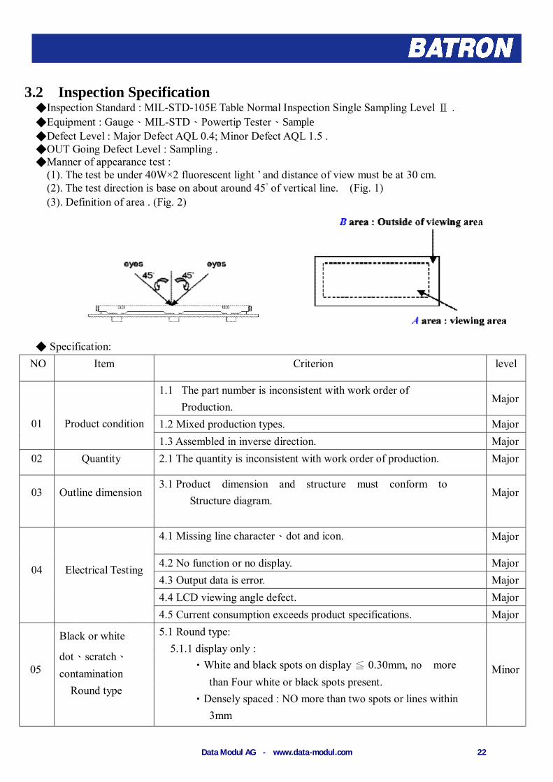
◆Defect Level : Major Defect AQL 0.4; Minor Defect AQL 1.5 . ◆OUT Going Defect Level : Sampling . ◆Manner of appearance test : (1). The test be under 40W×2 fluorescent light ’ and distance of view must be at 30 cm. (2). The test direction is base on about around 45° of vertical line. (Fig. 1) (3). Definition of area . (Fig. 2)
◆ Specification:
NO Item Criterion level
1.1 The part number is inconsistent with work order of Production.
Major
1.2 Mixed production types. Major
01
Product condition 1.3 Assembled in inverse direction. Major
02 Quantity 2.1 The quantity is inconsistent with work order of production. Major
03 Outline dimension 3.1 Product dimension and structure must conform to
Structure diagram. Major
4.1 Missing line character、dot and icon. Major
4.2 No function or no display. Major 4.3 Output data is error. Major 4.4 LCD viewing angle defect. Major
04
Electrical Testing
4.5 Current consumption exceeds product specifications. Major
05
Black or white
dot、scratch、 contamination Round type
5.1 Round type: 5.1.1 display only : •White and black spots on display ≦ 0.30mm, no more than Four white or black spots present. •Densely spaced : NO more than two spots or lines within 3mm
Minor
Data Modul AG - www.data-modul.com 22

◆Specification : NO Item Criterion level 05
Black or white dot、scratch、 contamination Round type
Φ=(x+y)/2
5.1.2 Nom-display :
Dimension (diameter : Φ) Acceptance(Q’ty) Φ≦0.10mm Accept no dense
0.10mm<Φ≦0.20mm 3 0.20mm<Φ≦0.30mm 2
Total 4 5.1.3 Line type:
Dimension (diameter : Φ) Acceptance (Q’ty) Length width A area B area
--- w≦0.03mm Accept no dense Don’t count L≦3.0mm 0.03mm<Φ≦0.05mm Don’t count L≦2.5mm 0.05mm<Φ≦0.075mm
4 Don’t count
--- w>0.075mm As round type
Minor
06
Polarizer Bubble
Acceptance(Q’ty)
Dimension (diameter : Φ) A area B area
Φ≦0.20mm Accept no dense Don’t count 0.20mm<Φ≦0.50mm 3 Don’t count 0.50mm<Φ≦1.00mm 2 Don’t count
Φ>1.00mm 0 Don’t count Total quantity 4 Don’t count
Minor
07
The crack of glass
● Glass Crack: 7.1 Crack on the circuit of electrode terminal :
X Y Z Front X≦1/5 a Y≦ 1/2 D Z≦ t Back Neglect
Minor
Data Modul AG - www.data-modul.com 23

◆Specification : NO Item Criterion Level
● Glass Crack:
7.2 General glass crack and corner edge: 7.2.1
X Y Z Neglect Out A area Neglect
X Y Z Neglect Out A area Neglect
Minor
07
The crack of glass
X: The length of Crack
Y: The width of
crack
Z: The thickness of crack
D: terminal length
T: The thickness of
glass
A : The length of glass
7.3 Glass remain:
X Y Neglect ≦ 1/3 d
Minor
Data Modul AG - www.data-modul.com 24

◆Specification : NO Item Criterion Level 07
The crack of glass
X: The length of Crack
Y: The width of
crack
Z: The thickness of crack
D: terminal length
T: The thickness of
glass
A : The length of glass
7.4 Corner crack and medial crack:
X Y Z
≦1/5a Crack can’t enter viewing area ≦1/2t
≦1/5a Crack can’t exceed the half of
width of SP width of SP 1/2t<Z≦2t
Minor
8.1 Backlight can’t work normally. Major
8.2 Backlight doesn’t light or color is wrong. Major
08
Backlight elements
8.3 Illumination source flickers when lit. Major
9.1 pin type must match type in specification sheet Major
9.2 No short circuits in components on PCB or FPC Major
9.3Product packaging must the same as specified on
packaging specification sheet.
Major
9.4 The folding and peeled off in polarizer are not
acceptable
Major
09
General appearance
9.5 The PCB or FPC between B/L assembled distance
(PCB or FPC) is ≦1.5mm
Major
Data Modul AG - www.data-modul.com 25

4. RELIABILITY TEST 4.1 Reliability Test Condition NO. TEST ITEM TEST CONDITION
1 High Temperature Storage Test Keep in 80 ±2℃ 96 hrs Surrounding temperature, then storage at normal condition 4hrs
2 Low Temperature Storage Test Keep in -30 ±2℃ 96 hrs Surrounding temperature, then storage at normal condition 4hrs
3
High Humidity Storage
Keep in +60℃/90%RH duration for 96 hrs Surrounding temperature, then storage at normal condition 4hrs (Excluding the polarizer)
Air Discharge: Apply 2 KV with 5 times Discharge for each polarity +/-
Contact Discharge: Apply 250V with 5 times discharge for each polarity +/-
4
ESD Test
1. Temperature Ambient:15℃〜35℃ 2. Humidity relative:30%〜60% 3. Energy Storage Capacitance(Cs+Cd):150pF±10% 4. Discharge Resistance(Rd):330Ω±10% 5. Discharge, mode of operation: Single Discharge (time between successive discharges at least 1 s) (Tolerance lf the output voltage indication: ±5%)
5
Temperature Cycling Test
-20℃ → 25℃ → 70℃ → 25℃ (30mins) (5mins) (30mins) (5mins)
10 Cycle Surrounding temperature, then storage at normal condition 4hrs
6
Vibration Test (Packaged)
1. Sine wave 10〜55HZ frequency (1 min) 2. The amplitude of vibration :1.5 mm 3. Each direction (XYZ) duration for 2 Hrs
7
Drop Test (Packaged)
Drop direction :※3 comer /1 edges /6 sides etch 1times
Packing Weight (Kg) Drop Height (cm)
0 ~ 45.4 122
45.4 ~ 90.8 76
90.8 ~ 454 61
Over 454 46
Data Modul AG - www.data-modul.com 26

5. PRECAUTION RELATING PRODUCT HANDLING 5.1 SAFETY
5.1.1 If the LCD panel breaks , be careful not to get the liquid crystal to touch your skin. 5.1.2 If the liquid crystal touches your skin or clothes , please wash it off immediately by
using soap and water. 5.2 HANDLING
5.2.1 Avoid any strong mechanical shock which can break the glass. 5.2.2 Avoid static electricity which can damage the CMOS LSI—When working with the
module , be sure to ground your body and any electrical equipment you may be using. 5.2.3 Do not remove the panel or frame from the module.
5.2.4 The polarizing plate of the display is very fragile. So , please handle it very carefully ,do not touch , push or rub the exposed polarizing with anything harder than an HB pencil lead (glass , tweezers , etc.)
5.2.5 Do not wipe the polarizing plate with a dry cloth , as it may easily scratch the surface of plate.
5.2.6 Do not touch the display area with bare hands , this will stain the display area. 5.2.7 Do not use ketonics solvent & aromatic solvent. Use with a soft cloth soaked with
a cleaning naphtha solvent. 5.2.8 To control temperature and time of soldering is 320±10 and 3℃ -5 sec. 5.2.9 To avoid liquid (include organic solvent) stained on LCM .
5.3 STORAGE 5.3.1 Store the panel or module in a dark place where the temperature is 25 ±5℃ ℃
and the humidity is below 65% RH. 5.3.2 Do not place the module near organics solvents or corrosive gases.
5.3.3 Do not crush , shake , or jolt the module. 5.4 TERMS OF WARRANTY
5.4.1 Applicable warrant period The period is within thirteen months since the date of shipping out under normal using and storage conditions.
5.4.2 Unaccepted responsibility This product has been manufactured to your company’s specification as a part for use in your company’s general electronic products. It is guaranteed to perform according to delivery specifications. For any other use apart from general electronic equipment , we cannot take responsibility if the product is used in nuclear power control equipment , aerospace equipment , fire and security systems or any other applications in which there is a direct risk to human life and where extremely high levels of reliability are required.
Data Modul AG - www.data-modul.com 27


Data Modul Headquarters MunichLandsberger-Str. 322D-80687 Munich - GermanyTel.: +49-89-56017-0
Sales Office DuesseldorfFritz-Vomfelde-Str. 8D-40547 Duesseldorf - GermanyTel.: +49-211-52709-0
Sales Office StuttgartFriedrich-List-Str. 42D-70771 Leinfelden-EchterdingenGermanyTel.: +49-711-782385-0
Data Modul Italia, S.r.l.Regus Center SenigalliaVia Senigallia 18/220161 Milano - ItalyTel.: +39-02-64672-509
Data Modul France, S.A.R.L.Bat B - Hall 2041-3 Rue des Campanules77185 Lognes - FranceTel.: +33-1-60378100
Data Modul Iberia, S.L.c/ Adolfo Pérez Esquivel 3Edificio Las Americas III Oficiana 4028230 Parque EmpresarialMadrid Las Rozas - SpainTel.: +34-916 366 458
Data Modul Inc. / USA275 Marcus Blvd, Unit KHauppauge, NY 11788USATel.: (631)-951-0800
Data Modul Ltd. / UKCollons Building3 Vigo Place - Aldridge - Walsall - WS9 8UGUnited KingdomTel.: +44-121-698-8641
Sales Office HamburgBorsteler Chaussee 51D-22453 Hamburg - GermanyTel.: +49-40-42947377 - 0