section v: analysis and verificationvlsicad.ucsd.edu/publications/aspdac2003_section5-final.pdfjan....
TRANSCRIPT

ASPDAC03 – Physical Chip Implementation – Section V 1
Jan. 2003 ASPDAC03 – Physical Chip Implementation 1
Section V: Analysis and Verification
Jan. 2003 ASPDAC03 - Physical Chip Implementation 2
Overview
Signoff timing verificationPower analysisManufacturability (antennas, OPC, phase-shifting, area fill)Inductance modeling

ASPDAC03 – Physical Chip Implementation – Section V 2
Jan. 2003 ASPDAC03 – Physical Chip Implementation 3
Sign-Off Timing Analysis
Jan. 2003 ASPDAC03 - Physical Chip Implementation 4
Sign-Off Timing Flow Extraction
Extracted wire RC from the layout must be used in Extracted wire RC from the layout must be used in delay calculationsdelay calculationsStatic timing analysis calculates gate and wire delays Static timing analysis calculates gate and wire delays based on the extracted RC and precharacterized gate based on the extracted RC and precharacterized gate attributesattributesThe wire and gate delays are summed, then checked The wire and gate delays are summed, then checked against constraintsagainst constraints
Process and physical effects (such as cross talk) must be account for

ASPDAC03 – Physical Chip Implementation – Section V 3
Jan. 2003 ASPDAC03 - Physical Chip Implementation 5
Setup / Hold
Setup“Does my signal get there before the clock?”“Does my signal get there before the clock?”
Want to measure under the slowest conditionsBad to miss: lower clock speed / lower yield
Hold“Is my signal maintained after the clock?”“Is my signal maintained after the clock?”
Want to measure under the fastest conditionsREALLY bad to miss: chip fails at any frequency
Jan. 2003 ASPDAC03 - Physical Chip Implementation 6
Clocks
SkewDifference between the clock arrival at different Difference between the clock arrival at different flopsflops
Measurable after layoutMust be treated as “uncertainty” during synthesis
UncertaintyPVT variation, characterization inaccuracy, tool PVT variation, characterization inaccuracy, tool inaccuracyinaccuracy

ASPDAC03 – Physical Chip Implementation – Section V 4
Jan. 2003 ASPDAC03 - Physical Chip Implementation 7
Clocks (#2)Jitter
Variance in the clock waveform from cycle to Variance in the clock waveform from cycle to cyclecycle
Effects only setup. Often lumped with uncertainty
Latencydelay from the clock source to the flopdelay from the clock source to the flop
Often set to zero during synthesisUnexpected constraint violations pop up later (clock gating)
Jan. 2003 ASPDAC03 - Physical Chip Implementation 8
ConstraintsConstraints tell the STA tool what to check
Most paths are defined by the clocksMost paths are defined by the clocksOther “exceptions” must be addedOther “exceptions” must be added
false pathsasynchronous clock domains.
Most chips have separate test modes that run at low frequency
Test paths are “false” in functional modeTest paths are “false” in functional modeA separate STA run checks the test timingA separate STA run checks the test timing

ASPDAC03 – Physical Chip Implementation – Section V 5
Jan. 2003 ASPDAC03 - Physical Chip Implementation 9
I/O ConstraintsTypically, half of a chip’s constraints are for I/O
Input signals may be synchronized to an external clock Input signals may be synchronized to an external clock (source synchronous)(source synchronous)An output clock may be come along with output dataAn output clock may be come along with output data
Must be properly aligned
I/O data may come on both edges of a clock (ddr)I/O data may come on both edges of a clock (ddr)Busses on I/O are often constrained to be balancedBusses on I/O are often constrained to be balanced
Jan. 2003 ASPDAC03 - Physical Chip Implementation 10
Special constraints
Clock gating logic also has setup and hold constraints.
Can’t ignore clock latencyCan’t ignore clock latencyNeed a latch/flop to avoid glitches on the gating Need a latch/flop to avoid glitches on the gating signalsignal
PLL feedback paths must be carefully balanced

ASPDAC03 – Physical Chip Implementation – Section V 6
Jan. 2003 ASPDAC03 - Physical Chip Implementation 11
Clock tree
Setup constraint
Clock gating constraint:one cycle to get around – including clock tree latency
Clock Gating Constraint
Jan. 2003 ASPDAC03 - Physical Chip Implementation 12
Timing models
Most of your timing models come from precharacterized “dot lib” filesHard macros may be characterized as
lib fileslib filesFake netlists with overlaid SDFFake netlists with overlaid SDFSynopsys “stamp” modelsSynopsys “stamp” models
You need separate models for slow and fast process conditions.

ASPDAC03 – Physical Chip Implementation – Section V 7
Jan. 2003 ASPDAC03 - Physical Chip Implementation 13
Cross Talk
Cross talk is caused by capacitive coupling between wires
An “aggressor” wire switchesAn “aggressor” wire switchesA “victim” wire is charged or discharged by the A “victim” wire is charged or discharged by the coupling capacitancecoupling capacitance
Jan. 2003 ASPDAC03 - Physical Chip Implementation 14
Cross Talk (glitches)
An otherwise quiet victim may look like it has temporarily switched
This is bad if:This is bad if:The victim is a clock or asynchronous resetThe victim is a signal whose value is being latched at that moment
Fixes:Fixes:Shield/space the wire, use strong drivers, repeater long wires often
ASPDAC03 – Physical Chip Implementation – Section V 8
Jan. 2003 ASPDAC03 - Physical Chip Implementation 15
Aggressor
Victim
Glitch
Jan. 2003 ASPDAC03 - Physical Chip Implementation 16
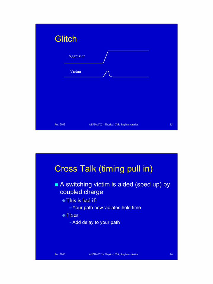
Cross Talk (timing pull in)
A switching victim is aided (sped up) by coupled charge
This is bad if:This is bad if:Your path now violates hold time
Fixes:Fixes:Add delay to your path

ASPDAC03 – Physical Chip Implementation – Section V 9
Jan. 2003 ASPDAC03 - Physical Chip Implementation 17
Aggressor
Victim
Timing Pull-in
Jan. 2003 ASPDAC03 - Physical Chip Implementation 18
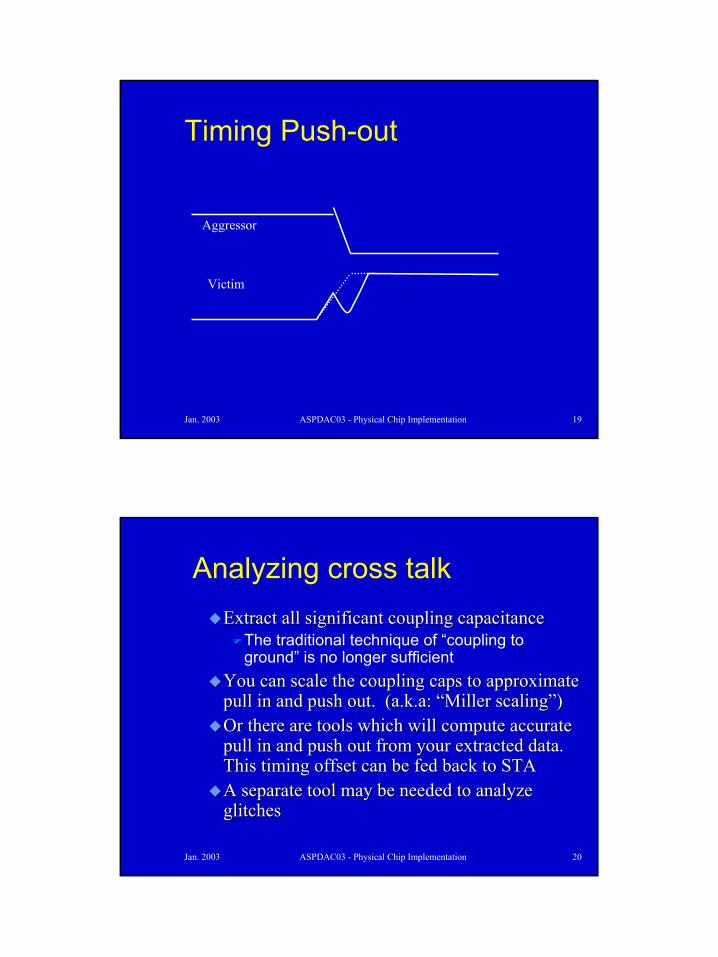
Cross Talk (timing push out)
A switching victim is hindered (slowed down) by coupled charge
This is bad if:This is bad if:Your path now violates setup time
Fixes:Fixes:Space the wires, use strong drivers, add repeaters (to a point)
ASPDAC03 – Physical Chip Implementation – Section V 10
Jan. 2003 ASPDAC03 - Physical Chip Implementation 19
Aggressor
Victim
Timing Push-out
Jan. 2003 ASPDAC03 - Physical Chip Implementation 20
Analyzing cross talkExtract all significant coupling capacitanceExtract all significant coupling capacitance
The traditional technique of “coupling to ground” is no longer sufficient
You can scale the coupling caps to approximate You can scale the coupling caps to approximate pull in and push out. (a.k.a: “Miller scaling”)pull in and push out. (a.k.a: “Miller scaling”)Or there are tools which will compute accurate Or there are tools which will compute accurate pull in and push out from your extracted data. pull in and push out from your extracted data. This timing offset can be fed back to STAThis timing offset can be fed back to STAA separate tool may be needed to analyze A separate tool may be needed to analyze glitchesglitches
ASPDAC03 – Physical Chip Implementation – Section V 11
Jan. 2003 ASPDAC03 - Physical Chip Implementation 21
Timing Windows
Multiple aggressors may affect one victim
If the aggressors switch at the same time, their If the aggressors switch at the same time, their effect is additiveeffect is additiveAn STA tool may produce “timing windows” to An STA tool may produce “timing windows” to tell how the aggressors line uptell how the aggressors line upIf timing windows are not used, all aggressors If timing windows are not used, all aggressors are assumed to come at the same time are assumed to come at the same time (conservative)(conservative)
Jan. 2003 ASPDAC03 - Physical Chip Implementation 22
Timing Windows (#2)
Timing windows are needed for high performance
“Stacking” aggressors for push out is too “Stacking” aggressors for push out is too conservativeconservativeFor pullFor pull--in and glitches, timing windows are in and glitches, timing windows are not necessary The conservatism is generally not necessary The conservatism is generally desired anywaydesired anyway

ASPDAC03 – Physical Chip Implementation – Section V 12
Jan. 2003 ASPDAC03 - Physical Chip Implementation 23
Multiple aggressors with timing windows
Multiple aggressors without timing windows
Effect of Timing Windows
Jan. 2003 ASPDAC03 - Physical Chip Implementation 24
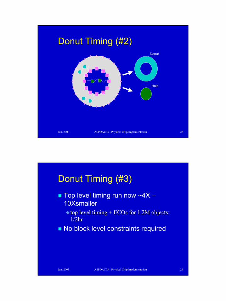
Hierarchical Timing: Donuts
“Donut flow” used for top level timing (and convergence ECO)
split block level netlist into “core” and split block level netlist into “core” and “donut”“donut”split block level parasitics “ “ “ “split block level parasitics “ “ “ “top level netlist + abutment dspf (0 ohm top level netlist + abutment dspf (0 ohm jumpers) connects donut R and Cjumpers) connects donut R and C
ASPDAC03 – Physical Chip Implementation – Section V 13
Jan. 2003 ASPDAC03 - Physical Chip Implementation 25
Donut Timing (#2)Donut
Hole
Jan. 2003 ASPDAC03 - Physical Chip Implementation 26
Donut Timing (#3)
Top level timing run now ~4X –10Xsmaller
top level timing + ECOs for 1.2M objects: top level timing + ECOs for 1.2M objects: 1/2hr1/2hr
No block level constraints required

ASPDAC03 – Physical Chip Implementation – Section V 14
Jan. 2003 ASPDAC03 – Physical Chip Implementation 27
Power Analysis
Jan. 2003 ASPDAC03 - Physical Chip Implementation 28
Power Analysis
Power ConsumptionHow long with the batteries last?How long with the batteries last?How hot will the chip get?How hot will the chip get?
Voltage Drop (IR)Impact on timing, considerable at already low Impact on timing, considerable at already low supply voltages (e.g. 1.5v)supply voltages (e.g. 1.5v)
Electro-Migration (EM)ReliabilityReliability
ASPDAC03 – Physical Chip Implementation – Section V 15
Jan. 2003 ASPDAC03 - Physical Chip Implementation 29
Mars/AstroRail Example
Prepare librariesPrepare filesRun toolsLook at log files, reportsVisually inspect the problem areas
Jan. 2003 ASPDAC03 - Physical Chip Implementation 30
Capacitance Models
.PARA view of blocks, produced with Star-RCXTOr, Apollo LPE (internal extraction engine) if no PARA view (less accurate)LPE needs capacitance models in the technology file, (librarian does this)Without PARA, or LPE, job cannot run

ASPDAC03 – Physical Chip Implementation – Section V 16
Jan. 2003 ASPDAC03 - Physical Chip Implementation 31
Other Avant! Views
Power, PWR views (librarian)TIM (static timing view)CONN view, used during rail analysis and needed for any non-stdcell that contains part of the power distribution network (padcells, covercells)FRAM views (abstracts) with power/ground pins
Jan. 2003 ASPDAC03 - Physical Chip Implementation 32
Net Switching Activity
“number of switches per unit time”Example: if unit is ns, then
4 ns clock = > 2 switches/ 4ns = .5 NS factor4 ns clock = > 2 switches/ 4ns = .5 NS factorSignal switching once every *two* clocks Signal switching once every *two* clocks would be 1 / 2*4 = .125 NS factorwould be 1 / 2*4 = .125 NS factor
In other words:The clock signal switches 2 times per 4 nsThe clock signal switches 2 times per 4 nsThe nonThe non--clock “ “ “ “ 1 time per 8 nsclock “ “ “ “ 1 time per 8 ns

ASPDAC03 – Physical Chip Implementation – Section V 17
Jan. 2003 ASPDAC03 - Physical Chip Implementation 33
Net Switching Activity (#2)
Hence:Clock net switching activity = .5 switches/nsClock net switching activity = .5 switches/nsData net switching activity = .125 switches/nsData net switching activity = .125 switches/ns
Most of the time multiple clocks around, very important to cover all the clocks as the switching factor is much higher.
Jan. 2003 ASPDAC03 - Physical Chip Implementation 34
The Tap File
Specifies the boundary conditions, I.e. the location and layer of the ideal voltage sourcesIR Drop and EM simulations use the information and it must be correct, for example for BGA style pads, the centers of the bumps should be used

ASPDAC03 – Physical Chip Implementation – Section V 18
Jan. 2003 ASPDAC03 - Physical Chip Implementation 35
The Tap File (#2)
The layer of metal and location for the bond-wire attachment point should be used for linear padringsFor a PnR block, the tap file should contain the locations of the power mesh tips at the edge of the block
Jan. 2003 ASPDAC03 - Physical Chip Implementation 36
Power Consumption Summary
Switching powerShort Circuit powerInternal powerLeakage power
ASPDAC03 – Physical Chip Implementation – Section V 19
Jan. 2003 ASPDAC03 - Physical Chip Implementation 37
Switching Power
Power consumed to charge or discharge the capacitive net, which depends on:
Amount of C on the net (from PARA view fo the block, or from LPE based on TLU models)Voltage Supply Value, V (defined by user)Switching Activity, f (defined by user)
= ½ * C * V^2 * f= ½ * C * V^2 * f
Jan. 2003 ASPDAC03 - Physical Chip Implementation 38
Short Circuit Power
Power consumed by current that flows between power net and ground with both pull-up / pull-down logic are temporarily on during switching. Depends on:
Transition time of the input signal (calculated Transition time of the input signal (calculated by running STA)by running STA)
Long nets driven by small drivers will cause long transition times

ASPDAC03 – Physical Chip Implementation – Section V 20
Jan. 2003 ASPDAC03 - Physical Chip Implementation 39
Internal Power / Leakage Power
Internal Power consumed when inputs of a device change but the output does not. Depends on the internal structure of the deviceLeakage power consumed by the current that leaks through the semiconductor junctions. Depends on the physical characteristics of the junctions.
Jan. 2003 ASPDAC03 - Physical Chip Implementation 40
Voltage Drop
Distribution network not ideal, Resistances R, all over the placeCurrent * R = > Voltage dropIf drop too large, noise margins suffer, sensitivity to cross-talk increasesReduces drive strengths, effecting the timing

ASPDAC03 – Physical Chip Implementation – Section V 21
Jan. 2003 ASPDAC03 - Physical Chip Implementation 41
Voltage Drop (#2)For large padring style die, center of chip is the problematic issues (assuming pads are symmetrical, etc)For BGA, life is easy, Max drop a function of distance between pads over the coreGround rails will also have voltage drop: Ground Bounce. Should be similar if distribution networks look the same, but BE CAREFUL and check itTypical targets 5% each for VDD Drop / VSS Bounce.
Jan. 2003 ASPDAC03 - Physical Chip Implementation 42
Electro-MigrationMovement of current in a wire is carried by electrons..too much and metal is damaged. Damage rate proportional to wire cross section and temperature.Two kinds of current flow:
UniUni--directional (power supplies)directional (power supplies)BiBi--directional (signals)directional (signals)
Bi-directional flow has healing effect since atoms are push back and forth, therefore problem not as bad.

ASPDAC03 – Physical Chip Implementation – Section V 22
Jan. 2003 ASPDAC03 - Physical Chip Implementation 43
Electro-Migration (#2)Trends making this problem worse, (.13 copper should help)Dielectric materials between metal layers getting worse for thermal conductivity. Metal self-heading (joule heating) has a harder time being dispersedSignal EM becoming more of an issue (I.e. BUFX20 in .13 require two vias?)
Jan. 2003 ASPDAC03 - Physical Chip Implementation 44
Power: Correct By Construction
Best EM and IR drop solution is robust up-front distribution:
Each power pad has a fixed current capacityEach power pad has a fixed current capacityNumber of power pads initially determined, but Number of power pads initially determined, but as soon as netlist matures tools should be run to as soon as netlist matures tools should be run to calculate preliminary power consumptioncalculate preliminary power consumptionPadring designs must have good power/ground Padring designs must have good power/ground padcell padcell -- to to -- mesh (e.g. ring) interface.mesh (e.g. ring) interface.Too few attachment points create bottlenecksToo few attachment points create bottlenecks

ASPDAC03 – Physical Chip Implementation – Section V 23
Jan. 2003 ASPDAC03 - Physical Chip Implementation 45
Power Bottleneck
Jan. 2003 ASPDAC03 - Physical Chip Implementation 46
Power w/ Improved Ring

ASPDAC03 – Physical Chip Implementation – Section V 24
Jan. 2003 ASPDAC03 – Physical Chip Implementation 47
Manufacturability
Jan. 2003 ASPDAC03 - Physical Chip Implementation 48
Antennas

ASPDAC03 – Physical Chip Implementation – Section V 25
Jan. 2003 ASPDAC03 - Physical Chip Implementation 49
Charging in Semiconductor Processing
Many process steps use plasmas, charged particlesCharge collects on conducting poly, metal surfacesCapacitive coupling: large electrical fields over gate oxidesStresses cause damage or complete breakdownInduced threshold (Vt) shifts affect device matching (e.g., for analog) and timing predictability
Jan. 2003 ASPDAC03 - Physical Chip Implementation 50
Antenna Ratio Limits
Standard solution: limit antenna ratioAntenna ratio = (Apoly + AM1 + …) / Agate-ox
E.g., antenna ratio < 400AMx = metal(x) area that is electrically connected to node without using metal (x+1), and not connected to an active area

ASPDAC03 – Physical Chip Implementation – Section V 26
Jan. 2003 ASPDAC03 - Physical Chip Implementation 51
Antenna Solutions
General solution: bridging (break antenna by moving route to higher layer)
Introduces extra Introduces extra viasvias, congestion, congestionAs antenna ratios get small (and, gate areas decrease rapidly) As antenna ratios get small (and, gate areas decrease rapidly) more bridges are neededmore bridges are needed
Antennas also solved by protection diodesAlso a costly solution: leakage power, area penalties, Also a costly solution: leakage power, area penalties, timing timing penaltiespenalties
Note: Antenna ratio limits of ~400 kill router performance (completion rate, runtime) !
Jan. 2003 ASPDAC03 - Physical Chip Implementation 52
Observations re Antenna RatiosObservation: There should be TWO antenna ratios
One for thickOne for thick--ox (400), one for thinox (400), one for thin--ox (~2000)ox (~2000)Only the more constraining one has been traditionally put into Only the more constraining one has been traditionally put into design rulesdesign rulesThickThick--ox mostly applies to I/O drivers; thinox mostly applies to I/O drivers; thin--ox applies to core ox applies to core
can (safely?) relax the routercan (safely?) relax the router’’s antenna rules by factor of 5x s antenna rules by factor of 5x in corein core
Observation: There should be TWO types of antenna ratios
One is a One is a perper--layerlayer rule, one is a rule, one is a cumulative cumulative ruleruleSometimes perSometimes per--layer rules are put into the design rules, but layer rules are put into the design rules, but they are not as physically meaningful as cumulative rulesthey are not as physically meaningful as cumulative rules

ASPDAC03 – Physical Chip Implementation – Section V 27
Jan. 2003 ASPDAC03 - Physical Chip Implementation 53
OPC and PSM
Jan. 2003 ASPDAC03 - Physical Chip Implementation 54
Subwavelength Optical Lithography — Technology Limits
Implications of Moore's Law for feature sizesSteppers not available; WYSIWYG (layout = mask = wafer) fails after .35µm generationOptical lithography
circuit patterns optically projected onto wafercircuit patterns optically projected onto waferfeature size limited by diffraction effectsfeature size limited by diffraction effectsRayleighRayleigh limitslimits
resolution R proportional to λ / NAdepth of focus DOF proportional to λ / NA2
Available knobsamplitude (aperture): OPCamplitude (aperture): OPCphase: PSMphase: PSM
ASPDAC03 – Physical Chip Implementation – Section V 28
Jan. 2003 ASPDAC03 - Physical Chip Implementation 55
Next-Generation Lithography and the Subwavelength Gap
EUVX-raysE-beamsAll require significant R&D, major infrastructure changes> 30 years of infrastructure and experience supporting optical lithography
Subwavelength Gap since .35 µm
Jan. 2003 ASPDAC03 - Physical Chip Implementation 56
Optical Proximity Correction (OPC)Layout modifications improve process control
improve yield (process latitude)improve yield (process latitude)improve device performanceimprove device performance
With OPCNo OPC
Original Layout(Attenuated PSM)
OPC Corrections

ASPDAC03 – Physical Chip Implementation – Section V 29
Jan. 2003 ASPDAC03 - Physical Chip Implementation 57
Optical Proximity Correction (OPC)Cosmetic corrections; complicates mask manufacturing and dramatically increases costPost-design verification is essential
Rule-based OPCapply corrections based on a set of predetermined rulesfast design time, lower mask complexitysuitable for less aggressive designs
Model-based OPCuse process simulation to determine corrections on-linelonger design time, increased mask complexitysuitable for aggressive designs
Jan. 2003 ASPDAC03 - Physical Chip Implementation 58
OPC FeaturesSerifs - for corner roundingHammerheads - for line-end shorteningGate assists (subresolutionscattering bars) -for CD controlGate biasing - for CDcontrolAffects custom, hierarchical and reuse-based layoutmethodologies

ASPDAC03 – Physical Chip Implementation – Section V 30
Jan. 2003 ASPDAC03 - Physical Chip Implementation 59
OPC IssuesWYSIWYG broken → (mask) verification bottleneckPass functional intent down to OPC insertion
OPC insertion is for predictable circuit performance, functionOPC insertion is for predictable circuit performance, functionMake corrections to win $$$, reduce Make corrections to win $$$, reduce perfperf variation variation costcost--driven RETdriven RET
Pass limits of manufacturing up to layoutdon’t make corrections that can’t be manufactured or verifieddon’t make corrections that can’t be manufactured or verifiedMask Error Enhancement Factor, etc.Mask Error Enhancement Factor, etc.
Layout needs models of OPC insertion processgeometry effects on cost of required OPC to yield functiongeometry effects on cost of required OPC to yield functioncosts of breaking hierarchy (beyond known verification, charactecosts of breaking hierarchy (beyond known verification, characterization rization costs)costs)
Jan. 2003 ASPDAC03 - Physical Chip Implementation 60
Phase Shifting Masksconventional mask
glass
Chrome
phase shifting mask
Phase shifter
0 E at mask 0
0 E at wafer 0
0 I at wafer 0

ASPDAC03 – Physical Chip Implementation – Section V 31
Jan. 2003 ASPDAC03 - Physical Chip Implementation 61
Applicability of OPC and PSM
Jan. 2003 ASPDAC03 - Physical Chip Implementation 62
Double-Exposure Bright-Field PSM
0
180
180 + =
ASPDAC03 – Physical Chip Implementation – Section V 32
Jan. 2003 ASPDAC03 - Physical Chip Implementation 63
180°0°
1. Alternate PSM Mask 2. Trim Mask (COG)
Jan. 2003 ASPDAC03 - Physical Chip Implementation 64
Gate Shrinking and CD Control

ASPDAC03 – Physical Chip Implementation – Section V 33
Jan. 2003 ASPDAC03 - Physical Chip Implementation 65
Phase Assignment ProblemAssign 0, 180 phase regions such that critical features with width (separation) < B are induced by adjacent phase regions with opposite phases
Bright Field AltPSM
0 180
Jan. 2003 ASPDAC03 - Physical Chip Implementation 66
Key: Global 2-Colorability
?180 0
0180 180
180
If there is an odd cycle of “phase implications” → layout cannot be manufactured
layout verification becomes a global, not local, issuelayout verification becomes a global, not local, issue
ASPDAC03 – Physical Chip Implementation – Section V 34
Jan. 2003 ASPDAC03 - Physical Chip Implementation 67
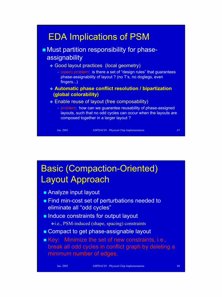
EDA Implications of PSMMust partition responsibility for phase-assignability
Good layout practices (local geometry)Good layout practices (local geometry)(open) problem: is there a set of “design rules” that guarantees phase-assignability of layout ? (no T’s, no doglegs, even fingers...)
Automatic phase conflict resolution / Automatic phase conflict resolution / bipartization bipartization (global (global colorabilitycolorability))Enable reuse of layout (free Enable reuse of layout (free composabilitycomposability))
problem: how can we guarantee reusability of phase-assigned layouts, such that no odd cycles can occur when the layouts are composed together in a larger layout ?
Jan. 2003 ASPDAC03 - Physical Chip Implementation 68
Basic (Compaction-Oriented) Layout Approach
Analyze input layoutFind min-cost set of perturbations needed to eliminate all “odd cycles” Induce constraints for output layout
i.e., PSMi.e., PSM--induced (shape, spacing) constraintsinduced (shape, spacing) constraints
Compact to get phase-assignable layoutKey: Minimize the set of new constraints, i.e., break all odd cycles in conflict graph by deleting a minimum number of edges.

ASPDAC03 – Physical Chip Implementation – Section V 35
Jan. 2003 ASPDAC03 - Physical Chip Implementation 69
Phase-Assignable Layout Flowconflict graph
compaction
phase assignment
find min-cost edge set to be deleted for 2-colorability
Jan. 2003 ASPDAC03 - Physical Chip Implementation 70
PSM Flow IssuesPSM must be “transparent” to ASIC auto-P&R
“free “free composabilitycomposability” is basis of cell” is basis of cell--based methodology!based methodology!focus on poly layer focus on poly layer →→ focus on placer, not routerfocus on placer, not router
Iteration between placer and a separate tool is unacceptableinterface to autointerface to auto--P&R tools is bulky (e.g., 100s of MB for DEF), P&R tools is bulky (e.g., 100s of MB for DEF), slowslowno known convergent method for postno known convergent method for post--P&R phaseP&R phase--assignabilityassignabilitychecks to drive P&R to guaranteed correct solution (very checks to drive P&R to guaranteed correct solution (very difficult!)difficult!)P&R tool MUST deliver guaranteed phase-assignable poly
layer

ASPDAC03 – Physical Chip Implementation – Section V 36
Jan. 2003 ASPDAC03 - Physical Chip Implementation 71
Types of ComposabilitySame-row composability
any cell can be placed immediately adjacent (in the same row) any cell can be placed immediately adjacent (in the same row) to any other cellto any other cell
Adj-row composabilityany cell can be placed in an adjacent cell row to any other cellany cell can be placed in an adjacent cell row to any other cell, , with the two cells having intersecting xwith the two cells having intersecting x--spansspans
Four cases of cell libraries (G = guaranteed; NG = not guaranteed)
Case 1: Case 1: adjadj--G, sameG, same--G G constrained cell layout; transparent to placer
Case 2: Case 2: adjadj--G, sameG, same--NGNGCase 3: Case 3: adjadj--NG, sameNG, same--GGCase 4: Case 4: adjadj--NG, sameNG, same--NGNG
unconstrained cell layout; least transparent to placer
Jan. 2003 ASPDAC03 - Physical Chip Implementation 72
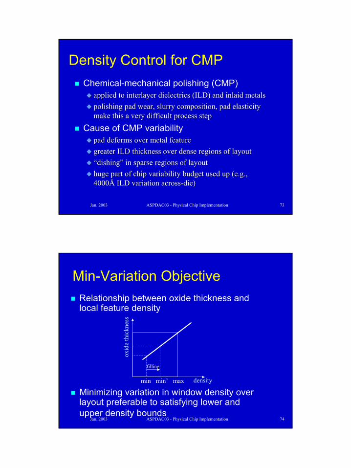
Density Control for CMP
ASPDAC03 – Physical Chip Implementation – Section V 37
Jan. 2003 ASPDAC03 - Physical Chip Implementation 73
Density Control for CMPChemical-mechanical polishing (CMP)
applied to interlayer dielectrics (ILD) and inlaid metalsapplied to interlayer dielectrics (ILD) and inlaid metalspolishing pad wear, slurry composition, pad elasticity polishing pad wear, slurry composition, pad elasticity make this a very difficult process stepmake this a very difficult process step
Cause of CMP variabilitypad deforms over metal featurepad deforms over metal featuregreater ILD thickness over dense regions of layoutgreater ILD thickness over dense regions of layout“dishing” in sparse regions of layout“dishing” in sparse regions of layouthuge part of chip variability budget used up (e.g., huge part of chip variability budget used up (e.g., 4000Å ILD variation across4000Å ILD variation across--die)die)
Jan. 2003 ASPDAC03 - Physical Chip Implementation 74
Min-Variation ObjectiveRelationship between oxide thickness and local feature density
Minimizing variation in window density over layout preferable to satisfying lower and upper density bounds
density
oxid
e th
ickn
ess
filling
min min’ max

ASPDAC03 – Physical Chip Implementation – Section V 38
Jan. 2003 ASPDAC03 - Physical Chip Implementation 75
Damascene, Dual-DamasceneNamed after ancient technique for inlaying metal in ceramic or wood for decoration
• Single Damascene • Dual Damascene
IMD DEP
Oxide Trench Etch
Metal Fill
Metal CMP
Oxide Trench / Via Etch
Metal Fill
Metal CMP
Jan. 2003 ASPDAC03 - Physical Chip Implementation 76
Dual-Damascene Cu ProcessBulk copper removal
Barrier removal
Oxide over-polish
Oxide erosion
Copper dishing
Cu Damascene Process
Polishing pad touches both up and down area after step heightDifferent polish rates on different materialsDishing and erosion arise from different polish rates for copper and oxide

ASPDAC03 – Physical Chip Implementation – Section V 39
Jan. 2003 ASPDAC03 - Physical Chip Implementation
Cu CMP Area Fill / Metal Slot
Dishing can thin the wire or pad, causing higher-resistance wires or lower-reliability bond padsErosion can result in a sub-planar dip on the wafer surface, causing short-circuits between adjacent wires on next layerOxide erosion and copper dishing can be controlled by area filling and metal slotting
Oxide
Copper
Metal SlotArea Fill
Jan. 2003 ASPDAC03 - Physical Chip Implementation 78
Density Control for CMPLayout density control
density rules minimize yield impactdensity rules minimize yield impactuniform density achieved by postuniform density achieved by post--processing, insertion processing, insertion of dummy featuresof dummy features
Performance verification (PV) flow implicationsaccurate estimation of filling is needed in PD, PV tools accurate estimation of filling is needed in PD, PV tools (else broken performance analysis flow)(else broken performance analysis flow)filling geometries affect capacitance extraction by > 50%filling geometries affect capacitance extraction by > 50%is a multilayer problem (coupling to critical nets, is a multilayer problem (coupling to critical nets, contacting restrictions, active layers, other interlayer contacting restrictions, active layers, other interlayer dependencies)dependencies)

ASPDAC03 – Physical Chip Implementation – Section V 40
Jan. 2003 ASPDAC03 - Physical Chip Implementation 79
Density RulesModern foundry rules specify layout density bounds to minimize impact of CMP on yieldDensity rules control local feature density for w ×w windows
e.g., on each metal layer every 200um e.g., on each metal layer every 200um ×× 200um window must 200um window must be between 35% and 70% filledbe between 35% and 70% filled
Filling = insertion of "dummy" features to improve layout density
typically via layout posttypically via layout post--processing in PV / TCAD toolsprocessing in PV / TCAD toolsboolean operations on layout data
affects vital design characteristics (e.g., RC extraction)affects vital design characteristics (e.g., RC extraction)accurate knowledge of filling is required during physical designaccurate knowledge of filling is required during physical designand verification and verification
Jan. 2003 ASPDAC03 - Physical Chip Implementation 80
Need Density-Aware LayoutPerformance verification flow:
Filling/slotting geometries affect RC extraction
RCX ROM DelayCalc
Timing/Noise Analysis
-15
VICTIM LAYER TOTAL CAPACITANCE (10 F)Same layer-i neighbors?
Fill layers i-1, i+1? ε = 3.9 ε = 2.7
N N 2.43 (1.0) 1.68 (1.0) N Y 3.73 (1.54) 2.58 (1.54) Y N 4.47 (1.84) 3.09 (1.84) Y Y 5.29 (2.18) 3.66 (2.18)
Up to 1% error in extracted capacitanceReliability also affected (e.g. slotting of power stripes)

ASPDAC03 – Physical Chip Implementation – Section V 41
Jan. 2003 ASPDAC03 - Physical Chip Implementation 81
Performance verification flow:
Can be considered as ``single-layer’’ problem -15
Middle Victim Conductor Total Capacitance (10 F)
Fill layer offset Fill geometry ε = 3.9 ε = 2.7
N 10 × 1 3.776 (1.0) 2.614 (1.0) N 1 × 1 3.750 (0.99) 2.596 (0.99) Y 10 × 1 3.777 (1.00) 2.615 (1.00) Y 1 × 1 3.745 (0.99) 2.593 (0.99)
• Caveat: contacting, active+gate layers, other layer interactions
RCX ROM DelayCalc
Timing/Noise Analysis
Need Density-Aware Layout
Jan. 2003 ASPDAC03 - Physical Chip Implementation 82
Limitations of Current Density Control Techniques
Current techniques for density control have three key weaknesses:(1) only the average (1) only the average overalloverall feature density is constrained, feature density is constrained,
while local variation in feature density is ignoredwhile local variation in feature density is ignored(2) density analysis does not find (2) density analysis does not find truetrue extremal window extremal window
densities densities -- instead, it finds extremal window densities only instead, it finds extremal window densities only over fixed set of window positions over fixed set of window positions
(3) fill insertion into layout does not minimize the maximum (3) fill insertion into layout does not minimize the maximum variation in window densityvariation in window density
In part, due to PV tool heritage: Boolean operations, inability to touch layout, etc.

ASPDAC03 – Physical Chip Implementation – Section V 42
Jan. 2003 ASPDAC03 - Physical Chip Implementation 83
Layout Density Control FlowDensity Analysis
• find total feature area in each window• find maximum/minimum total feature
area over all w × w windows
Fill synthesis• compute amounts, locations of dummy fill• generate fill geometries
• find slack (available area for filling)in each window
Jan. 2003 ASPDAC03 - Physical Chip Implementation 84
Fixed r-Dissection RegimeFeature area density bounds enforced only for fixed set of w × w windowsLayout partitioned by r2 distinct fixed dissectionsEach w × w window is partitioned in r2 tiles
tile
overlapping windows
fixed r-dissectionwith r = 4
ASPDAC03 – Physical Chip Implementation – Section V 43
Jan. 2003 ASPDAC03 - Physical Chip Implementation 85
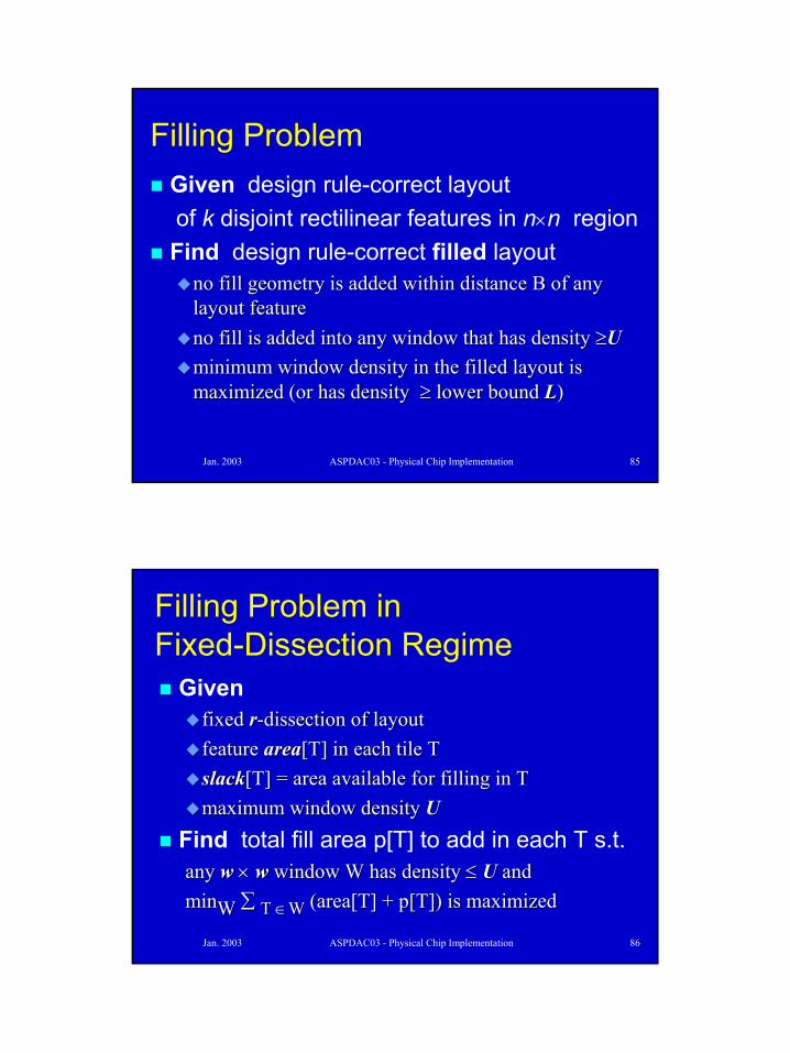
Filling ProblemGiven design rule-correct layout of k disjoint rectilinear features in n×n region Find design rule-correct filled layout
no fill geometry is added within distance B of any no fill geometry is added within distance B of any layout featurelayout featureno fill is added into any window that has density no fill is added into any window that has density ≥≥UUminimum window density in the filled layout is minimum window density in the filled layout is maximized (or has density maximized (or has density ≥≥ lower boundlower bound LL))
Jan. 2003 ASPDAC03 - Physical Chip Implementation 86
Filling Problem in Fixed-Dissection Regime
Givenfixed fixed rr--dissection of layout dissection of layout feature feature areaarea[T] in each tile T[T] in each tile Tslackslack[T] = area available for filling in T[T] = area available for filling in Tmaximum window density maximum window density UU
Find total fill area p[T] to add in each T s.t.any any ww ×× ww window W has density window W has density ≤≤ U U andandminminWW ∑∑ T T ∈∈WW (area[T] + (area[T] + p[T]) p[T]) is maximizedis maximized

ASPDAC03 – Physical Chip Implementation – Section V 44
Jan. 2003 ASPDAC03 - Physical Chip Implementation 87
Fixed-Dissection LP FormulationMaximize M (= lower bound on window density)Subject to:
For any tile T: 0 For any tile T: 0 ≤≤ p[T] p[T] ≤≤ patternpattern ×× slack[T]slack[T]For any window W:For any window W:
∑ T ∈W p[T] + area[T] ≤ U × w2
M ≤ ∑ T ∈W (p[T] + area[T]) (pattern = max achievable pattern area density)
Jan. 2003 ASPDAC03 - Physical Chip Implementation 88
Fixed-Dissection LP Formulation
one variable andtwo constraintsper tile
two constraintsper window

ASPDAC03 – Physical Chip Implementation – Section V 45
Jan. 2003 ASPDAC03 - Physical Chip Implementation 89
Hierarchical Density Control
Hierarchical filling = master cell filling
Tile T Subcells
Features
C1
C2
Cell CSlack[C]
Buffer
Jan. 2003 ASPDAC03 - Physical Chip Implementation 90
Hierarchical LP FormulationFor any cell instance C of master cell C and tile T, γ[C,T] is portion of slack[C] in intersection of C with T:
γ[C,T] = slack(C ∩T)/slack[C]New variable d[C] per each master cell C:
d[C] = filling per master cell CNew constraints:
for total amount of filling added into tile T:for total amount of filling added into tile T:p[T] p[T] = = ∑∑ CC ∩∩TT d[d[CC] ] •• γγ[[CC,T],T]
for amount of filling added into each master cell C:for amount of filling added into each master cell C:0 0 ≤≤ d[d[CC] ] ≤≤ patternpattern ×× slack[slack[CC] ]

ASPDAC03 – Physical Chip Implementation – Section V 46
Jan. 2003 ASPDAC03 - Physical Chip Implementation 91
Synthesis of Filling Patterns
Given area of filling pattern p[i,j], insert filling pattern into tile T[i,j] uniformlyover available area
Desirable properties of filling pattern
uniform coupling to long conductorsuniform coupling to long conductors
either grounded or floatingeither grounded or floating
Jan. 2003 ASPDAC03 - Physical Chip Implementation 92
Basket-Weave Fill Pattern
Each vertical/horizontal crossover line has same overlap capacitance to fill

ASPDAC03 – Physical Chip Implementation – Section V 47
Jan. 2003 ASPDAC03 - Physical Chip Implementation 93
Grounded Fill Pattern
Fill with horizontal stripes,then span with vertical lines
Jan. 2003 ASPDAC03 - Physical Chip Implementation 94
Reticle Reticle Enhancement RoadmapEnhancement Roadmap
Rule-based OPC
Model-based OPC
Scattering Bars
AA-PSM
Weak PSM
Rule-based Tiling
Optimization-driven MB Tiling
0.25 um 0.18 um 0.13 um 0.10 um 0.07 um
248 nm248/193 nm193 nm
Number Of Affected Layers Increases / Generation
Litho
CMP
W. Grobman, Motorola – DAC-2001

ASPDAC03 – Physical Chip Implementation – Section V 48
Jan. 2003 ASPDAC03 - Physical Chip Implementation 95
Optical Lithography Becomes Harder
Numerical Technologies, Inc.
Process window and yield enhancementForbidden widthForbidden width--spacing combinationsspacing combinations (defocus window (defocus window sensitivities)sensitivities)Complex Complex ““local local DRCsDRCs””
Lithography equipment choices (e.g., off-axis illumination)
Forbidden configurationsForbidden configurations (wrong(wrong--way criticalway critical--width doglegs, width doglegs, or diagonal features)or diagonal features)
OPC subresolution assist features (scattering bars)
Notch rules, criticalNotch rules, critical--feature rules on local metalfeature rules on local metal
Jan. 2003 ASPDAC03 - Physical Chip Implementation 96
Many Other Optical Litho Issues
Cell A
Cell A
Cell A
(X1 , Y1)
(X0 , Y0)
(X2 , Y2)
Field-dependentaberrationsaffect the fidelityand placementof critical circuitfeatures.
Big Chip
Example: Field-dependent aberrations cause placement errors and distortions
),(A_CELL),(A_CELL),(A_CELL 220011 YXYXYX ≠≠
Center: Minimal Aberrations
Edge: High Aberrations
Tow
ards
Len
s
Wafer Plane
Lens
R. Pack, Cadence

ASPDAC03 – Physical Chip Implementation – Section V 49
Jan. 2003 ASPDAC03 - Physical Chip Implementation 97
Mask NRE Cost (1999 Sematech)
“$1M mask set” at 100nm, but average only 500 wafers per set
Jan. 2003 ASPDAC03 - Physical Chip Implementation 98
Mask Data and $1M Mask NREMask Data and $1M Mask NREToo many data formats
Most tools have unique data formatMost tools have unique data formatRaster to variable shapedRaster to variable shaped--beam conversion is inefficientbeam conversion is inefficientRealReal--time manufacturing tool switch, time manufacturing tool switch, multiple qualified toolsmultiple qualified toolsduplicate fracturesduplicate fractures to avoid delays if tool switch requiredto avoid delays if tool switch required
Data volumeOPC increases figure count accelerationOPC increases figure count accelerationMEBES format is flatMEBES format is flatALTA machines (mask writers) slow down with > 1GB dataALTA machines (mask writers) slow down with > 1GB dataData volume strains distributed manufacturing resourcesData volume strains distributed manufacturing resources
Refracturing mask data90% of mask data files manipulated or 90% of mask data files manipulated or refracturedrefractured: process bias : process bias sizing (sizing (isoiso--dense, loading effects, linearity, dense, loading effects, linearity, ……), mask write ), mask write optimization, multiple tool formats, optimization, multiple tool formats, ……

ASPDAC03 – Physical Chip Implementation – Section V 50
Jan. 2003 ASPDAC03 - Physical Chip Implementation 99
ContextContext--Dependent FracturingDependent Fracturing
Same pattern, different fractureP. Buck, Dupont Photomasks – ISMT Mask-EDA Workshop July 2001
Jan. 2003 ASPDAC03 - Physical Chip Implementation 100
P. Buck, Dupont Photomasks – ISMT Mask-EDA Workshop July 2001
ITRS Maximum Single Layer File SizeITRS Maximum Single Layer File Size
MEB
ES D
ata
Volu
me
(GB
)
Year

ASPDAC03 – Physical Chip Implementation – Section V 51
Jan. 2003 ASPDAC03 - Physical Chip Implementation 101
ALTAALTA--3500 Mask Write Time3500 Mask Write Time
ABF Data Volume (MB)
Writ
e T i
me
(Ref
o rm
a t +
Prin
t) (H
rs)
P. Buck, Dupont Photomasks – ISMT Mask-EDA Workshop July 2001
Jan. 2003 ASPDAC03 – Physical Chip Implementation 102
Inductance
ASPDAC03 – Physical Chip Implementation – Section V 52
Jan. 2003 ASPDAC03 - Physical Chip Implementation 103
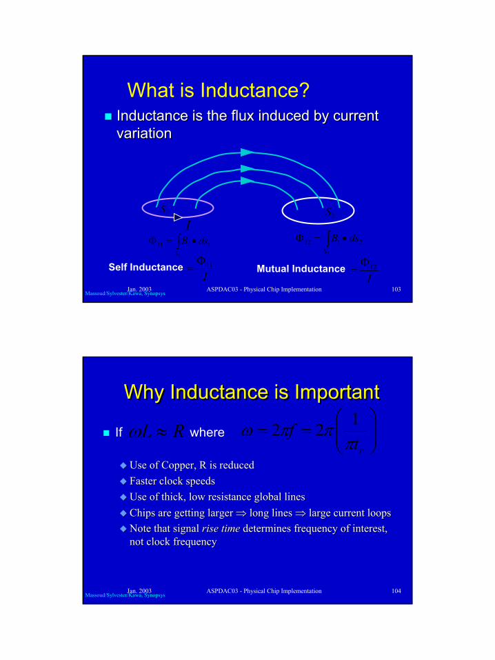
What is Inductance?Inductance is the flux induced by current Inductance is the flux induced by current variationvariation
1S2S
1111
1
dsBS
•=Φ ∫ 2112
2
dsBS
•=Φ ∫I
Self InductanceI11Φ
=I12Φ
=Mutual Inductance
Massoud/Sylvester/Kawa, Synopsys
Jan. 2003 ASPDAC03 - Physical Chip Implementation 104
Why Inductance is ImportantWhy Inductance is Important
If where
Use of Copper, R is reducedUse of Copper, R is reducedFaster clock speedsFaster clock speedsUse of thick, low resistance global linesUse of thick, low resistance global linesChips are getting larger Chips are getting larger ⇒⇒ long lines long lines ⇒⇒ large current loopslarge current loopsNote that signal Note that signal rise timerise time determines frequency of interest, determines frequency of interest, not clock frequencynot clock frequency
RL ≈ω
==
rtf
πππω 122
Massoud/Sylvester/Kawa, Synopsys

ASPDAC03 – Physical Chip Implementation – Section V 53
Jan. 2003 ASPDAC03 - Physical Chip Implementation 105
Edge Rate and Coupling Reach
0 1 2 3 4 5 6 70
10
20
30
40
50
60
70
80
90
100
Inductance
Capacitance
Conductor Distance
Perc
ent o
f Tot
al
Coupling Reach
Fast edge rate ⇒reactance ωL approaches resistanceA resistive wire model may not be sufficiently accurateA resistive wire model may not be sufficiently accurateMutual inductance and resistance become a noise, delay, and Mutual inductance and resistance become a noise, delay, and modeling concernmodeling concern
S. Morton, Compaq
Jan. 2003 ASPDAC03 - Physical Chip Implementation 106
Why Inductance is Important
Line
del
ay
Line length
Fastest slew time
(LC)1/2(RC)/2
Sylvester/Shepard, 2001

ASPDAC03 – Physical Chip Implementation – Section V 54
Jan. 2003 ASPDAC03 - Physical Chip Implementation 107
Why Inductance is ImportantLi
ne d
elay
Line length
Fastest slew time
(LC)1/2(RC)/2
Sylvester/Shepard, 2001
Jan. 2003 ASPDAC03 - Physical Chip Implementation 108
Why Inductance is Important
Line
del
ay
Line length
Fastest slew time
(LC)1/2
(RC)/2
This analysis may require an “effective” inductance that considerssimultaneous switching.
Sylvester/Shepard, 2001
ASPDAC03 – Physical Chip Implementation – Section V 55
Jan. 2003 ASPDAC03 - Physical Chip Implementation 109
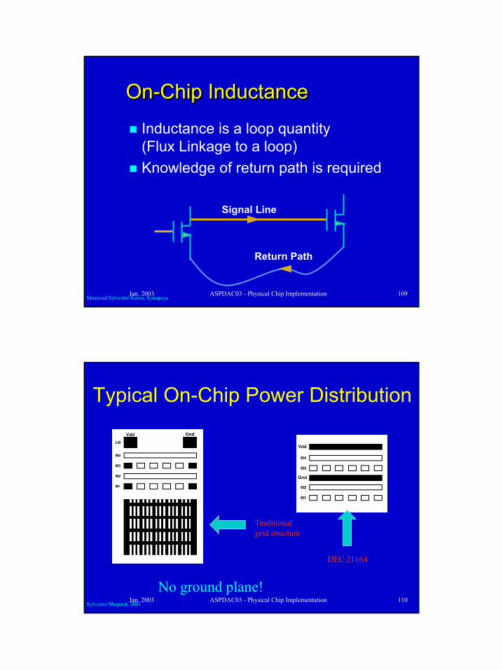
On-Chip Inductance On-Chip Inductance
Inductance is a loop quantity (Flux Linkage to a loop)Knowledge of return path is required
Signal Line
Return Path
Massoud/Sylvester/Kawa, Synopsys
Jan. 2003 ASPDAC03 - Physical Chip Implementation 110
Typical On-Chip Power Distribution
DEC 21164
Traditional grid structure
No ground plane!Sylvester/Shepard, 2001

ASPDAC03 – Physical Chip Implementation – Section V 56
Jan. 2003 ASPDAC03 - Physical Chip Implementation 111
Return Path Hard to DetermineReturn Path Hard to DetermineFrequency dependent return path
At Low Frequency, , current tries toAt Low Frequency, , current tries to
minimize impedance minimize resistanceuse as many returns as possible (parallel resistances)
Signal Gnd Gnd GndGndGndGnd
)( LjR ω+
)( LR ω>>
Massoud/Sylvester/Kawa, Synopsys
Jan. 2003 ASPDAC03 - Physical Chip Implementation 112
Return Path Hard to DetermineReturn Path Hard to DetermineFrequency dependent return path
At High Frequency, At High Frequency, , current tries to, current tries tominimize impedance minimize inductanceuse smallest possible loop (closest return path)
At frequencies where R becomes frequencyAt frequencies where R becomes frequency--dependent, L dominates.dependent, L dominates.At frequencies where L dominates, current returns have “collapseAt frequencies where L dominates, current returns have “collapsed.”d.”Power and ground lines are always available as lowPower and ground lines are always available as low--impedance current impedance current returns at high frequencies.returns at high frequencies.
)( LjR ω+
Signal Gnd Gnd GndGndGndGnd
)( LR ω<<
Massoud/Sylvester/Kawa, Synopsys

ASPDAC03 – Physical Chip Implementation – Section V 57
Jan. 2003 ASPDAC03 - Physical Chip Implementation 113
Loop Impedance: Substrate EffectsLoop Impedance: Substrate Effects
Must provide localized return paths in metal to reduce return resistance and loop impedance
2 GHz2 GHz100 MHz100 MHz
S. Morton, Compaq
Jan. 2003 ASPDAC03 - Physical Chip Implementation 114
Inductance vs. CapacitanceCapacitance
Locality problem easy… electric field lines “suck up” Locality problem easy… electric field lines “suck up” to nearest neighbor conductorsto nearest neighbor conductorsLocal calculation hard… hence all the effort in Local calculation hard… hence all the effort in “accuracy”“accuracy”
InductanceLocality problem hard… magnetic field lines are not Locality problem hard… magnetic field lines are not local; current returns can be complexlocal; current returns can be complexLocal calculation easy… no strong geometry Local calculation easy… no strong geometry dependence… analytic formulae work very well.dependence… analytic formulae work very well.
Sylvester/Shepard, 2001

ASPDAC03 – Physical Chip Implementation – Section V 58
Jan. 2003 ASPDAC03 - Physical Chip Implementation 115
Modeling of Multi-layer, Multi-Conductor Systems
Mut
ual I
nduc
tanc
eM
utua
l Ind
ucta
nce
Mutual Inductance
Capacitance to nearestneighbor is sufficientInductance to distantneighbors is necessaryInductance to wires on other layers is also necessary
Switching activity often Switching activity often unknown!unknown!
S. Morton, Compaq
Jan. 2003 ASPDAC03 - Physical Chip Implementation 116
Signal Integrity Problems Due to Inductance Signal Integrity Problems Due to Inductance
Substrate
S S S S
16 Bit Data Bus
15 Data lines switching simultaneouslyVcc = 5V creates a one volt glitch
Massoud/Sylvester/Kawa, Synopsys
ASPDAC03 – Physical Chip Implementation – Section V 59
Jan. 2003 ASPDAC03 - Physical Chip Implementation 117
EDA Challenges From InductanceHolistic SI/noise management
Inductance effects primarily a noise concernInductance effects primarily a noise concernConventional RC coupling checks can significantly Conventional RC coupling checks can significantly underestimate noiseunderestimate noiseBackBack--end extraction/verification for LRC(f) is costlyend extraction/verification for LRC(f) is costlyNoise estimates may be insufficient if taken without Noise estimates may be insufficient if taken without regard to device, loading, and switching conditions regard to device, loading, and switching conditions
3D RLC accurate/fast extraction is essential to accurately model DSM effectsGlobal busses, clocks, & critical nets must be shielded to minimize coupling effectsTools for 3D analyses of power supply integrity
Signal and supply noise are correlatedSignal and supply noise are correlatedS. Morton, Compaq
Jan. 2003 ASPDAC03 - Physical Chip Implementation 118
Inductance Methodology GoalsSystem to be modeled is very complex
Significant design and simulation timeSignificant design and simulation timeEasy for the inexperienced to get it wrongEasy for the inexperienced to get it wrong
Want methodology to facilitate RC modeling but manage away the inductance:
Various configurations of supply routingVarious configurations of supply routingMultiple wiring lengths, loads, and pitchesMultiple wiring lengths, loads, and pitches
Various distributions of fixed capacitanceVarious combinations of width and spacing
For a range of logic families (static and dynamic)For a range of logic families (static and dynamic)Under worstUnder worst--case conditions (typically fastest case conditions (typically fastest edges)edges)
S. Morton, Compaq

ASPDAC03 – Physical Chip Implementation – Section V 60
Jan. 2003 ASPDAC03 - Physical Chip Implementation 119
Intuition For Interconnect DesignSeesaw effect between inductance and capacitanceMinimize variations in L and C rather than absolutes
Techniques used to minimize variation in capacitive Techniques used to minimize variation in capacitive coupling may also benefit inductive couplingcoupling may also benefit inductive coupling
Employ techniques which reduce net current injection for a given system
S. Morton, Compaq
Jan. 2003 ASPDAC03 - Physical Chip Implementation 120
Useful TechniquesIntroduce shield wires (returns) between signals
Of benefit even for SR ratios beyond 2:1Of benefit even for SR ratios beyond 2:1Required anyway for supply distributionRequired anyway for supply distribution
Introduce reference planes between layersProvides excellent supply performance (low IR, IProvides excellent supply performance (low IR, I22R)R)
Staggered repeater locationsSignaling mechanisms
Complementary logicComplementary logicPredecodedPredecoded signalssignals
+Clat -Clat
+Clat -Clat
Agg
Agg
Vic
S. Morton, Compaq

ASPDAC03 – Physical Chip Implementation – Section V 61
Jan. 2003 ASPDAC03 - Physical Chip Implementation 121
Reduce Coupling by Using Grounded LinesReduce Coupling by Using Grounded Lines
Substrate
AL G AL G
8 Bit Data Bus
Grounding every other line 3x glitch reduction, 2x routing tracks used
Massoud/Sylvester/Kawa, Synopsys
Jan. 2003 ASPDAC03 - Physical Chip Implementation 122
Reduce Area Penalty By Grounding Fewer Lines Reduce Area Penalty By Grounding Fewer Lines
Substrate
AL G AL G
Grounding every third line Factor of 1.5 Reduction Grounding every fourth line Factor of 1.2 Reduction!
8 Bit Data Bus
Massoud/Sylvester/Kawa, Synopsys

ASPDAC03 – Physical Chip Implementation – Section V 62
Jan. 2003 ASPDAC03 - Physical Chip Implementation
Reduce Self Inductance By Shielding
Separation Distance, S [µm]In
duct
ance
[nH
/Cm
]
Sandwiching signal line between ground lines
Keep return path as close as possibleMassoud/Sylvester/Kawa, Synopsys
Jan. 2003 ASPDAC03 - Physical Chip Implementation 124
Regular Structure
“Optimized” Structure W1 = 3µ 3µ
3µ
W2 = 3µ
12µG
GG
C
C1µ1µ
1µ1µ
3µG
L ln(1+ C1/ W1) + C2
L C3 W1 + C4
For small W1 As W1 , L
As W1 , L
≈
≈For large W1
Reduce Self Inductance by Optimizing Signal Line Width
Massoud/Sylvester/Kawa, Synopsys

ASPDAC03 – Physical Chip Implementation – Section V 63
Jan. 2003 ASPDAC03 - Physical Chip Implementation 125
Reduce Self Inductance by Optimizing Signal Line Width
Self
Indu
ctan
ce[n
H/C
m]
Res
ista
nce
[m-O
hm/µ
m]
W1 [µm]
Cap
acita
nce
[fF/µ
m]
W1 [µm]
W1 [µm]Massoud/Sylvester/Kawa, Synopsys
Jan. 2003 ASPDAC03 - Physical Chip Implementation 126
Interdigitate Signal Lines
1µ
C1µ
C1µ
C1µ
G1µ
C
21µ
3 Lines
11 Lines
10µ 3µ3µGG
18µ
C
L2 = L1 / 4 C2 = 1.6 C1 R2= 1.3 R1
1µ
G1µ
G1µ
G1µ
G1µ
C1µ
G
RLω
= 1.07
= 0.20RLω
RLω decreased by a factor of 5.4
rt =100ps
RC analysisMassoud/Sylvester/Kawa, Synopsys

ASPDAC03 – Physical Chip Implementation – Section V 64
Jan. 2003 ASPDAC03 - Physical Chip Implementation 127
Dedicated Ground Planes
Dedicated Ground Planes
Dedicated G.P.C
G
G
W1
WgMassoud/Sylvester/Kawa, Synopsys
Jan. 2003 ASPDAC03 - Physical Chip Implementation 128
Guard Traces vs. Dedicated Ground Planes
Below 5 GHz, guard traces are betterFrequency [Hz]
Indu
ctan
ce[n
H/C
m] Dedicated G.P.
Guard Traces
Massoud/Sylvester/Kawa, Synopsys

ASPDAC03 – Physical Chip Implementation – Section V 65
Jan. 2003 ASPDAC03 - Physical Chip Implementation 129
LF Current Distribution Top View
Current spreads through outer, bigger current loops
Current Flow in Dedicated G.P.
Current Flow in Guard Traces
Smaller Current Loops
Smaller Inductance
Massoud/Sylvester/Kawa, Synopsys
Jan. 2003 ASPDAC03 - Physical Chip Implementation 130
HF Current Distribution Top View
Current Flow in Guard Traces
Current concentrates underneath signal line Much smaller current loops, and smaller inductance
Current Flow in Dedicated G.P.
Massoud/Sylvester/Kawa, Synopsys

ASPDAC03 – Physical Chip Implementation – Section V 66
Jan. 2003 ASPDAC03 - Physical Chip Implementation 131
Extraction: Partial Inductance and Return-Limited Inductance
B BVDD/GNDCurrent return at infinity.
Sylvester/Shepard, 2001
Jan. 2003 ASPDAC03 - Physical Chip Implementation 132
Return-Limited Inductance ExtractionNeed to determine which mutual inductances to discard and wish to use the power-ground network as an “always-available” current return.To do this, we:
Use the powerUse the power--ground distribution to divide the interconnect into disjoint ground distribution to divide the interconnect into disjoint interaction regions. Mutual inductances between interaction reginteraction regions. Mutual inductances between interaction regions are ions are discarded.discarded.PowerPower--ground wires within the interaction region act as a “distributedground wires within the interaction region act as a “distributedground plane”.ground plane”.
A set of geometry-based matrix decomposition rules guide the interaction region definition (halo rules).
Sylvester/Shepard, 2001
ASPDAC03 – Physical Chip Implementation – Section V 67
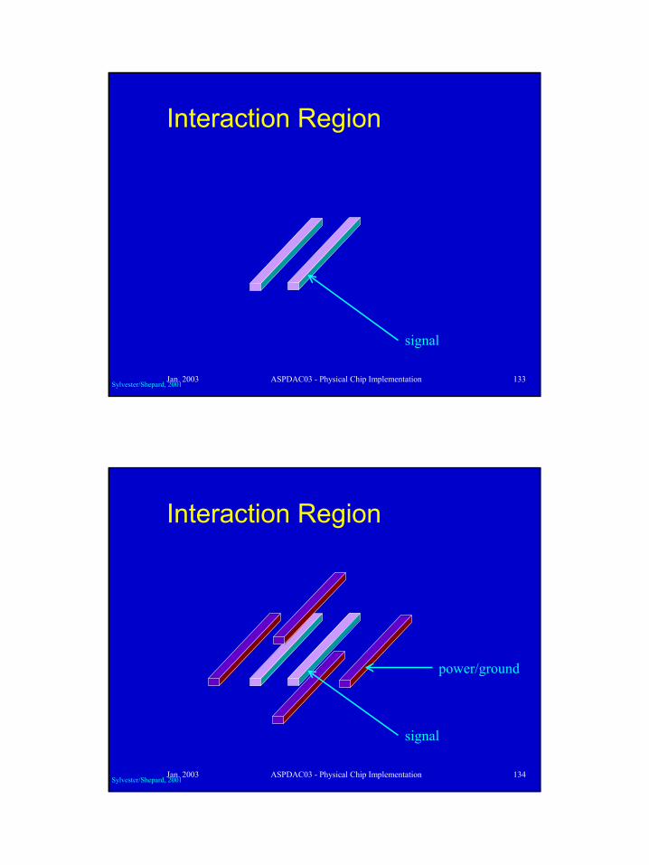
Jan. 2003 ASPDAC03 - Physical Chip Implementation 133
Interaction Region
signal
Sylvester/Shepard, 2001
Jan. 2003 ASPDAC03 - Physical Chip Implementation 134
Interaction Region
power/ground
signal
Sylvester/Shepard, 2001

ASPDAC03 – Physical Chip Implementation – Section V 68
Jan. 2003 ASPDAC03 - Physical Chip Implementation 135
Interaction Region
power/ground
signal
interaction region
Sylvester/Shepard, 2001
Jan. 2003 ASPDAC03 - Physical Chip Implementation 136
Interaction Region
power/ground
signal
interaction region
Sylvester/Shepard, 2001

ASPDAC03 – Physical Chip Implementation – Section V 69
Jan. 2003 ASPDAC03 - Physical Chip Implementation 137
Assura RLCX Architecture
LVS
GDSII
Edge file Device files
Resistance extraction (rex)
Edge file with resistor cuts
Resistance files
Capacitance extraction
Capacitance file
Spice netlist generator
Spice files
lextract
Interaction region file
regcal
Microinductance file
wirecal
Inductance file
Sylvester/Shepard, 2001