see testing of advanced memories - part 1
TRANSCRIPT
D/TEC-QCA Final Presentation Day 200724/01/2007
SEE testing of Advanced Memories - Part 1
Test approach and hardware evolution from SDRAM to DDR2
Sample preparation
This work has been performed under ESTEC Contract No. 13528/99/NL/MV, COO-19
FX. GUERREG. LEWIS
HIREX EngineeringToulouse - France
D/TEC-QCA Final Presentation Day 200724/01/2007 2/20
SEE Testing of Advanced Memories - Part 1
FX. GUERREG. LEWIS
PlanWork contextOverview of DRAM technologiesSEE test approach of SDRAM, DDR and DDR2Application to SDRAM Evolution to DDR2 SDRAMSample preparation
D/TEC-QCA Final Presentation Day 200724/01/2007 3/20
SEE Testing of Advanced Memories - Part 1
FX. GUERREG. LEWIS
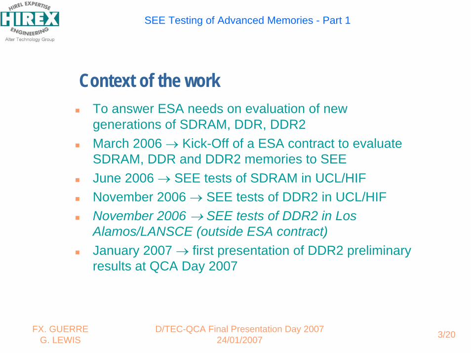
Context of the workTo answer ESA needs on evaluation of new generations of SDRAM, DDR, DDR2March 2006 → Kick-Off of a ESA contract to evaluate SDRAM, DDR and DDR2 memories to SEEJune 2006 → SEE tests of SDRAM in UCL/HIFNovember 2006 → SEE tests of DDR2 in UCL/HIFNovember 2006 → SEE tests of DDR2 in Los Alamos/LANSCE (outside ESA contract)January 2007 → first presentation of DDR2 preliminary results at QCA Day 2007
D/TEC-QCA Final Presentation Day 200724/01/2007 4/20
SEE Testing of Advanced Memories - Part 1
FX. GUERREG. LEWIS
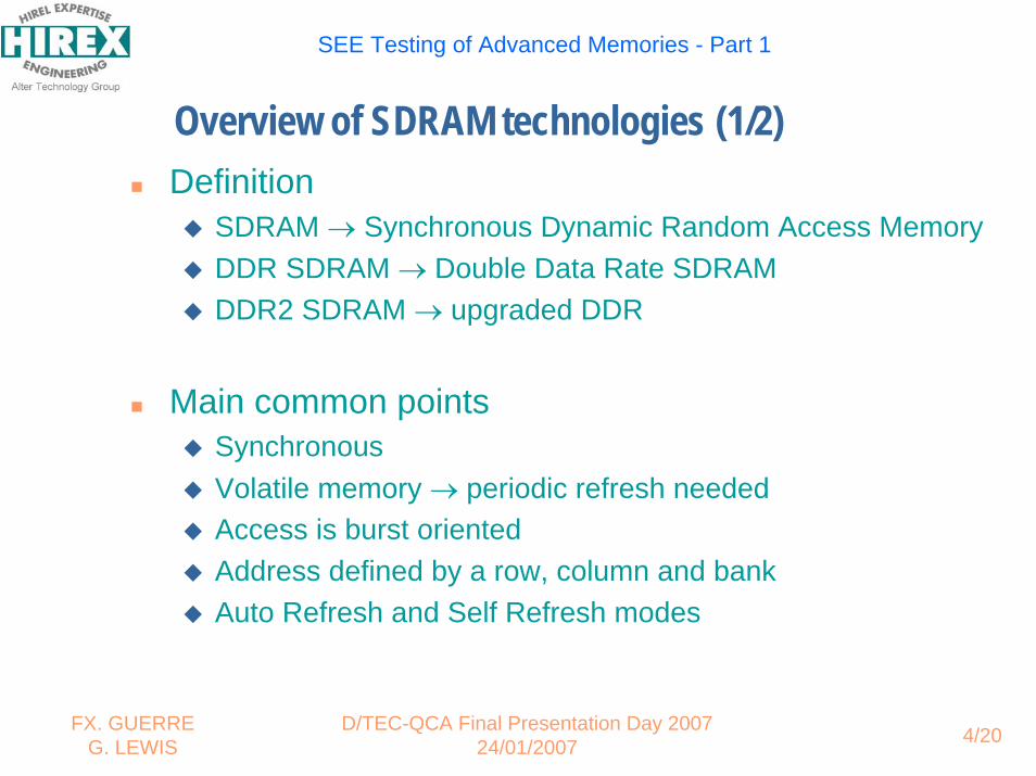
Overview of SDRAM technologies (1/2)Definition
SDRAM → Synchronous Dynamic Random Access MemoryDDR SDRAM → Double Data Rate SDRAMDDR2 SDRAM → upgraded DDR
Main common pointsSynchronousVolatile memory → periodic refresh neededAccess is burst orientedAddress defined by a row, column and bankAuto Refresh and Self Refresh modes

D/TEC-QCA Final Presentation Day 200724/01/2007 5/20
SEE Testing of Advanced Memories - Part 1
FX. GUERREG. LEWIS
Overview of SDRAM technologies (2/2)Main differences
3.3VTSOP package133 MHz max
2.5VTSOP and FBGA packages90 MHz min, 200 MHz max*Differential signals
1.8VFBGA package125 MHz min, 333 MHz max*Differential signals
+ data rates, capacities increased... due to new generations

D/TEC-QCA Final Presentation Day 200724/01/2007 6/20
SEE Testing of Advanced Memories - Part 1
FX. GUERREG. LEWIS
Interests of new generations of SDRAM for space applicationsObsolescence
Capacity, data rateConsumption
Source: Micron website
D/TEC-QCA Final Presentation Day 200724/01/2007 7/20
SEE Testing of Advanced Memories - Part 1
FX. GUERREG. LEWIS
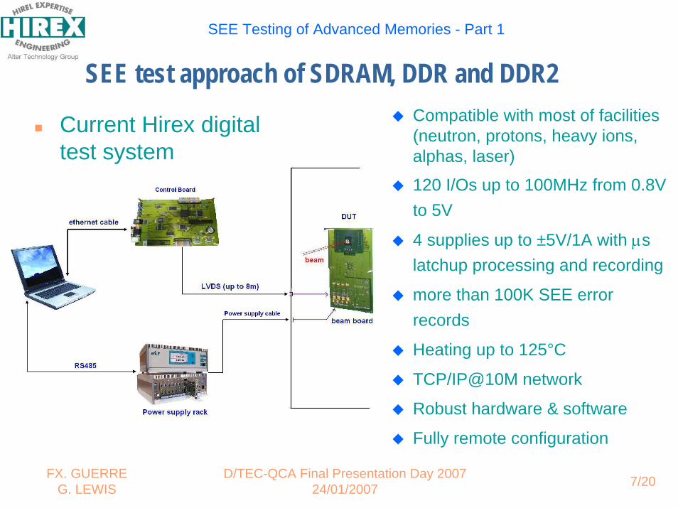
SEE test approach of SDRAM, DDR and DDR2
Current Hirex digital test system
Compatible with most of facilities (neutron, protons, heavy ions, alphas, laser)
120 I/Os up to 100MHz from 0.8V to 5V
4 supplies up to ±5V/1A with µs latchup processing and recording
more than 100K SEE error records
Heating up to 125°C
TCP/IP@10M network
Robust hardware & software
Fully remote configuration
D/TEC-QCA Final Presentation Day 200724/01/2007 8/20
SEE Testing of Advanced Memories - Part 1
FX. GUERREG. LEWIS
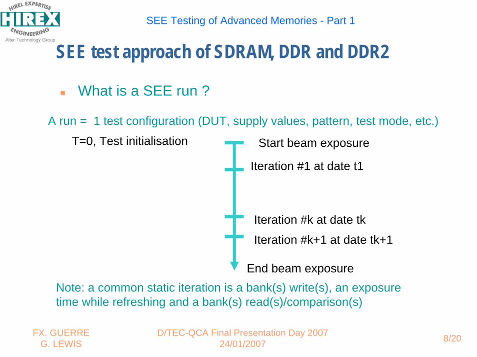
SEE test approach of SDRAM, DDR and DDR2
What is a SEE run ?
A run = 1 test configuration (DUT, supply values, pattern, test mode, etc.)
Iteration #k at date tk
Iteration #k+1 at date tk+1
T=0, Test initialisation Start beam exposure
End beam exposure
Iteration #1 at date t1
Note: a common static iteration is a bank(s) write(s), an exposure time while refreshing and a bank(s) read(s)/comparison(s)
D/TEC-QCA Final Presentation Day 200724/01/2007 9/20
SEE Testing of Advanced Memories - Part 1
FX. GUERREG. LEWIS
SEE test approach of SDRAM, DDR and DDR2
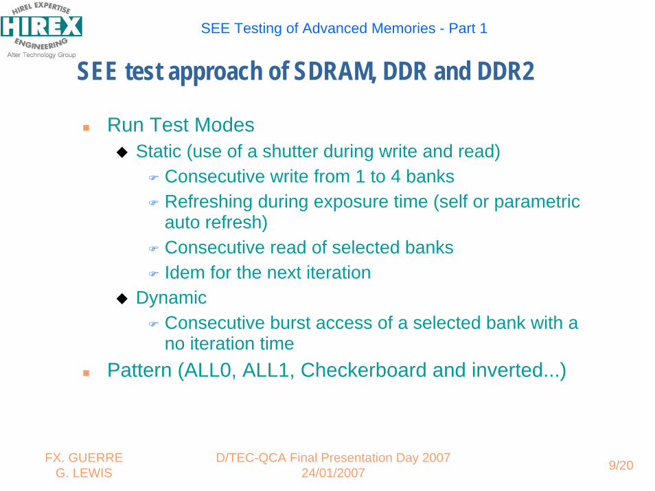
Run Test ModesStatic (use of a shutter during write and read)
Consecutive write from 1 to 4 banksRefreshing during exposure time (self or parametric auto refresh)Consecutive read of selected banksIdem for the next iteration
DynamicConsecutive burst access of a selected bank with a no iteration time
Pattern (ALL0, ALL1, Checkerboard and inverted...)
D/TEC-QCA Final Presentation Day 200724/01/2007 10/20
SEE Testing of Advanced Memories - Part 1
FX. GUERREG. LEWIS
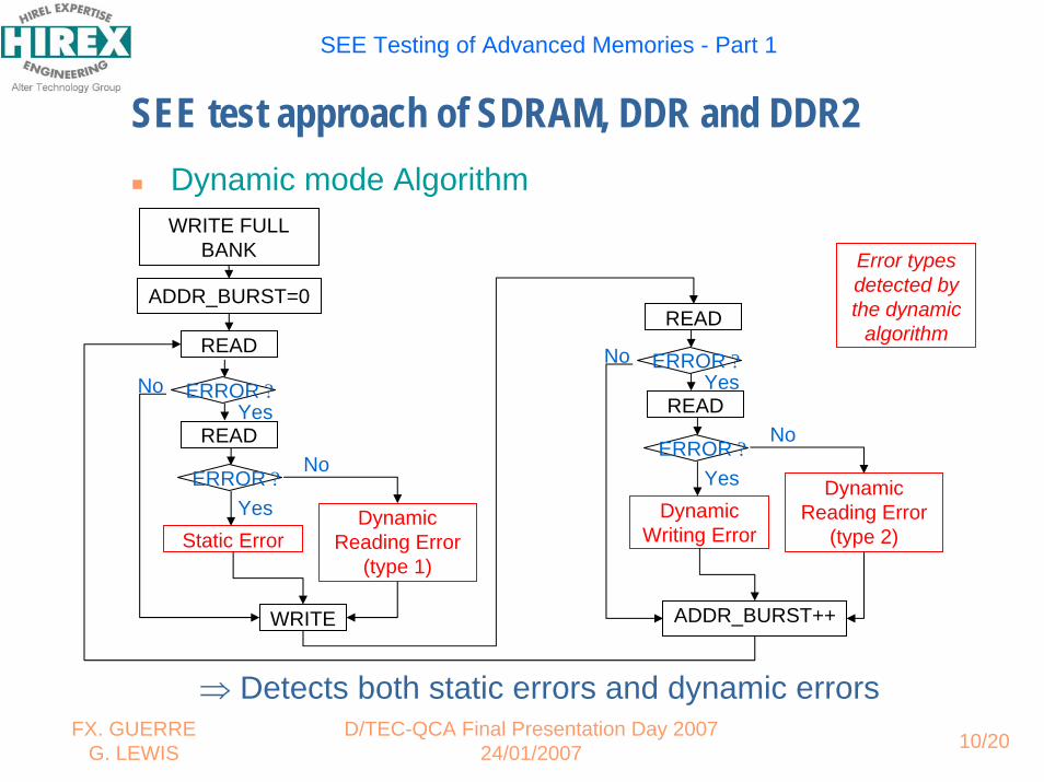
SEE test approach of SDRAM, DDR and DDR2Dynamic mode Algorithm
Error types detected by the dynamic
algorithm
WRITE FULL BANK
READ
No
WRITE
Static ErrorDynamic
Reading Error (type 1)
ADDR_BURST=0
READ
ERROR ?
ERROR ?
NoYes
Yes
READ
No
Dynamic Writing Error
Dynamic Reading Error
(type 2)
READ
ERROR ?
ERROR ?
NoYes
Yes
ADDR_BURST++
⇒ Detects both static errors and dynamic errors
D/TEC-QCA Final Presentation Day 200724/01/2007 11/20
SEE Testing of Advanced Memories - Part 1
FX. GUERREG. LEWIS
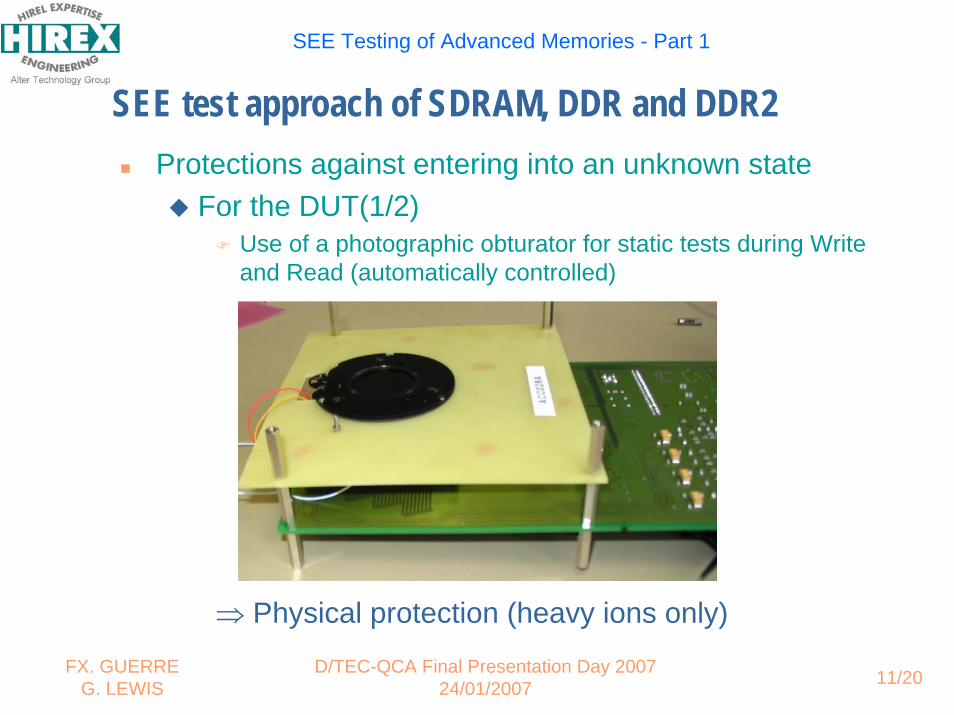
SEE test approach of SDRAM, DDR and DDR2Protections against entering into an unknown state
For the DUT(1/2)Use of a photographic obturator for static tests during Write and Read (automatically controlled)
⇒ Physical protection (heavy ions only)
D/TEC-QCA Final Presentation Day 200724/01/2007 12/20
SEE Testing of Advanced Memories - Part 1
FX. GUERREG. LEWIS
SEE test approach of SDRAM, DDR and DDR2Protections against entering into an unknown state
For the DUT(2/2)Automatic detection of unknown state during read
• Reload of the memory registers• Reread of the memory without rewriting it
– if unknown state can be recovered by software →Count a “Soft SEFI”
– if unknown state can only be recovered by power off the DUT (automatic power OFF and re-power ON) →Count a “Hard SEFI”
For the control circuitry under harsh environment (protons, neutrons)
Periodic reload of the FPGA which drives the memory
⇒ Software protections
D/TEC-QCA Final Presentation Day 200724/01/2007 13/20
SEE Testing of Advanced Memories - Part 1
FX. GUERREG. LEWIS
SEE test approach of SDRAM, DDR and DDR2
Detected errors typesSEU: Single Bit errorMCU: Multi Cell Error (scrambling info needed)MBU: Multi Bit Error (in the same word)Row/Column errorRead errors, Write errors, Cell errorsSoft SEFI (registers modification possible)Hard SEFI (when power reset is needed)SEL

D/TEC-QCA Final Presentation Day 200724/01/2007 14/20
SEE Testing of Advanced Memories - Part 1
FX. GUERREG. LEWIS
Application to SDRAM and DDR2SDRAM
Current Hirex test system based on a Xilinx FPGA Virtex2
DDR2Current Hirex test system+ one additional board based on a Xilinx FPGA Virtex4

D/TEC-QCA Final Presentation Day 200724/01/2007 15/20
SEE Testing of Advanced Memories - Part 1
FX. GUERREG. LEWIS
Performances of the test systems
Test SEE of SDRAM DDR2 DDR2 DDR2
Campaign UCL - June 2006
UCL - Nov. 2006
Los Alamos - Nov. 2006
Expected in 2007
Frequency 25 MHz 166 MHz 200 MHz 200 MHz % accessing
time - ~30% ~25% ~50%
D/TEC-QCA Final Presentation Day 200724/01/2007 16/20
SEE Testing of Advanced Memories - Part 1
FX. GUERREG. LEWIS
Sample preparation
Using Hirex Physical Analysis Lab resources (equipped for Construction Analysis, DPA, Failure analysis)Preparation of SDRAM/DDR2 memories for heavy ions radiation testing:
Chemical etching (jet etcher)
Die thinning (ASAP1 / mechanical lapping)
D/TEC-QCA Final Presentation Day 200724/01/2007 17/20
SEE Testing of Advanced Memories - Part 1
FX. GUERREG. LEWIS
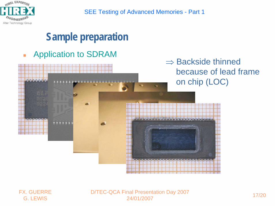
Sample preparationApplication to SDRAM
⇒ Backside thinned because of lead frame on chip (LOC)
D/TEC-QCA Final Presentation Day 200724/01/2007 18/20
SEE Testing of Advanced Memories - Part 1
FX. GUERREG. LEWIS
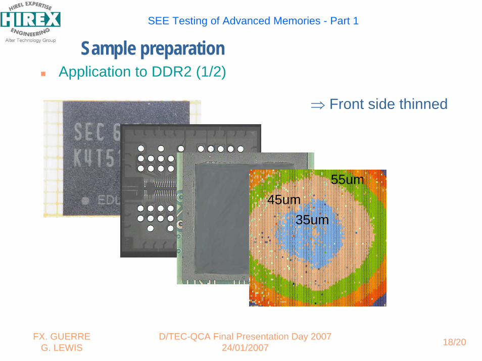
Sample preparationApplication to DDR2 (1/2)
⇒ Front side thinned
35um45um
55um

D/TEC-QCA Final Presentation Day 200724/01/2007 19/20
SEE Testing of Advanced Memories - Part 1
FX. GUERREG. LEWIS
Sample preparation
Application to DDR2 (2/2)
Balls
Board
Lead frame printed on glass
fiber sheetDie
Chip
Bonding
D/TEC-QCA Final Presentation Day 200724/01/2007 20/20
SEE Testing of Advanced Memories - Part 1
FX. GUERREG. LEWIS
ConclusionAchievements
SEE tests of 3 SDRAM and 2 DDR2 (heavy ions and neutrons)⇒ First results for DDR2. See « SEE testing of Synchronous Dynamic RAM - Part 2 » presentation
Conception and validation of a prototype for an upgraded test system
⇒ Allow SEE tests of new generations of advanced memories (DDR2 up to 400Mb/s, RLDRAM, QDRAM...)
Validation of the different error detection and process (Soft SEFI, Hard SEFI...)
NextDesign and production of improved ASERT test board (4 power supplies, 488 I/Os, up to 500 MHz for FPGA clock speed...)In depth radiations tests on different DDR2 memories