semiconductor detectors @ lal nicoleta dinu
TRANSCRIPT

N. D
inu,
LA
L-O
rsay
, Rés
eau
sem
i-co
nduc
teur
s IN
2P3,
21.
10.2
014
1
Semiconductor detectors @ LAL
Nicoleta Dinu
Laboratoire de l’Accélérateur Linéaire, Orsay

N. D
inu,
LA
L-O
rsay
, Rés
eau
sem
i-co
nduc
teur
s IN
2P3,
21.
10.2
014
2
Outline
• Silicon planar pixel sensors – High energy physics - ATLAS @ HL-LHC
• Diamond sensors – Accelerator physics - ATF2
• Silicon Photomultiplier sensors (SiPM) – Tool for semiconductor physics (i.e. avalanche, defects)
– Applications: • Medical imaging
• High energy physics

N. D
inu,
LA
L-O
rsay
, Rés
eau
sem
i-co
nduc
teur
s IN
2P3,
21.
10.2
014
3 Slide by A. Lounis

N. D
inu,
LA
L-O
rsay
, Rés
eau
sem
i-co
nduc
teur
s IN
2P3,
21.
10.2
014
4
Experimental tools for sensors characterization (1)
New clean-room at LAL, class 10000, 100 m2
equipped with a semi-automatic probe-station
(R. Cornat, P2IO – CAPTINOV project)
Old ATLAS clean-room – class 100000, 12 m2

N. D
inu,
LA
L-O
rsay
, Rés
eau
sem
i-co
nduc
teur
s IN
2P3,
21.
10.2
014
5 5 5
Experimental tools for sensors characterization (2)
SIMS at GEMaC laboratory, Versailles
Cameca IMS 7F AFM at CTU-Minerve, IEF, Orsay
Collaborations with GEMAC and CTU-IEF laboratories for doping profiles characterizations

N. D
inu,
LA
L-O
rsay
, Rés
eau
sem
i-co
nduc
teur
s IN
2P3,
21.
10.2
014
6
SYNOPSYS TCAD simulations
Comparison: SIMS measurements/ SYNOPSYS simulations
• very promising results
SIMS: N. Dinu, F. Jomard
SYNOPSIS simulations: V. Gkougkousis
(TIPDOC project, Labex NanoSaclay, data not yet published)

N. D
inu,
LA
L-O
rsay
, Rés
eau
sem
i-co
nduc
teur
s IN
2P3,
21.
10.2
014
Diamond sensor R&D for
Beam Halo investigation
Tests in the clean room to study the diamond characteristics
Tested in air at PHIL from 105 ->108 e-
Tests to be continued in vacuum
Installation at ATF2 for beam halo measurements in Nov. 2014
Slides by S. Liu

N. D
inu,
LA
L-O
rsay
, Rés
eau
sem
i-co
nduc
teur
s IN
2P3,
21.
10.2
014
8
- SiPM for medical imaging

N. D
inu,
LA
L-O
rsay
, Rés
eau
sem
i-co
nduc
teur
s IN
2P3,
21.
10.2
014
9

N. D
inu,
LA
L-O
rsay
, Rés
eau
sem
i-co
nduc
teur
s IN
2P3,
21.
10.2
014
10

N. D
inu,
LA
L-O
rsay
, Rés
eau
sem
i-co
nduc
teur
s IN
2P3,
21.
10.2
014
11
N. D
inu,
LA
L-O
rsay
, Rés
eau
sem
i-co
nduc
teur
s IN
2P3,
21.
10.2
014
12
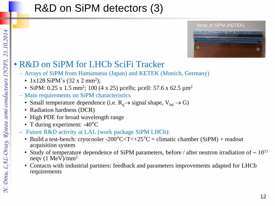
• R&D on SiPM for LHCb SciFi Tracker – Arrays of SiPM from Hamamatsu (Japan) and KETEK (Munich, Germany)
• 1x128 SiPM’s (32 x 2 mm2);
• SiPM: 0.25 x 1.5 mm2; 100 (4 x 25) µcells; µcell: 57.6 x 62.5 µm2
– Main requirements on SiPM characteristics
• Small temperature dependence (i.e. Rq signal shape, Vbd G)
• Radiation hardness (DCR)
• High PDE for broad wavelength range
• T during experiment: -40°C
– Future R&D activity at LAL (work package SiPM LHCb):
• Build a test-bench: cryocooler -200°C<T<+25°C + climatic chamber (SiPM) + readout acquisition system
• Study of temperature dependence of SiPM parameters, before / after neutron irradiation of 1011 neqv (1 MeV)/mm2
• Contacts with industrial partners: feedback and parameters improvements adapted for LHCb requirements
Array of SiPM (KETEK)
R&D on SiPM detectors (3)
N. D
inu,
LA
L-O
rsay
, Rés
eau
sem
i-co
nduc
teur
s IN
2P3,
21.
10.2
014
13 13
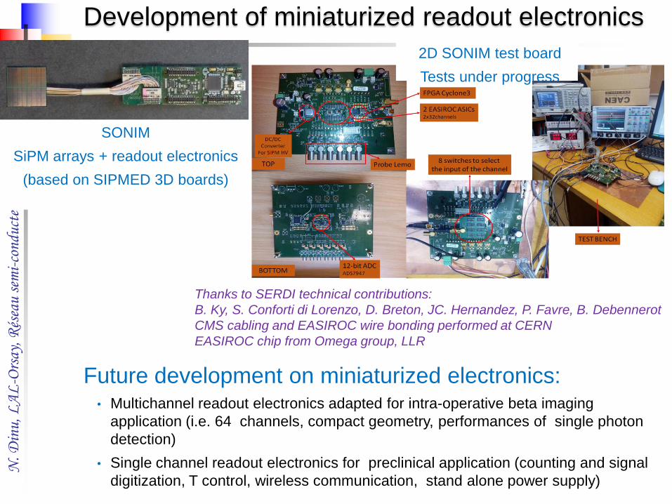
Development of miniaturized readout electronics
Thanks to SERDI technical contributions:
B. Ky, S. Conforti di Lorenzo, D. Breton, JC. Hernandez, P. Favre, B. Debennerot
CMS cabling and EASIROC wire bonding performed at CERN
EASIROC chip from Omega group, LLR
2D SONIM test board
Tests under progress
Future development on miniaturized electronics: • Multichannel readout electronics adapted for intra-operative beta imaging
application (i.e. 64 channels, compact geometry, performances of single photon
detection)
• Single channel readout electronics for preclinical application (counting and signal
digitization, T control, wireless communication, stand alone power supply)
SONIM
SiPM arrays + readout electronics
(based on SIPMED 3D boards)