sepic analysis
TRANSCRIPT

Power Systems Design Europe November 200614
DESIGN TIPS
By Dr. Ray Ridley, Ridley Engineering
The Sepic ConverterThe most basic converter that we
looked at last month is the buck con-verter. It is so named because it always steps down, or bucks, the input voltage. The output of the converter is given by:
Interchange the input and the output of the buck converter, and you get the second basic converter – the boost. The boost always steps up, hence its name. The output voltage is always higher than the input voltage, and is given by:
What if you have an application where you need to both step up and step down, depending on the input and output voltage? You could use two cas-caded converters – a buck and a boost. Unfortunately, this requires two separate controllers and switches. It is, however, a good solution in many cases.
The buck-boost converter has the de-sired step up and step down functions:
The output is inverted. A flyback convert-er (isolated buck-boost) requires a trans-former instead of just an inductor, adding to the complexity of the development.
One converter that provides the need-ed input-to-output gain is the Sepic (sin-gle-ended primary inductor converter) converter. A Sepic converter is shown in Fig. 1. It has become popular in recent
years in battery-powered systems that must step up or down depending upon the charge level of the battery.
Fig. 2 shows the circuit when the power switch is turned on. The first inductor, L1, is charged from the input voltage source during this time. The second inductor takes energy from the first capacitor, and the output capacitor is left to provide the load current. The fact that both L1 and L2 are disconnect-ed from the load when the switch is on leads to complex control characteristics, as we will see later.
When the power switch is turned off, the first inductor charges the capaci-tor C1 and also provides current to the load, as shown in Fig. 3. The second inductor is also connected to the load during this time.
The output capacitor sees a pulse of current during the off time, making it inherently noisier than a buck converter.
The input current is non-pulsating, a dis-tinct advantage in running from a battery supply.
Analyzing the Sepic Converter
In the last issue, we talked about the simplest of all converters, the buck converter, and showed how
its control transfer functions could be extraordinarily complex. In this issue, we’ll go to the other end of
the spectrum, and look at a converter that is far more complex, yet is often used by engineers who are
unaware of the difficulties that follow.
Figure 1. The Sepic converter can both step up and step down the input volt-age, while maintaining the same polar-ity and the same ground reference for the input and output.
Figure 2. When the switch is turned on, the input inductor is charged from the source, and the second inductor is charged from the first capacitor. No energy is supplied to the load capaci-tor during this time. Inductor current and capacitor voltage polarities are marked in this figure.
Figure 3. With the switch off, both inductors provide current to the load capacitor.

Power Systems Design Europe November 200616
DESIGN TIPS
The PWM Switch Model in the Sepic Converter
The best way to analyze both the AC and DC characteristics of the Sepic converter is by using the PWM switch model, developed by Dr. Vatché Vor-périan in 1986. Some minor circuit ma-nipulations are first needed to reveal the location of the switch model, and this is
Proper small-signal analysis of the Sepic converter is a difficult analytical task, only made practical by advanced circuit analysis techniques originally de-veloped by Dr. David Middlebrook and continued by Vorpérian. [1]
If you’re going to build a Sepic, as a minimum, you need to understand the control characteristics. Fortunately, Vorpérian’s work is now available for this converter, and you can download the complete analysis notes .[2]
The simplified analysis of the Sepic converter, derived in detail in [2], ignores parasitic resistances of the inductors and capacitors, and yields the following result for the control-to-output transfer function:
Where
shown in Fig. 4.
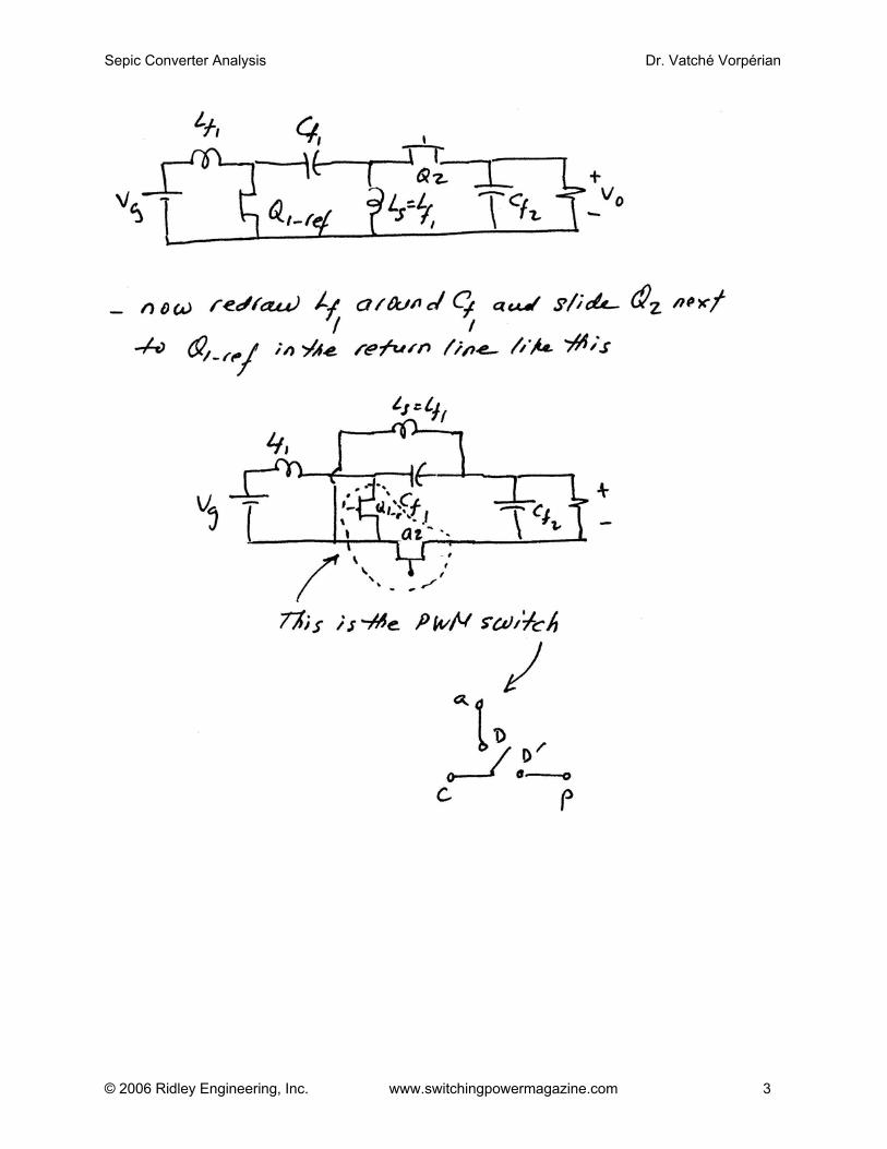
First, capacitor C1 is moved to the bottom branch of the converter. Then, inductor L2 is pulled over to the left, keeping its ends connected to the same nodes of the circuit. This reveals the PWM switch model of the converter, with its active, passive, and common ports, allowing us to use well-estab-lished analysis results for this converter.
For more background on the PWM switch model, the text book “Fast Analytical Techniques for Electrical and Electronic Circuits” [1] is highly recom-mended.
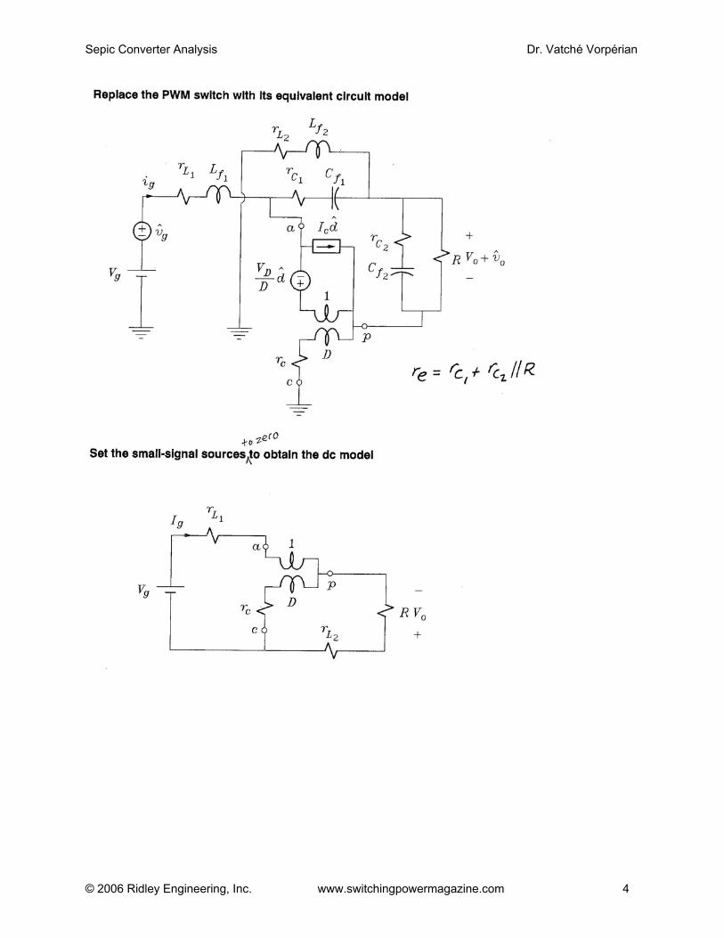
DC Analysis of the Sepic ConverterFig. 5 shows the equivalent circuit of
the Sepic converter with the DC portion of the PWM switch model in place. The DC model is just a 1:D transformer. We replace the inductors with short circuits, and the capacitors with open circuits for the DC analysis. You can, if you like, include any parasitic resistances in the model [2], but that’s beyond the scope of this article.
After the circuit is manipulated as shown in the figure, we can write the KVL equation around the outer loop of the converter:
Rearranging gives:
And the DC gain is given by:
Here we see the ability of the con-verter to step up or down, with a gain of 1 when D=0.5. Unlike the buck-boost and Cuk converters, the output is not inverted.
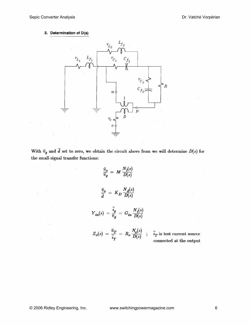
AC Analysis of the Sepic ConverterYou won’t find a complete analysis of
the Sepic converter anywhere in printed literature. What you will find are applica-tion notes with comments like, “the Sepic is not well-understood.” Despite the lack of documentation for the converter, engi-neers continue to use it when applicable.
Figure 5. For DC analysis, the small signal sources are set to zero, induc-tors become short circuits, and capaci-tors become open circuits. After the circuit is redrawn, it is a trivial matter to write KVL around the outer loop of the circuit to solve for the conversion gain of the converter.
Figure 6. The small-signal AC sources are included in the switch model, and we can either solve the analysis by hand, or use PSpice to plot desired transfer functions. The hand analysis is crucial for symbolic expressions and design equations.
Figure 4. In order to take advantage of Vorpérian’s PWM switch model, the circuit elements must first be rear-ranged. The function of the original topology is retained when the capaci-tor is moved, and the second inductor is redrawn.
Power Systems Design Europe November 200618
DESIGN TIPS
19www.powersystemsdesign.com
DESIGN TIPS
er? There are several possibilities. First, the dynamic and step load requirements on the system may be very benign, with no reason to design a loop with high bandwidth. This allows the loop gain to be reduced below 0 dB before the extreme phase delay of the second resonance.
Secondly, in many practical cases, the parasitic resistances of the circuit move the RHP zeros to the left half plane, greatly reducing the phase delay. This can also be done with the addition of damping networks to the power stage, a topic beyond the scope of this article.
Thirdly, some engineers do not build a proper Sepic. In some application notes, the two inductors are wound on a single toroidal core, which provides almost unity coupling between the two. In this case, the circuit no longer works as a proper Sepic. Don’t fall into this design trap - the circuit will be far from optimum.
Additional Reading[1] “Fast Analytical Techniques for
Electrical and Electronic Circuits”, Vatché Vorpérian, Cambridge University Press 2002. ISBN 0 521 62442 8.
[2] http://www.switchingpowermaga-zine.com. Click on Articles and Sepic Analysis Notes.
As you can see from these expres-sions, the “simplified” analysis is any-thing but simple. Including the para-sitic resistances greatly complicates the analysis, but may be necessary for worst-case analysis of the Sepic converter. The analysis of this converter involves the use of the powerful extra element theorem, and Vorpérian’s book on circuit analysis techniques. [1]
In addition to the inevitable fourth-order denominator of the Sepic, the most important features to note in the control transfer function are the terms in the numerator. The first term is a single right-half-plane (RHP) zero. Right-half-plane zeros are a result of converters where the response to an increased duty cycle is to initially decrease the output voltage.
When the power switch is turned on, the first inductor is disconnected from the load, and this directly gives rise to the first-order RHP zero. Notice that the expres-sion only depends on the input inductor, L1, the load resistor, R, and the duty cycle.
The complex RHP zeros arise from the fact that turning on the switch disconnects the second inductor from the load. These zeros will actually move with the values of parasitic resistors in the circuit, so careful analysis of your converter is needed to ensure stability under all conditions.
www.ridleyengineering.com
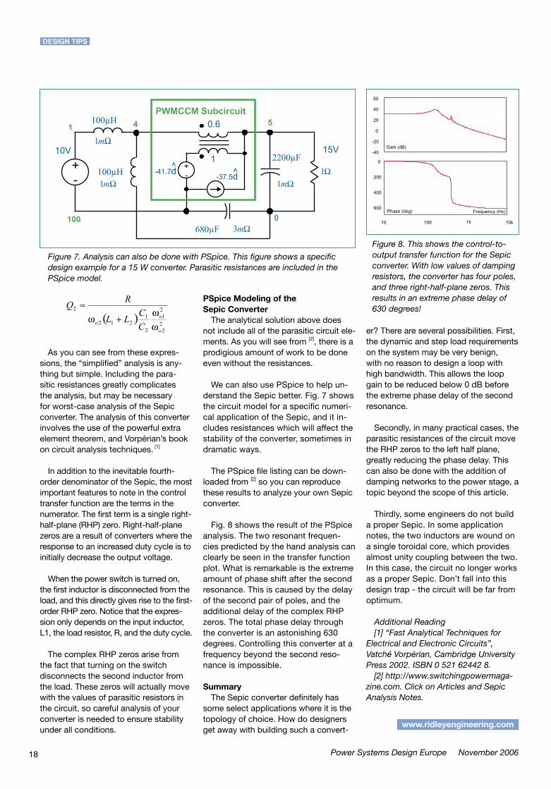
PSpice Modeling of the Sepic Converter
The analytical solution above does not include all of the parasitic circuit ele-ments. As you will see from [2], there is a prodigious amount of work to be done even without the resistances.
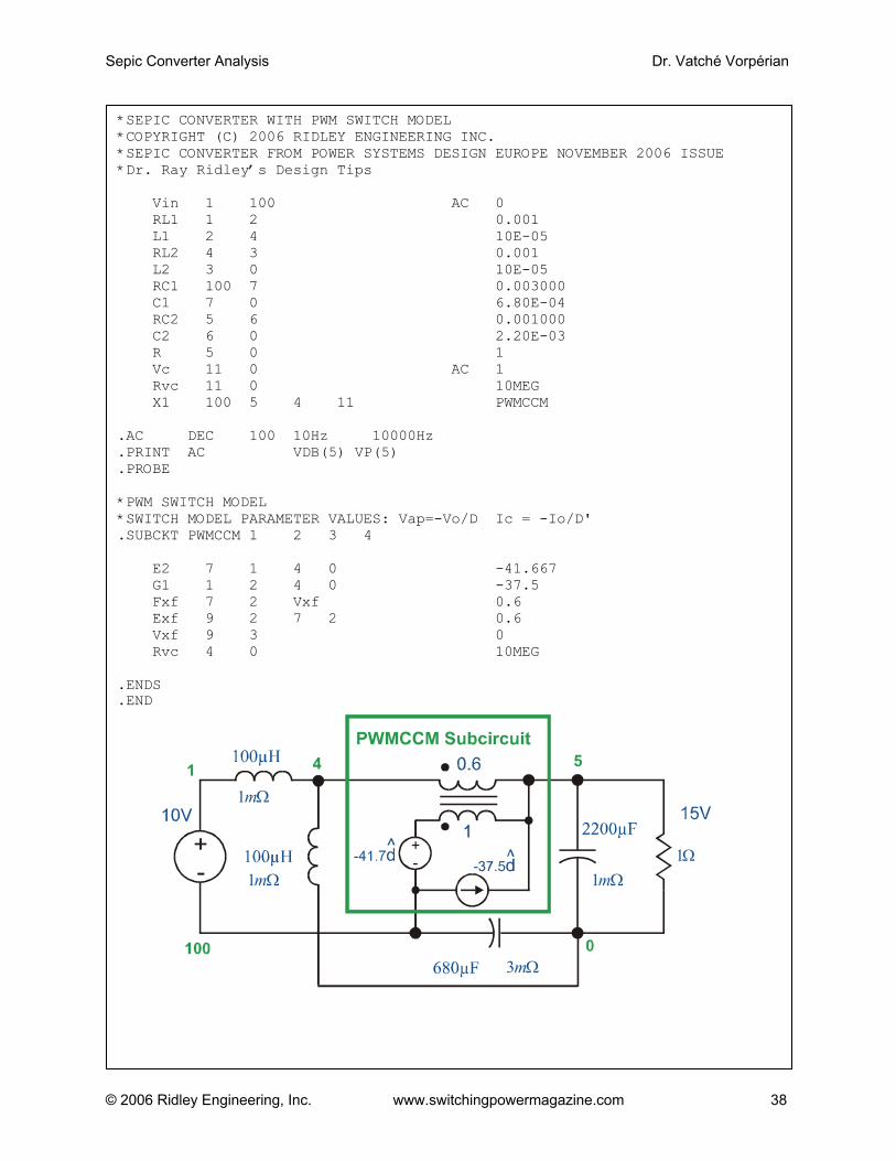
We can also use PSpice to help un-derstand the Sepic better. Fig. 7 shows the circuit model for a specific numeri-cal application of the Sepic, and it in-cludes resistances which will affect the stability of the converter, sometimes in dramatic ways.
The PSpice file listing can be down-loaded from [2] so you can reproduce these results to analyze your own Sepic converter.
Fig. 8 shows the result of the PSpice analysis. The two resonant frequen-cies predicted by the hand analysis can clearly be seen in the transfer function plot. What is remarkable is the extreme amount of phase shift after the second resonance. This is caused by the delay of the second pair of poles, and the additional delay of the complex RHP zeros. The total phase delay through the converter is an astonishing 630 degrees. Controlling this converter at a frequency beyond the second reso-nance is impossible.
SummaryThe Sepic converter definitely has
some select applications where it is the topology of choice. How do designers get away with building such a convert-
Figure 7. Analysis can also be done with PSpice. This figure shows a specific design example for a 15 W converter. Parasitic resistances are included in the PSpice model.
Figure 8. This shows the control-to-output transfer function for the Sepic converter. With low values of damping resistors, the converter has four poles, and three right-half-plane zeros. This results in an extreme phase delay of 630 degrees!

Serving North America and Asia . . .
Workshops
Products
Design Ideas
Consulting
Since 2000, Ridley Engineering has provided hands-on laboratoryworkshops for power supply design engineers. Now, RidleyEngineering Europe will continue this trend with a focus on Europe.
Since 1991, Ridley Engineering products have been available to designers worldwide.Products will now be available in Euros, shipped direct from within the EU:AP300 Frequency Response Analyzer & AccessoriesPOWER 4-55-66 Design Software - full version and customized AP300 version
For a wealth of design tips and design article archives, visit RidleyEngineering’s Design Resource Center at www.switchingpowermagazine.com
When designs become insurmountable in the lab, contact us for consulting services to assist in reaching production more efficiently.
Ridley Engineering, Inc. ~ 885 Woodstock Rd., Suite 430-382 ~ Roswell, GA 30075 ~ US ~ +1 770 640 9024 ~ Fax: +1 770 640 8714SARL Ridley Engineering Europe ~ Chemin de la Poterne ~ Monpazier 24540 ~ FR ~ +33 (0)5 53 27 87 20 ~ Fax: +33 (0)5 67 69 97 28Ridley Engineering UK Ltd. ~ 10 The Green ~ Bracknell, Berkshire RG12 7BG ~ UK ~ +44 (0)1344 482 493 ~ Fax: +44 (0)1344 204 632
Email: [email protected]
WWW.RIDLEYENGINEERING.COM

Sepic Converter Analysis Dr. Vatché Vorpérian
© 2006 Ridley Engineering, Inc. www.switchingpowermagazine.com 1
Analysis of the Sepic Converter
by
Dr. Vatché Vorpérian

Sepic Converter Analysis Dr. Vatché Vorpérian
© 2006 Ridley Engineering, Inc. www.switchingpowermagazine.com 2
Sepic Converter Analysis Dr. Vatché Vorpérian
© 2006 Ridley Engineering, Inc. www.switchingpowermagazine.com 3
Sepic Converter Analysis Dr. Vatché Vorpérian
© 2006 Ridley Engineering, Inc. www.switchingpowermagazine.com 4

Sepic Converter Analysis Dr. Vatché Vorpérian
© 2006 Ridley Engineering, Inc. www.switchingpowermagazine.com 5
Sepic Converter Analysis Dr. Vatché Vorpérian
© 2006 Ridley Engineering, Inc. www.switchingpowermagazine.com 6
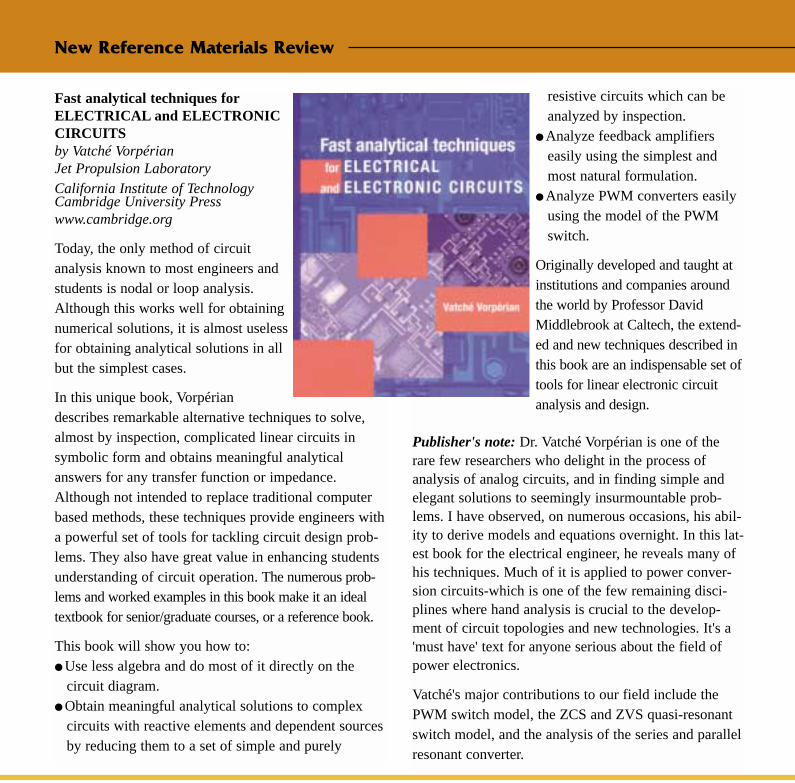
Fast analytical techniques forELECTRICAL and ELECTRONICCIRCUITSby Vatché VorpérianJet Propulsion LaboratoryCalifornia Institute of TechnologyCambridge University Presswww.cambridge.org
Today, the only method of circuitanalysis known to most engineers andstudents is nodal or loop analysis.Although this works well for obtainingnumerical solutions, it is almost uselessfor obtaining analytical solutions in allbut the simplest cases.
In this unique book, Vorpériandescribes remarkable alternative techniques to solve,almost by inspection, complicated linear circuits insymbolic form and obtains meaningful analyticalanswers for any transfer function or impedance.Although not intended to replace traditional computerbased methods, these techniques provide engineers witha powerful set of tools for tackling circuit design prob-lems. They also have great value in enhancing studentsunderstanding of circuit operation. The numerous prob-lems and worked examples in this book make it an idealtextbook for senior/graduate courses, or a reference book.
This book will show you how to: Use less algebra and do most of it directly on the
circuit diagram. Obtain meaningful analytical solutions to complex
circuits with reactive elements and dependent sources by reducing them to a set of simple and purely
resistive circuits which can be analyzed by inspection.
Analyze feedback amplifiers easily using the simplest and most natural formulation.
Analyze PWM converters easily using the model of the PWM switch.
Originally developed and taught atinstitutions and companies aroundthe world by Professor DavidMiddlebrook at Caltech, the extend-ed and new techniques described inthis book are an indispensable set oftools for linear electronic circuitanalysis and design.
Publisher's note: Dr. Vatché Vorpérian is one of therare few researchers who delight in the process ofanalysis of analog circuits, and in finding simple andelegant solutions to seemingly insurmountable prob-lems. I have observed, on numerous occasions, his abil-ity to derive models and equations overnight. In this lat-est book for the electrical engineer, he reveals many ofhis techniques. Much of it is applied to power conver-sion circuits-which is one of the few remaining disci-plines where hand analysis is crucial to the develop-ment of circuit topologies and new technologies. It's a'must have' text for anyone serious about the field ofpower electronics.
Vatché's major contributions to our field include thePWM switch model, the ZCS and ZVS quasi-resonantswitch model, and the analysis of the series and parallelresonant converter.
New Reference Materials Review
Winter 2002 issue, Designer Series’ Part VII. Wepublished a formula for temperature dependence of theR material. A minus sign was omitted in front of the lin-ear coefficient of the 5th order polynomial. The correctequation should be as follows:
where
(was +4.1658T ' in the original article.)
where T is in degrees C.
Thanks to Phil Cooke of Analog Devices for finding thiserror. We apologize for any inconvenience this mayhave caused.
Designer Series Part III, January 2001. we publishedan article on loop gain crossover frequency. The flybackconverter of Figure 1a had a typographical error - theoutput voltage of the converter should have been 12 V,not 24 V. If you run the calculation for the RHP zerowith 24 V output, you would have a frequency of 13.8
kHz instead of 20 kHz, and the maximumduty cycle would be 0.62.
Thanks to Fred Waechter of Phihong USA for findingthis error.
Corrections to Previous Articles in SPM
SUMMER~3 KPL 4/10/02 10:11 am Page 3
Ridley Engineering, Inc. ~ 885 Woodstock Rd., Suite 430-382 ~ Roswell, GA 30075 ~ US ~ +1 770 640 9024 ~ Fax: +1 770 640 8714SARL Ridley Engineering Europe ~ Chemin de la Poterne ~ Monpazier 24540 ~ FR ~ +33 (0)5 53 27 87 20 ~ Fax: +33 (0)5 67 69 97 28Ridley Engineering UK Ltd. ~ 10 The Green ~ Bracknell, Berkshire RG12 7BG ~ UK ~ +44 (0)1344 482 493 ~ Fax: +44 (0)1344 204 632
Email: [email protected]
WWW.RIDLEYENGINEERING.COM
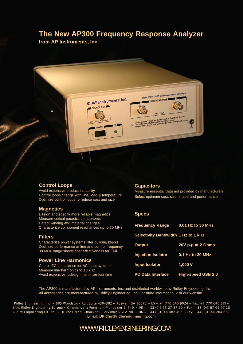
Control LoopsAvoid expensive product instabilityControl loops change with line, load & temperatureOptimize control loops to reduce cost and size
MagneticsDesign and specify more reliable magneticsMeasure critical parasitic componentsDetect winding and material changesCharacterize component resonances up to 30 MHz
FiltersCharacterize power systems filter building blocksOptimize performance at line and control frequency30 MHz range shows filter effectiveness for EMI
Power Line HarmonicsCheck IEC compliance for AC input systemsMeasure line harmonics to 10 kHzAvoid expensive redesign, minimize test time
CapacitorsMeasure essential data not provided by manufacturersSelect optimum cost, size, shape and performance
Specs
Frequency Range 0.01 Hz to 30 MHz
Selectivity Bandwidth 1 Hz to 1 kHz
Output 20V p-p at 2 Ohms
Injection Isolator 0.1 Hz to 30 MHz
Input Isolator 1,000 V
PC Data Interface High-speed USB 2.0
The New AP300 Frequency Response Analyzerfrom AP Instruments, Inc.
The AP300 is manufactured by AP Instruments, Inc. and distributed worldwide by Ridley Engineering, Inc.All accessories are manufactured by Ridley Engineering, Inc. For more information, visit our website.

Sepic Converter Analysis Dr. Vatché Vorpérian
© 2006 Ridley Engineering, Inc. www.switchingpowermagazine.com 7

Sepic Converter Analysis Dr. Vatché Vorpérian
© 2006 Ridley Engineering, Inc. www.switchingpowermagazine.com 8
Sepic Converter Analysis Dr. Vatché Vorpérian
© 2006 Ridley Engineering, Inc. www.switchingpowermagazine.com 9
Sepic Converter Analysis Dr. Vatché Vorpérian
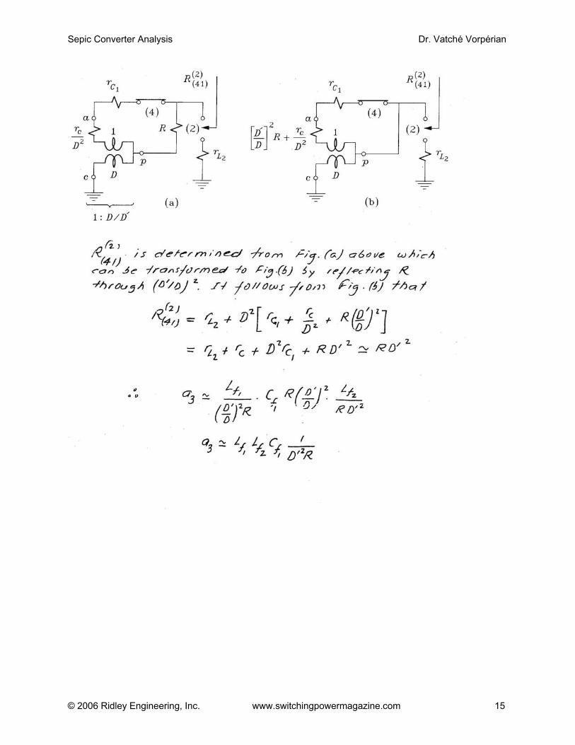
© 2006 Ridley Engineering, Inc. www.switchingpowermagazine.com 10
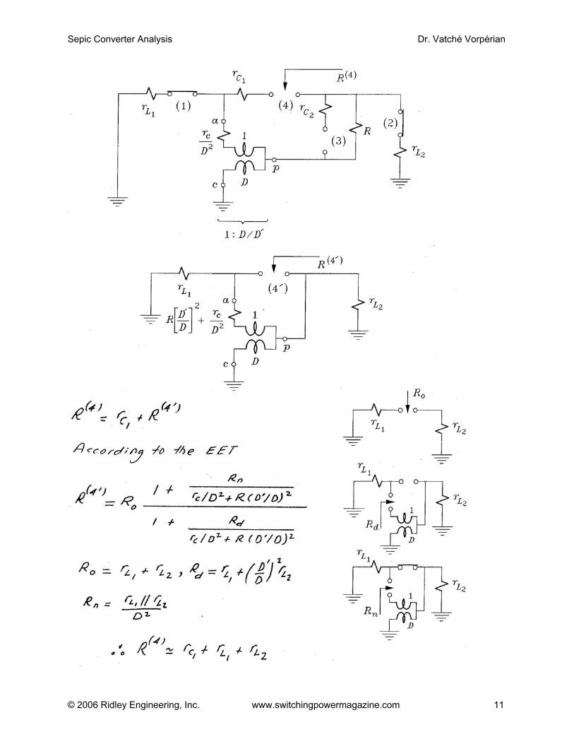
Sepic Converter Analysis Dr. Vatché Vorpérian
© 2006 Ridley Engineering, Inc. www.switchingpowermagazine.com 11
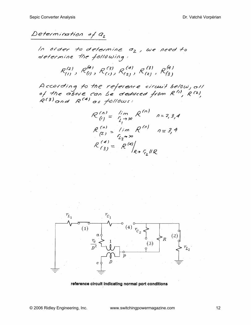
Sepic Converter Analysis Dr. Vatché Vorpérian
© 2006 Ridley Engineering, Inc. www.switchingpowermagazine.com 12

Ridley Engineering, Inc. ~ 885 Woodstock Rd., Suite 430-382 ~ Roswell, GA 30075 ~ US ~ +1 770 640 9024 ~ Fax: +1 770 640 8714SARL Ridley Engineering Europe ~ Chemin de la Poterne ~ Monpazier 24540 ~ FR ~ +33 (0)5 53 27 87 20 ~ Fax: +33 (0)5 67 69 97 28Ridley Engineering UK Ltd. ~ 10 The Green ~ Bracknell, Berkshire RG12 7BG ~ UK ~ +44 (0)1344 482 493 ~ Fax: +44 (0)1344 204 632
Email: [email protected]
WWW.RIDLEYENGINEERING.COM
Now in its 18th year of development, POWER 4-5-6Plus is the most powerful design, analysis, and simulation software available for power supplydevelopment. The latest version includes topologyselection, detailed magnetics design, capacitorselection, and feedback design in addition to voltage-mode or current-mode control.
Unlike other simulation packages, POWER 4-5-6can run simulations of converter designs within minutes. It allows you to trade off and assess differ-ent design options faster than you thought possible.
While you are busy working on power stage component analysis, POWER 4-5-6 will constantlyoptimize a control loop for your choices. This allowsyou to immediately see the effect of your changeson dynamic response, and ensures that you reach
steady-state quickly to properly assess the effect ofcircuit changes on component stresses. No otherprogram offers this capability.
The magnetics designer in POWER 4-5-6 providesa library of cores and wire types. Our advancedproximity loss analysis feature shows the effect ofac winding losses, to ensure that you choose thebest combination of wire sizes and winding layersfor minimal dissipation. Entering new cores into thelibrary is simple and fast.
And now, a special version of the software is available for AP300 Frequency Response Analyzerusers that predicts the response of your power supply and compares it with data collected from theAP300. They communicate with each other to showmeasurements overlaid on theoretical curves.
The World’s Most Comprehensive Design Software from Ridley Engineering, Inc.

Sepic Converter Analysis Dr. Vatché Vorpérian
© 2006 Ridley Engineering, Inc. www.switchingpowermagazine.com 13

Sepic Converter Analysis Dr. Vatché Vorpérian
© 2006 Ridley Engineering, Inc. www.switchingpowermagazine.com 14
Sepic Converter Analysis Dr. Vatché Vorpérian
© 2006 Ridley Engineering, Inc. www.switchingpowermagazine.com 15

Sepic Converter Analysis Dr. Vatché Vorpérian
© 2006 Ridley Engineering, Inc. www.switchingpowermagazine.com 16

Sepic Converter Analysis Dr. Vatché Vorpérian
© 2006 Ridley Engineering, Inc. www.switchingpowermagazine.com 17

Sepic Converter Analysis Dr. Vatché Vorpérian
© 2006 Ridley Engineering, Inc. www.switchingpowermagazine.com 18
SARL Ridley Engineering Europe ~ Chemin de la Poterne ~ Monpazier 24540 ~ FR ~ +33 (0)5 53 27 87 20 ~ Fax: +33 (0)5 67 69 97 28Ridley Engineering UK Ltd. ~ 10 The Green ~ Bracknell, Berkshire RG12 7BG ~ UK ~ +44 (0)1344 482 493 ~ Fax: +44 (0)1344 204 632Ridley Engineering, Inc. ~ 885 Woodstock Rd., Suite 430-382 ~ Roswell, GA 30075 ~ US ~ +1 770 640 9024 ~ Fax: +1 770 640 8714
Email: [email protected]
WWW.RIDLEYENGINEERING.COM
The AP300 Analyzer and POWER 4-5-6 Software aredesigned specifically for the power electronics engineer.Now, they communicate with each other to show measurements overlaid on theoretical curves.
The analyzer has advanced features including a highpower output, variable source vs. frequency curve, andhigh noise immunity from 0.01 Hz to 30 MHz.
POWER 4-5-6 greatly accelerates your design processin topology choices, magnetics, and control. A specialversion of the software predicts the response of yourpower supply and compares it with data collected fromthe AP300.
Each product is the best available in the industry.Together, they will take your design and testing skills tothe next level.
Sepic Converter Analysis Dr. Vatché Vorpérian
© 2006 Ridley Engineering, Inc. www.switchingpowermagazine.com 19
Sepic Converter Analysis Dr. Vatché Vorpérian
© 2006 Ridley Engineering, Inc. www.switchingpowermagazine.com 20
Sepic Converter Analysis Dr. Vatché Vorpérian
© 2006 Ridley Engineering, Inc. www.switchingpowermagazine.com 21

Sepic Converter Analysis Dr. Vatché Vorpérian
© 2006 Ridley Engineering, Inc. www.switchingpowermagazine.com 22

Sepic Converter Analysis Dr. Vatché Vorpérian
© 2006 Ridley Engineering, Inc. www.switchingpowermagazine.com 23

Sepic Converter Analysis Dr. Vatché Vorpérian
© 2006 Ridley Engineering, Inc. www.switchingpowermagazine.com 24

Gain a lifetimeof design experience
. . . in four days
In this four-day intensive workshop, the first half of eachday focuses on theory, design ideas, control schemes,and magnetics applications, all taught by Dr. RayRidley. Each afternoon is spent in our state-of-the-artlaboratory exploring and applying concepts, windingcustom magnetics, building and testing circuits, andoptimizing designs. Our practical, hands-on approachteaches engineers with all levels of experience how tobe more efficient designers. Learn how to use POWER4-5-6, the world’s most comprehensive design software.
Dr. Ridley combines the teaching of theoretical andpractical concepts, and hands-on experience withdesign software and laboratory instruments. It's an educational opportunity you can't afford to miss.
Tuition includes training, lab notes, POWER 4-5-6 software, and lunch. Only 24 seats are available ateach workshop. Visit our website for additional information and reservations.
WWW.RIDLEYENGINEERING.COM
FR: SARL Ridley Engineering Europe ~ Chemin de la Poterne ~ Monpazier 24540+33 (0)5 53 27 87 20 ~ Fax: +33 (0)5 67 69 97 28
UK: Ridley Engineering UK Ltd. ~ 10 The Green ~ Bracknell, Berkshire RG12 7BG ~ UK +44 (0)1344 482 493 ~ Fax: +44 (0)1344 204 632
US: Ridley Engineering, Inc. ~ 885 Woodstock Rd., Suite 430-382 ~ Roswell, GA 30075 +1 770 640 9024 ~ Fax: +1 770 640 8714
Email: [email protected]

Sepic Converter Analysis Dr. Vatché Vorpérian
© 2006 Ridley Engineering, Inc. www.switchingpowermagazine.com 25
Sepic Converter Analysis Dr. Vatché Vorpérian
© 2006 Ridley Engineering, Inc. www.switchingpowermagazine.com 26

Sepic Converter Analysis Dr. Vatché Vorpérian
© 2006 Ridley Engineering, Inc. www.switchingpowermagazine.com 27

Sepic Converter Analysis Dr. Vatché Vorpérian
© 2006 Ridley Engineering, Inc. www.switchingpowermagazine.com 28
Sepic Converter Analysis Dr. Vatché Vorpérian
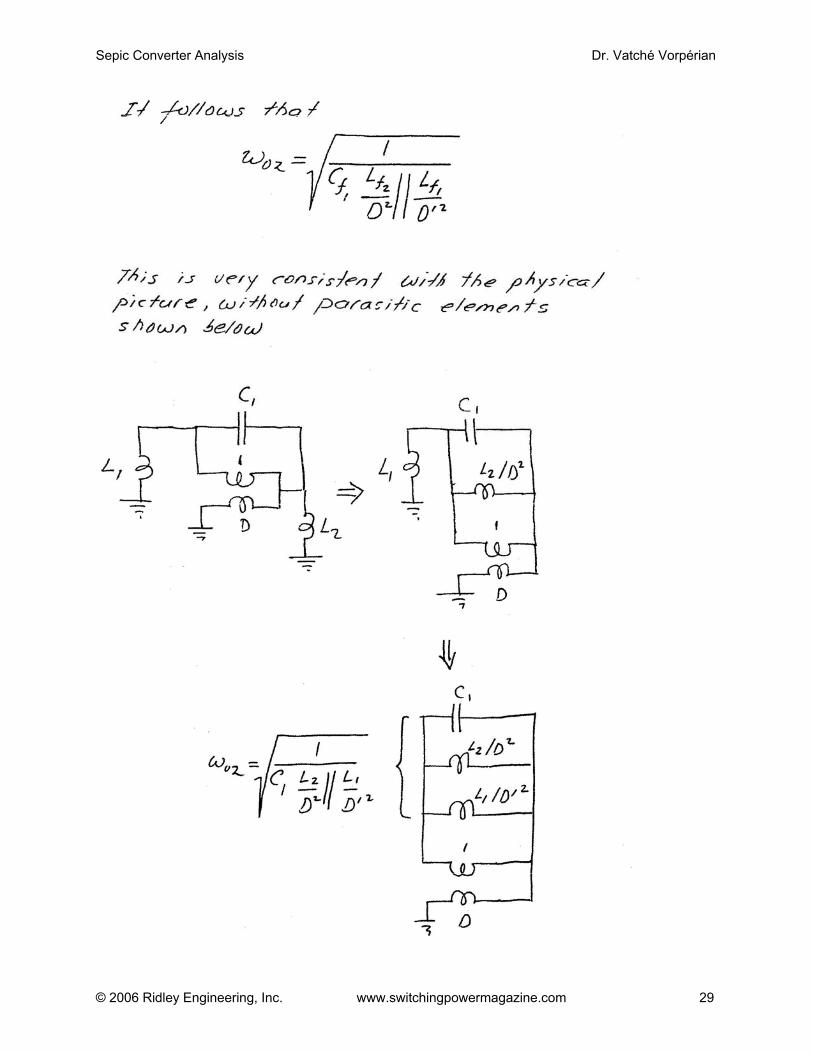
© 2006 Ridley Engineering, Inc. www.switchingpowermagazine.com 29

Sepic Converter Analysis Dr. Vatché Vorpérian
© 2006 Ridley Engineering, Inc. www.switchingpowermagazine.com 30

Sepic Converter Analysis Dr. Vatché Vorpérian
© 2006 Ridley Engineering, Inc. www.switchingpowermagazine.com 31
Sepic Converter Analysis Dr. Vatché Vorpérian
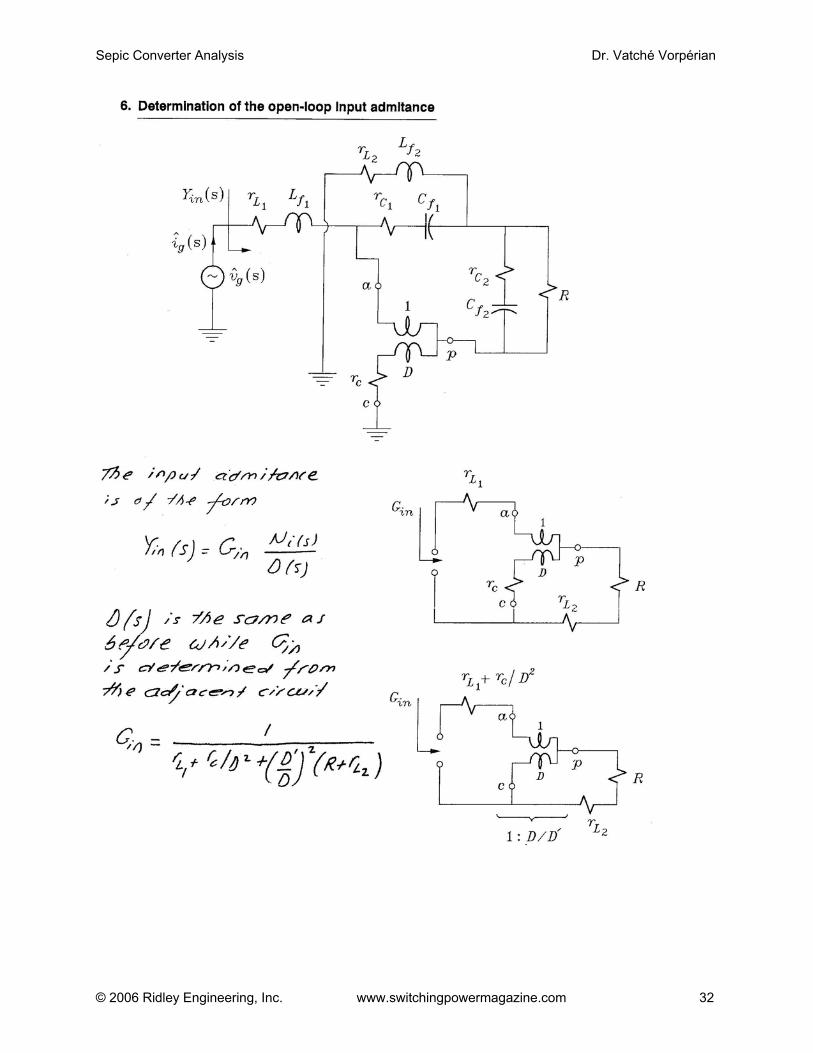
© 2006 Ridley Engineering, Inc. www.switchingpowermagazine.com 32

Sepic Converter Analysis Dr. Vatché Vorpérian
© 2006 Ridley Engineering, Inc. www.switchingpowermagazine.com 33

Sepic Converter Analysis Dr. Vatché Vorpérian
© 2006 Ridley Engineering, Inc. www.switchingpowermagazine.com 34

Sepic Converter Analysis Dr. Vatché Vorpérian
© 2006 Ridley Engineering, Inc. www.switchingpowermagazine.com 35

Sepic Converter Analysis Dr. Vatché Vorpérian
© 2006 Ridley Engineering, Inc. www.switchingpowermagazine.com 36
Sepic Converter Analysis Dr. Vatché Vorpérian
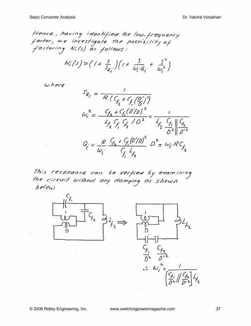
© 2006 Ridley Engineering, Inc. www.switchingpowermagazine.com 37
Sepic Converter Analysis Dr. Vatché Vorpérian
© 2006 Ridley Engineering, Inc. www.switchingpowermagazine.com 38
*SEPIC CONVERTER WITH PWM SWITCH MODEL *COPYRIGHT (C) 2006 RIDLEY ENGINEERING INC. *SEPIC CONVERTER FROM POWER SYSTEMS DESIGN EUROPE NOVEMBER 2006 ISSUE *Dr. Ray Ridley’s Design Tips Vin 1 100 AC 0 RL1 1 2 0.001 L1 2 4 10E-05 RL2 4 3 0.001 L2 3 0 10E-05 RC1 100 7 0.003000 C1 7 0 6.80E-04 RC2 5 6 0.001000 C2 6 0 2.20E-03 R 5 0 1 Vc 11 0 AC 1 Rvc 11 0 10MEG X1 100 5 4 11 PWMCCM .AC DEC 100 10Hz 10000Hz .PRINT AC VDB(5) VP(5) .PROBE *PWM SWITCH MODEL *SWITCH MODEL PARAMETER VALUES: Vap=-Vo/D Ic = -Io/D' .SUBCKT PWMCCM 1 2 3 4 E2 7 1 4 0 -41.667 G1 1 2 4 0 -37.5 Fxf 7 2 Vxf 0.6 Exf 9 2 7 2 0.6 Vxf 9 3 0 Rvc 4 0 10MEG .ENDS .END
+-
+-
Ωm3
Ωm1
Ωm1 Ω1
Ωm1

Serving the European Community
Announcing a new location . . .
Workshops
Products
Design Ideas
Consulting
Since 2000, Ridley Engineering has provided hands-on laboratoryworkshops for power supply design engineers. Now, RidleyEngineering Europe will continue this trend with a focus on Europe.
Since 1991, Ridley Engineering products have been available to designers worldwide.Products will now be available in Euros, shipped direct from within the EU:AP300 Frequency Response Analyzer & AccessoriesPOWER 4-55-66 Design Software - full version and customized AP300 version
For a wealth of design tips and design article archives, visit RidleyEngineering’s Design Resource Center at www.switchingpowermagazine.com
When designs become insurmountable in the lab, contact us for consulting services to assist in reaching production more efficiently.
SARL Ridley Engineering Europe ~ Chemin de la Poterne ~ Monpazier 24540 ~ France ~ +33 (0)5 53 27 87 20Ridley Engineering UK Ltd. ~ 10 The Green ~ Bracknell, Berkshire RG12 7BG ~ UK ~ +44 (0)1344 482 493
Ridley Engineering, Inc. ~ 885 Woodstock Rd., Suite 430-382 ~ Roswell, GA 30075 ~ US ~ +1 770 640 9024Email: [email protected] ~ Fax: +1 770 640 8714
WWW.RIDLEYENGINEERING.COM