september 1968 - core
TRANSCRIPT

1
SYNTHESIS OF BRANCH-GUIDE DIRECTIONAL
COUPLERS AND FILTER PROTOTYPES
by
L. F. LIPID
A thesis presented for the degree of Doctor of
Philosophy at the University of Leeds
September 1968

2
Acknowledgments
The author wishes to express his gratitude to Dr. R.
Levy for his continual and experienced guidance, to Dr. J.
Scanlan for his much valued advice and to Professor G. W.
Carter for the use of the facilities of the'Electrical
Engineering Department.
The author is also indebted to the Ministry of Technology
which supported this research.

3
List of Contents Page No
Acknowledgments. 2
Chapter 1. Introduction. 6
1.1 Object of the thesis. 6
1,2 The philosophy of circuit' theory. 6
1.3 Lumped and distributed network theory. 7
1.4 The synthesis of equally terminated, 9
low-pass filters of even order.
1.5 Branch-guide directional couplers. 10
Chapter 2. Lumped Element Network Synthesis. 13
2.1 Properties of the driving-point impedance. 13
2.2 The voltage reflection coefficient. 19
2.3 Two-terminal-pair network parameters. 21
2.4 The Darlington insertion-loss synthesis technique. 28
2.4.1 Theory 28
2,4.2 An example of the Darlington method:
the Butterworth specification. 32
2.5 The scattering matrix. 37
2.6 Determination of phase from a magnitude
specification. 44
References in chapter 2.48
Chapter 3. Transmission Line Network Synthesis. 49
3.1 Introduction. 49
3.2 The tangent transformation. 51
4
3.3 Driving-point Impedances and Richards'
theorem.
3.4 Cascaded transmission line networks.
References in chapter 3.
Chapter 4. Synthesis of Low-Pass Lumped and Distributed
Filters.
4.1 Conventional Chebyshev design.
4.2 Modified design theory.
4.3 Synthesis of even N, equally terminated, low-
pass filters.
4.3.1 Lumped element filters.
4.3.2 Distributed element filtere.
4.4 Concluding remarks.
4.5 Proof that the Ln polynomials are optimal.
References In chapter 4.
Chapter 5. Branch-Guide Directional Couplers.
5.1 General directional coupler theory.
5.1.1 The scattering matrix.
5.1.2 The symmetric directional coupler.
5.1.3 The symmetric hybrid junction.
5.1.4 Directional coupler even and odd
mode analysis.
5.2 Development of symmetric branch-guide
directional couplers.
Page No.
53 62
66
67 67
73
78
78 85
9o 93
96
98
98
98
102
105
108

5.2.1 Basic description.
5.2.2 Analysis of the branch-guide coupler.
5.2.3 Early developments.
5.2.4 Patterson's theory.
5.2.5 Young's theory.
5.3 New design theory.
5.3.1 General considerations.
5.3.2 Coupler analysis.
5.3.3 The approximation problem.
5.3.4 The Butterworth specification.
5.3.5 The Chebyshev specification.
5.3.6 The synthesis procedure.
5.3.7 K vs. coupling.
5.3.8 Example of the synthesis procedure.
5.4 Discussion of computed results.
5.4.1 The symmetrical case.
5.4.2 The asymmetrical case.
5.5 Experimental results.
5.6 Concluding remarks.
References in: chapter 5.
Chapter'6. Conclusions and Possible Developments.
9

6
Chapter 1.
Introduction.
1.1 Object of. the. Thesis.
The object of this thesis is the solution of the following
problems using the theories of lumped and distributed network
synthesis: (1) Synthesis of equally terminated, lumped and. distributed
filters containing an even number of elements.
(2) Synthesis of. symmetrical and asymmetrical branch-.
guide directional couplers.
1.2 The Philosophy of Circuit Theory.
In the past twenty years, network synthesis has been well
developed for networks containing lumped elements. More recently,
network synthesis techniques have been devised for networks con-
taining distributed elements.
Network synthesis is' in itself a basic discipline which
may be applied to a large variety. of physical problems. It
consists fundamentally: of three aspects, e. g.
(1) Realizability criteria,
(2) Approximation,
(3) Synthesis.
The existence of realizability, criteria means that network
theory has been brought to a stage of development well ahead
of many other subjects, since it enables, one to tell, in ad-

7
vance whether a problem possesses a solution physically obtain-
able using elements of specified form. It is extremely valuable
to know in advance whether a problem or class of problems does
or does not possess a solution because of fundamental limits-
tions.
Once it is established that a solution to a problem exists,
then it is usually possible to approximate to the ideal as
closely as one pleases. This is the branch of circuit theory
classified above as part (2). Once a suitable approximating
function has been determined:,, * then, provided it satisfies the
criteria of physical realizability, the third'part of circuit
theory consists'in synthesizing the approximation function
exactly. A large variety of synthesis techniques have been
developed for this purpose; in general each different tech-
nique leads to a different network structure.
1.3 Lumped and Distributed Network Theory.
In Chapter 2 the fundamentals of lumped element network
synthesis which are necessary in the later chapters are dis-
cussed. The development. is restricted to two-port ladder
structures (which contain reciprocal, linear, passive,, and
time invariant elements), as the ladder structure is the
only structure used for synthesis purposes in this thesis.
The properties of a positive real driving-point impe-
dance and the associated bounded real voltage reflection

8
coefficient are described in detail. Then, through the de-
velopment of the network transfer matrix, the concept of
network insertion lose is introduced.
This leads naturally to the introduction of Darlington's
insertion-lose synthesis technique,. for which both the theory
end a numerical example are presented.
An extension of the insertion loss definition of a two-
port to an n-port is given next, through the use of the scatter-
ing matrix. Its properties of symmetry, existence, and the
unitary condition (for a lossless network) are derived, these
properties being useful when the scattering matrix of a direc-
tional coupler is examined.
The last section in chapter 2 discusses a phase-magnitude
relationship' of an analytic function, which is also used to
advantage in the directional coupler work.
In chapter 3 it is shown how lumped element network theory
is extended by Richards' transformation to apply to distribu-
ted networks. An additional two port circuit element, a length
of transmission line (unit element) is introduced here which
has no counterpart in lumped circuit theory.
The properties of a cascade of unit elements terminated
at either end by resistors (a distributed filter) are discussed
in the last section of this chapter.
9
1_4 The Synthesis of Equally Terminated, Low-Pass Filters
of Even Order.
In the conventional synthesis of doubly terminated
lumped and distributed filters, Chebyshev polynomials of the
first kind are used when an equiripple insertion loss specifica-
tion is desired. A shortcoming of using Chebysher polynomials
of even degree in this insertion loss specification is that
they yield filters having an unequal resistance ratio in the
case of low-pass filters.
A modified low-pass equiripple polynomial of even degree
has been found independently by the author (and by others) with
the desirable property that its value at the origin may be
shifted to any level below its passband ripple level, including
zero (the condition necessary for equally terminated designs).
The properties of this polynomial are examined in chapter 4,
and then it is used to synthesize lumped and distributed
equally terminated filters. The standard Darlington synthesis
technique is employed for this purpose.
A computer program was written to perform this synthesis. %
It was found that for the higher degree filters a conformal
transformation was necessary in the synthesis to preserve
numerical accuracy. Use of this mapping function for the dis-
tributed case represents original work in that the mapping
has thus far been developed and used only for lumped element

10
synthesis. Tables of element values are presented for a wide
range of input specifications. The tables were used in the de-
sign of a coaxial low-pass filter. The measured VSWR frequency
performance was found to agree quite closely with the theoretical
performance. In the final section of chapter 4, a proof showing
that the modified polynomial is optimal (under suitable restric-
tions) is given.
1.5 Branch-Guide Directional Couplers.
At the beginning of chapter 5 the definition of a direc-
tional coupler is stated. Then, through the use of scattering
matrix properties which were developed in chapter 2, proper-
ties of perfect and nearly perfect symmetric directional couplers
are discussed. Also a description is given of the decomposition
of a four port directional coupler into two related two-port
networks, through the use of an even and odd mode analysis.
The discussion then becomes more specialized by consider-
Ing only one type of directional coupler, the branch-guide
directional coupler. A brief history of the development of
symmetric branch-guide directional couplers is presented, and
the shortcomings of these design theories are examined in
detail.
It is at this point that the original work contained in
this thesis on branch-guide directional couplers is introduced.

11
J
A new design theory is presented, which allows for symmetric
as well as asymmetric couplers.
First the general form of the approximation function is
found. Then two specification functions, the Butterworth and
Chebyshev approximations, are presented, both of which possess
the required form.
A , description of the complete synthesis process (which
uses the Darlington synthesis technique) is given next, and
illustrated by a numerical example.
Tables for both Butterworth and Chebyshev symmetrical
and asymmetrical couplers are presented which should cover
most cases of practical interest.
The asymmetric directional coupler requires an unequal
output to input resistance ratio. In this respect. it also may
be regarded as an impedance transformer. It represents a new
structure which has not yet been described in the literature.
It is found that for similar input specifications the asym-
metric coupler has a larger bandwidth than the symmetric
coupler. Several designs resulting from the new synthesis tech-
nique for both Butterworth and Chebyshev symmetrical couplers
have been constructed both in X-band waveguide and in strip-
line. The experimental and theoretical results are described,
and it is found that there is quite close agreement between
the two.

12
It is found that the new synthesis technique for sym-
metrical couplers gives superior results compared with previous
approximate methods both for the Butterworth and Chebyshev cases.
The design of couplers having a bandwidth greater than one
octave appears to be feasible.

13
Chapter 2.
Lumped element Network Synthesis.
2.1 Properties of the Driving-Point Impedance.
Consider a network composed of elements which are lumped,
linear, bilateral, time invariant, and passive. The types of
elements which fit this description are resistors, capacitors,
and coils (having both self and mutual inductance). Kirchoff's
equilibrium equations for the m t1 node network, on a nodal basis,
may be written as
Yll v1 + y12 Y2 + ... i-ylm Vm
(2.1) Y21 v1 -f- Y22 Y2 4.... t Y2m vm = I2
1ml Vl t ym2 V2 +- .... }-Ymm Vm _ Im 9
where yil is the admittance between node i and the common
(datum) node, with all other nodes joined to datum, yik is the
admittance between nodes i and k, and Ik is the input (source)
current to node k. To simplify matters, all of the current
sources are assumed to have the same sinusoidal time variation
Ik IkeMore complicated waveforms may be expressed as
a Fourier series and the principle of Superposition- is then
applied to obtain the total result. From the postulates of
linearity and time invariance it is seen that the Vk must also
have this eJWt time variation so that it cancels out on both
sides of the equation.

34
The nodes for this network are chosen so that the admit-
tance yik has the form
yik _ jk+JwCik +- 1 (2.2) J wLik
Mutual inductances are avoided by replacing each coil pair
containing mutual inductance by a three-coil potentially
equivalent Pi or T network.
Now it is convenient to introduce the generalized complex
variable s defined by
is - Cr +Jw, (2.3)
where o- and w are real variables. This complex variable a
is the same as the Laplace transform variable' a, eo
i. e. L (f(t)) = F(s) _ Sf(t)e-8
at, (2.4) a
where F(s) is the complex frequency transform of the time wave-
form f(t). This f(t) is assumed to have zero value for t4 to.
Substituting (2.3) into (2.2), yik may be written as
yik Gig -F' sCik .-1 (2.5)
sLik
This apparently simple step is of great importance, since now
yik is a real function of the complex variable a. Furthermore,
it'may be shown that yik and indeed any rational function R(s)
is an analytic function of a (satisfies the Cauchy-Riemann
equations) over the entire s-plane, excepting the points. at
which R(s) becomes infinite in value(commonly referred to as the
poles of R(s)). Analytic function theory has been developed
into a powerful mathematical tool, and certain results from this

35
theory will be used in the following work.
One immediate application of analytic function theory
results from the uniqueness theorem, which states that two analytic
functions which have identical values on an arbitrary finite line
segment in the complex plane must have identical values over
their entire region of analyticity (for rational functions,
over the finite complex plane, excepting the pole points, of
course) and thus be identical. This theorem leads to the principle
of analytic continuation. In Eq. (2.2) yik is defined on the ima-
ginary axis of the a-plane. By using the above theorem, it is
seen that yik may now be defined uniquely over the entire finite
d-plane (Eq. (2.5)) by a knowledge of its values on the imaginary
axis, ie. yik(Jw) has been analytically continued into the e-
plane.
In Eq. (2.1) all of the yik are now assumed to be functions
of s. This equation may be solved for the voltages by using
standard determinant methods to yield
V 11 11 1 21 I2 ...
dml lm ,
v2=. LA
12 I1 ý22 12 ... Lm2 Im , (2.6)
A. Li L.
------------- vm= Aim I1 1ý2m 12 ..
dmm Im I 0
where t, is the determinant of the y matrix in Eq. (2.1) and d
jg is the corresponding cofactor of this determinant.

16
Now the open-circuit driving-point impedance for the first
part of this network may be defined as
Q11-- V1
I1 12 7- 13 = ..: = Im =0 (2.7)
From Eq. (2.6) it is seen that
t11 = all
(2.8)
where A
11 and A
are rational functions of s, and each consists
of sums of products of the basic admittances given by Eq. (2.5).
Thus Oll will have the form
eil ._.
ao gn + al an-1 + ... + an. N8), i2.9, )
bo sä ". - bl ad-1 + ... + bn ID(a)
in which all of the ai and bi are real numbers.
The fundamental theorem of algebra states that a polynomial
of degree n will have n (generally complex) roots. Since the ai
and bi are real, any complex roots of N(s) or D(e) in Eq. (2.9)
must occur in conjugate paira.
Assuming that the network is initially quiescent, a unit
impulse of current is now suddenly applied at the first port
at t =o. The Laplace transformof this current is given by
Eq. (2.4) as
I1(s) = Ste_5t
. 1. (2.10)

17
Substituting this current into Eq. (2.7),
all(e) -. v1(s), (2.11)
and hence,.
V1(t) = L-1 (iie))
(2.12)
Expanding Eq. (2.9) into partial fraction form gives
Zll(s) k=1
ab =+ " -",:, Bk t. e-ak k=1 e , 7Z
Ck . (2.13)
k=2 s-e,
By the use of standard inverse Laplace transforms, Y1(t) is ob-
tained from Eqs. (2.12) and (2.13) as
Vl(t) _ Akeskt Bktk-1 + Pab,. b;
ý CJ k k=1 k=1 (k-1) J k=2 tk-leSjt.
(k-1):
(2.14)
Since the network is assumed not to contain any energy
sources, V1(t) can only have a damped exponential or damped oscil-
latory exponential response, or, in extreme cases, have a steady
d. c. or oscillatory response. Term by term inspection of Eq. (2.14)
yields the conditions necessary for this sort of response:
1) If the pole is simple, its real part cannot be greater
than zero.
2) A pole at the origin must be a simple pole.
3) If the pole is of multiple order, its real part is less
than zero.
18
An analogous analysis may now be done for the short-circuit
driving-Point admittance Y11(s), whose poles are the zeros of
Z11(s), and the same set of conditions are found to hold.
In conclusion, a necessary condition for S to be a zero
or pole of z11(s) is that its real part is negative, or may be
zero if the zero or pole is simple. In terms of the complex
s_plane, the poles and zeros- of 211(s) are in the left half
s-plane, and, if on the imaginary axis,. must be simple. As it
turns out, this is a necessary but not sufficient requirement
if ell(s) is to represent the open-circuit driving-point im-
pedance of a passive network.
Intuitively, it is also known that
Re (1l(s)
s=Jw 0 for -oo6wcoo (2.15)
where Re stands for "the real part of".
If the real part of 211 were negative at some frequency,
it wouldimply that energy could be extracted from the passive
network at that frequency, which is impossible (assuming the
network is initially quiescent).
Now Z11 does not possess any poles in the right half s-
plane, and thus is analytic (satisfies the Cauchy-Riemann. equations)
there. An important result from analytic function theory states
that if a function is analytic over a region R of the complex
plane and does not have a zero in R, its real part attains both
its minimum and maximum value over R on the boundary of R. By
using this result and Eq. (2.15), it follows that
Re (ä11(a) Z0, Re (e)20
. (2.16)
; 19
A function which satisfies this condition is known as a
positive function. It has also been shown that W11(s) possesses
real coefficients, such that when s is real Zll(s) is also purely
real. This type of function is known as a real function. A
function that possesses both of these properties is known as
a positive real (p. r. ) function. Thus it is necessary for
z11(s) to be a p. r. function. It can also be shown that the
p. r. condition is sufficient for Z11(s) to represent the open-
circuit driving-point impedance for a passive network. This
fact is shown through the development of a general network
realization technique (1), which has as its starting point a
p. r. 2Il(e).
2.2 The Voltage Reflection Coefficient.
The input impedance Z11, however, is not a convenient.
function to specify in the work that follows. A useful function
which is closely related to zll, the voltage reflection coef-
ficient r, is therefore now examined. For the network in
Fig-2-1, where all impedances have been normalized so that
Zs=l-R, r' is defined by
Za- Za -Es-; j (2.17)
z(a) t äa 8(a) i- 1
where a(s)= Z11(s). Eq. (2.17), in analytic function theory
terms, may be viewed as a conformal mapping of the Z-plane into
thef -plane. It is easily shown that the right half of the Z-
plane becomes the region inside a circle of unit radius centered
at the origin in the r-plane, and that the imaginary axis of the
z-plane transforms into the circle of unit radius in the r -plane.

zs . 1. n Network Network
z, r
Fig. 2.1. Definition of the voltage reflection coefficient ('.
20
Hence,
I r()I s1 for Re {Z(s)} >_ 0. (2.18)
In the previous section it was seen that Z(s) must be a
positive real function, and so, from Egs. (2.16) and (2.18),
f r(a)I! 1 for Q'>_ 0. (2.19)
Thus j (s)I is bounded (by unity) for values of s whose real
part is equal to or greater than zero. It is easily shown from
Eq. (2.17) that r (s) is real when a is real (since Z(s) is real
then). A function which possesses both of these properties is
called a bounded real (b. r. ) function. Conversely, if the bound
in Eq. (2.18) holds for an arbitrary b. r. r (s), then the Z(s)
calculated from this r (s) is necessarily p. r., and may be
developed into a realizable passive network.
Another important result from analytic function theory
is the maximum modulus theorem, which states that if a function
of a complex variable is analytic over a region R, its absolute
value (modulus) at any point-of R is less than or equal to the
maximum modulus over the boundary of R.
Now, given that:
r(s) is analytic (does not have any poles) in the
right half of the 8-plane and is a real function of
as (2.20)
and the bound
r(J w) I<1, - co Sw Soo (x`: 21)
then the associated Z(s) is a p. r. function.

21
To show this important conclusion, use of the maximum modulus
theorem gives the result
I 1, for 0- 0.
From this fact it follows that, for the associated Z(s),
Re{ Z(s)JZ 0, forT> 0,
and, from Egs. (2.20) and (2.17),
IM{Z(s)} = 0, for s=U"+ j0.
Hence Z(s) is a p"r" function of s, and is realizable as a
passive network.
The main purpose of the work thus far has been to establish
the conditions (2.20) and (2.21) whichr(s) must satisfy to re-
present the voltage reflection coefficient of a passive network
in Fig. 2.1. The fact that Eq. (2.21) must be satisfied is
physically obvious, since the fraction of the incident power
which is reflected at the input to the network at real fre-
quencies cannot be greater than unity. The conditions (2.20)
and (2.21) are the main goal of the work thus far and will be
used in the development of the Darlington insertion loss tech-
nique in section 2.4"
2.3 Two-Terminal-Pair Network Parämetere.
Two-terminal-pair networks will be used in this thesis,
and so it is worthwhile discussing some basic properties of
these-networks. A two-terminal-pair network is illustrated
schematically in Fig-2.2 as a box with two pairs of terminals.
The network inside the box is assumed to be linear, reciprocal,
time invariant, and passive but may be completely arbitrary in
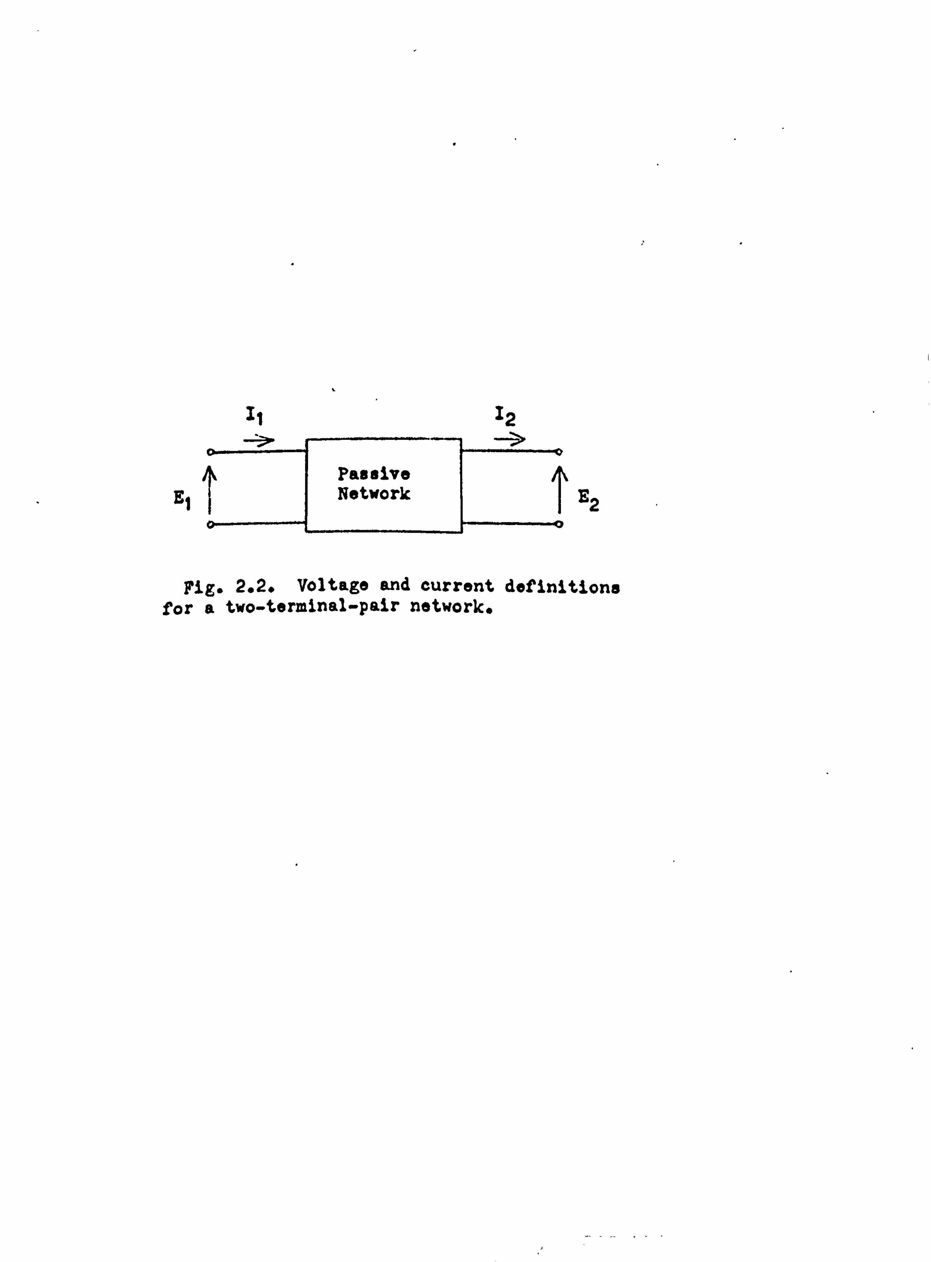
Iý 12
Passive N2 Network rk I
Fig. 2.2. Voltage and current definitions for a two-terminal-pair network.
22
all other respects. The external electrical behaviour of the
network can thus be expressed by means of any two linear rela-
tions involving the variables V1, Il, V21 I2. Six pairs of
such relations can be written expressing any two of these
variables as functions of the other two. Only one of these
six pairs, however, will be used extensively in this thesis.
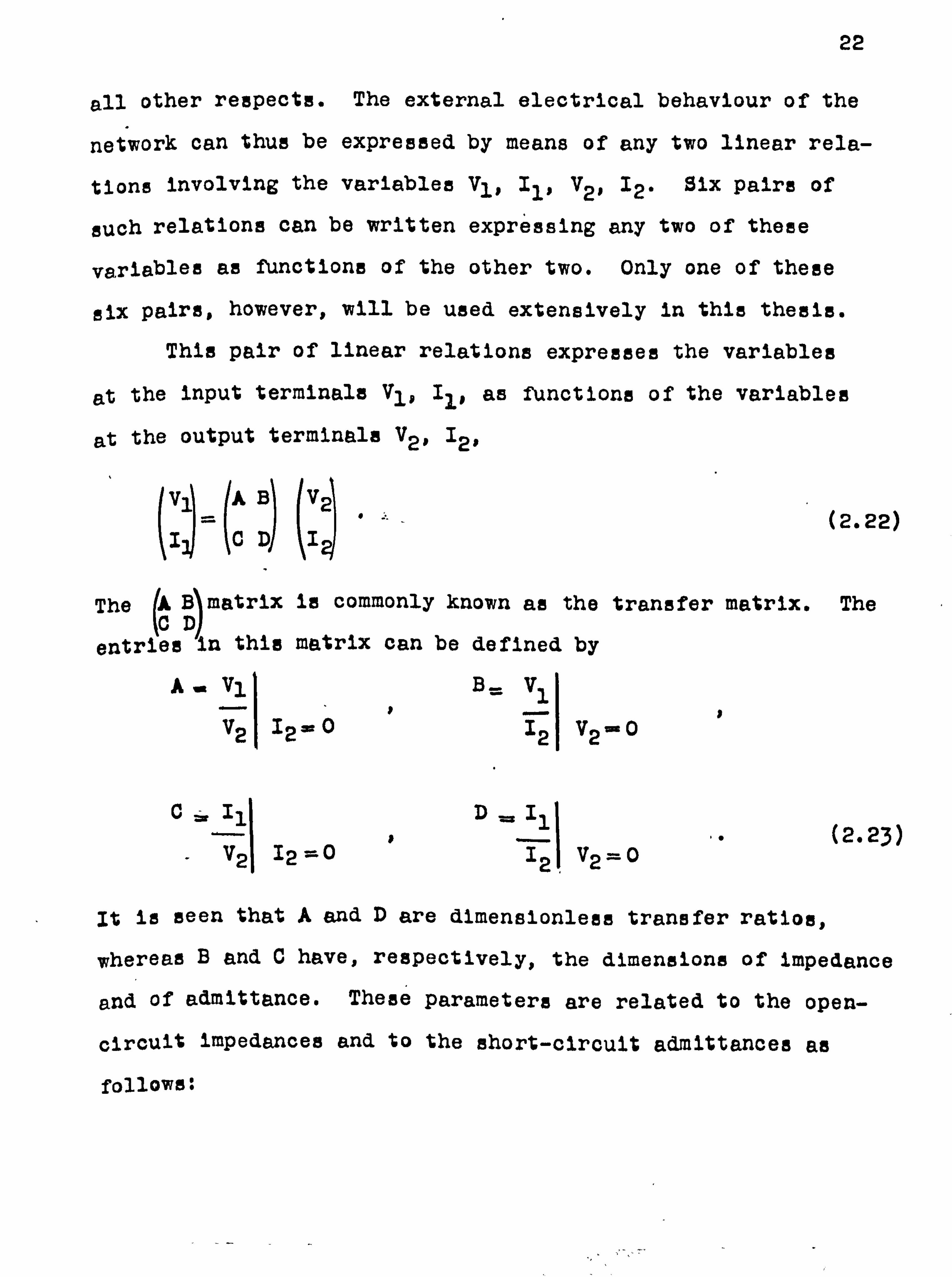
This pair of linear relations expresses the variables
at the input terminals V1, I1, as functions of the variables
at the output terminals V2, I20
V1 A B V2
I C D I (2.22)
The ýC B)matrix is commonly known as the transfer matrix. The D
entries in this matrix can be defined by
A. Vl B= Vl
V2 I2 =012 V2 =20
11 Il (2.23)
V2 12`2 02 V2 ̂ 0
It is seen that A and D are dimensionless transfer ratios,
whereas B and C have, respectively, the dimensions of impedance
and of admittance. These parameters are related to the open-
circuit impedances and to the short-circuit admittances as
follows:

23
Z11= ý, Z12= Z21=. l, Z22= D,
Y11= ., 712=72D=71j, 722= $,
det Y. 1 C, (2.24) det ZB
where A B1, = AD-BC=1. (2.25) IC D
The last relation states that only three of the four circuit
parameters are independent, as one would expect from the reci-
procity theorem.
In the particular case of symmetrical networks, that is,
of networks whose input and output terminals cannot be dietin-
guished by means of external measurements, the parameters
necessary to specify a two-terminal-pair network reduce to two.
One has, in fact,
711-722 Z11= Z22 'A=D. (2.26)
Reciprocal impedance networks represent another special case
in which the number of independent parameters is two. These
networks are characterized by the properties;
B' C, det Y= det Z =l, Y11= Z22, Z12- -Y12, Z11= Y220 (2.27)
The transfer matrix is particularly useful for the analysis
of cascaded networks, where the overall transfer matrix is given
by the product of the individual matrices in the appropriate

24
order. The individual matrices used in this thesis are given in
Fig. 2.3.
In this thesis only lossless networks terminated at either
end by resistors are considered, as shown in Fig. 2.4. Let all
impedances be normalized so that the source resistance is one ohm.
This is consistent with the definition of the voltage reflection
coefficient r considered in the previous section. In Fig. 2.4
it is desired to express as a function of A, B, C, D, and RL.
Combining the transfer matrices for RL and the lossless network
gives the result
1A B10 A+B BAB
CD1 1= CD C+D D
RL
From Eq. (2.24), Z= Z11- A/C. Recall now that the definition
of r was r. z_1 z1
Hence
A- WB
L r. .
(2.28)
(A+VL-c DRRL
This result is very important and will be used in the thesis
to derive the transfer matrix for a lossless network from the
voltage reflection coefficient.
In Fig. 2.4, the relationship between V. and VL can be
easily expressed in matrix form as

Series p---ýý---o Impedance 1Z Z0 1I
0
0 Shunt Admittance Y1y1
01
Y
Section of coeBl jZsinB1 Losaless Z
sinBl oosBl Transmission Z Line__ 1Z" Characteristic Impedance
$= Propagation Function
Zia Ideal 0-- Transformer
ii /a 0 0'
Fig. 2.3. Transfer matrices for several two port networks.
Is Re . 11L IL .0
Loseleoe ve 10 AB RL VL
D1 - Network
z, r
Fig. 2.4. Specific network configuration which is used in this thesis.

25
V$ 1 A
I 0 1 C e
B10 VL
D aL 1 0-= IL
where (L- 1/RL .
By straightforward matrix multiplication,
( BtC+(1D BtL +
C +(LD D0
ci's
which gives
VS
- A+GLB+C+GLD.
VL
The voltage insertion ratio is a function commonly
used to describe the overall behaviour of a network when
it is inserted between the source and the load. It is de-
(2.29)
(2.30)
fined as the ratio of the voltage across the load resistance
RL when the network is removed and replaced by an ideal
transformer to maximize power to the load, to the voltage
across RL when the transformer is removed and the network
inserted. It may easily be shown that the ideal transformer

26
should have a 1: V--L' turns ratio to deliver maximum power
to the load. Under this condition, let VL be the voltage across
RL.
To determine the ratio V3/VL , the ideal transformer
transfer matrix (Fig. 2.3) is used to obtain the result
Vý _11(010
VL
IS O0 'FRL a10
2 FyL JTTjý VL _ ýL 0,
or that Vg _2i.
(2.31)
VL
Now the above definition of the voltage insertion ratio may be
applied, giving
VLF 1 FLA
VL 2 t.
45 D . ý. B+ ARLC
. (2.32)
The square of the magnitude of the voltage insertion
ratio is called the insertion lose of the network. This quan-
tity may be regarded as the ratio of the maximum power Po that
the generator can furnish to the load (with the ideal transformer
connected between Rs and RL), to the power PL actually delivered
to the load through the network; i. e.,
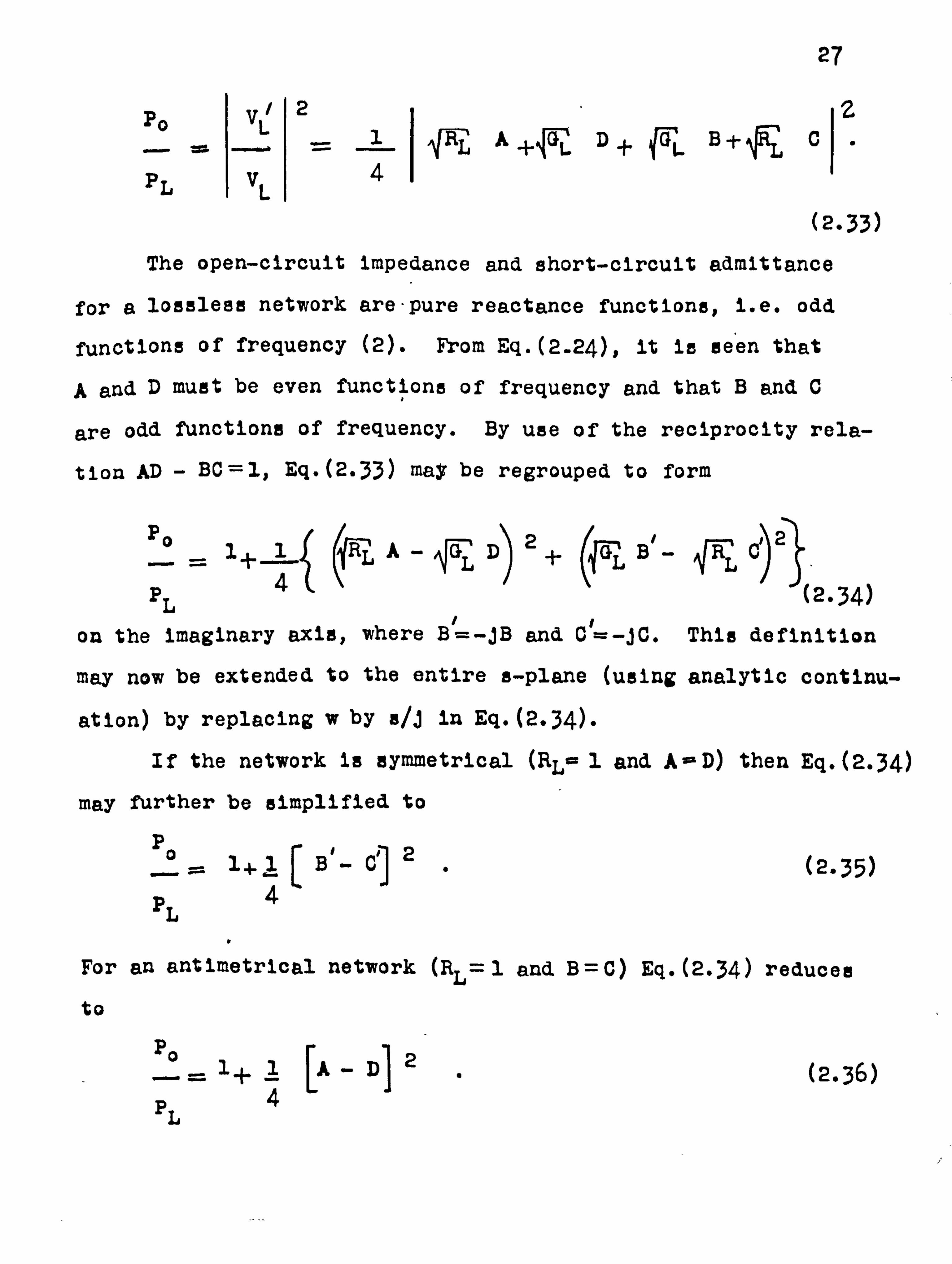
27
po Ivf2_ 2 'RL 1 A,
. 4G--Ll D+ UGB -t-
fIL C
PL IVL 4
(2.33) The open-circuit impedance and short-circuit admittance
for a 1oasleea network are-pure reactance functions, i. e. odd
functions of frequency (2). From Eq. (2_24), it is seen that
A and D must be even functions of frequency and that B and C
are odd functions of frequency. By use of the reciprocity rela-
tion AD - BC =18 Eq. (2.33) may be regrouped to form
Po
_ l+ 1A-D2+ (RB' 7L C, 2_ (FRL
A FGL
PL 4 (2.34)
on the imaginary axis, where B' -jB and Cý= -jC. This definition
may now be extended to the entire e-plane (using analytic continu-
ation) by replacing w by a/j in Eq. (2.34)"
If the network is symmetrical (RL= 1 and A- D) then Eq. (2.34)
may further be simplified to
p° 1. ý» 1 B'-0
PL 4 (2.35)
For an antimetrical network (RL =1 and B =C) Eq. (2.34) reduces
to
Po (' 1 ..... =
1-{- 1 [A - DJ 2 (2.36)
PL 4

28
2.4 The Darlington Insertion-Loan Syntheaie Technique.
2.4.1. Theory.
There are many different techniques for the realization
of a driving-point impedance. In general, different techniques
lead to different structures or arrangements of the elements.
If the structural form of the network is known in advance, and
the driving-point impedance satisfies certain realizability
criteria for that structure, then a synthesis technique can
hopefully be devised to obtain the element values in the structure
from the input port driving-point impedance. This thesis is
concerned only with the structure shown in Fig. 2.4 (in which the lossless network is a cascade of simple networks) for which the insertion loss is specified. The synthesis technique which is used for this structure is called the Darlington insertion-
loss method (3), a description of which now follows.
Since the ABCD network in Fig. 2.4 is assumed lossless,
the transmitted power to the load RL is the difference between
the available power and the reflected power. Therefore, in
Fig. 2.4, the insertion loss is given by
Po
_1 -pL 1-
Ir'(jw) I2 (2.37)
In modern two-port filter design it is usually the insertion
loss as a function of frequency which is the design specification.
29
In section 2.2 it was shown that r(s) is a bounded real
function, which implies that when a is real r (e) is also real,
and thus complex zeros or poles of T '(s) must occur in complex
conjugate pairs. Consider a pair of complex zeros (or poles) of
r(s). Then r (-a) contains images of these zeros about the im-
aginary axis, and the four zeros in r (s) r (-a) have (quad-
rantal) symmetry about the real and imaginary axes. Multiplying
these zeros together yields the factor
(s2tastb) (e2 - aa+b)_
s4+- ce2 +d,
which is an even function of s2, or of w2 if a= jw. Similarly,
a zero (or pole) ofF (s) on the real axis will give rise to a
mirror image zero in r(-s), resulting in r(s) r'(-a) having a
factor
a2-a,
which is again an even function of w2. Thus, a necessary require-
ment on the numerator and denominator of r(s) r'(-a) is that
they be even functions of w when a= j w. It follows that Ir(jw)12
must be of the form
Irjw2= M(w2) < 1. (2.38)
W(w2)
From Eq. (2.37), the insertion loss when s= jw is given by
Po 1 W(w2) _>1.
PL 1- M(w2 W(w2) - M(w2)
W(w2)

30
Letting N(w2)_- W(w2) - M(w2), this equation may be rewritten as
PO
_I+ M(w2 Z 1, (2.39)
FL N(w2)
where M and N have non-negative values on the w axis.
The next step in the Darlington synthesis method is to
expand the definition of lrL'w) I2
to the entire e-plane by
analytic continuation (replacing jw by a). Eq. (2.38) may now
be written
r (a) r (-s) = M(-152) (2.40)
M(-a2) + N(-a2)
How may Eq. (2.40) be factored to recover r' (s)?
The roots of the denominator may be found from
M(x) -- N(x) - 0, (2.41)
where x- -s2. Since Eq. (2.41) has real coefficients, complex
zeros of this polynomial will be in complex conjugate pairs,
a pair giving rise to a factor
x2 t ax +b =
a4± a82+ b,
where b >0.
This factor may be shown to represent a quartet of
r(s) r (-s) poles (having symmetry about the real and imaginary
axes). Since r (s) must be a bounded real function (Eq. (2.20)),
the two lhp (left half plane) poles must be chosen for r' (s).
Other factors of Eq. (2.41) will be of the form (x ± a), a> 0.

31
The factor (x + a) results in two poles, at e=-4, T. Again, since
r(s) must be bounded real, the lhp pole is chosen for r (a).
Finally, a factor (x - a) implies that two poles of f (a) r'(-s)
are on the imaginary axis of the s-plane. In turn, Egs. (2.38)
and (2.37) show that at these zero points Po/PL a 0, which, by
the construction of Po/PL in Eq. (2.39) (M(w2) and N(w2) are
non-negative), is impossible. Thus a factor (x - a) will not
appear in the factorization of Eq. (2.41). The imaginary axis
is seen to be a "sorting" boundary for the denominator roots of
Eq. (2.40), with the lhp zeros forming the denominator of r (a).
The numerator roots are determined from
M(x) = 0, (2.42)
where X_ -a2. Complex roots of Eq. (2.42) occur in complex
conjugate pairs, a pair of which yields the quartet of roots
s4±as2 +b, b) 0.
Either the lhp pair or the rhp pair may be chosen for r (e),
the other pair going to r (-a). Factors of the form (x i- a) ,a70, have roots at a=±rä , and either may be chosen for a zero of
f "(a), with the other zero going again to r (-a). Finally,
factors with the form (x - a) have roots at a± jýa'. Since
M(w2)> 0, these roots must be of even multiplicity, ie. (x - a)2k,
where k is an integer. Then r' (s) and r'(-e) have the factors
(x - a)k.
Thus, in general, many different selections are possible
for the zeros of r (a), each leading to a different network
32
having the same insertion loss. If all of the zeros of M(-e2)
are on the imaginary axis, however, it is seen that the factori-
zation of (^(s) r'(-a) in Eq. (2.40) is unique and only one network
will emerge. Such will be the case for most of the networks
considered in this thesis. '
The final step in the Darlington technique is the realiza-
tion of the lossless network from r (a). Although many different
methods may be used, the method used in this thesis is to re-
cover the transfer matrix for the lossless network from r
(Eq. 2.28). Then elements are extracted from this transfer
matrix according to the desired structure. The method is to
premultiply (or postmultiply) the transfer matrix by the inverse
matrix of the desired element and then require the resulting
transfer matrix to be of lower degree. This requirement will
determine the element value. It turns out that this require-
ment leads to two independent equations for the element value,
which is very useful when estimating the inaccuracy (due to
round-off errors, etc. ) in the numerical calculations.
2.4.2. An Example of the Darlington Method: The Butterworth
Specification.
A maximally flat function is one which has all of its
zeros coincident at one frequency point, commonly referred to
as the center frequency. A maximally flat function g which
possesses n zeros at the center frequency wo has the property
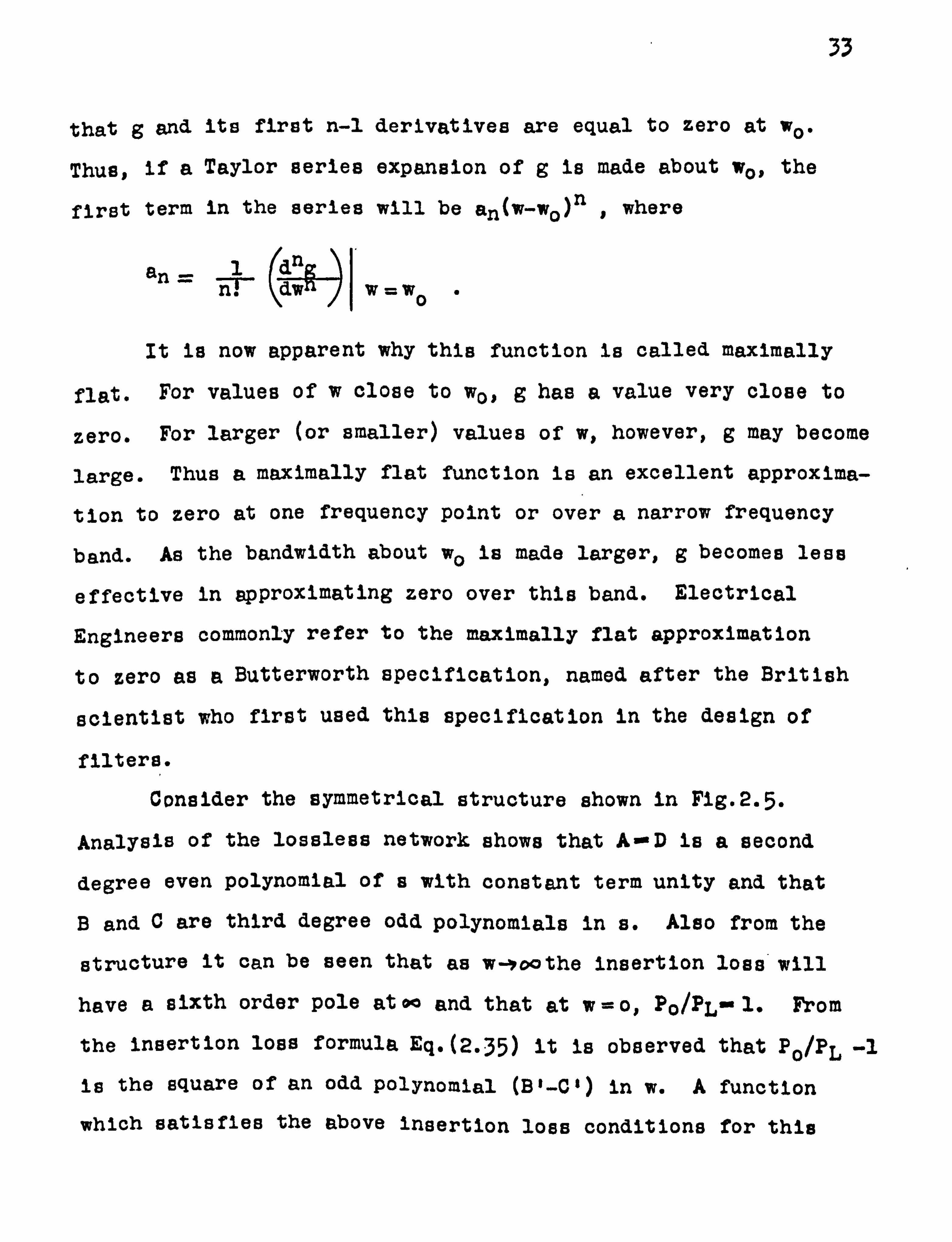
33
that g and its first n-i derivatives are equal to zero at wo.
Thus, If a Taylor series expansion of g is made about wo, the
first term in the series will be an(w-wo)n , where
an_ 1 do n. dw w= wo
It is now apparent why this function is called maximally
flat. For values of w close to wo, g has a value very close to
zero. For larger (or smaller) values of w, however, g may become
large. Thus a maximally flat function is an excellent approxima-
tion to zero at one frequency point or over a narrow frequency
band. As the bandwidth about wo is made larger, g becomes lese
effective in approximating zero over this band. Electrical
Engineers commonly refer to the maximally flat approximation
to zero as a Butterworth specification, named after the British
scientist who first used this specification in the design of
filters.
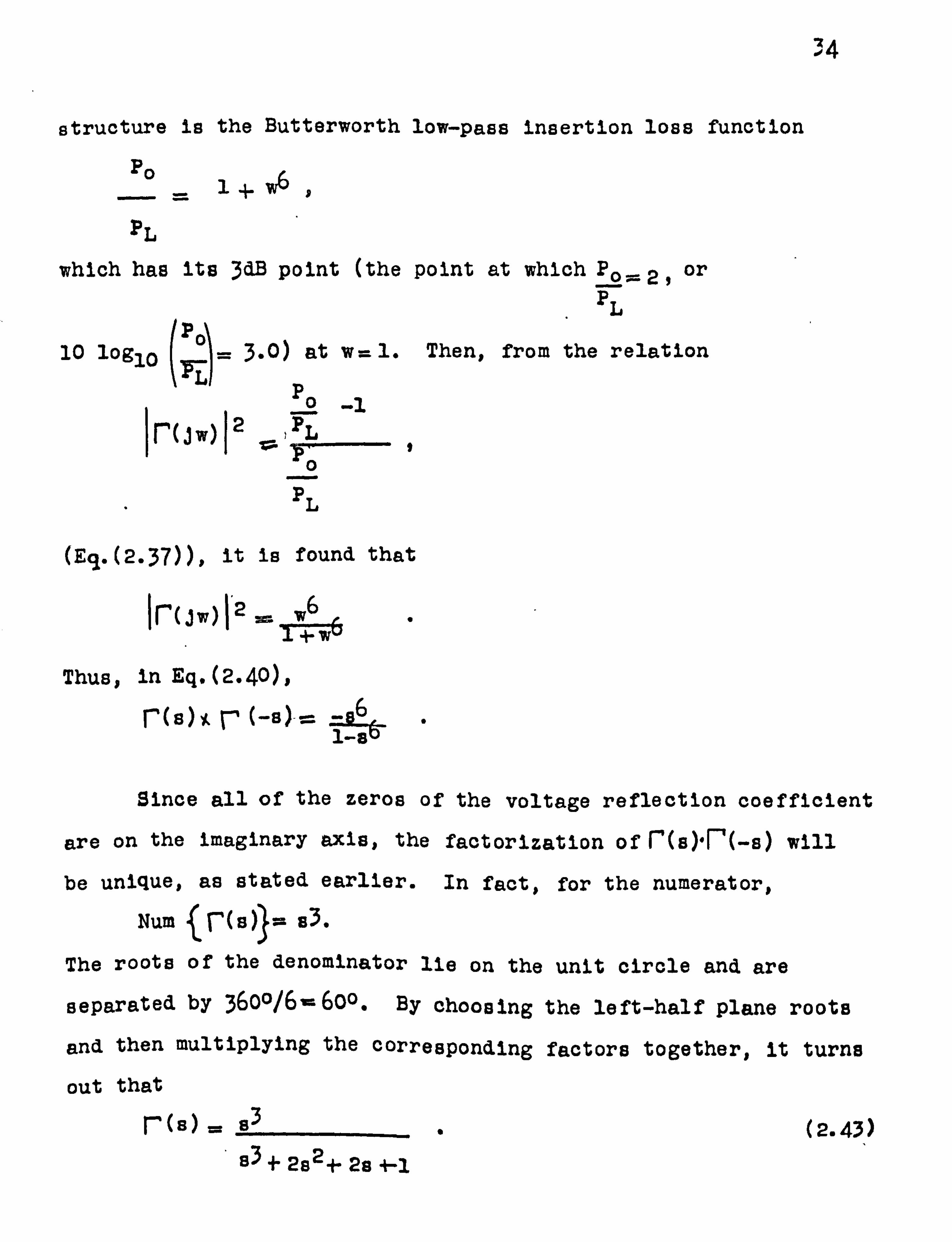
Consider the symmetrical structure shown in Fig. 2.5.
Analysis of the lossless network shows that A-D is a second
degree even polynomial of s with constant term unity and that
B and C are third degree odd polynomials in s. Also from the
structure it can be seen that as w-voo the insertion loss will
have a sixth order pole at oo and that at w =o) Po/PLC 1. From
the insertion loss formula Eq. (2.35) it is observed that Po/PL -1
is the square of an odd polynomial (B'-Cl) in w. A function
which satisfies the above insertion loss conditions for this
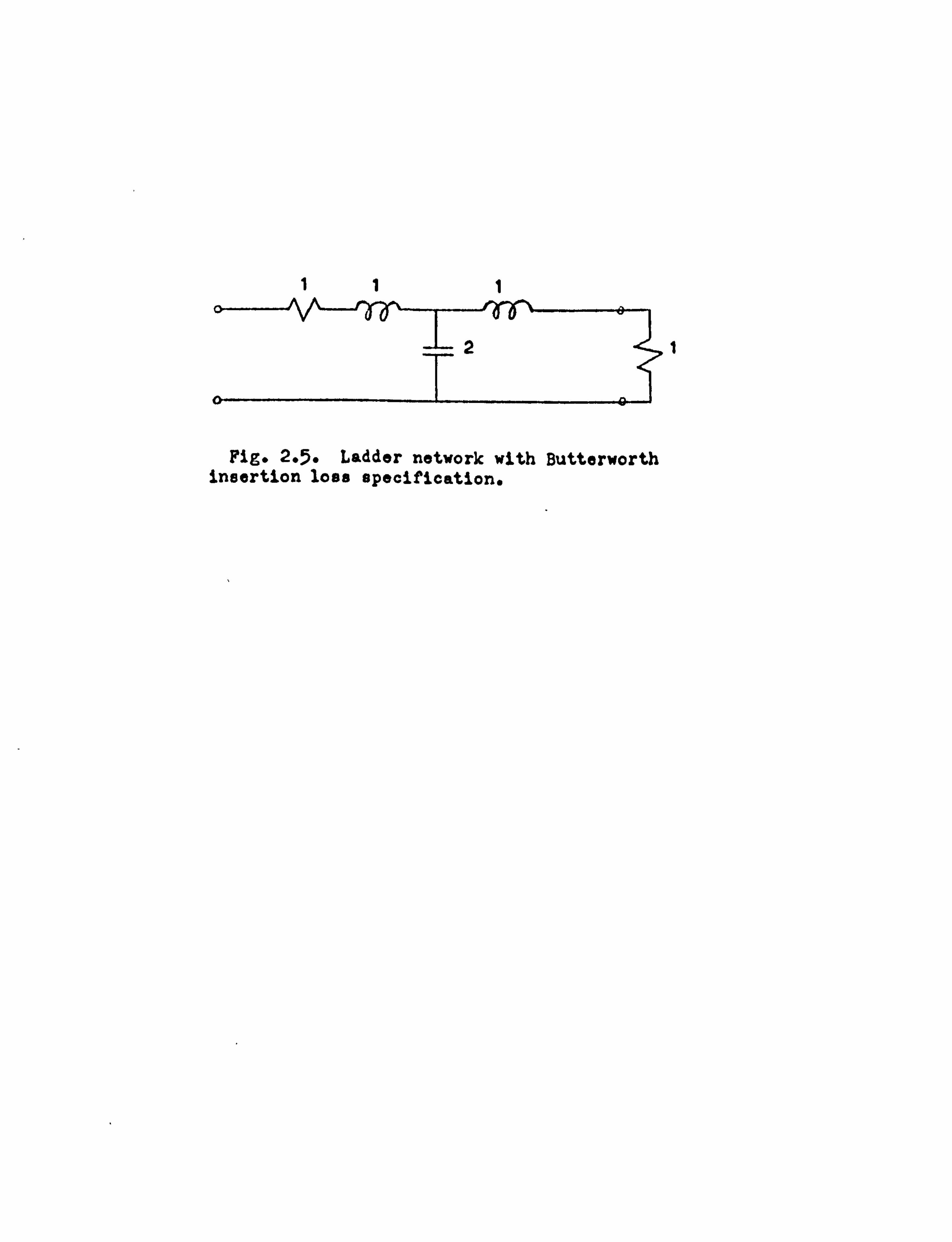
0 rp -- --
Fig. 2.5. Ladder network with Butterworth insertion lose specification.
-4
structure is the Butterworth low-pass insertion loss function
Po
= 1+ w6
s PL
which has its 3dB point (the point at which Po ^ 2, or
PL P
10 log10 = 3.0) at v= 1. Then, from the relation -O) LP
O I row) I2
V. 'PL ö
pL
(Eq. (2.37)), it is found that
Ifl(jw)L2 _ W6 Thus, in Eq. (2.40),
r(s)t r (-8)-= " Since all of the zeros of the voltage reflection coefficient
are on the imaginary axis, the factorization of r'(s)'r'(-s) will
be unique, as stated earlier. In fact, for the numerator, Num {(''(s)}- 0.
The roots of the denominator lie on the unit circle and are
separated by 3600/6= 600. By choosing the left-half plane roots
and then multiplying the corresponding factors together, it turns
out that
r(s) = 83 (2.43) s3 + 2s2+ 2s +-1

35
Recall that the definition of the voltage reflection coefficient
is r+_ (A-D _
(8-C A+ -4- B1
(2.28)
Hence, multiplying both numerator and denominator of Eq. (2.43) by
two (so that the constant term in A=D is one), it is found that
for the Ioslese network
AB 2x2+ 1 2s3+ 2s
CD 2s 282+ 1
Starting at the left-hand side of this network, a series
coil will first be removed. The inverse matrix for a series coil
is easily shown to be
1 -La . 01
Therefore,
1- -Ls)-(2a 2+1 2x34- 23
01 4s 2s2+ 1=
282 -2Ls2+1 283 - 2Ls3+ 2s - Ls A (2.44)
2s 262+ 1CD
The requirement that this matrix be of lower degree results in
two equations:
1) A: 202 - 2Ls2=0, from which L -1.
2) H: 2s3 - 2Ls3 = 0, from which La1. i
Thus the accuracy checking feature of this matrix decomposition
method is brought to light. After L is removed, the transfer

36
matrix will be
18
2a 282 -1- 1
Next a capacitor Cl will be removed.
shunt C1 is
10 (-Cjs 1
Therefore,
lo )C-scil
s
0
8 ý.
2$2+ 1 2s-sCl
(2.45)
The inverse matrix for a
8
2s2_C182.1-1 "
By inspection, C1 = 2. Since the network is symmetrical (A=D),
the final series coil has an inductance of 1 (henry). The final
network with element values is shown in Fig-2-5. After removing
all of the elements, the transfer matrix should be the unit 1o
matrix o 1), which may be viewed as a 1: 1 transformer. This
transformer may be omitted from the cascade, if desired. The
realization has thus been achieved.
The above method of determining the element values from f
is not the "quickest" one (a continued fraction expansion of
A/C results in the same element values), but it is a very
straightforward method and gives accuracy information as the
synthesis proceeds, and is useful in other types of networks
to be discussed later.
37
2.5 The Scattering Matrix.
The extension of the insertion loss concept to an n-port
network will now be considered. It is remembered that the
insertion loss description of a two part network is meaningful
when the network is terminated at either end by a finite non-
zero impedance. If the network has an open or short-circuit
on either end then some other description (such as the voltage
or current insertion ratio) becomes more appropriate. This
same fact holds true for an n-port description function. All
of the n-pdrt networks considered in this thesis are resistively
terminated. Hence the scattering matrix description of the
n-port will be developed with this restriction.
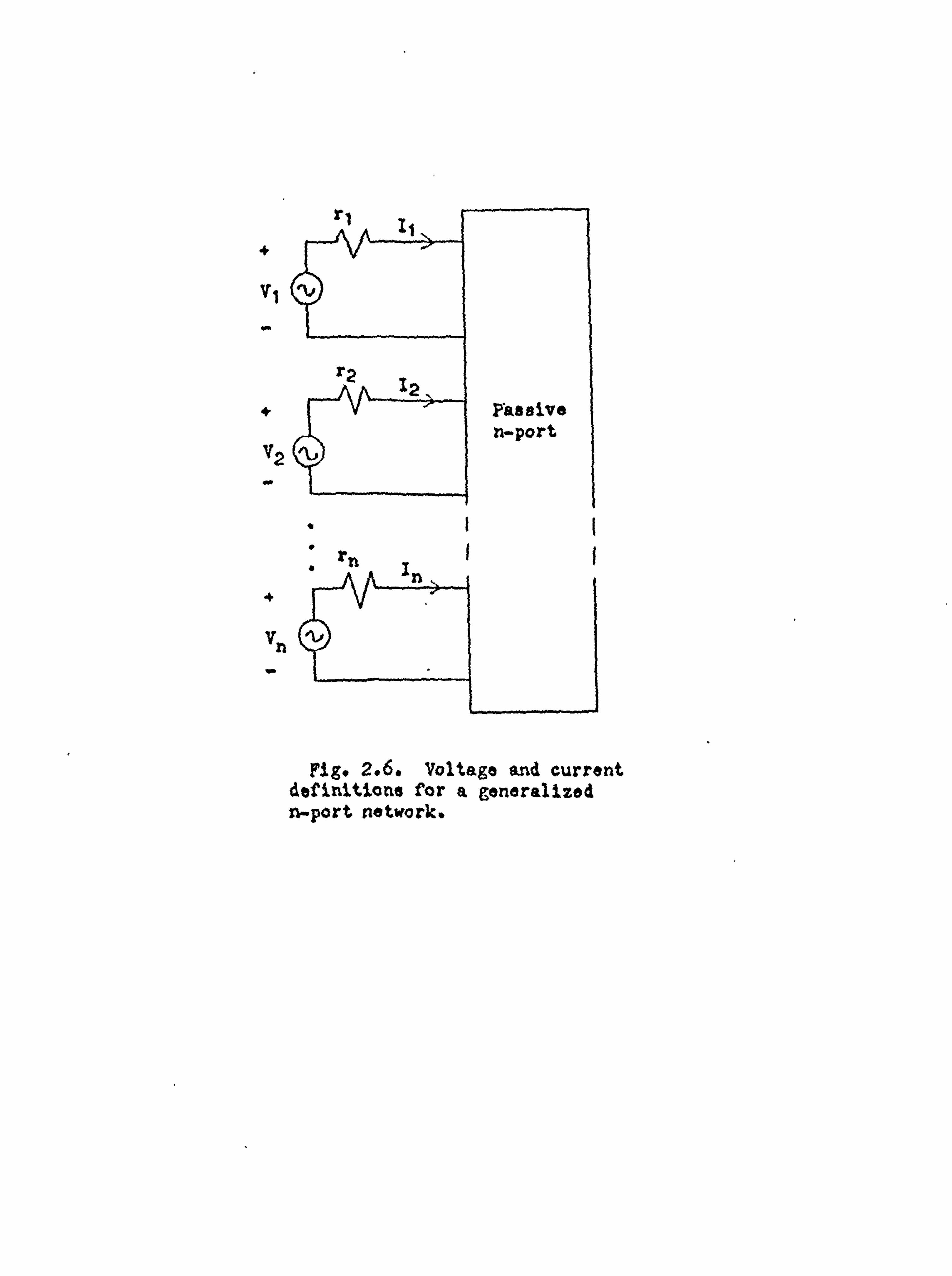
Consider the n-port shown in Fig. 2.6.
Let (V) and (I) be 1Xn column matrices defined by
(v)(2) Vi (2.46)
I2
v
and let (A), (B), (Cýý, (D), and (X) be defined as nX n matrices.
The most general linear relationship between (V) and (I) is given
by (A)
M+ (B) (I )) _ CX) ((c)(v)+
(D) (I)
Specialized forms of Eq. (2.47) may be derived.
0 (2.47)
(B) = (C) = 'no
and (A) (D) = 0,
For instance, if
(2.48)
4
VI M
V2
"+i rn
I n
vn
Fig. 2.6. 'Voltage and current definitions for a generalized n-port network.

38
where 0 is the null matrix (all entries are zero) and In is the
unit matrix of rank n (entries on the major diagonal are 1 and
zero elsewhere), then (X) turns out to be the (Y) or short-
circuit admittance matrix. On the other hand, if
(B) = (C) = 0,
and (A) = (D) = In, (2.49)
then (X) is equivalent to the (Z) or open-circuit impedance matrix.
Now, to extend the concept of insertion loss to an n-port
network, in Fig. 2.6 let
power delivered to rj by Vk with
SkI inserted 9
(2.50) ,I
maximum power delivered to rj by Vk with
optimizing transformer inserted
where the. (X) matrix in Fq. (2.47) is now defined as the (8)
matrix, and Sjk is the entry of the jth row and kth column.
By comparing Eqs. (2.50) and (2.33) it is seen that ISjkl2= lPo/PL
for a 2-port, and so this is the-. connecting link between insertion
lose and the (s) matrix (which is now called the scattering
matrix) for an n-port.
The question now arises as to what definitions to give
the (A), (B), (C), and (D) matrices so that definition (2.50)
holds true for the n-port. To simplify matters, it is first
assumed that (A), (B), (C), and (D) are diagonal matrices (all
entries not on the major diagonals are zero). Further, let
(A) _ (C)= 9 diag Rj2 2 diag Rj T
(2.51)

39
and (B)-(D). ;I diag Rý
1 where (diag R17) is a diagonal matrix of degree n and the R,
are real, positive numbers called the port normalizing numbers.
With these definitions, first a restriction on the scattering
matrix due to the passivity of the n-port will be derived, and
then the quantities on the right side of Eq. (2.50) will be de-
veloped to verify the definition of the scattering matrix.
Let Eq. (2.47) be written in the form
(b)=`(8) (a) (2.52)
Then from (2.51) and (2.47), 1
bj= 2(Rj T Yj - Rj'I Ij ), (2.53)
). and aj 2(R Vj -t' jý. ' Ii
Solving for (V) and (I),
(V) = (diag R, 3-) (a) -t-(b) ) (2.54
(I) _ (diag R, "; ) (a_b) ).
Now since Vj and Ij in Fig. 2.6. are assumed to be sinusoidal
time waveforms, the power entering the n-port through port j
=Re (Vj*')
, where the asterisk indicates the complex conjugate.
The total power entering the n-port is given by
P= (Re Vj Ij) = (V)(I), (2.55) jl
where the tilda means the transposed (making the column matrix
into a row matrix) complex conjugate. From (2.54),
40
(ý')- ((i)
+ (bj) (uag
Rj j
and hence
P -Re (( ) ýI)) Re
((ä) + (b))
SRS ýVL)+(b))
((a)_(b)}
(2.56)
(diag Rj*)(diag Rid`) ((a)_(b)
wz(ä)(a) - (b)(b), (2.57)
since the real part of C)(a)-(a)(b) is zero.
From Egs. (2.57) and (2.52),
("a) (OL)- (cr. s)c)) (8)(a) C (a) In (^ý)(s (a). (2.58)
Now if the n-port is passive, P>-O,, and the matrix (1
n-4)(8)
must be positive semidefinite (`). If this is true, then
3, - (T) (s) 2ý 0, (2.59)
is a restriction on the scattering matrix for a Passive n-port.
Furthermore, if the n-port is lossless, then P= 0 and Eq. (2.59)
reduces to
(ß) (ß) =I (2.6c) This result la an important conclusion, and is commonly referred
to as the unitary condition for the scattering matrix of an
n-port. This condition will be used in the directional Coupler
work later in the thesis.
Now it is necessary to show that the scattering matrix (8)
that has been derived does indeed satisfy the definition 12.50).
In deriving Eq. (2.59) no restrictions have been placed on the R,
in the (A), (B), (C), and (D) matrices other than that they be
real, finite, non-zero, and positive. Thus there is no connection
41
between the rj in Fig. 2.6 and Rj so far. Certain convenient
properties arise when the rj are set equal to the port normal-
izing numbers Rj, however, and this equivalence will be assumed
in the following derivation.
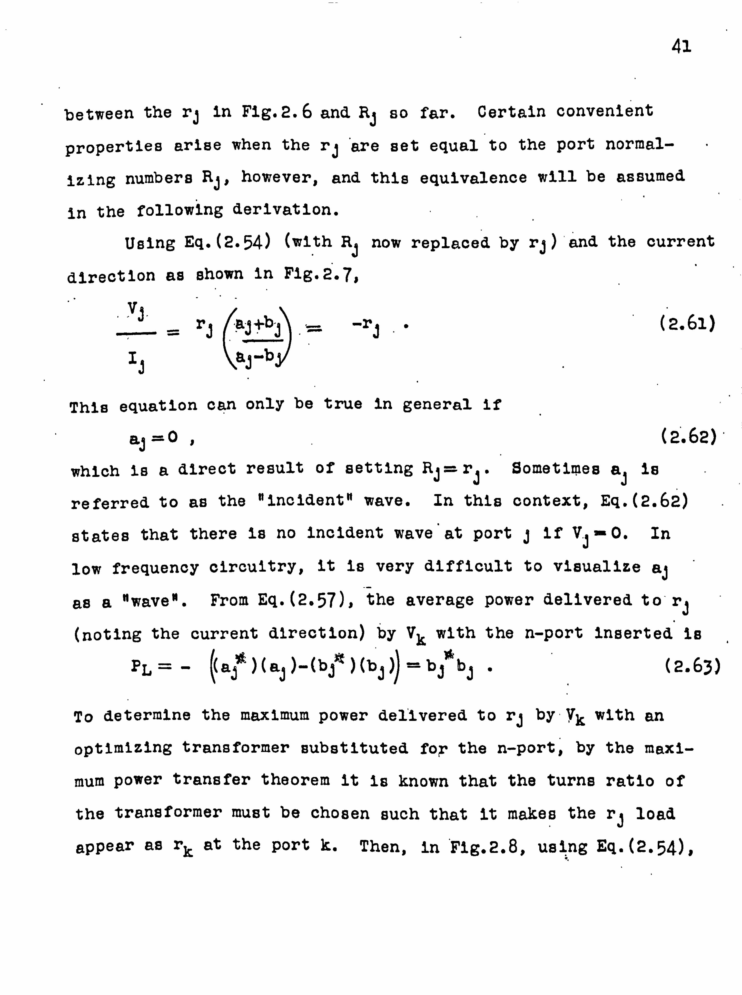
Using Eq. (2.54) (with Ri now replaced by rj) and the current
direction as shown in Fig. 2.7,
vj r, (aj+bj' _ -ri
I, a, -b
(2.61)
This equation can only be true in general if
aj=0 , (2.62).
which is a direct result of setting Rj= rj. Sometimes a, is
referred to as the "incident" wave. In this context, Eq. (2.62)
states that there is no incident wave at port j if Vj - 0. In
low frequency circuitry, it is very difficult to visualize aj
as a "wave". From Eq. (2.57), the average power delivered t o'rj
(noting the current direction) by Vk with the n-port inserted is
PL= - ((aj )(aj)-(bj )(bj)) =bj bj " (2.63)
To determine the maximum power delivered to rj byVk with an
optimizing transformer substituted fox the n-port, by the maxi-
mum power transfer theorem it is known that the turns ratio of
the transformer must be chosen such that it makes the rj load
appear as rk at the port k. Then, in 'Fig. 2.8, using Eq. (2.54).
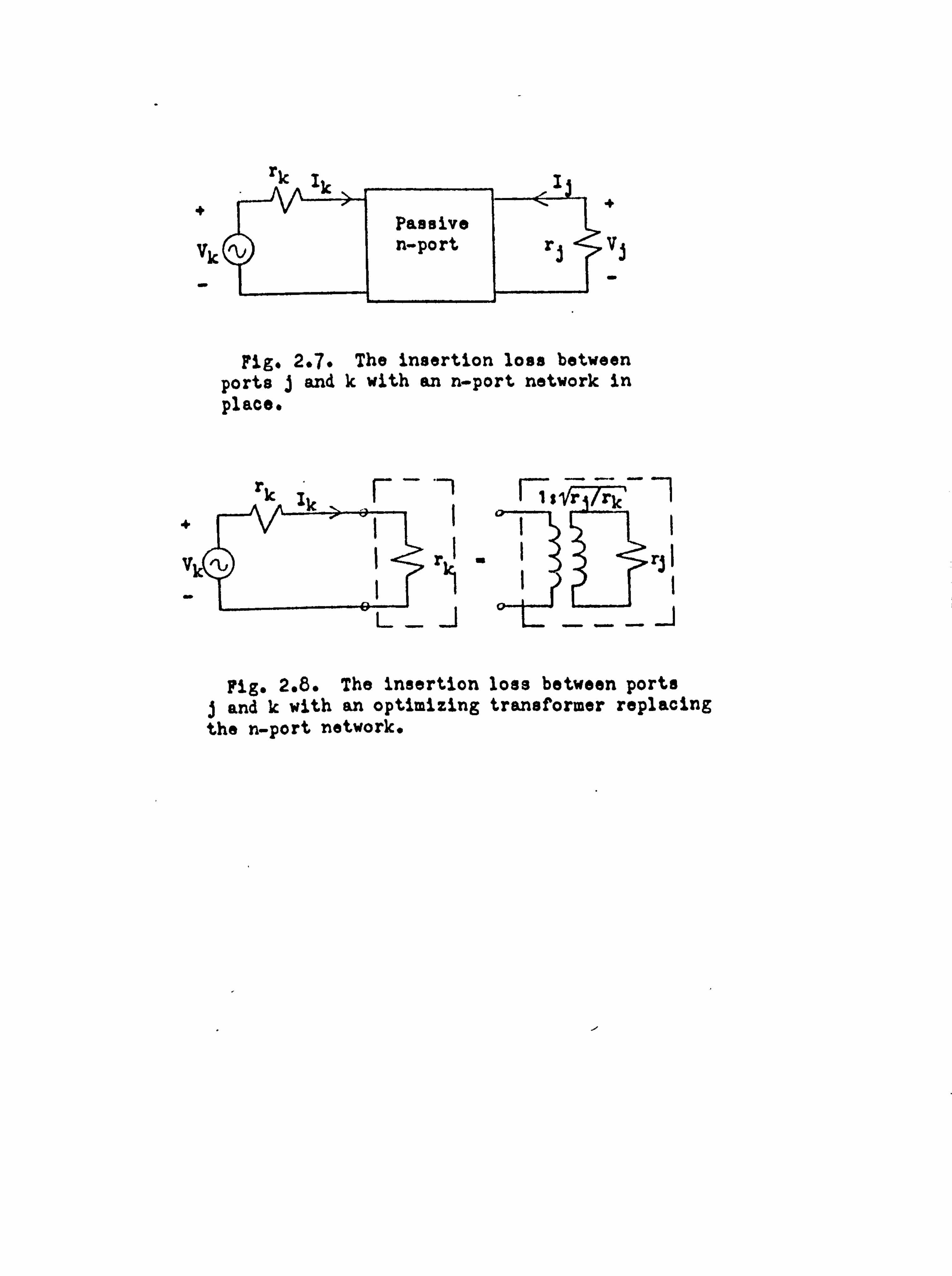
rk Ik I
Passive vk "J n-port rj
4Vi
Fig. 2.7. The insertion loss between ports j and k with an n-port network in place.
rk ik
+I
V 'L rl i
L_J
ý1s ri Tr-k""
i
rj
Fig. 2.8. The insertion loss between ports j and k with an optimizing transformer replacing the n-port network.

42
1 Vl 2Vk g rk (ak+- bk) ,
(2.64)
and Ik = Vk
"-m rk-' (ak - bk)
2rk
Thus,
ak .. bk (2.65) 7 or bk= 0.
ak"bk
Historically, bk has been called the "reflected" wave from
port k. Eq. (2.65) shows that there is no reflection at a
matched port. Now the power delivered to r, in Fig. 2.8 is
'V PA = Re (V1 Ik) akkak (2.66)
Finally, by using Eqs. (2.66), (2.63), and the fact that bl s Sjkak,
it is seen that the definition (2.50) is true, as was asserted.
It will now be instructive to show that the scattering
matrix for a passive n-port always exists and is symmetric
(giJWr. S, i)(5). Consider the augmented n-port in Fig. 2.9.
In general it can be shown that the (Y) matrix for the augmented
n-port always exists, although it may not do so for the original
network. The idea behind this augmentation is to express (ß)
for the non-augmented n-port in terms of (Y) of the augmented
network, which is known to exist. The Rj are, as usual, chosen
as the port normalizing numbers for the non-augmented network.
Let (YA) be the (Y) matrix for the augmented n-port.

r Au enteil u-pir't
-
Axigial z-port
Vi v n-porL
.. 1
J "1 Rn
2. g. Tht oagm. nted network used to Q manistrata the existvnalm of the scattering xatxlx.
43
Then, by definition,
(I)' (YA)(V)" (2.67)
Inspection of Fig. 2.8 gives the relation
Vi =V1+I, R, ,
or (2.68)
(V) _ (V) + (diag Rj)(I).
By using Eqs. (2.67) ,
(2.68) , and (2-54)s it is found that
(I) _ (YA) (V) 1- (diag R M) )
j (YA) (diag Ri ) ((a) - (b)) f (diag Rjk)
((a)_(b))
=(YA) 2(diag Rjk) (a)). (2.69)
But also (I) _ (diag RJ-i) (a)-(b)
, (2.70)
from Eq. (2.54)" Thus,
(diag R j-') (b)
((dias Rj 'E)-2(YA) (diag R 1) (a).
, (2.71)
which yields
(b) w ln-2(diag Rý ) (YA) (diag Rý *) (a)
(5)(a). (2.72)
Therefore, since (YA). exists (by assertion), (8) exists for a
passive n-port.
It is also known that if (Y) exists for a passive n-port
containing only reciprocal elements, then (Y) is symmetric
(Yij vRYji). From (2.72) it is obvious then that
9ij W. 8ji " (2.73)
This symmetry property, the existence theorem, and the unitary
condition for a lossless network are the main results which are
used in chapter 5.

44
2.6 Determination of Phase From A Magnitude Specification.
In chapter 5 it will be necessary to determine the phase
of an analytic function at one frequency point given the magni-
tude of the function along the frequency axis. The following
discussion is directed towards this end.
An important result from analytic function theory is the
Cauchy integral law, which states that
(s)ds . 0, (2.74) ��C
where C is a simple closed curve in the s-plane, and F(s) is
an analytic function of s in and on C. Now assume that F(s)
is analytic when6'0, and that F(o0) is finite and single-
valued. Let
G(s) F(s e-, wl
(2.75)
and consider the curve C shown in Fig. 2.10. It is seen that
the Cauchy integral law may be invoked for this G and C, and
therefore J a(s)ds«mo. (2.76)
The contribution from path ADD to this integral is 1r
fa(s)ds- 2 F(Reje) jReie de.
AHD Re, e
_, wl
As
fa(a) ds=, F(oo) d®7rF(vo). (2.77)
_2 ABD rr

x
jM
Q
Fig. 2.10. The integration contour used in Eq. (2.76).
Magnitude Magnitude
1. o
. 1o
. ot
.ý1 10
(")
1.0 . 10
. 01 w
(b)
M
Fig. 2.11. (a) Straight line approximation to IF(jx)I
and (b) the decomposition of (a) into semi-infinite segments.
\ý

45
The contribution to Eq. (2.76) from path EF is
i f G(s)ds = F(jwltreie)jreiede
EF 'fi re 2
-7
=j F(jwi+ reie)d8 .
As r-s 0, e
f(s)ds = -jWF(jwl). (2.78)
EF
Thus Eq. (2.76) becomes 00
F( w dw mj 1r(F(04 - F(iwi) , (2.79)
J ß-W1 -00
where co F( w thy _ ihn
wr F( w dw
,. F( w dw
. r. -o0 f
w-wl w-wl _n0 -oo wltr
Now let
F(s) _ R(s)+, X(s), (2.80)
where R and X are the real and imaginary parts of F. Using this
definition, the real part of Eq. (2.79) becomes CO
1 R(w dw xa X(w1) -x( 00 (2.81) "Tr w-wl
-00
Eq. (2.81) shows that once R(w) is specified, X(w) is uniquely
determined. It is sometimes referred to as a Hilbert transform.
By algebraic manipulation, it can be shown(6). that
Eq. (2.81) is equivalent to
46
eo
X(wl) =1 dR 7r du
-00 where
u= 1nwl `wýf
in coth Iul du, 2
(2.82)
(2.83)
Next, H(s) is defined by H(s) = In F(s) = In IF(8)I+jP(8),
where P=tan-'(, R is the phase of F(s). Then Eq. (2.82) becomes
00 (wl) ^1 dln F( w
(ln coth
Ju d u. (2.84) Ir u2
-0,0 Eq. (2.84) is the main result for this section, and shows how
the phase of an analytic function can be determined from the
magnitude on the w axis.
Unfortunately,. -the integral in Eq. (2.84) is very difficult
to evaluate for most cases of practical interest. An approxi-
mation can, however, be made(7), which gives satisfactory results.
First, IF(jw)I
is plotted on log-log graph paper, with both the
w (horizontal) axis and the IF(jw)I
axis having the same logar-
ithmic scale. The number of logarithmic cycles for both axes
is made large enough'to show the principal variations in INext,
jF(iw)I is approximated by a number of straight ling
segments, (Fig. 2tll (a)). This approximation can be regarded
as the superposition of straight lines, each starting on the
w axis at wi (the "break point"), having a slope ki, and ex-
tending to infinity (Fig. 2. l1 (b)). For each straight line,
Eq. (2.84) gives the result
47
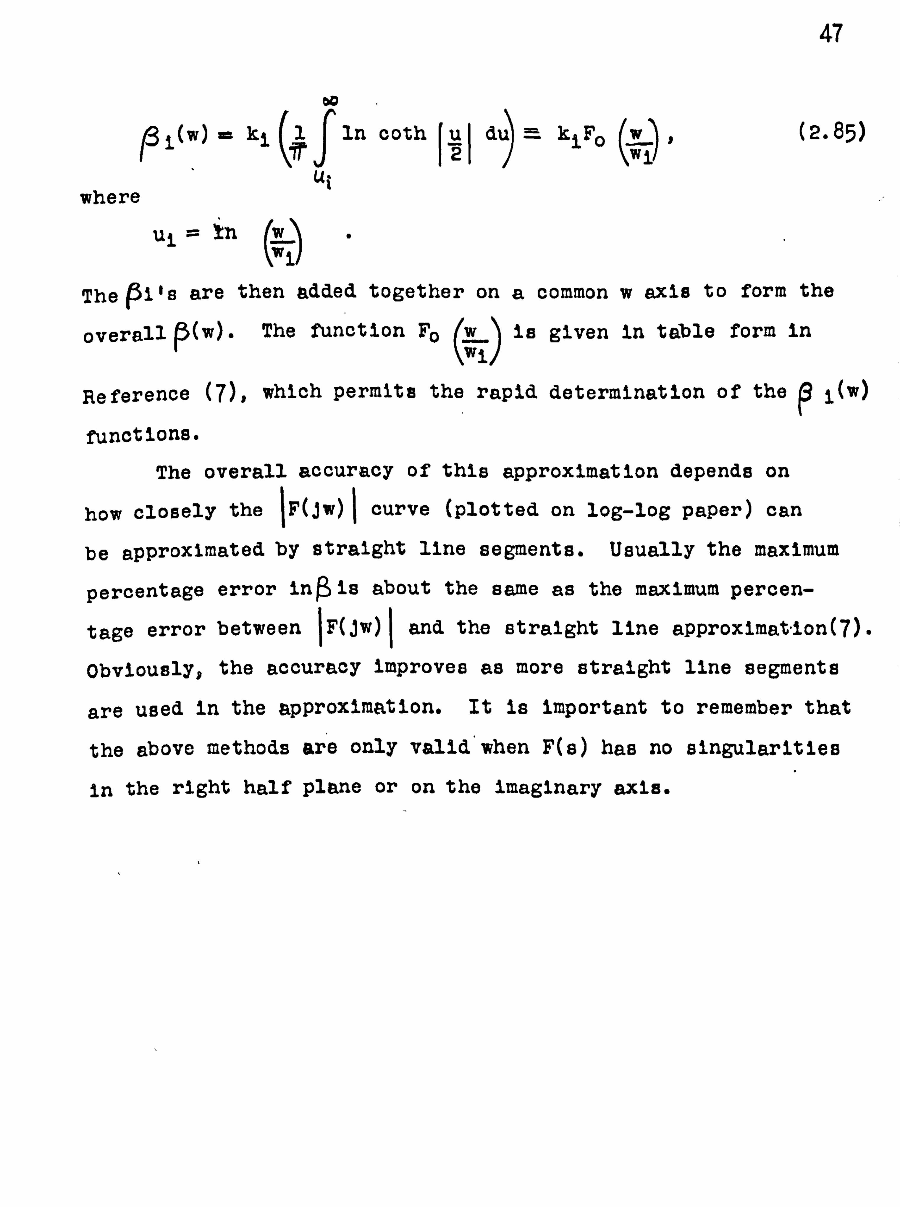
oa P i(w) = ki In coth
2( du = k1Fo iw)
, (2.85)
I/
Ui where
ui=T wl
The Pi's are then added together on a common w axis to form the
overall 13(w)" The function Fo (MW, -) is given in table form in
Reference (7), which permits the rapid determination of the Q i(w)
functions. 1
The overall accuracy of this approximation depends on
how closely the IF(jw)I
curve (plotted on log-log paper) can
be approximated by straight line segments. Usually the maximum
percentage error in ß is about the same as the maximum percen-
tage error between IF(jw)I
and the straight line approximat"ion(7).
Obviously, the accuracy improves as more straight line segments
are used in the approximation. It is important to remember that
the above methods are only valid when F(s) has no singularities
in the right half plane or on the imaginary axis.

48
Chapter 2 REFERENCES
1. Brune, 0.: "Synthesis of a finite two terminal network
whose driving-point impedance is a prescribed function
of frequency", Journal of Maths. & Physics, 1931,
10, p. 191.
2. Ragan, G. L.: "Microwave Transmission Circuits". MIT Radia-
tion Laboratories Series, McGraw-Hill, 1948, P"550.
3. Darlington, 8.: "Synthesis of reactance four-poles which
produce prescribed insertion loss characteristics,
including special applications to filter designs".
Journal of Maths. and Physics, 1939,18, p. 257.
4. Weinberg, L.: "Network Analysis and Synthesis". McGraw-
Hill, 1962, p. 258.
5. Carlin, H. J.:. "The Scattering Matrix in Network Theory",
IEEE Trans., CT-3, June 1956, PP"88-97.
6. Tuttle, D. F.: "Network Synthesis, Volume I". Wiley, 1958, PP-387-391-
7. Tuttle, D. F.: " "Network Synthesis, Volume I". Wiley, 1958,
Appendix B.

49
Chapter 3
Transmission Line Network Synthesis
ý_1, Introduction.
In the following work a transmission line network will
be defined as a network containing only lengths of transmission
line and resistors. A transmission line may be realized in
many different forms; stripline, microstrip, and a section of
waveguide excited in one mode are common examples.. If the
section of waveguide is propagating energy in more than one
mode then each mode may be shown to have its own transmission
line analogy(').
The following restrictions will now be placed on the
various transmission lines contained in a transmission line
network:
Each line is uniform. (3.1)
Each line is lossless. (3.2)
All lines have the same wavelength vs. frequency
variation. - (3.3)
All lines are of commensurate length. (3.4)
Restriction (3.1) means that the cross-sectional shape
of the transmission line does not change in the direction of
propagation. This restriction is necessary if a simple
mathematical transfer matrix for the line is desired. Non-
uniform lines in general have transfer matrix entries which,
1o
as a function of frequency, are expressible only as an infinite
series(2)" Thus a non-uniform line presents formidible mathe-
matical difficulties.
Restriction (3.2) is not strictly true of course, for all
metals have a finite conductivity. In addition, at microwave
frequencies the skin effect is prevalent, which reduces the
effective cross-sectional area that current can flow through.
Furthermore, the "hot" line in microstrip is supported by a
dielectric which will have some loss at microwave frequencies.
The devices to be subsequently considered, however, are. compact.
In fact, at center frequency, it will be seen that they are at
most a few wavelengths long, and thus have very small loss.
This loss may be minimized by the usual techniques of plating
with silver, gold, etc.
The meaning of restriction (3.3) is that lines with dif-
ferent wavelength vs. frequency relationships (Le., waveguide
and stripline) should not be used in the same network. It would
be possible to do this, of course, but leads (once again) to
significant mathematical complications, as the different trans-
fer matrices would have different frequency variations.
The most severe restriction is (3.4). It reduces the
set of possible transmission line networks satisfying (3.1),
(3.2), and (3.3) to a small but important subset. By commen-
surate it is meant that every line length li is an integer
multiple of some common length 1o in the network. The reason
for imposing (3.4) is again mathematical simplicity. The

51
frequency behaviour of all lines now have a common frequency
variable (Le., a line which has li = 51o may be viewed as five
lengths of line, each with length lo, cascaded together). If
(3.4) is not met, however, then multi-variable network theory
must be used. This theory has been little developed so far, and
much work remains to be done in this important field before it
can be put to practical use.
3.2 The Tangent Transformation.
In Chapter 2 the transfer matrix for a length 1 of lossle5s
uniform trans]
AB
CD
This equation
AB
cD
aission line was given as
cos ßA iZosin p \ioainpL Ycos PI
may be rewritten as
cos ß, ý 1 iZotan jß
JYotan ß, Q 1
=1 (1 +tan2 ß, ý)
1
t1-tanh2j (3i) I
(3.5)
1 iZotan fI
Yotan ßJ. 1
1 Zotanh ,
Yotanh, pJ 1
Now an analytic continuation process is performed, similar to the
one in the last chapter when jw was extended to the 8-plane. Let (s) =i %3(w)
. e=jw
0
52
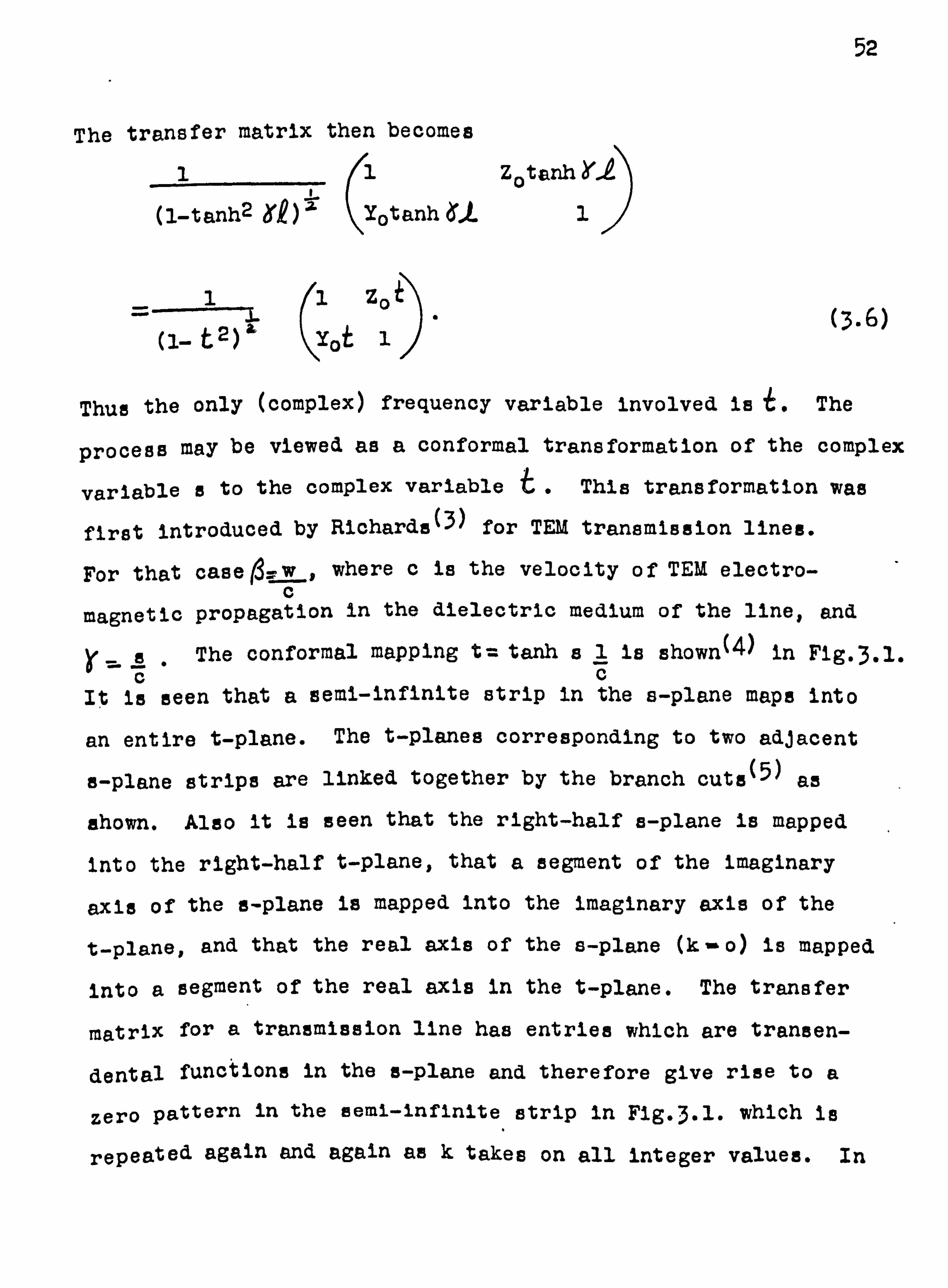
The transfer matrix then becomes
11 Zotanh Y. Q
(1-tanh2 XE)= Yotanh ý, ý 1
C1- t2)&
1 Zoi
Yot 1 (3.6)
Thus the only (complex) frequency variable involved is i. The
process may be viewed as a conformal transformation of the complex
variable e to the complex variable t. This transformation was
first introduced by Richards(3) for TEM transmission lines.
For that case ßr w, where c is the velocity of TEM electro- c
magnetic propagation in the dielectric medium of the line, and
The conformal mapping t= tanh is 1 is shown(4) in Fig. 3.1. cc
It is seen that a semi-infinite strip in the s-plane maps into
an entire t-plane. The t-planes corresponding to two adjacent
s-plane strips are linked together by the branch cute(5) as
shown. Also it is seen that the right-half s-plane is mapped
into the right-half t-plane, that a segment of the imaginary
axis of the a-plane is mapped into the imaginary axis of the
t-plane, and that the real axis of the s-plane (k -o) is mapped
into a segment of the real axis in the t-plane. The transfer
matrix for a transmission line has entries which are transen-
dental functions in the a-plane and therefore give rise to a
zero pattern in the semi-infinite strip in Fig. 3.1. which is
repeated again and again as k takes on all integer values. In

p r
6- (k+ 1/2 Iic 1 u
8 4 gý c O
g h
" (k+ /4ITc 1 branch n O cut 7
branch O
out 3 7O n 3
por s uP A- kT1c 1 u
6 k ba 2
r
O m S
ý. / O
d
cO r 0- 1
(k- /4)TTc 1 c u
unit circle r
p. k
(k- /2)1Tc/1 ,, b u
a
t "Z+ jw C
sl "Q+ So 0
Fig. 3.1. The conformal mapping t" tank al. c
53
the t-plane, however, these entries are (excepting the common
factor (j--L2)10: ) rational functions of 6.
3.3 Driving-Point Impedances and Richards' Theorem.
For most theoretical discussions e may be normalized to
1/c to give
t =tanh a. (3.7)
From the last chapter it is seen that a necessary and suffi-
cient condition for Z(s) to represent the driving-point imped-
ance for a passive network is that Z(s) be positive real, or
that
Re [Z(s)}= 0 when Re [e}0,
and Im [Z(s)]= 0 when Im [s3= 0.
Now it is desired to show that Z(t) for a transmission line
network is a rational real function of t, and furthermore is
p. r.
Suppose a given Z'(t) is a real rational function of t.
Then the driving-point impedance of a basic length of trans-
mission line (commonly referred to as a unit element) of
impedance Zo terminated with Z°(t) is therefore
z(t) A Z' (t)+B
0 z'(t) +D
= Z'(t)+Z t, (3.8) Yot Z'(t)+ i
which again is obviously a real rational function of t.
54
Thus this property cannot be destroyed by adding a unit element.
But the only basic network elements available (other than unit
elements) are open-circuits, short-circuits, and lumped resis-
tors, which are not irrational functions of t (since the net-
work is commensurate), thus by induction all driving-point
impedances are rational functions of t. Also, since all matrix
operations involved in forming the driving-point impedance
consist of addition and multiplication of the real positive
resistances and the real positive coefficients of the trans-
mission line transfer matrix, it follows that any driving-point
impedance Z will be a rational function of t with real positive
coefficients.
Thus
Im ýz(t)J=O when Im [tI =0. (3.9)
It was shown in chapter 2 that a p. r. Z(a) does not have
poles or zeros in the region Re f a}>0. But the poles and zeros
of Z(s) and Z(t) are linked by the mapping shown in Fig. 3. l.
Thies implies that Z(t) (and Z-1(t)) is analytic in the region
Re [t}70. Now since Re ýZ(t)]'_0 when Re [t}=0, by a result
from complex variable theory (Poisson's integral equations)
it is seen that
Re [Z (t)}' 0 when Re {t. ] 0. (3.10)
Egs. (3.9) and (3.10) establish that Z(t) is a positive real
function of t. This same result'can be established through
the mapping shown in Fig. 3.1.

55
A lumped-element network containing no coupled coils
with an impedance function Z(s) may be converted to a trans-
mission line network of impedance Z(t) by replacing the reactive
lumped elements by suitable transmission line stubs. An
inductance of reactance jLw is replaced by a short-circuited
stub of input impedance jztane-/tan &-o; a capacitance of
eusceptance jCw is replaced by an open-circuited stub of input
eueceptance jYtan®°/tan (go, where the factor tan B, has been
Included as a scale factor so that the edge of the pas5band
may be fixed at the arbitrary value of electrical length &p.
As an example, consider the Butterworth insertion lose
function synthesised in section 2.4.2. It is recalled that
PO
_. =1+ vv6 ( 3.11)
PL
The corresponding distributed filter has the insertion lose
function
PO
_1+ tan_ 6&, (3.12)
PL tan6 &o
as shown in Fig-3.2. The lumped element network of Fig. 2.5 is
thus transformed, as shown in Fig. 3.3.
The distributed network of Fig-3-3 consists of a number
of stubs connected to the same physical point in the network
and there is no provision for separation of the stubs for ease

Po
2
1
Fig. 3.2. Butterworth insertion lose function
of Eq. (3.12).
Zi Z1 To
Zo .1Yl Zo =I
8o
6o
Z1tan go -1 Y1tan9 "2
(The stubs are all connected to the same physical point)
Fig. 3.3" A transmission line network having the insertion loss of Fig. 3.2"
ýiý- zero zero zero enlength length
Fig. 3.4. A realizable transmission line network having the insertion lose of Fig. 3.2.
00 2 EE-00 n n+Ao 2n 2n-Q0
Zo -1y. 1 /2 Z- 2 Y- 2 Z- 2 Y- 1 /2 Zo .i
56
of manufacture, and indeed, of physical realizability in the
practical sense. This most important point in the theory of
distributed networks must be emphasized, namely that networks
resulting from any proposed synthesis procedure must satisfy
the elementary condition that it be at least possible to con-
struct them, otherwise the problems are trivial.
The stubs in Fig. 3.3 may be separated by using unit
elements. Any number of unit elements of characteristic im-
pedance 1 and length 4, may be inserted between the last stub
and the load RL = 1, since the terminating impedance of the
network is still 1 (the line is matched), without affecting
the insertion loss. If a means could then be found for
interchanging the position of a unit element and a stub, enough
unit elements could be "dumped" into the network so that each
stub would be separated from its neighbour by a unit element
and the construction of the network is then perfectly feasible.
The resulting network is shown in Fig. 3.4. The method whereby
a simple series or shunt stub may be interchanged in position
with a unit element has been given by Kuroda (6) who presented
a set of identities known as "Kuroda's Identities" which can
readily be used with a simple ladder (shunt C's and series
L's) prototype network. Levy(7) has extended Kuroda's work
to the case where an arbitrary network in t followed by a unit
element may be shown to be equivalent to another (realizable)
network preceeded by a unit element.

57
These procedures have, of course, a sound mathematical
basis expressed most concisely by Richards' theorem(8). This
theorem states that a unit element of characteristic impedance
Z(1) may always be removed from a p. r. Impedance Z(t) leaving
a remainder Z'(t) which is still p. r. Thus for any network
followed by a unit element one computes the driving-point im-
pedance at the port remote from the unit elements and extracts
another unit element of characteristic impedance Z (1) leaving
a p. r. remainder impedance. Using Zo = Z(1) in Eq. (3.8), it is
found that
z(t) z(1) z°(t +-t z(i) (3.13) ZU +. t It
where a unit element of characteristic impedance Z(l) is
extracted from Z(t) leaving a remainder Z'(t). Solving for
Z'(t),
Z'(t)= Z(l) ZZ(t)-
t z(i (3.14)
and Richards' theorem states that ZI(t) is positive real if
Z(t) is p. r. It is evident from Eq. (3.14) that Z'(t) has a
factor (1-t) in numerator and denominator. After cancellation
of this factor the degree of Z'(t) will be equal to the degree
of z(t). If, however, Z(-1)ä -Z(1) then the factor (1+ t)
also exists in the numerator and denominator of Z'(t), and
hence it will be of lower degree than z(t).
In order to apply Richards' theorem when it is desired
to extract a unit element from a transfer matrix, the follow-
58
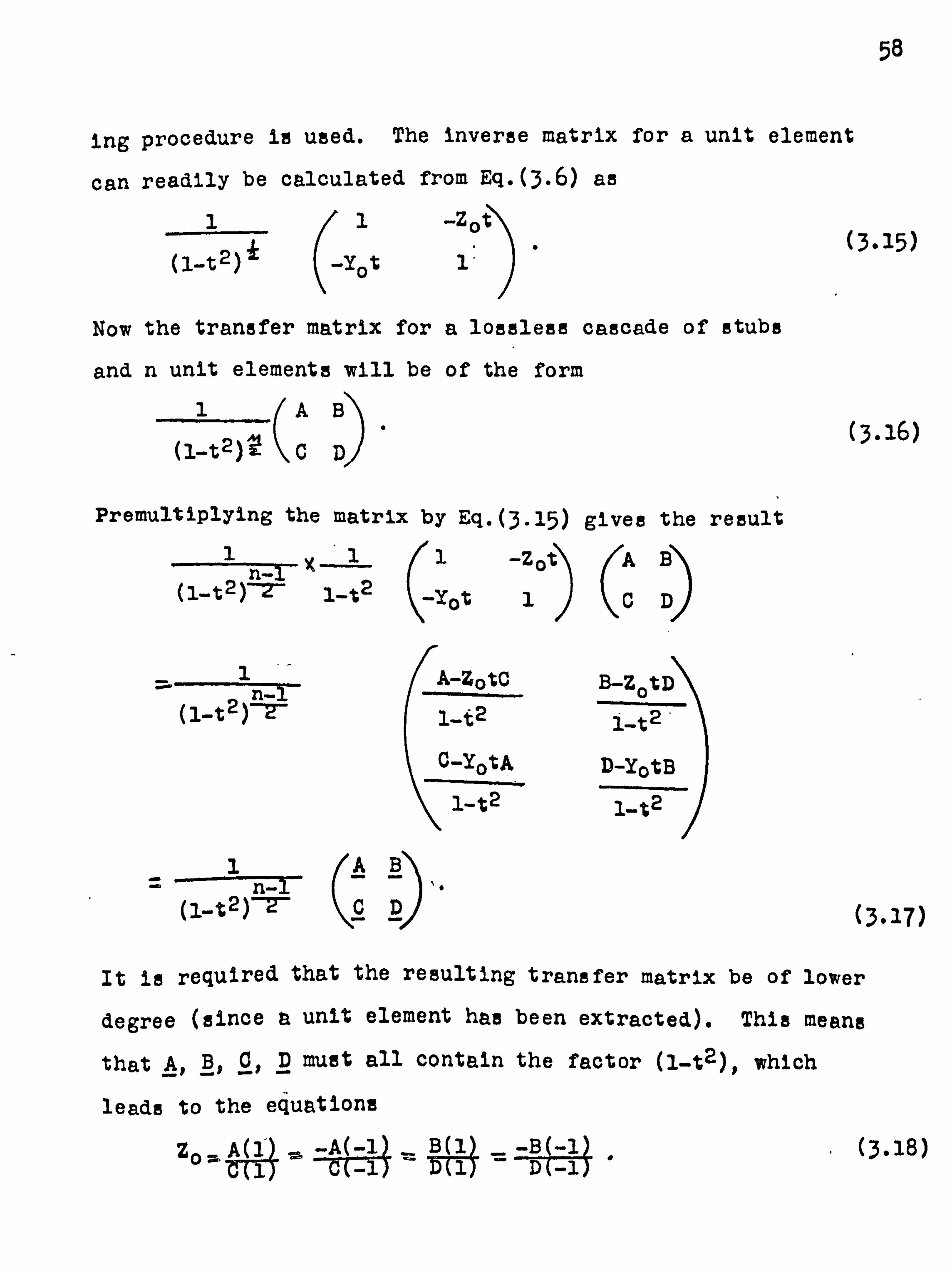
Ing procedure is used. The inverse matrix for a unit element
can readily be calculated from Eq. (3.6) as
-Z of (3.15) tl-t2)ß Yot 1
Now the transfer matrix for a 1ossless cascade of stubs
and n unit elements will be of the form
1A8 " (3.16)
(1-t2) aCD
Premultiplying the matrix by Eq. (3.15) gives the result
1nX11 -Z of AB - (1-t2)ß 1-t2 -Yot 1CD
A-ZotC B-ZotD (1-t2)ß 1-t2 1-t2
C-YotA D-YotB
1-t2 1-t2
1AB ---' n_i (1-t2)`ß C (3.17)
It is required that the resulting transfer matrix be of lower
degree (since a unit element has been extracted). This means
that A, B, Q, D must all contain the factor (i-t2), which
leads to the equation!
Zo m A(1 m -A(-11, = B(1
= -B(_i
59
It only rem. ins_to show that the reduced degree matrix (3.17) represents a realizable transmission line network.
Now Richards' theorem states that from the driving-point
impedances A/C and B/D (corresponding to the output open-and
short-circuited), an impedance equal to A(1 )/C(1) and B(1)/D(1)
may be extracted, respectively, with the result that A/C and
B/D are positive real driving-point impedances. But this
impedance value is precisely that given by Eq. (3.18), and so
the desired unit element extraction may be carried out.
The proof of Richards' theorem is simple and interesting.
The voltage reflection coefficient between Z(t) and a real
impedance Z(1) is, by Eq. (2.17),
r_ z(t - z(i , Z(' t) i and it is easily derived that the reflection coefficient between Z'(t) and Z(1) is
rýct)=rcO i-t Now since Z(t) is p. r., P (t) Is bounded real (b. r. ) and
1 P(jW) P(-jW)>_o, where t --=f+jW.
But
r 1(1w) r' (-jw) = r(iw) r(-iw). Therefore ("(t) is b. r. provided I' (t) has a first order
zero at t =1, which, since Z(1) is the impedance of the ex-
(2.17)
tracted unit element, it has. Hence the associated Z'(t) is p. r.

60
The application of this theorem is straightforward. In
simple ladder design a specified Z(t) is realizable with series
short-circuited and shunt open-circuited stubs. Now by applica-
tion of Richards' theorem after extraction of each stub the
stubs may be separated by unit elements and a physically
realizable design completed. If the transfer matrix approach
is used, the starting point is to determine the transfer matrix
for the lossless network (which is connected between the source
and load resistances R. and RL) from the reflection coeffic-
ient. This matrix is then premultiplied and/or postmultiplied
by the transfer matrix of a unit element with characteristic
impedance R5(for premultiplication) or RL(for postmultiplication)
until n lines are in place, n being the number of unit elements
required to separate the stubs. The decomposition of the
augmented transfer matrix then proceeds in the customary manner.
This approach is computationally longer than the preceeding
method, but offers accuracy checks at each stage.
Both of these methods and that of "jumping" unit elements
into the prototype network have advantages. The methods using
Richards' theorem are beat where explicit formulae for the
element values are not available, and the network must be
synthesized directly anyhow, whereas, if explicit formulae
are available for the prototype (as with Chebyghev or maximally
flat filtera(9)), the alternative method may be most conven-
tent. A drawback to using unit elements as "spacers" between
61
stubs, however, is that they do not contribute to the insertion
loss specification. In fact, in the above design methods the
only effect of the unit elements is to give added delay between
input and output. It is possible to incorporate these unit
elements into the insertion-lose specification(10), which will
result in superior performance for the same number of network
elements.
The Darlington insertion loss method outlined in the
last chapter may now be employed in the synthesis of tranemie-
eton line networks. From a given structure the form of the
insertion loss (as a function of t) may be deduced by analysis.
The approximation problem then consists of arranging the co-
efficients in the insertion lose to meet some specification
function as closely as possible, within the limitations imposed
by the form of the insertion loss. From the insertion lose
the voltage reflection coefficient is calculated (by factoriza-
tion), and the transfer matrix for the loaelese transmission
line network is established. Next the transfer matrix may be
augmented, if necessary, to provide enough unit elements for
physical realizability, as discussed previously. Unit elements (and stubs) are then removed by multiplying the overall
transfer matrix by the inverse matrix of the desired network
element with the requirement that the resulting transfer
matrix be of lower degree.
62
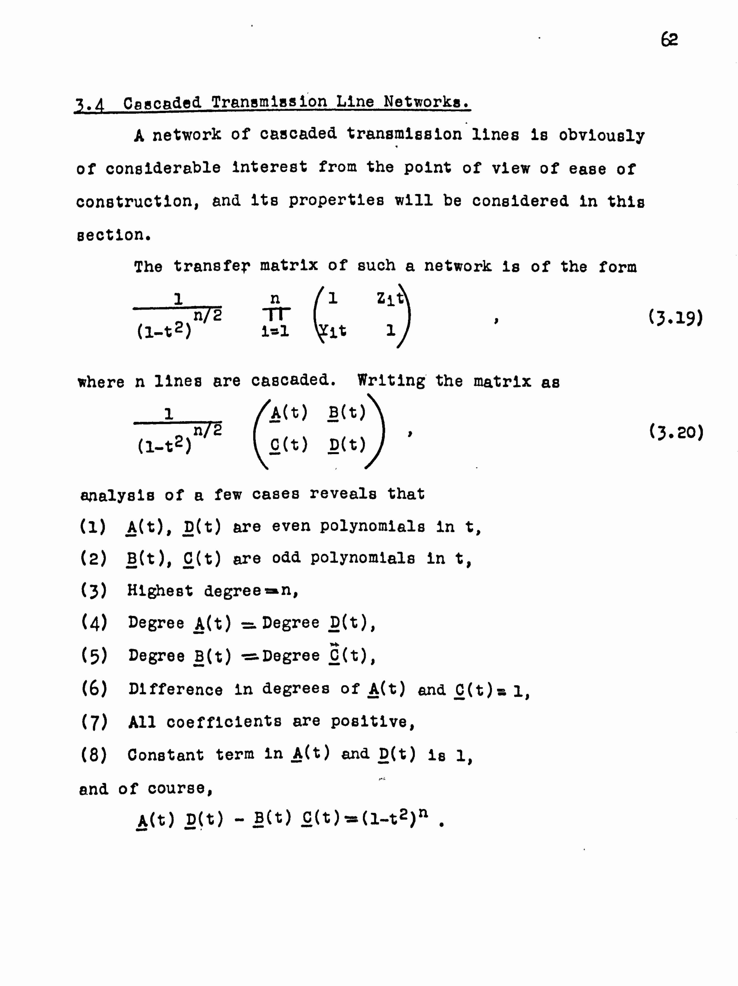
3.4 Cascaded Transmission Line Networks.
A network of cascaded transmission lines is obviously
of considerable interest from the point of view of ease of
construction, and its properties will be considered in this
section.
The transfer matrix of such a network is of the form
1n Zit n/2 T'ý , (1-t2) i=1 it 1
where n lines are cascaded. Writing the matrix as
1 7A(t) B(t)
(i-t2)n 2
0(t) D(t) ,
analysis of a few cases reveals that
(1) A(t), D(t) are even polynomials in t,
(2) B(t), C(t) are odd polynomials in t,
(3) Highest degreesn,
(4) Degree A(t) . Degree D(t),
W* (5) Degree B(t)-=Degree C(t),
(6) Difference in degrees of A(t) and C(t)_ 1,
(7) All coefficients are positive,
($) Constant term in A(t) and D(t) is 1,
and of course,
(3.19)
(3.20)
A(t) D(t) - B(t) C(t) =(1-t2)n .
63
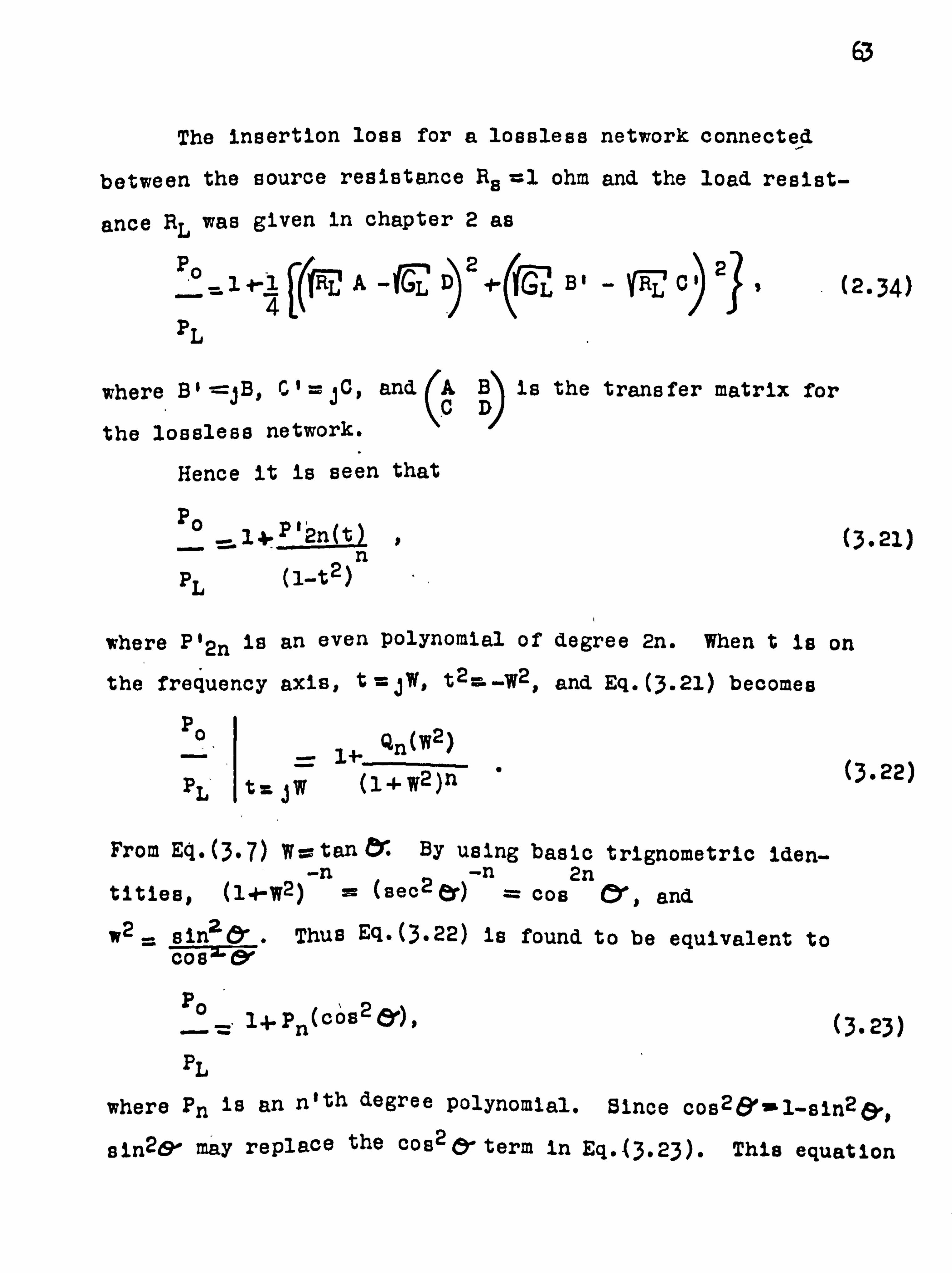
The insertion loss for a lossless network connected
between the source resistance R. =1 ohm and the load resist-
ance RL was given in chapter 2 as
02 A-)2(y' B' -ycý ,
PL
where B' =jB, C' = jC, and CA
the loasless network.
Hence it is seen that
PO
n PL (1-t2)
(2.34)
(3.21)
where P'2n is an even polynomial of degree 2n. When t is on
the frequency axis, t cjW, t2 = -W2, and Eq. (3.21) becomes
PO Qn(W2)
-=1 " (3.22) pL t: JW (14. W2)n
From Eq. (3.7) W- tan 8X By using basic trignometric iden-
tities, (1+-w2)-n = (sect ©r) -n = cos
2n O', and
W2 _ sing O'. Thus Eq. (3.22) is found to be equivalent to Cos'
Po = 1+pn(cos26r), (3.23)
PL
where Fn Is an n'th degree polynomial. Since coat e'= 1-sing &,
singe' may replace the cost e- term in Eq. (3.23). This equation
B is the transfer matrix for D
64
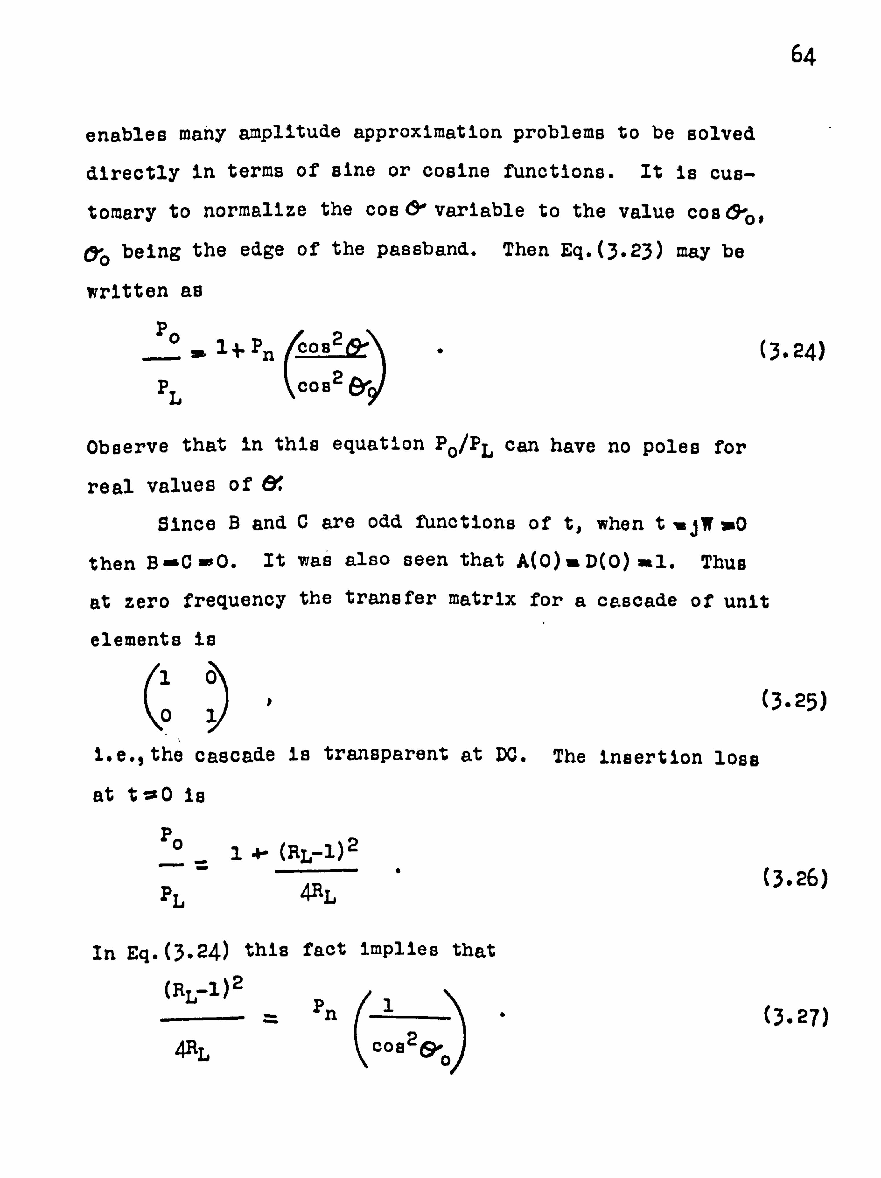
enables many amplitude approximation problems to be solved
directly in terms of sine or cosine functions. It is cus-
tomary to normalize the cos 6' variable to the value cos &0,
&o being the edge of the passband. Then Eq. (3.23) may be
written as
20 P°
1+ Pn 2 (3.24)
pL ýCOS2
e-
Observe that in this equation Po/PL can have no poles for
real values of &
Since B and C are odd functions of t, when t ajW a0
then B -&C moo. It was also seen that A(0) s D(0) : l. Thus
at zero frequency the transfer matrix for a cascade of unit
elements is
10
01
i. e., the cascade is transparent at DC.
at t%cO Is
-1+ (RL-1)2
PL 4RL
In Eq. (3.24) this fact implies that
(RL_1)2 Pn l
L0082&,
The insertion lose
(3.25)
(3.26)
(3.27)
65
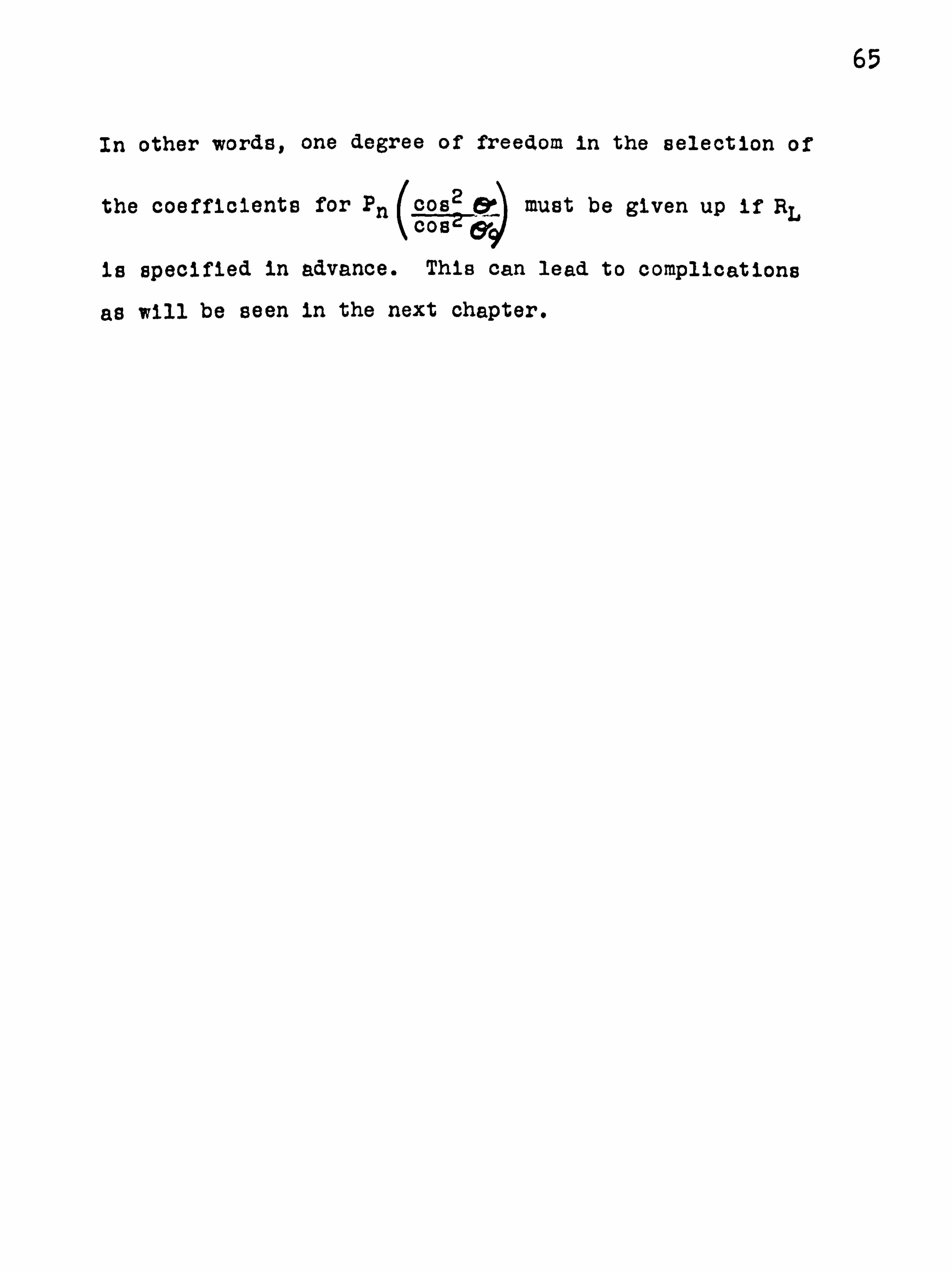
In other words, one degree of freedom in the selection of
the coefficients for Pn (.
2-0-8.2 co
ý_ must be given up if RL
is specified in advance. This can lead to complications
as will be seen in the next chapter.

66
Chapter 3 REFERENCES
1. Ragan, a. L.: "Microwave Transmission Circuits".
(Radiation Laboratory Series, McGraw-Hill, 1948).
2. Protonotarios, E. N. and Wing, 0.: "Analysis and intrinsic
properties of the general nonuniform transmission
line", IEEE Trans., 1956, MTT-15 , pp. 142-150.
3. Richards, P. I.: "Resistor-transmission-line circuits",
Proc. I. R. E., 1948, }A, p. 217.
4. Kober, H.: "Dictionary of Conformal Representations".
(Dover Publications, 1947), p. 88.
5. Quillemin, E. A.: "The Mathematics of Circuit Analysis".
(M. I. T. Press, 1949), PP"310-317.
6. Ozaki, H. and Ishii, J.: "Synthesis of a class of strip-
line filters", IRE Trans., 1958, CT5, p. 172.
7. Levy, R.: "A general equivalent circuit transformation
for distributed networks", IEEE Trans, 1956, C_T12,
P-457. 8. Richards, P. I.: "General impedance-function theory",
Quart. Math., 1948,6, p. 21.
9. Weinberg, L.: "Network Analysis and Synthesis".
(McGraw-Hill, Inc., 1962), pp. 651-669.
10. Carlin, H. J. and Kohler, W.: "Direct synthesis of bend-
pass transmission line structures", IEEE Trans.,
1965, MTT-1 , pp. 283-297.
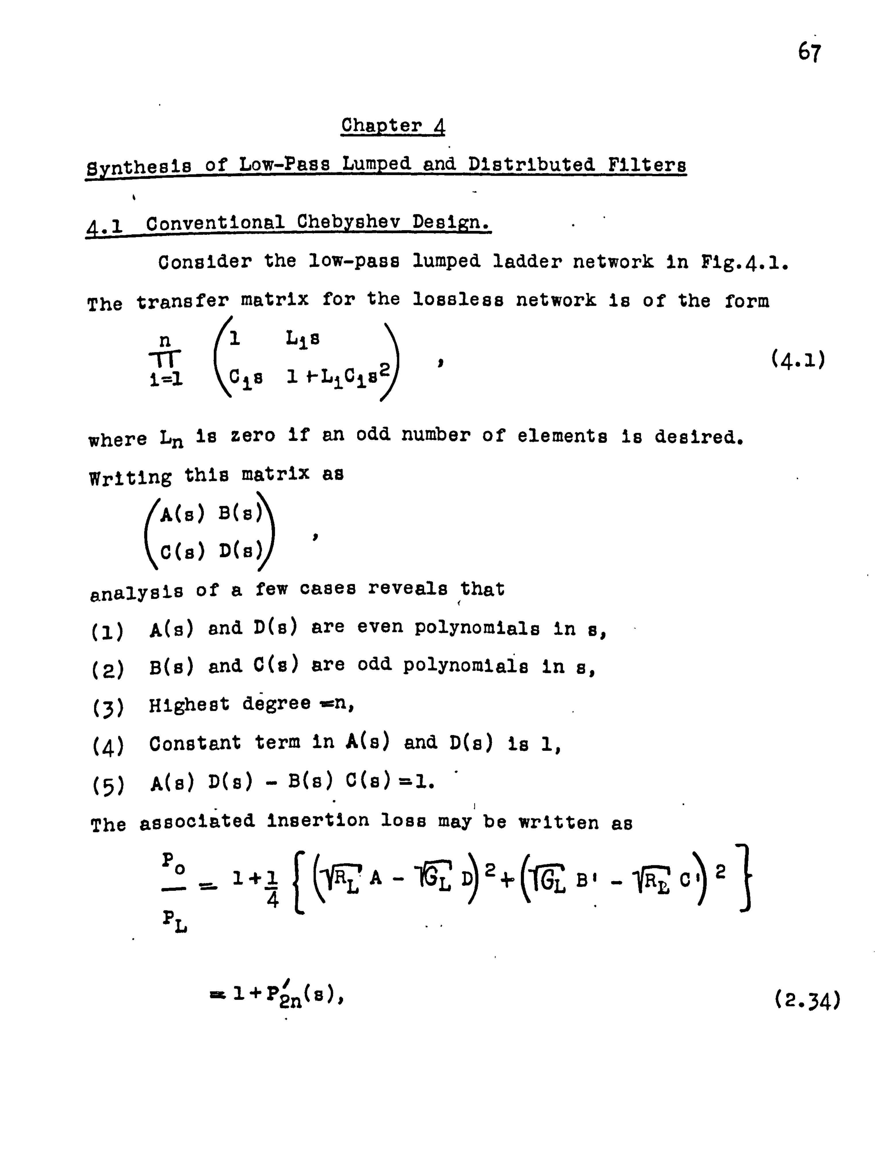
67
Chapter 4
Synthesis of Low-Pass Lumped and Distributed Filters
4.1 Conventional Chebyshev Design.
Consider the low-pass lumped ladder network in Fig. 4.1.
The transfer matrix for the losslesa network is of the form
n1 Lis
i=1 Cis 1 t-LjCis2
where Ln is zero if an odd number of elements is desired.
Writing this matrix as
A(s) B(s)
C(s) D(s)
analysis of a few cases reveals that
(1) A(s) and D(s) are even polynomials in s,
(2) B(s) and C(s) are odd polynomials in s,
(3) Highest degree =n,
(4) Constant term in A(s) and D(s) is 1,
(5) A(s) D(s) - B(s) C(s) =1.
The associated insertion loss may be written as
2 P° _ 1+1 "ýRLA-D 2# (
GL B'[R-- C2
PL
1+PPn(8), (2.34)

R8.1 L1 L2 Ln
T C1 TC2 On RI.
Fig. 4.1. Low-pass lumped ladder network.
PO
d
X
Fig. 4.2. Ideal low-pass'insertion loss specification function.

68
, w, where P2n is an even polynomial of degree 2n. When so
P° _1 +Pn (w2),
P L
where Pn is a polynomial of degree n. Now the form of the
insertion loss is just the same for this case as for the cas-
cade of transmission lines in the last chapter, i. e.,
PO _
14-Fn (x2) ,
PL
(4.2)
where xsw for the lumped case and x= cos or sin for the cos sinob
distributed case.
An ideal low-pass filter with RS -R L2-1 would have the
insertion loss shown in Fig. 4.2, where the passband has been
normalized to unity. Since no finite-degree polynomial can
represent this "brick wall" response exactly, which polynom-
lal of degree n will approximate it best? The problem of
determining such an optimum polynomial can be more precisely
stated as follows:
Among all polynomials of degree not exceeding n and
not exceeding unity in absolute value over the interval
_] X`1, determine the polynomial that exceeds all others
outside this interval. The answer to this question turns out
to be Tn(x), which is a Chebyshev polynomial of the first
kind(').
Tn(x) may be defined by
Tn(x) = cos(ncos-lx). (4.3)

69
As x goes from -1 to 1, cos-goes from Tito 0 radians
(principal value) and so ncos-lx goes from nW'r to 0 radians.
This means that Tn(x) oscillates between -1 and 1n times
as x goes from -1 to 1. If 1X( 1, then cos-1(x) _j cosh-1(x),
and Tn(x). cosh(n cosh-lx). That Tn(x) is a polynomial in
x may be shown as follows.
Let y= cos-l(x). Then, by use of trignometric identities,
Tn-ý, l(x). bcos(n++1)y-cos ny cos y- sin ny sin y
-cos ny cos Y+. 1 cos(n+l)y -1 cos(n-l)y, 22
which gives
Tn+1(x)" . cos(n+1)y m2coa ny cos y- cos (n-1)y.
NoW cog Y=x. Therefore,
Tnt-I (x) = 2xTn(x) - Tn-1(x)" (4.4)
Though Chebyshev polynomials are used only for n >O, the
definition also holds for n=0. Thus by inspection it is
seen that To(x) =1 and T1(x)=x. Eq. (4.4) shows by induction
that Tn(x) is indeed a polynomial. T2, T3, and T4 may next
be computed from To and T1 and from the recurrence relation
Eq. (4.4) as
Tl(x)- x,
T2(x) = 2x2 -1, T3(x) =#3 -3x..
T4(x) =8x4-8x a+ 1. (4.5)
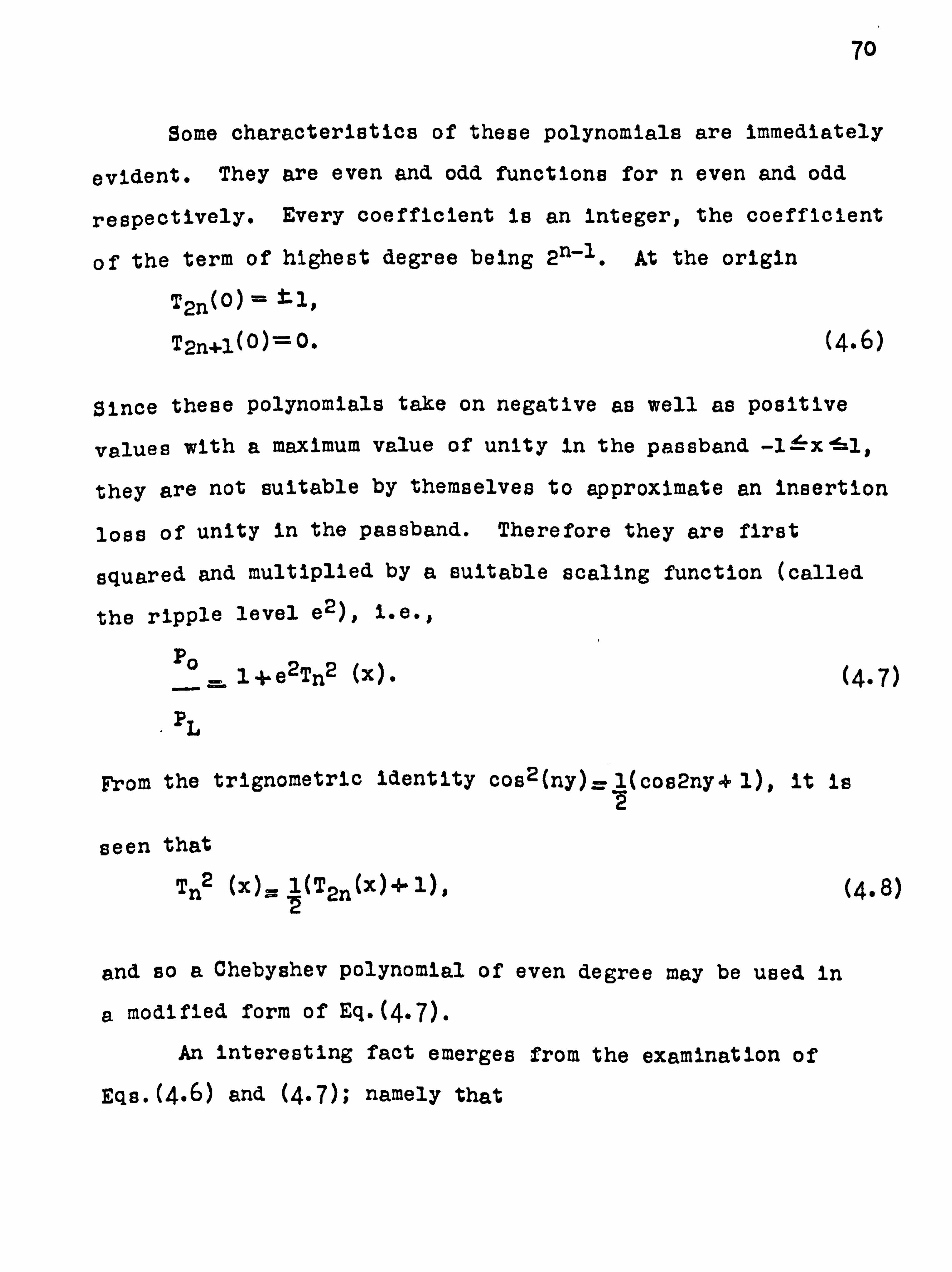
70
Some characteristics of these polynomials are immediately
evident. They are even and odd functions for n even and odd
respectively. Every coefficient is an integer, the coefficient
of the term of highest degree being 2n-1. At the origin
T2n(0) = tl,
Ten+1(0)=0. (4.6)
Since these polynomials take on negative as well as positive
values with a maximum value of unity in the passband -1 ýx mal,
they are not suitable by themselves to approximate an insertion
loss of unity in the passband. Therefore they are first
squared and multiplied by a suitable scaling function (called
the ripple level e2), i. e.,
PO ®1+e2Tn2
(X).
PL
(4.7)
From the trignometric identity cos2(ny)_ 1(coa2ny 4 1), it is 2
seen that
Tn2 (x)= 1(T2n(x)+ 1), (4.8)
and so a Chebyshev polynomial of even degree may be used in
a modified form of Eq. (4.7).
An interesting fact emerges from the examination of
Egs. (4.6) and (4.7); namely that

71
PO
PL xd0
n odd,
1-ß-e2 n even.
(4.9)
In chapter 3 it was found that
P° gl + (R-1 2,
PL X-0 4R
where x =sin O/sin ®o and Rz RL/Rs. The same is seen to be
true for the structure in Fig. 4.1, (where now x . --w), since
the loasleas network is completely transparent at DC.
(4.10)
Comparison of Egs. (4.9) and (4.10) reveals that, for the
Insertion loss specification (4.7), R is also determined, i. e.
Ra1 for n odd,
(R-1)2 ® e2 for n even.
This specification has been used by Levy(2) in the design of
distributed low-pass filter prototypes (where x: sin O/sin C. ).
A distributed filter is defined as a doubly terminated cascade
of commensurate length transmission lines, as discussed in
chapter 3.
The insertion loss specification (4.7) may be general-
ized to accommodate an arbitrary load to source resistance
ratio with the addition of another parameter, e. g.
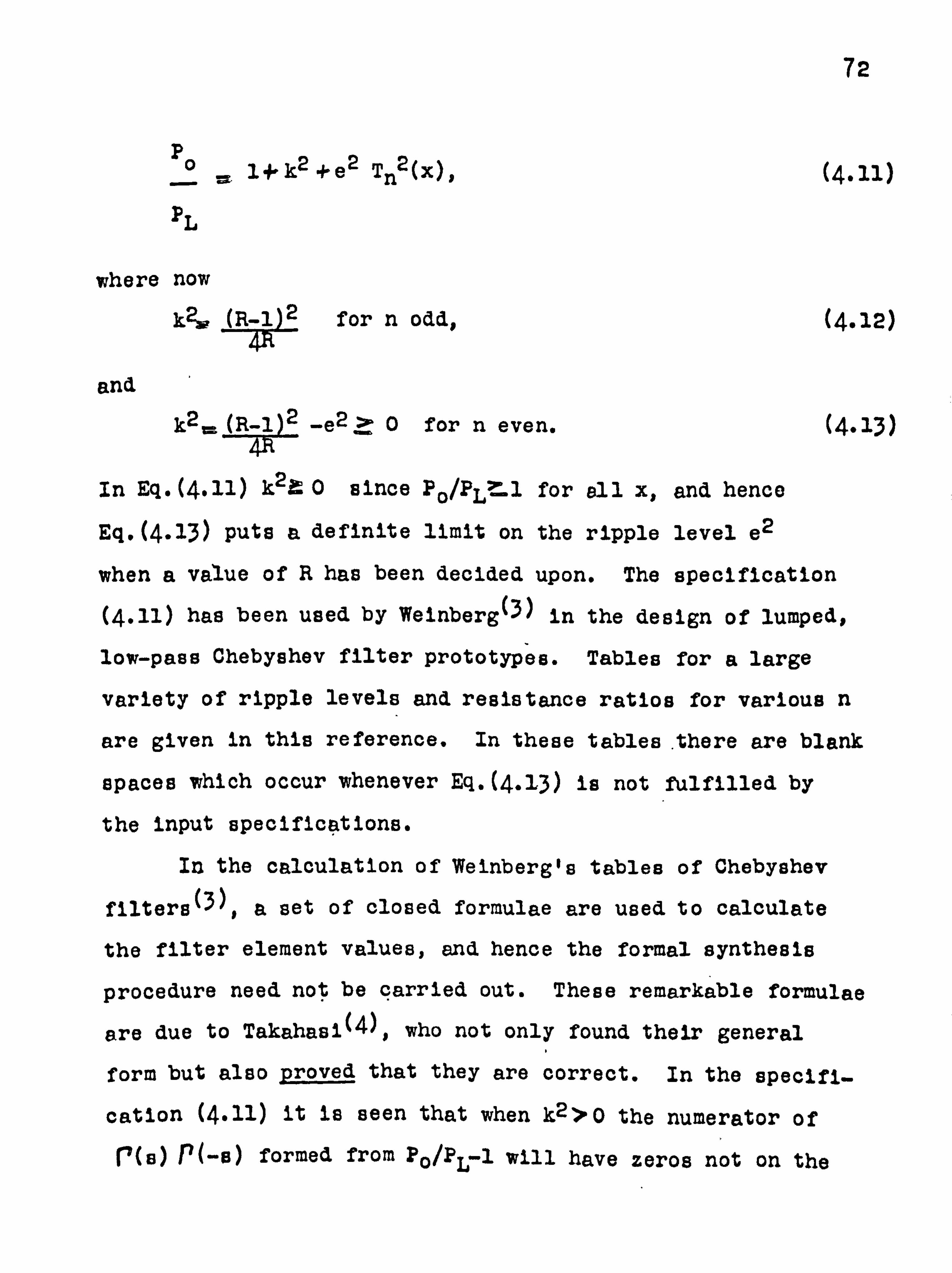
72
P°
,ä 14 k2 + e2 Tn2(x), (4.11)
PL
where now
k2w (R-1)2 for n odd, (4.12)
and
k2= (R-1 2 -e2 0 for n even. (4.13)
In Eq. (4.11) k2& 0 since Po/PL> 1 for all x, and hence
Eq. (4.13) puts a definite limit on the ripple level e2
when a value of R has been decided upon. The specification
(4.11) has been used by Weinberg(3) in the design of lumped,
low-pass Chebyshev filter prototypes. Tables for a large
variety of ripple levels and resistance ratios for various n
are given in this reference. In these tables. there are blank
spaces which occur whenever Eq. (4.13) is not fulfilled by
the input specifications.
In the calculation of Weinberg's tables of Chebyshev
filters(3), a set of closed formulae are used to calculate
the filter element values, and hence the formal synthesis
procedure need not be carried out. These remarkable formulae
are due to Takahasi(4), who not only found their general
form but also prove d that they are correct. In the epecifi-
cation (4.11) It is seen that when k2>0 the numerator of r(e) r(-s) formed from Po/pL 1 will have zeros not on the
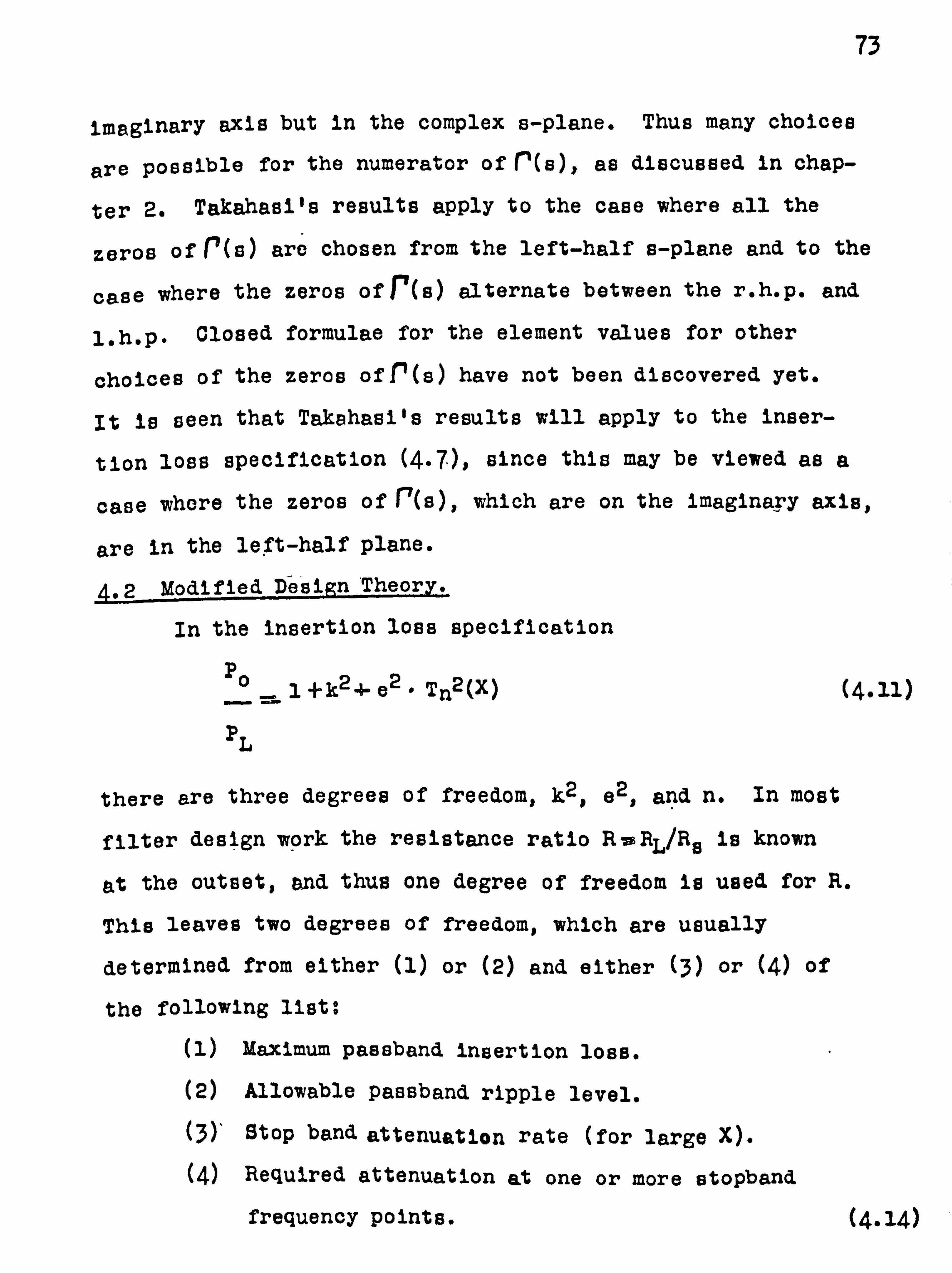
73
imaginary axis but in the complex s-plane. Thus many choices
are possible for the numerator of r(s), as discussed in chap-
ter 2. Takahasi's results apply to the case where all the
zeros of r°(s) are chosen from the left-half s-plane and to the
case where the zeros of r(s) alternate between the r. h. p. and
l. h. p" Closed formulae for the element values for other
choices of the zeros off(s) have not been discovered yet.
It is seen that Takahasi's results will apply to the inser-
tion loss specification (4.7), since this may be viewed as a
case where the zeros of r7(s), which are on the imaginary axis,
are in the left-half plane.
4.2 Modified Design'Theory.
In the insertion loss specification
PO
m1 +k2#- e2 " Tn2(X) (4.11)
PL
there are three degrees of freedom, k2, e2, and n. In most
filter design work the resistance ratio R: RL/Rs is known
at the outset, and thus one degree of freedom is used for R.
This leaves two degrees of freedom, which are usually
determined from either (1) or (2) and either (3) or (4) of
the following list:
(1) Maximum passband insertion loss.
(2) Allowable paseband ripple level.
(3)' Stop band attenuation rate (for large X).
(4) Required attenuation at one or more stopband
frequency points. (4.14)

74
In the design of a microwave distributed filter the
input and output resistances are nearly always equal to the
system characteristic impedance (which is usually 50-t-2). In
this case R1. In lumped filter design a doubly terminated
filter having a R- 1 (which gives maximum power transfer when Po
1) is also frequently met in practice. Thus the R-1
case is by far the most important one in low-pass filter design.
When R=1, it is seen that, for n odd, k2 a0 (from Eq. (4.12))
and so
Po 1 +e 2 Tn2(X) " (4.7)
PL
Since Tn(X) is an optimum polynomial, as seen earlier, this
specification is an optimum one for n odd. For n even,
Eq. (4.13) states that
k2 (R-1)2 -e2 Z 0, (4.13)
which implies that k2=e2 ®0 and leaves Eq. (4.11) in the P
form ® 1, which is clearly a non-optimum filter specifi- L
cation:. This is confirmed in Weinberg's tables(3), where
there are blank spaces for n even and R vat in the Chebyshev
designs. Since approximately half of all filter design
problems should lead to a structure with an even number of
sections, it is clear that half of the existing Chebyshev

75
low-pass filter designs (for R -wl) have one more section than
is necessary. From a cost standpoint this fact is far from
trivial; reducing a five section filter to a four section one
represents a 20% saving.
When n is even it appears that a rearrangement of the
three degrees of freedom in the specification Eq. (4.11) is
desirable. In particular, a Chebyshev-like polynomial is
desired which is equiripple in the passband except at the
origin, where it assumes the correct level for the specified
value of R.
The even degree Chebyshev polynomial will now be examined
in greater detail. From Eq. (4.3), T2n(X) is defined as
T2n(X) = cos(2n cos-1 X)
cos (ncos-1(2X2-1)) _ms cos (2-,, (4.15)
since cos'"1(2X2-1)' 2cos-1 X (or 2X2-1----cos 2 cos-1 X=Tl(X)).
Inspection of this equation is interesting. At X t1, (2X2-1)= 1,
co e-1(1) = 0, and so (& 0. At X=00 (2X2-i)-i, cos-1(-1)' 1T,
and so to -- nöi . It is now desired to modify Eq. (4.15), so
that dgl-w 0, but n 1T - : ý% IC- nit . Then cos 0 would go from
1 (at X- ±1 ), ripple between +1 and -1 in the passband, and
finish at a predetermined DC level at X=0. Eq. (4.15) may
gain two degrees of freedom by letting
L2n(X, a, b)= cos(n cos-1 (ax2 - b)). (4.16)
At xs ±1, Q#1ý 0, which implies that a-b mal, or, that a_1 +b.

76
Thus Eq. (4.16) loses one degree of freedom and becomes
L2n(X, b)- cos(n cos-1 ([ 14bJX2 -b)). (4.17)
Notice that ((El 4. b] ) X2 -b) goes from 1 to -b as X goes from
t :i to 0. Assume dbl' 1. Then I L2n, 1 for, Xj` 1. If this
were not true, then cos-l( E1 *b] X2 -b) would become imaginary,
and L2n is no longer equiripple when IX16 1. In fact, the
relationship between the DC level and b may easily be shown to
be
(9La sin-1 ILDOI
, (4.18)
and that
b v--cos 'rT-2 tel. (4.19) n
In the special case of the even n, Rz 1 low-pass filter design,
LDC 0,9
lL- 0, b -, cos , and
L2n(X, b) = cos (ncos-l( [ .. cos X2 - cos .
ý) 2n 2n
= Tn 1+ cos .j X2 - cos (4.20)
2n 2n
These last four equations have been reported by Lind(5),
with Eq. (4.20) then being used for the design of lumped and
distributed low-pass. filters. Egs. (4.17), (4.18), and (4.19)
have also been found by Jonea(6), (7), although no specific
mention was made of applying them to even n, equally termina-
ted filter designs. Eq. (4.20) has been reported by Vasil'yev(8),

77
who obtained this equation through a differential equation
solution. He also proved that this function is optimal (for the
Ra 1, even n case) and then he used it in computing a. table of
lumped element low-pass, filter prototypes with from two to ten
sections. Vasil'yev does not apply the result to the synthesis
of distributed filters, however, and he does not state the
extension in Egs. (4.17), (4.18), and (4.19).
In Fqs. (4.18) and (4.19), let JLDCJ: -l (which should
, result in the conventional Chebyshev design). Then &L=-T.
b- 1, and Eq. (4.17) becomes
L2n(X, 1) = cos(n cos 1(2X2-1)),
which checks with Eq. (4.15). As the value of b is decreased
from unity, it can be shown that the zeros of L2n(X, b) shift
towards the origin, and the attenuation rate of L2n in the
stopband is decreased. When b reaches the lower limit of
cos '%, the two zeros of L2n closest to the origin coalesce zn
at the origin. Ln is equiripple in the paasband(except at
the origin) during this entire process, of course.
It is interesting to compare the stopband performance
of Ln(x, CosTf) (n even) to that of Tn(X), the optimum n
polynomial. In Fig. 4.3 is shown the etopband attenuation
curves for a number of M (from 2 to 12) section low-pass
filter designs. The Passband ripple level in each case is
.5 dB. The broken lines represent optimum Chebyshev designs,

Attenuation (dB)
tap 4"ý `, 12 /1}0 // 9i8ri
eo
60 ' r' / ,rf r .I r
4 40 ;::
'I / ý
20
090.8 0.7 0.6 0.5 0,4 o., ;t
Fig. 4.3.8topband performance of G)4 (---) and rM (- -) for various M, each having a .ý dB pa.. band ripple . evsi.

78
which means that for M even, Rt1. The solid lines represent
the results obtained through the specification
Po 1+ e2 LM2(X).
PL
where M is even and R= 1.
(4.21)
It can be seen from these curves that Eq. (4.21) yields
filters having a atopband attenuation only slightly inferior
to those of the corresponding Chebyshev filters. For a given
wl 71 the difference between the attenuation levels of the
filter types compared vanishes asymtotically with increasing
n. A proof that LM is the optimum polynomial (for ä given DC
level) is given at the end of this chapter.
40 ynthesis of Even N9 Equally Terminated, Low-Pass Filters.
d. ß. 1. Lumped element filtere.
The specification function used in this design is
Po .1 +-e 2 L2n (w, co$ lT
2n PL
_ L+e2 Tn2 [1 +-cos ] w2 - cos Tr' , (4.21)
2n 2n
where w is the standard lumped frequency variable. In the
Darlington procedure the next 'step is to find the poles and
zeros of r(s).
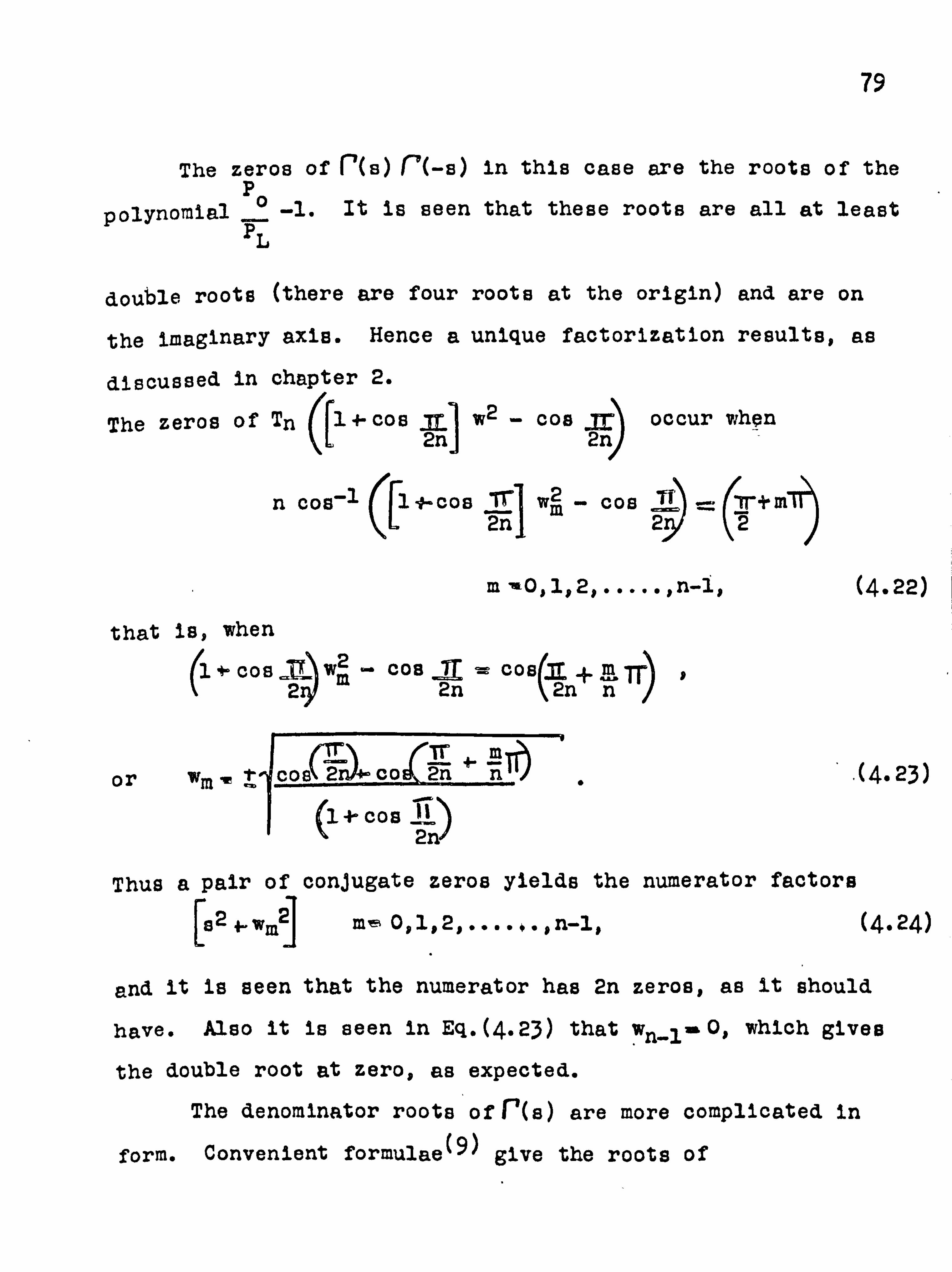
79
The zeros of r(s) ('(-s) in this case are the roots of the P
polynomial Po -1. It is seen that these roots are all at least L
double roots (there are four roots at the origin) and are on
the imaginary axis. Hence a unique factorization results, as
discussed in chapter 2.
The zeros of Tn [1+-cos IL w2 - cos g occur when 2n] 2n
n cos-1 ([i
COs 2n w2 - cos
(rri. ucr
22
(4.22)
that is, when
CZ ý° COS )WM2 cos
,l C08 ý. J1
2 2n C2n
n fi
+. jR or wm t coa'ý 2aß° co&2n ný (4.23)
OS t) (1c 2n®
Thus a pair of conjugate zeros yields the numerator factors
[2+. w2] m' 0,1,2,....,., n-1, (4.24)
and it is seen that the numerator has 2n zeros, as it should
have. Also it is seen in Eq. (4.23) that wn_1. "0, which gives
the double root at zero, as expected.
The denominator roots of r'(s) are more complicated in
form. Convenient formulae(9) give the roots of

80
as
1 *-e2 Tn2(Z)-O,
Zm-am * jbm, --sieh O2
sin (2m -. 1 Tr+ j cosh r2 cos 2m4t T1 2n 2n
m , le 0,1,2 , .... 2n-1,
where c42' Isinh 1(�
e. n
From Eq. (4.21),
or
.= am+jbm, -(1 + cos ? rlsm - (cos 2 2nl
sm -cos IT -a -j bm l, 1,2 `+ 2n m,
1} coa J'[ 2n
which gives rise'to two roots in the s-plane that are 1800
apart and equidistant from the origin. Now in Eq. (4.25)
there will also be a root of the form Zm' am - , bm, which
gives rise to two roots in the s-plane which are conjugate
to the Zm roots. The four roots from Zm and Zmo in the s-
plane thus form a quartet of roots which are symmetrical
(4.25)
(4.26)
(4.27)
with respect to the real and Imaginary axes. The two l. h. p.
roots are then selected for the denominator of r(s)" Alto-
gether it Is seen that the denominator will have 2n roots.
Now (s) may be written as 2n
r(s) Kil (s-8j)
2n "Cr ýs-sk) ký3
(4.28)

81
K is determined from the fact that as s --, w *o°, the Inser-
tion loss becomes infinite, and so This
implies that K ea1 in Eq. (4.28), and so
2n r(s)='-' (s-ai)
i1 (4.29) 2n
ka1
In chapter 2 it was found that
P(s)- (A-D (B-c (4.30)
where (C B) Is the transfer matrix for the lossless network
connected between the Rs $ RL a1 loads. It has also been
established that for the network in Fig. 4.1, B and C are odd
polynomials in s, A and D are even polynomials, and the
constant term in A and D is 1. Comparing Egs. (4.29) and (4.30),
therefore, BmC, and the structure is antimetrical. This (10)
means that
Ln- i --- C1r1,
On-i = Ll ýi
(4.31)
in Fig-4-1. Thus the synthesis need only be carried out for
half the network, and Eq. (4.31) then gives the remaining
element values. So that both A and D have a constant term
of unity, both numerator and denominator of Eq. (4.30) are
multiplied by a factor which leaves the denominator constant
term equal to 2.

82
B matrix by The last step is to decompose the (A CD
successive premultiplication by the inverse matrix of the
desired element in Fig. 4.1, with the requirement that the
overall matrix be of lower degree. Recall in chapter two this
leads to two independent equations for the element value.
Let the two values so found be Z and Z'. If no numerical
errors occur in the synthesis process, then Z -Z'. In the
computer program that was written for the synthesis procedure,
however, it was found that serious rounding errors did occur.
When first written, the computer program calculated Z
from the A and C polynomials, and then the value was used to
reduce the degree of A and C. Similarly, Z' was calculated
from B and D. and was then used to reduce the degree of B and
D. Next, the computer program printed out the first n digits
in Z and Z' that agreed, up to five digits. The computer
itself was an English Electric KDF-9 computer, with 11 digit.
accuracy. It was found that roughly a digit of accuracy was
lost for every section in the filter. Since up to 20 element
designs were desired, the above method of obtaining element
values was not adequate. A slight modification in the pro-
gram improved the accuracy. This was to reduce the degree of
the A and C. and B and D polynomials, not by using Z and Z',
but by using
Zla k(Z) -ie'(1-k)Z',
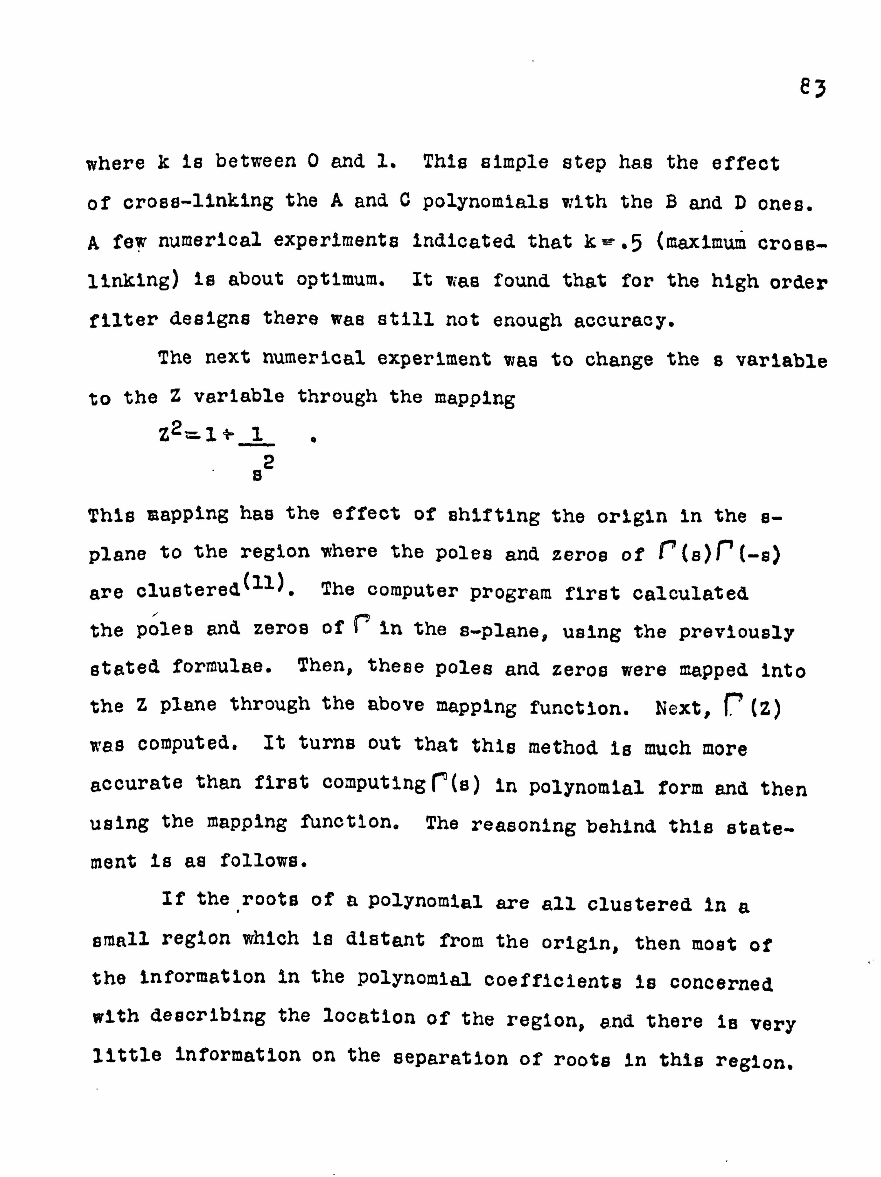
83
where k is between 0 and 1. This simple step has the effect
of cross-linking the A and C polynomials with the B and D ones.
A few numerical experiments indicated that k c. 5 (maximum cross-
linking) is about optimum. It was found that for the high order
filter designs there was still not enough accuracy.
The next numerical experiment was to change the s variable
to the Z variable through the mapping
Z2= 11.1 2
s
This mapping has the effect of shifting the origin in the a-
plane to the region where the poles and zeros of r(s)r(-s)
are clustered(11). The computer program first calculated
the poles and zeros of r' in the s-plane, using the previously
stated formulae. Then, these poles and zeros were mapped into
the Z plane through the above mapping function. Next, 1. (Z)
Was computed. It turns out that this method is much more
accurate than first computinge(s) in polynomial form and then
using the mapping function. The reasoning behind this state-
ment is as follows.
If the roots of a polynomial are all clustered in a
small region which is distant from the origin, then most of
the information in the polynomial coefficients is concerned
with describing the location of the region, and there is very little information on the separation of roots in this region.

84
This means that if a root is displaced a small amount, the
coefficients of the new polynomial will be about the same as
those of the original polynomial. Conversely, a small change
in one of the polynomial coefficients (due to rounding errors,
etc., in the computer program) may change the relative root
positions by a large amount. If the origin is now shifted into
the region containing the roots (i. e., placed at the Ocentroida
of the roots), then the information in the coefficients will
deal mainly with the root separations, and not region location,
which will result in much improved numerical accuracy. The
mapping presented above does precisely this for the zeros and
poles of r.
The constant multiplier in r is determined from the fact
that, at s ILj&0 , i. e., Z 1, r 1. After multiplying the ap-
propriate factors together so that r(Z) is in polynomial form,
the final step in the synthesis is the formation of the trans-
fer matrix (as a function of Z) and matrix decomposition.
This mapping experiment proved to be very successful,
and it was found that twenty-four section filters could by
synthesized without difficulty. The cross-linking feature
mentioned previously was retained in the computer program.
Results from the computer program are tabulated in Table 4.1,
which corresponds to a filter having the structure In Fig-4-1.
Eq. (4.31) is used for determining the remaining element
values.

ItLmwr PASS 000 11 PPl Vi P
MFA I/to 1 117; 1 X10
1 1.1569 1.1955 1.6527 2.2358 2.6180 3.1868 P 1.5130 1.4641: 1.3662 1.2637 1.0895 0.9625 32 28 . 50 2.20., 8 2.3733 2.6798 3. u335 3.3920
8 1.7788 1.7122 1.6356 1.5259 1.3752 1.2638
5 2. u613 2.1891 2.2471 2.3883 2.6026 2.7832 6 1.8718 1.8387 1.7937 1.7278 1.6341 1.5631
7 8.8115 2.0509 2.4919 2.1881 8.2298 8.2931 8 1.9182 I. 9YTu 1.9815 1.9706 1.9125 1.8975
2.10
1 1.1642 1. w53 1.6657 a. WY12.6438 3.1885
2 1.5097 1.8572 1.3759 1.2695 1.0713 0.9477 3 8.8608 2.2238 2.8061 2.6790 3.1158 3.5051
8 1.7643 1.6981 1.6099 1.0109 1.3295 1.2125
5 1.0837 8.1638 2.2960 2.8611 1.7157 a. 933u 6 1.8588 1.8103 1.7529 1.6709 1.5566 1.1713
7 8.0813 2.0952 8.1535 2.2373 2.3605 8.8609
a 1.9267 1.9084 1.8814 1.2983 1.7951 1.7582
9 1.9867 8.0(81 7.0168 7.0315 P. -SM 2.773
1.1699 1.1130 1.6761 2.0951 t. 79 . 2225
P 1.5068 1.1518 1.367" 1.2380 1.0567 0.9259
3 2.0720 2.2418 2.8330 1.7863 3.1836 3.6013
9 1.7555 1.6792 1.5890 1. Y6? 9 1.2931 1.1711
5 2.1017 2.2116 2.3364 2.5218 1.8114 3.0616 6 1.8445 1.7871 1.7200 1.6255 1.4958 I. 8u0u
T 2.089 1.1313 2.1651 2.3122 2.8731 2.6065 8 1.9282 1.0767 1.8387 1.7836 1.7253 1.6157
9 8.0163 2.8862 2.0717 1.1213 2.1836 7.7335
u 41 14 46 11
TABLE 4.1

85
It is important to stress the fact that although the
Above problem has an exact theoretical solution for any (even)
number of sections, the accuracy problem becomes quite impor-
tant for higher order filters, and may well dictate the
mechanics necessary for an accurate solution. In this respect
the matrix approach outlined above is superior to a continued
fraction expansion, as the expansion gives no accuracy data as
the synthesis proceeds. In fairness it must be pointed out
though that the matrix approach is equivalent to calculating
the open and short-circuit continued fraction expansions
at the same time and comparing results at each stage.
Qýý_2. Distributed Element Filters.
The specification function used in this design is
Po ` 1+ e2L2n sin® , cos j
sinOo in PL
1
e2Tn2 1 coe TV -a sing® - cos (4.32)
2n1 sin 2n 0
The passband VSWR and bandwidth are terms often used in con-
junction with this filter. The relationship between VSWR and
e2 is
e2 ̀ (vswß -1)? ,. (4.33) 4

86
and the relationship between bandwidth BW and Go is
Hw 4(, ' (4.34)
lT In Eq. (4.32) it is seen that the filter offers maximum attenu-
ation when ®r 2.
(1-t- 2n), nw0,1,2D ... . The maximum Insertion
P loss is therefore
g°. 1 -A- e2L2n 1s, cos. 2n . It is ob-
L sin&0
vious that 0< i9o <Z, and hence 0< BW< 2.
Having determined a suitable e2 and ®o, the next step in
the Darlington procedure is to determine r(t) from Eq. (4.32),
where t zsj tang.
The zeros of r' (t) may be found by use of Eq. (4.24),
i. e.
sin`'®M _ w2
m (4.35) sin2&
which implies that
t ant &M. W sing ®o
1_Wm2 s into
or that the factor (t2ý
Wm2 s in2&o
D (4.36) 1-Wm2 sin; o
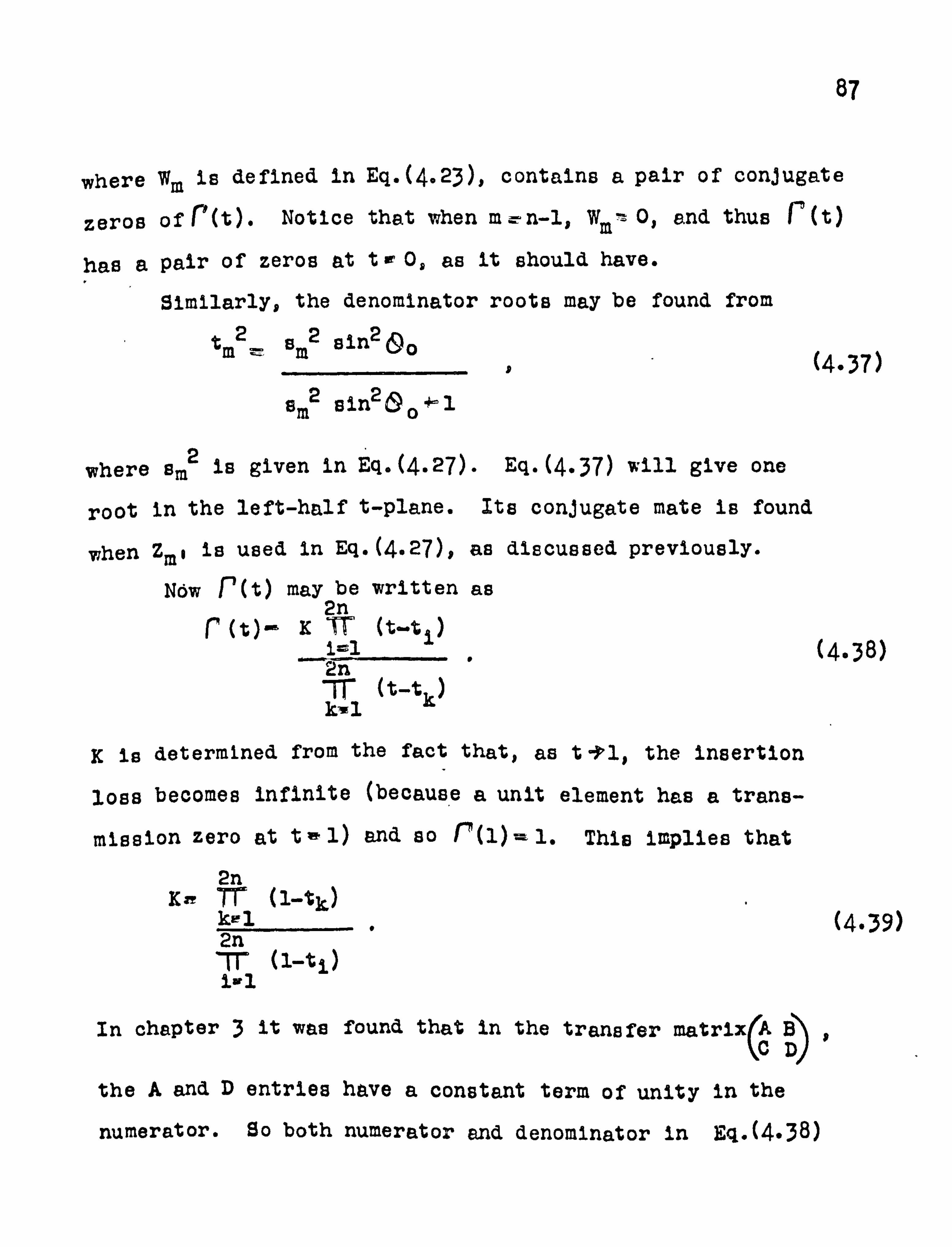
87
where Wm is defined in Eq. (4.23), contains a pair of conjugate
zeros of r(t). Notice that when m= n-l, Wm! t 0, and thus r (t)
has a pair of zeros at tr0, as it should have.
Similarly, the denominator roots may be found from
tm2ý, sm2 sing &o D
sm2 sin2o0 4°1
where amt is given in Eq. (4.27). Eq. (4.37) will give one
root in the left-half t-plane. Its conjugate mate is found
when Zmo is used in Eq. (4.27), as discussed previously.
Ndw ['(t) may be written as 2n
(t)- K T(t--ti) i=l 2n "1 (t-tk) kvi
K is determined from the fact that, as t'1, the insertion
loss becomes infinite (because a unit element has a trans-
mission zero at t v, 1) and so P(1) - 1. This implies that
2n Kn rr (1-tk)
ke 1 2n it (1-t1)
In chapter 3 it was found that in the transfer matrix kB D
the A and D entries have a constant term of unity in the
(4.37)
(4.38)
(4.39)
numerator. So both numerator and denominator in Eq. (4.38)
88
are next multiplied by a factor which leaves the constant term
transfer matrix is in the denominator equal to 2. The (C B
formed, and then unit elements are extracted as shown in chapter
3 It is easily shown that the lossless network is antimetrica1C10)
(B(t)s C(t)), and so
Z2n-i 1/Zi , 4.40)
and only the first half of the network need be computed.
In the computer program that was written to implement
the above procedure, the mapping
Z2= 1+ kltantoo (4.41)
t2
and cross-linking were used to improve the computational
accuracy, as discussed earlier. Up to twenty-element filters
were synthesized in this manner, with four and five place
accuracy being maintained throughout. The results from this,
computer program are shown in Tables 4.2 to 4.11. The label
L(DB) gives the maximum attenuation of the filter, which occurs
when O, ( 2 nT en«0,1,2, .... . kl was adjusted empirically
when extreme input specifications were desired to give the re-
quired accuracy. It was found that 1k1<3 was the best range
to use. To verify the correctness of the tables an experimental
distributed filter was built in coaxial form. The design was
! TFº INfr NC}S qº 2. L I*N º1LTINS
2 VAWN . 1.01
W 0.01 0.00 0.03 0. W 0.03 0.06 0.07 0.08 o. 09 0.10 9. to I. (ce) 38.13 06.10 19.10 14.22 10.56 9.90 s. A o. 1, 3. m ". I. one
1 12.7011 6.3326 º.
NOS 3.1911 . 9.5706 2.56n 5.9908 1.6917 1.9393 1.0071 9.90E9
Y 0.70 0, b 0.50 0.60 0. A 0.80 0.90 1. m 1.10 1,00 I, p
L(m) 0.06 0.01 0.01 0. m 0. m 0.00 0.00 0. m 0. m 0.00 0.00
1 1.9466 1.0066 1.0171 1.0121 1.0098 1.0070 5.005 9 1.0090 1.004 1.0038 1.0038
w. f Vita . 1.01?
!Y 0.05 9.02 0.03 0.08 0.03 0.06 aot 0.09 0.09 0.90 0.10
1(80) 88.99 32.07 09.00 80.07 96.26 15.80 10.79 9.61 6. a 8. 'A 0.66
º 17.9177 B. 939e 3.9738 8.6096 3.9952 3.0038 9.9890 . alt 9.0755 1.9113 1.2179
99 0.30 0.80 0.50 0.00 0.70 0.60 0.90 9.00 1.10 1.20 1.30 L(GO) 0.1ý 0.03 0.02 0.01 0.01 0.00 0.00 0.00 0.00 0.00 0.00
1 1.0946 1.0531 1.0360 1.0263 1.0163 1.0144 1.0118 1.0100 1.0086 1.0076 1.0068
. f 9982.1.05
OY 0.10 0.00 0.30 0.80 0.70 0.60 0. A 0.90 0.90 5,00 1.10
1(1e) 10.03 3.00 0.79 0.27 0. It 0.06 0.03 0.02 0.01 0.01 0.01
1 2.8378 1.5321 9.0023 1. na-? 1.0669 1.060 1.0156 1.0359 1.0293 9.0447 1.0811
e. 2 »WIR . 1.10
eY 0.10 0.20 0.30 0.00 0.50 9.60 0. A 0.00 0.9 0 1.00 1.10
1(00) 17.89 6.01 9.07 0.97 0. w 0.23 0.93 0.06 0.06 0.0* e. 03
º 9.9137 0.0302 1.0801 1.2716 1.1737 1.1213 0.0908 1.071: 1.0Y IB 9.0890 5.0020
M. f VINX . 1.90
OY 0.10 0.89 O. 30 0.00 O. w 0.60 0.70 0.90 0. A 1.00 0. b L(am) 03.44 11.7! 3.90 00.62 0.13 0.79 0.06 0.29 0.20 0.00 0.11
1 3.0691 2.7530 1.9012 5.5295 1.3023 1.2396 1.1789 1.1395 1.113! 1.09'50 5.005'
e. f 9Wý. 1.90
Y L1ý)
0. l
30. ý2
0.20
18.89
9.30
It, 77 o. 7. M6
o. io 0.69
0.60
f. 9/ 6. A
t, 97
0. t0
1.30 0.90
0.01
9.00
0.67
0.90
0.39
1 0. IM6 4.0917 !. 7609 2.1207 1.7633 1.3883 1.129 1.3276 1.2679 9.1280 /. 1109
0.2 9200.2.00
eY
LOS) 0.10
35.16 0.00
03.12
0.30
16.31 0. b
11.66 0.90
8,34 0.60
9.96 0.70
". ei 0.90
3.11 0.00
2.71 0.00
1.76 1.10
1.39
1 10.7180 9.3716 3.6187 0.7853 9.4428 1.9038 1.7121 1.9666 9.0639 1.3699 1.3399
TABLE 4.2

ETP 1106WICIts 11Y U. YW Y1 /IL1t1
1 1.6 VlW11 . 1.01
w 0.01 o. 02 0.03 0.00 0.05 0.06 0.07 0.09 0.09 0.10 0.20
LOW 137.6Y 1 17.56 99. Y7 69,47 61.72 73.38 70.03 63.39 61.29 57.63 )). 32
1 11.1u12 20.6612 13.9197 10.4316 9.3792 6.9914 6,0096 7.2683 6,6962 4,2399 2.2239 f 0.0107 0.0214 0.0321 0.0423 0,0536 0.0615 0.0754 0.0$64 0.0975 O. lep7 e. 2207
$0 0,30 0.40 0,50 0.60 0.70 0.60 0.90 1.00 1.10 1.20 1")0
9.106) 19.64 9.01 3,62 1.31 0.38 0.1] 0.03 0.02 0.01 0.00 0.00
1 1.5900 1.3079 1.1602 9.0657 1.0003 1.0301 102116 , 1.0166 1,0109 '. 009% I, OO60 t 0.3696 0,5320 0.700' 0.8,90 0. `u46 ' 0.4-55 0,96 0 0.6*, 0.9M1 0.9970 0 9960
0.6V "W" . 1, U:
90 0.01 0.02 0.03 0.00 0.0`, ' 0.06 0.07 0.00 0.09 0.10 0.20
It L9) 143,62 119.54 1 05,45 'K. A 1 87 . 70 89.56 76.01 11.37 67.27 67.61 )9.00
1 50,795\ 15.1'; 65 16.7206 12.5399 10.097] 6,0164 7.2238 6,3331 5.6906 4.0977 2.6 00 2 0: 1091 tl. U1N3 0.0274 0.0366 33.6610 0.0350
. 0663 0.0716 0.013 0.09P4 9. I. t\
pw 0.10 0.90 0.50 0.60 0,70 0. ý0 0.90 100 1. to 1.20 I]0 1(DO) 85,38 15.11 8.99 3.16 1,73
I 0. \9 0.19 0.09 0.07 0.00 0.01
1.9009 1.0013 1,279 1,167'r 9.0975 1,0614 1.0012 1.0292 I. OP1p 1.0170 9.0137 O 9.3033 8.0323 0.1763 0.7169 O, RP61 o. R96 0.9]76 0.9621 o. orto e. 9,61 e. oa2e
"Y 9631.1.05
NOW 0,10 0.10 0.70 0.00 0,50 0.60 0,70 O, b 0.90 1,00 1.10 L(0) 71,96 07.37 33.20 13.16 95.43 9.40 5.02 2,76 1.06 0.66 0.21
1 6,3\51 3.3109 1,3039 1. ß0P6 1.3177 1.3396 1.2237 I. IYf9 1.1020 1.072 3.0393 0.0757 0.109 0,2407 0.3361 0.9030 0.5999 0.67! [ 0.7212 0.0586 0.9101 0.066
N. º 9300.1.10
pY 4,10 0.00 0.10 0, Y0 O. Stl 0.60 0.70 0.90 0.90 1,00 1.10 (f! ) 77.76 53.15 39.910 2X, 91 f1,16 1\. 9] 9.70 5.15 3.09 9.53 0.77
1 7.949 0.0061 2. 'l6ä0 2.9308 1.7785 1.5116 1.3633 1.2126 1.1953 1.1476 1.1017 f 0.0667 0.105 0.4069 0. t"5Y 37/S 0.9661 0.5677 0.6706 0.7649 0.0011 0.0970
M. \ 93110.1.293
29 0.10 0.20 0.30 0"b 0.50 0.60 0,70 O. b 0.0 ". 00 1,10 L(L6) 8Y. w 58.74 u"K 0.61 26.70 20.37 u, ß9 l0. \6 8. P2 4,07 2,7
1 9.6772 6,31,5 3.1734 2.1907 2.1212 1.8.6 1.6123 1.4616 1. Nw0 1 2661 ß 20b2 f 0.0141 0 , IloS , 1925 , 7491 0.32 99 0.399D 6.6831 0 9726 O. K, YO
, 0.7111
. e. a? N
N. e 9361 . 1.50
99 0.10 0.20 )0 0 : . 40 0,30 0.60 0"A 0.40 0.90 1,00 1.10 . (t ) 64.69 65.70 1 6 53 YI. SY )). 76 27.37 11,96 17.11 1t. Y9 9,6) {, º7
1 13.2770 6. h\ß 6. \ßd1 ]. 4101 2.7711 2.3517 !. 0370 1. NOP 1.673 1.1Ke 1. YY@ O 0.0331 0.1020 0.1624 0.2200 0,2806
. 1450 0.4176 0.4,931 0.56\4 0.052 8.7761
N"" 9306.1.00
So 0,10 0,20 0,30 0.90 0.30 0,60 0.70 0. m 9o 1.00 l. lo Lllý) M"K 710.56 76,02 46,37 30,53 32.09 26.6t 09.. 17.62 13.10 90.36
/ 1{, 7812 6,8229 5.6508 6,2750 3,4573 2.9tß 2.5776 1.2162 2. gYa 1.16ßr 1. "711 1 O, g10 0.3006 0.1302 0.10ßj 0.2661 0.7233 0.3079 O. º5\1 0.1237 0.1667 416 ß)
TABLE 4.3
a+cr II !t rcn ft 6-E .* rt PTL? s
31 .6 VSMI. 1.01
BW 0.05 0.06 0.07 0.08 0.09 0.10 0.20 0.30 0.60 0.50 0.6r Lite) 150.96 1 41.44 1 33.40 1 26.44 120.30 1 99,80 78.61 97.39 62.83 30.62 to. ?I
1 10.6590 ,
51.5935 7.6341 6.6910 5.955*9 5.3764 8,7762 1.9090 1. WS 1,3473 1.2999 t 0.0396 0.0476 0.0556 0.0637 0.0717 0.0790 0.1637 0.25597 0.3546 0.9625 04739
7 31.2262 26.0099 22.2638 19.9875 17.3119 15.5699 7.6977 5. (299 1.6589 0.7959 P. 1-57
tY 0.70 0.50 O, A 1.00 1.10 9.00 1,30 1.99 1.50 1.60 1.7
6498) 12.59 6.23 x, 33 0.72 0.22 0.07 0.02 . at 0.00 0.00 0.00
1 I. 938º 1,0055* 1,0522 1.0323 1. OZ10 1.01º5 1.0106 1.00P1 1.0065 1.0056 1.009 P 0.6141& 0,7934 O, r'PR 0.9327 0.96394 0.9107 0.9901 1.9963 0.99"6 1.0007 1.0011 3 1.7532 1,6315 1,2235 1,1112 1.0562 0.9098 1.0158 1.0029 1.0050 1.0020 1.0017
r. 6 9288.1.02
ow O, OS 0.06 0.07 0. OB 0.09 0.10 0.20 0.70 0.90 0.50 0.60 L100) 156,9P 89.61 139.38 1 32.62 126.07 920.78 84.59 67.75 9P. 21 76.39 06.66
1 12.3764 10,3x; 2 8.8580 7,7604 6.9079 6.2269 3.1905 21 21%6 1.7959 +-9976 1.7220 t 0,0356 0,092H 0.0899 0,0571 0,0644 0.0716 0.1460 0.2255 0.3117 O. 9e0- 0.5037
7 79.0000 26.7917 24.3291 01,2797 16.9059 17.006P 0.8297 6.5730 4.0525 .
t"6 2. ºv 9
80 70 9 030 O. yO I. OD 1.10 1.20 1.30 0.60 1,500 1.60 1.
L(p6) 185 :
' 11.36 7.82 2.35 0.80 0.26 0.09 0.05 0.01 0.00 0.00
t 1,2167 1.1454 9.0961 9.062'1 1.0617 1. @519 1.9211 1.0162 1.0130 1.0109 1.0096
t 0,6u5b 0,7072 0.0014 0.11783 0.9301 0.9623 9P O4 0.999 0.996" 1.0006 1.0025 7 2.0256 1,6632 1.3935 1.2140 1.11111 1.0556 1.0317 1.0177 1.0099 1.0097 1.0077
r. 6 9900.1,05
rr 9.98 0,10 0.30 0.90 0,30 0.60 0.70 0.90 0.90 +. 00 1.10 L(00) 120,61 92,67 71.19 56,03 99.22 39.98 26,17 1&9P 12.5' T. 29 3.50
I 7.6.500 3.9057 2.6741 2.0775 1,7361 1.5168 1.3798 1,2653 1.1962 1.1395 1.0-93 O 0.0627 0.1271 0.1947 0.2668 0.3639 0.4261 0.5125 0,6019 0.6919 0.7785 9. '592
7 IN, 91n0 9.4006 6.19149 4.5736 3.5762 ?. 8912 1.3943 1.9906 1 6'120 1.1336 1.251
O. 6 '130.1,10
rr 0,10 0,20 0,50 O, b 0.50 0.60 0.70 0.110 0.90 1.00 1.10 L(O6) 138.87 98.29 77.01 61,86 50.06 40.30 31.90 24.69 18.02 93.87 7.57
1 9,1711 8,63117 3.1509 2,0279 0,0007 1,7299 1,5128 1.9099 1.3117 1.231+ 1,1716
t 0,0573 0,1161 0.1770 0.2111 0,3091 0,35112 0,6613 0.5369 0.6189 0.7019 0.190 3 20.3321 10.1166 6,61,75 4.9530 3.894, 3.1723 1,6616 2.2703 1.9007 1.67226 1.91<1
N. 6 93911.1.60
Or 0.10 0,20 0.30 0.40 0.50 0.60 0.70 0.10 0.90 1.00 1,10
L(Or) 180.07 103,69 02.65 67.51 53,695 45.91 37.62 30.33 11.11 17.91 12.63
1 11,1235 3.606, 3.7969 2.1909 2.3646 2.0226 1.7959 1.6135 1.8965 1,3419 9.3963 It 0.0537 O. 1683 0,1644 O. 229 0,21163 0.34119 0.4169 O. 8107 0.5629 0.6396 0.717 3 21.66 -so 10,5.005 7.1524 5.3190 4.1932 3.1761 8.8796 2.6521 2.1100 I. "291 9.5'52
r. 6 9800 . 1.50
!r 0.10 0.20 0.30 0.90 0,50 0.60 0.70 0.110 0.00 +. 00 1.10 L(la) 197.06 110.08 09.64 74,50 62.67 52.93 99.61 37.71 30.79 91.116 18.62
1 19,7949 7,4278 0,9902 3,7630 3.0675 2.9971 0.2679 9.0258 1.199 1.6462 1.! 909 ! 0.0515 0.1035 0,1566 0.11113 0,2690 0.3272 0.3890 0.4537 0.5213 0.9910 0.6650 3 03.456 11.6527 7.7289 5.7538 4,3975 3.7495 3.1628" 2.7130 2. )56) 1.063+ 1,8176
r"6 9086.7,00
08 1(11)
0.10 151.6)
0.20 115.63
0.38 98.61
0, YO 79.17
0.50 67.98
0.60 57.70
0.70 19.38
0.80 611.08
0.90 35.53
1.00 89.61
1. +0 1416
1 16.7286 9.7'12 6.09551 8.7562 3,5151 3.2555 0.6067 0.9925 6.930 05 6.9+ +. 9052 ! 0.0328 0. IWB 0.1587 0.1871 0.26% 0.3299 0.3889 0.6527 0.3160 8.5675 0.6590 7 14. &º1 1!. 600! 6.1509 6.0796 6.8188 3-M 3.7601 1.8968 11.3203 1.11193 1.9658
TABLE 4.4

$7! f INMD MCA! R 54LDI Nr IIL1W
.8 1» . 1.01
am 0, % 0.06 0.07 0.08 0.09 0,10 a. RO 0.30 0.40 0.90 0.60
1(s) 819.67 207.00 196.19 187.00 176.81 171.49 123. q 98.99 78.60 58.19 45.86
1 11.6493 9.7165 8.3803 7,301'2 6.9060 S. 666T 3.0167 20023 1.6703 1.6301 1.149 R 0.0360 0.0431 0.0503 0.0578 0.0651 0.076 0.9877 0.9308 0.3156 0.8 9 0.962 3 35.4720 29.3519 05.3220 21,1405 19.6790 17,70241 8.7831 3.7754 6.2427 S. 19" 9.6309 º 0.0561 0.0316 0.0366 0.0619 0.0471 0.0524 0.1093 0.1593 0.2157 0.2751 6.3392
!Y O, 'N 0. -W 0.90 1,00 1,10 1.20 1,30 1,40 1.50 1.6C 1.70
1(00) 34.72 84.96 16.99 6.82 3.46 0.97 0.06 0.06 0.02 0.00 6.00
1 1.1903 1.12,11 1.0850 1.0565 1.0362 1.0x31 1.0153 1.010 1.00"1 1.0060 1.0091 f 0,6039 0.6977 0.7835 0.9379 0.9171 0.9567 0. V1'" 0., 9D4 0.9%3 0,9907 1.0016
2.1742 1,11) 1.53x1 1,3,89 1.1687 1.0810 1.0313 1.01"7 1.0096 1.0013 1.0032 º 0.4106 0.4906 0.3696 0.7032 0, Rpm 0.9087 0.9575 0.91'0'1 0.9916 0.9966 0.9W9
P. 6 9068.1.022
rY 0.09 9.06 0,07 0. ON 0.09 . 10 0 a20 0.30 0. °0 0.30 a. 68
L(D) 829.63 211.96 204,26 19x. 98 181,79 17186 . 1280 100.17 : 0.66 6i. °6 31.08
1 13,3434 11.1326 9.5316 8.3666 7.4W 6,7109 3. WA 2.3 9 1. ̀ . '370 1.56'1 1.3 9° t 0,0329 0.0396 0.0462 0.0528 0.0596 0.0662 9.93" 0.5067 0.2''81 0.3663 0.0340
"º 37,6086 0.0246
31.5636 0.0298
27.0174 0.0347
93.6599 0.0397
01.0732 0.087
1'.. 9133 0.0496
9.3976 0.0991
6,1963 0.1W
8.5712 0.2034
3.3749 O. P904
8.1909 0.316"
rY 1(D)
0.70 40,70
0,00 30.93
0.90 02.99
1.00 14,33
1.10 7,63
1.20 8,99
1.30 0. q'/
I. W 0.23
1.50 0.06
1,60 0.00
1. '10 0.00
1 R
º
1.2722 0,5435 0,3922 0.3603
1.1919 6.6326 0.009! 0.4512
1,1356 0.7179 1,7065 x5325
1.0953 0.7966 1.0678
' 0.6277
1.06599
. 0.8658 1.2030 0.7339
1.0687 0.9215 1.1528 0.8622
9.0308 0.9593 1.11736 0.9197
1,0213 0.9"7.12 1.0373 0.9625
9.0161 x9930 1.0191 0.9036
1.0171 0.990 1.0101 0.9932
1.0107 1.002' 1.0060 0.9279
M"8 98611.1.05
eY
1(09)
0,20
137.08
03)
97.89
0.50
72.70
0.63
53.90 a. CO
30.76 0.9,
15.93 1,10
18.8, 1.23
5.813 1.40
1.23 1. y1
0.1°
7.70
0.813
1 6 3 6
8.9876 0.111,
1ax1iº 0.0937
2.4635 0, x161 3.7563 0,1657
1.0233 0.3210 3.9364
" 0.2408
1.5e7 0.4348 2.9i"y 0.3211
1.3196 8.5ii3 2.2699 0.4104
1.207, 0.6703 1.9076 0.5144
1.1342 0.7'. 73 1.4696 0.6810
1.0.30 0.8939 9.2297 0. rgs
9.0530 0.9563 1.0.0 0.9161
1.0353 0.99,9 1.0367 c. 973!
1.8553 1.00+0 1.0159 0.9916
r. 0 98611.1,10
OY 1(D)
0.70 IM. 86
0,35 103.71
0.30 72.52
0.65 59,72
0. Flo 44.57
0.95 31.74
1.10 20.32
1.23 10.71
1. io 3.32
1.53 0.67
1.781 0.11
$ e 3. i
6.8669 0,1173
lae»9 0.0901
0.8782 0,1997 6.1139 0. lsvl
0.0958 0,2945 8.2073 0.4! 06
1.69h 0,3970 S. 1488 0.3060
1.4657 0.3 61 0. iý3i 0.3080
1.305 0.6107 1.9121 0, ºHOº
1.2201 0.7301 1.6228 o. 1094
1.1113 0.: 352 1.3517 0.7196
1.1014 0.3055 1.1651 01:
1
. sn
9.0607
0.9611
1.060
e. as0"
1.0603
1.0137
1.0319
e. 4A°6
r. 6 9866.1,80
OY
L(D)
0. R0
180.50 oao
109.35
O, w 06.16
0.63 65.37
0.80
Mat 0,9,
37.39 1.10
56,93 1. x1
18.09 1. %0
7.87 Ls9
2.06 1. `e
IL 14
1 R
º
5. BTÜ 0.103A
17.0639 0.0879
3,6266 o, 1&s 0.3021 0.1563
6.4703 0. x768 4.411), 0.8230
1.9730 0.3705 3.3732 0.2910
1.6768 0. ºtlo !, 6602 0.3719
1. %rm 0.5766 2.1567 0.4565
1.3526 0.6943 1.7801 e. S529
1.43"1
0.14141
1,8982
0.6661
1.1778
0. "" 8
I.. 7 l o. Tý163
1.1350
1.9764
1.1265
0.0150
1.108
1.0461
1.0401
w9'1K
r. e 96Ye . 1.30
eY L(D)
OiO 555,49
O, u 116.34
o. w 91.15
0.6s 72.36
0.60 MIS
o. 9s 44.37
1,10 33.12
1.25 82.98
1.40 13.79
1,35 6.07
1. 70 9.63
1 I 3 f
7.7823
0.10,30
4547 10.0956
1.4996
7 0,1841
0.1908
3.2060 0.8681
0: t
5.5250 0.3572
O. x664
2.1090 0.4313
O. J39P
I. P339 6.5515
o. iJ 7
9.6106
0.6362
e1. g9r.
. 5260
1.8967 0,7639
0.62381
1.3901 0., 72,
0.7779
1.3037 x9799
o. RP609
1,2388 1.0681
0.9611 r. 0 96161.1,00
fY 0.20 0,33 0. w O. y x80 0.93 1. w 1. x5 Lie Lyy 1. ie 1(D) 160.26 101.11 95.91 77.13 61190 89,15 37,89 17.78. " 14.88 10.05 3.73 1 0.8808 3.6904 4.0307 3.1693 2,6082 2,2855 1.9673 1,7956 1.6873 1,3279 t. º36 e 0.1077 0.1905 0.8766 0.3665 0.4628 0.8633 0.6699 0.7 92 0. °%1 1.0! 33 1.1235 3 13.3727 7.5919 5.2588 3.9852 3.1741 2.6059 2.1616 1.9590 1.5964 1.3761 1.2296 4 0.0854 0,1104 0.1168 0.2834 0.3572 0.41337 0.5166 0.6098 0.718? 0. °331 0.6873
TABLE 4.5

ern : wcwnZ$ of Io. LDOW Hama
11 . 1u vswn. 1. o5
90 0.30 0.00 o50 0.60 0.70 0.00 0.90 1.00 1.10 1.20 1.30 14io) 106.00 120.76 101.00 62.70 10.75 58.50 47.52 37.52 26.30 19.71 11., 2
1 2.9134 2.2524 1.8702 1.6267 1.1619 1.305'1 1.2616 1.1991 1.1519 1.1157 1.0671
2 0.1706 0.2432 0.3117 0.3839 0.65'3 0.5363 0.6135 0.6886 0.7597 0.8269 0.11030 3 6.9658 5.1823 0.0666 3.3391 2.7952 2.37l5 2.0690 1. '1935 1.5681 1.3936 1.2939 i Y. 1, /63 0.1031 0.2312 0.2811 0.3334 0.3891 0.4493 0.5153 0.9488 0.6710 0.7620
S 7.5646 5.6357 0.0688 3.6821 3.1116 2.6746 2.3254 2.0309 1.7809 4.9635 1.3665
11.10 V308 . 1.10
PV 0.30 0.40 0.50 0.60 0.70 0.90 0.90 1.00 1.10 1.20 1.30 L(t$) 151.86 126.59 106.82 90.52 76.57 64.32 93.34 43.34 34.11 23.49 17.42
1 3.4019 2.6091 2.1460 1.8172 1.6120 1.0909 1.3861 1.5058 1.2000 1.1005 1.1507 2 0.1667 0.2162 0.2öt+N 0.3545 0.1233 0.6961 0.5670 0.63117 0.7104 0.7749 0.5625
7.3883 5.4918 1.3005 3.5611 2.9910 2.5601 2.2162 1.9372 1.7076 1.51010 1.1617 4 0.1327 0.17111 0.2246 0.2725 0.3224 0.371111 0.0307 0.4911 0.5972 0.6300 0.7117 5 7.7997 5.80.41 1.6106 3.8007 3.2217 2.7772 2.0237 2.1322 1.4041 1.6666 1.4721
9.10 VSV6 . 1.20
Ow 0.30 0.40 0.50 0.60 0. TO O. 00 0.90 1.00 1.10 1.20 1.30
L(06) 157.50 132.22 112.06 96.16 82.21 69.96 58.90 09.19 39.75 31.13 23.01
1 0.0666 3.0975 2.5263 2.1569 1.0947 1.7110 1.5701 1.4616 1.1765 1.3005 1.1533 2 0.1591 0.2152 0.2737 0.3348 0.2`216 0.6650 0.5335 0.6033 0.6738 0.7426 0. ^097
7.8304 5.8292 6.6170 3.79'5 3.2109 2.7515 2.5933 2.1001 1.8290 1.6554 1.0152 1 0.13117 0.1752 0.2007 0.2673 0.3156 0.3660 0.9191 0.4756 0.3366 0.6012 0.6766
7.9971 5.9666 0.7005 3.9164 3.3210 2.8690 2.5108 2.. 176 1.9697 1.7509 1.5600
0.10 VSVR . 1.50
YV 0.39 0.40 0.50 0.60 0.70 0.80 0.90 1.00 1.10 1.20 1.30 6(00) 164.49 139.21 119.45 103.15 89.20 76.95 65.97 55.97 46.74 39.11 29.99
1 5.3610 4.0591 3.2762 2.7777 2.4201 2.1569 1.9563 1.7994 1.6740 1.5722 1.6'1e1 0.1579 0.2125 0.2693 0.3210 0.3295 0.4'531 0.5191 0.52'71 0.6567 0.7270 !. 991'3
3 1'. 5621 6.301'9 5.0650 0.17'72 3.5366 3.0483 2.6622 2.342"1 0.6871 t. 'ä69 1.6795 i 0.1710 0.17,6 0.2209 0.2672 0.3149 0.3602 0.4157 0.4699 0.5276 0.5^91 0.6561 5 8.2570 6.1641 6.9014 4.0536 3.4426 2.9791 2.6136 2.3159 2.0665 . 1.8525 1.6645
11.10 V2AR . 2.00
NW 1-. 30 0.40 0.50 0.60 0.70 0.110 0.90 1.00 1.10 1.20 1.30 1(00) 169.26 103.98 121.22 107.92 93.97 0.1.72 10.75 60.75 91.51 02.49 30.75
1 6.6132 5.1614 4.1454 3.0871 3.516 2.6764 2.1122 2.2036 2.0353 1 ? 973 1.771 2 0.1660 0.2233 0.2322 0.3011 0.0059 0.4712 0.5389 0.60, " 0.6912 0.7553 0. -347
9.3253 6.9564 5.5256 6.5634 3.6697 3.3409 2.9206 2.5259 2.3069 2.0664 1.5635 i 01303 0.1790 0.2262 0.2734 0.3219 0.3719 0.0238 0.0770 0.5352 0.5961 0.6614 5 8.4564 6.3161 5.0262 4.1573 3.5329 3.0600 2.6875 2.3? 49 2.1325 1.91°0 1.77°9
TABLE 4.6
! Rp r"MOAPM Oº IS-L I? VUJTW
. 12 v$ . 1.05
W U. 3D U. OU U. SO 0. fu 0.70 0. iu 0.90 I. W 1.10 1.20 1.30
L(M) 163.19 152.94 199.81 109.64 90.69 76.18 66.90 52.96 81,86 31.66 11.79
1 9.96.6 0.2681 1.6961 9.9499 1.8903 1.3616 1.2746 1.2105 1.1960 1. It69 1.0961 t 0.1760 0.2397 0.39170 0.3776 0.4516 0.3972 0.64! 9 0.6767 0.7665 0.8106 0.8675 3 7.2064 5.27" 6.16113 3.6465 1.8557 2.41361 2.1013 1.1339 1.6159 1.694* 1.6997 6 0.1342 0.164 0.9273 99.9761 0.3970 0.3909 o. $387 0.5013 0.5699 0.6454 0.7479 S 7.7693 5.79 3 6.9976 3.7930 3.2110 0.7669 1.4136 3.1828 1.0766 1.6588 1.0655 6 0.1282 0.1719 0.9165 0.9962 0.3998 0.3586 0.6106 U. 4656 0.3737 9.5930 0.6709
P. I2 9991.1.10
IV U. 3u 0.00 0.59 0.60 0.79 0.60 0.90 I. W 1.10 Lou 1.30
L(a) 169.11 159.76 135.04 115.46 90.71 89.190 70.40 56.74 67.68 37.30 73.91
1 3.6555 1.646 2.1768 9.8723 1.66.9 1.3126 1-4013 1.3171 1.6611 1.0011 1.1606 t 0.1651 0.2246 0.! 660 9.35ui 0.4166 0.4667 0.560! 0.6316 0.7019 0.7626 0.0311
3 7.7W6 5.9809 6.8130 3.6234 3.0696 2.6106 11"2633 1.9617 1.7506 1.5598 1.6039 º 0.1316 0.1765 0.2224 0.9697 u. 316i 2.370! 0.6946 0. M3u u. Sº6e 0.6151 0.6903 S 7.9791 5.9523 8.7266 3.9055 3.3112 !. 8930 !. 5007 2.9070 1.9590 1.7860 1.5536 6 0.1260 0.1606 0.11126 0.9371 0.3030 11.3506 0.19494 0.9329 0.5098 0.307 o. NW
. 1! Y2YLL .L to
sm 0.30 0.40 0.31 0.60 1). 70 0.011 u. 30 I. w 1.99 I. Vi 1.30
1. (D)) 194.75 164.41 160.66 111.11 904.35 89.66 76.66 64.41 53.32 49.96 33.15
1 4.1293 3.9N9 9.5669 2.1066 1.9036 1.7323 1.3665 1.6776 1.390 1.3216 1.9656 t 0.1566 0.9994 0.8'726 0.3333 9.3966 0.6625 0.3308 0.5995 0.6668 0.777! 0.903 3 7.957! 5.9057 0.6951 3.2649 3.26.9 2.6037 1.6401 t. 1N7 1.9093 1.6961 1.5953 4 u. 13u6 0.1751 u. 2au5 0.9670 0.3150 0.3649 0.4173 0.6729 0.3393 0.3968 u"9666 S 9.2Wt 6.1904 4.8650 8.1918 3.4137 2.9501 2.5876 9.2691 2.0399 1.8269 1.63%
u. 12N 0.166 0.9.16 U-0535 0.2993 0.3449 0.39322 U. 413E 0.1974 0.5550 0.6166
M. 1! 1991 . 9. Su
M 11 319 U. W 0.5u 0.60 U. 70 U. 6u U. 9U 1.04 1.10- 1.20 JU 4. ) 101.74 171.39 147.67 126.10 111.34 96.63 83.113 71.41 60.31 69.93 80.64
1 5.6518 4.1256 3,3393 1.64u6 9.41563 1.1979 1.9833 1.8232 1.6953 1.5916 1.505" t 0.1519 0.1141 0.9710 0,3301 0.3915 0.6558 0.5213 0.5196 0.6590 9.7295 0.890 3 8.7553 6.5979 5.1617 4.1754 3.6803 3.1230 2.7246 2.9661 2.1618 1.9186 1.7266 º 0.1331 0.1763 0.2242 0.9711 0.3194 0.3693 0.4012 0.4756 0.5339 0.9967 0.6607 S 6.55]6 6.6670 S. Uiu6 4.1031 3.5714 3.0997 2.71% 9.6090 2.153! 1.9367 1.7439 6 0.1233 0.1{56 u. tu79 0.1592 9.1956 0,3412 0.3883 0.4374 0.0689 0.5436 O. 6ut3
M. 1t 929 . t. UU
641 0.30 0.1b60 0.50 0.60 0.70 0.6U 0.90 1.00 1.11 1.20 1.30 LOS) 206.59 176.17 152.64 132.07 116.11 101.90 86.11 76.16 65.00 54.70 66.91
1 6.9636 5.2385 4.1202 3.5503 3.0751 1,7133 2.6523 9.83B9 !. 069 1.9e59 1.6066 2 0.1686 0.9266 0.2965 0.3481 0.8119 9.4781 0.3*66 0.6175 9.6115 0.7653 0.6611 3 9.6332 7.1669 5.7097 4"7165 3.9995 1.4331 3.0136 !. 6768 9. ]971 !. 1626 1.9360 6 u. 1397 u. 1838 0.2336 0.5886 0.3313 0.3636 0.4372 0.6199 0.5516 0.6136 0.6795 S 2.9104 6.6547 5.2946 6.3883 3.7253 3.5291 9.6370 2,3156 2.6633 2.096 1.6364 6 0. uii O. KSi 0.1063 0.6617 0.1904 O. NtS U. 388* 0.1371 9.8879 0.5615 0.3986
TABLE 4.7
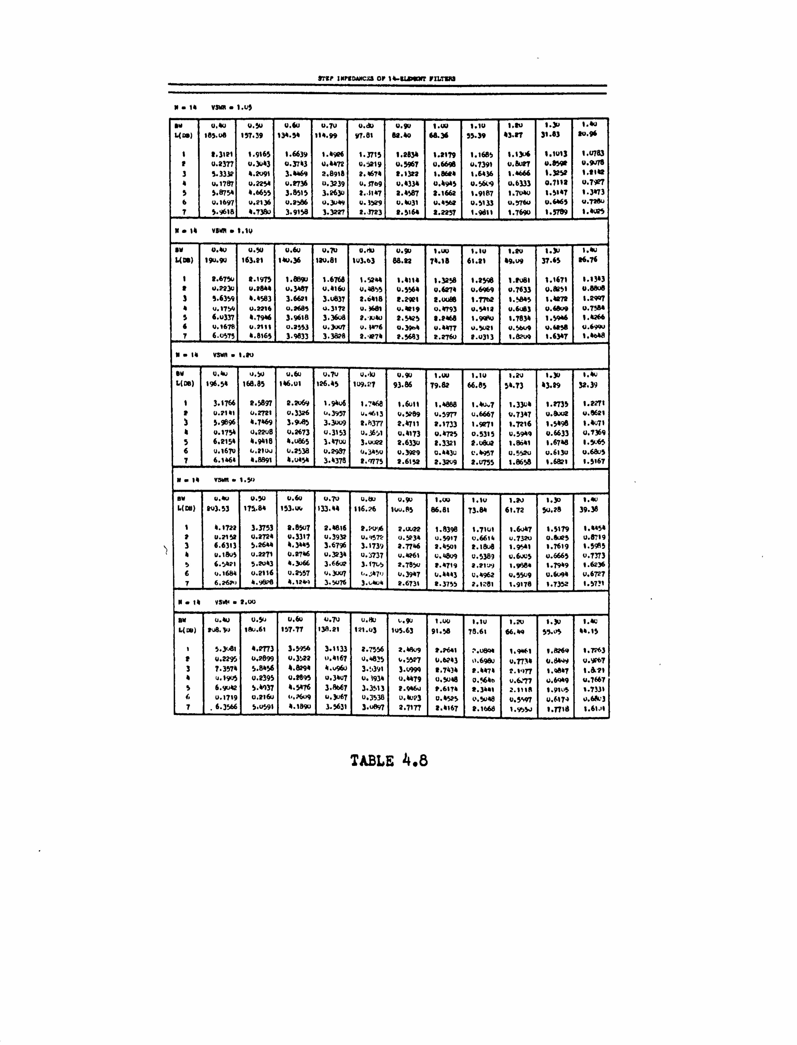
IMP IMKDAPCZS OF I4-9D I? IILTW
N. 14 Y3WR . 1. Vý
W U. 4u Q. 5u u. 6(i 0.70 u. au u. qu t. w SOU 1"N 1.30 1.40 L(u5) 185.08 157.39 134.56 114.99 91. e1 69.10 68.36 55-39 93.27 31.83 20.96
1 5.3121 1.9165 1.6639 1.9986 1.3715 1.2836 1.9179 1.1685 1.1306 1.1013 1,0783 P 0.2377 0.3093 0.3763 (1.6472 0.52t9 0.5967 0.6698 04.7391 V. 8U37 8.8598 0.9078 3 5.3330 6.2091 3.6669 2.8918 2.1616 8.1325 1.8689 1.6436 1.4666 1.3252 1.8192 4 0.1787 0.2254 0.2736 0.3239 0.5769 0.6336 0.4945 0.5619 0.6333 0,7112 0.7907 5 5,8751 6.6655 3,9515 3.263(1 2. "1167 2.6587 2.1662 1.9187 1.7060 1.5147 1.3673 6 0.1697 0,2536 0.2596 0,3019 0.1529 0. M131 0.4562 0.5133 0.5760 u. 6Y65 0.7Y6u 7 9.9618 Y. 738u 3.9158 3.3227 2.1723 2.5164 2.2257 1.9811 1.7690 5.5789 1.6.185
B. 1Y 96611.7.19
Br 0.40 0.511 0.60 0.70 0.44' 0.9n 1.09 1.10 1.90 1.30 I. w
5(25) 190.99 163,01 140,36 120,81 103.63 88.22 71.18 61.21 89.09 37.65 116.76
1 2.675U 8.19T5 1,8899 1.6768 1.5244 1.4114 1.3258 1.2599 1.2181 1.1671 1.1363 f 0.223u 0.2866 u, 3967 U. 160 (1,4855 (1.9564 0.6274 0.6969 0,7633 0.8851 0.8908 3 5.6359 6.6563 3.6621 3.0837 2.6418 5.2961 2.0068 1.7762 1.5885 1.4272 1.2997 6 0.1759 0.2216 0.2681 0.3172 u. 1681 (1.69/9 0.4793 0.5412 (1.6083 0.6809 0.7586 5 6.0337 6,1966 3,9618 3.3608 2. "uw 2.5625 8.2968 1.9990 !. 7811 1.5 66 1.6266 6 (1.1676 11 . 2111 1.2553 0.3001 0.50 6 0.3966 0.6977 0. yl21 0.5609 0.6158 (1.6990 7 6.0575 6.8165 3.9933 1 3,3828 5.1879 ,:
1 9.5693 2.5760 9.0313 1.8209 1.6367 4w 1.
B. 14 4389 . 1.10
Br 6.90 0.90 u. 6u 0.70 0., 1) 0.90 1.09 1.10 1.215 1.30 1. w
1"(DB) 196.54 168.85 196.01 126.95 119.27 93.86 79.82 66.85 56.73 63.19 32.39
1 3.1766 2.5897 2,2069 1.98 $ 1.7468 1.6011 1.6888 1.69. "7 1.3308 1.2735 1.2275 I 0.2181 0.5721 0.3326 0.3957 0.2613 (1,5299 (1.597 0.6661 Q. 7341T 0.8002 0.8621 3 5.9896 6.7869 3.9585 3.30u9 2. x377 2.4711 9.1733 1.9271 1.7216 1,5496 1.4071 Y 0.1756 0.224)8 0.2673 0.3153 9.3651 0,4173 0.8725 0.5315 0.5949 0.6633 0,7369 5 6.2154 4.9415 8,0865 3.670. 3.0022 2.6330 2.3321 9.0802 1.8641 1.6746 1.5.65 6 2.1670 L, YIUJ 0.2538 0.2997 0.3450 0.3929 0.863u 2.8957 0.5520 0.6530 0.6805 7 6.14,64 8.8891 f. U451 3.4378 2.2! 75 2.6152 2.3209 Y, u755 1.8658 1.6821 1.5167
B. 16 05th . 1.51,
er U. 40 0.30 0.60 0,70 u. eu 0.90 5.00 1,10 1.20 1.30 5.96
1. (21) 903.53 175.88 153.09 133.46 116.26 109.55 86.81 13.84 61.72 5(1,28 39.38
I 1.1722 3.3753 2.8527 2.4616 2.2996 2.0022 1.8398 1,7101 1.6017 1,5179 5.6654 2 0.2152 0,2724 0.3317 0.3932 0. "1575 2.5238 0.5917 0.6616 0.7320 0.8029 0.8719 3 6.6313 5.2684 6.3465 3.6796 3.1739 2.7766 2.6501 2.1906 1.9541 1,7619 1.5985
Y 0.1805 0.2271 0.2766 0.3236 0.3737 u. 626t Q. 48V9 0.5389 (1.6055 u. 6665 v. 7373 5 6.5621 3.2043 4.30(6 3.6602 3.17L5 2.755o 2.6719 2.2119 1.9986 1.7969 1.6236 6 0.1684 0.2116 0.2551 0.3007 L.; A7. 0.3997 5.8613 0,1962 0.5509 8.6096 0,6727 7 6.262. 8.9628 4.1281 3.5076 3.11-1 2.6731 1.3755 2.1: 81 1.9178 1.1352 1.6771
II . 16 9545 " 5.00
Br U. 80 0.50 U. 60 0.74) u. OU 4,90 1.0 IOU 1.20 1.30 1.1-
L(3P) PA. 3o 180.61 157.71 136.21 121.03 105.63 91.58 78.61 66.69 5343 88.15
1 5.3o81 4.2773 3.5956 3.1133 2.7556 2.6809 2.2641 2.0e98 1.9*1 1.8269 1.7763 P 6,2295 0,2899 0.3522 ((. 6167 0.4835 6,5527 0.6283 ',. 696u 0.7798 6.86.59 0.9267 3 7.3574 5.8456 9.8294 4, u969 3.! 391 3.0969 5.7638 8.8676 2.1977 1.6867 1. &25 Y 001905 0.2395 0.2895 0.3601 u. 1936 0.6679 0.5008 0. %64. 0.6147 0.6999 0.1667 5 6.9u42 9.8937 6.5676 3.6667 3,350 2.946U 2.6174 2.3441 2.1118 5.9005 1.7331 6 0.1719 0.2169 L, 26uq 0.3067 0,3536 2,1023 5,9525 0.5048 0.5.97 0.6974 0.6203 7 6.3566 5,0591 Y. t89u 3.5631 3.0897 2.7177 2.6167 2.16 8 1.955-3 5,77t8 5.6181
TABLE 4.8

STS, 1"FrANCU or l zlyaw nLTElu
h. 16 v3WR . 1.05
1333 0.50 0.60 0.75 0. no 0.90 1.00 1.10 1,20 1,30 1.40 1. so L(OY) 103.54 159.82 ' 137,06 117,4II 99.60 93. T4 6BA1 53.04 83.93 29.4q 17.50
1 1.92y3 1,6743 1.5011 1.3706 1.2694 1.223, 1.1729 1.1346 1.1049 1.0916 1
1.0631 2 9.3025 0. ]720 0.4444 0.5+E5 0.5929 0.6655 0.7345 9.7979 0.9"J, 42 0.9023 0.9420 3 4,2399 3.4735 2.7156 2.4891 2,1574 1.8013 1.6614 1,4933 1.3412 1.2246 1. ]842
4 O. e241 0.2721 0.322, 0.3746 0.4305 0.8906 0.5559 0.6267 0.7025 0.71.44 0.1'053 5 4,7072 3.0072 3.2947 2.0436 2.4859 2.1929 1.9865 1.7303 1,54! 4 1.377) 1.2349 6 0.2123 O. P568 0.3007 0.3501 0,3996 0.4510 0.50'79 0.5621 0.6354 0.7116 0.7996 7 8,5! 14 3.9694 3,3702 2.9177 9.5570 !, 2641 !. 0199 1. '999 1.6210 1.45O5 1.! '104
8 0.2086 0.2223 0.2971 0.3473 0.5917 0.481 0.4947 0.5517 0.614S O. 6960 0. TItS
31 . 16 9696.1.10
6r o. w 0.6n 0.70 u. eo 0.90 l. ao 1. tu 1.20 1.39 t. bo t. sn L(r. ) 191,35 165.2) 18!. 08 123.23 105.62 P9.95 74.72 60.96 47,77 35.30 23.34
1 2.2121 1.9009 1.6966 1.5327 +, 4586 1.3320 1.2652 1.2129 1.1715 1. +313 1,1114 2 0,2634 0.3475 0.4143 0.4833 0.5541 0.6247 0.6939 0.7601 0. "216 0. "770 0.9057 J 4,41192 3,6355 3.1069 2.6620 0.3114 2.026P 1.7932 1.6006 1.4426 1.3147. 1.2131
4 0.2212 0.26110 03165 0.367, 0.4206 0.4775 0.33447 0.604! 8 0.6+61 0.7517 0.198 S 8,1378 3.9987 3.3926 2.9326 2.56559 2.2717 2.0221 1"472 1.61.9 1.4593 1.3096 6 0.2106 0.2546 0.3990 0,3465 0.3949 0.4456 0.4993 0.5569 0.619 0.6"99 0. '90 7 8.67349 4.0362 3.1293 2,9693 2.6070 2.3126 2.0667 1,0563 1.6715 '. 5047 1,3497 0 0.2065 [ 0.2496 0,2937 0.3390 0.3062 0.4352 0.4067 0.5418 0.6006 0.6665 0.7426
N. 16 9380.1.20
66 0,70 0.60 0.70 0.60 0.90 1.00 1.10 1.29 1,30 1.40 3.59 L(06) 197.00 170,66 146,32 127.60 111.26 9y, 20 90.37 66.50 53.85 40.98
" 97
1 2.6077 2.2216 1.9528 1.7572 1.6101 ' I. 446'1 1.4076 1.3766 8.2791 1.2323 t. 1 X33 0 0,2719 0. ]323 0.7953 0,4607 0,5281 0.39614 0.6656 0.73)6 0. '99^ 0. ^6o 0.9869 ] 4.7437 3.9396 3.3279 2.4617 2.4929 ]. 1934 1.9459 1,7392 1.3653 1.? 32 1.3057 4 0.2213 0.2679 0.3159 0.3657 0.817' 0.4729 0.5316 0.5046 0.6623 0.73"' 0.1109
4.5951 4.1313 3.5047 5.0366 2.6641 2.3608 2. +071 1.514' 1.7000 1: "x]20_ 6 0,2107 0.2546 0.2996 0,3459 0.3439 0.4437 0,4962 0.53+9 0.6520 0.6779 0. -513 7 4. X79 4.1083 3.8924 3.0060 2.639+ 2.3615 2. +t 39 I. 9n2'; t. '1'ß 1.5543 t. "036 n 0,205, 0.2470 0.29+4 0.3367 0.31126 0.4307 O. bf 10 0.5341 0.5`4! C. 052'ß 0. "223
Of . 16 Yawn . 1., 0
u o. so 0.60 0.70 0. ßw o. 90 1.00 t"w 1.20 t. lc t. a0 +. X L(00) 203.163 177, +7 135.51 175.87 11'5.25 302.19 67.36 73.49 60.40 87,93 33.06
1 3,4023 2.9730 2.1004 2.2257 2.0+61 1. ßy21 8.1230 1.6144 1.52¬7 1,4535 1.3.1- k 0,2735 0.3330 0,394' 0. "'89 0,3133 0.593' 0.6617 0.7344 0.050 0. '747 8.9432 3 7.3+66 4,3,63 3.7140 3.2121, 2.35092 2.1112 2,200 I. '5' 3 1.7.62 3,02,1. .a 13 4 0.229 0.204 0.3766 0.303 0.4303 0.85,3 0.343" u 6051 0. rn9 C. " W 0. ire
5,2YW 8.3601 3.7e65 2.34366 7,31"8 2.7538 2.16"i 1. '333 1.65" 1. "1131I 6 0.211 0.2595 0.3052 0.3.59+ 0.4004 0.4506 0.5030 0.55.1 0.616' C. 6 00 C. -4'12 7 5. IU69 4.2203 3.896"^. 3.1174 2.7822 7.437 , 2.1' SP t.. ro'1 s 1,6? 1+ I, 4t7 ^ " 0.2085 0.2469 0.2903 0.3349 0.31107 0.424 0.4775 O. 5103 0.8"4' 0.1.42'' O. "4170
. 16 Yawn . 2.90
15. 0.50 0.44 0.70 0.10 0.90 1.00 1.10 7.20 I. JO 1.40 1,340 L(08) 206.76. 142.64 160.2� 140.64 123.02 106.6 92.13 7+, 26 65,17 3, ". 70 8C. ^S
I 1,3187 3.6246 3.1420 2.7'02 2.5023 2.2'30 2.1062 1,961+ 1"'905 1"-3'8 1,6571
2 0.2f6 0.3555 0.4205 0.4079 0.5577 0.6. '9" 0.7041 0.700 0.5^. 0 0. -313 3.030' 3 5.9507 8.9160 4.1783 3.6031 3.1571 2.7945 2.8936 2.2397 ^. 0233 1, ')7 1.67)1 4 O. P443 0.291522 0.3474 0.4811 0.6367 0.5146 0.5759 0. $1,15 0.70; 7 0.1 07
y 3.6486 8.6764 3.7764 3.8869 3,0304 2.6929 2.4123 2.1'41 1,. 6" 1.7 63 1.6746 6 0,2223 0.2684 0.3156 0.3639 0.4137 0.4653 0.5199 0,5751 8.6346 0,69°1 P. -6d" 7 3.2366 ; , 3530 3,703+ 3. £114 95257 . 2.5134 !. 2544 2.0751 3.183" 1.670) 1.51340 tl 0.2051 0.2477 0.2912 0,3357 0 . 3615 0,8269 0,6759 0.5244 0. ]")S 0.6811 !. 7033
TABLE 4.9

9". it t%Wbk4 t] np iS IL ,M Pi! Aiq
N. 11 v3im. 1, OS
ti o o, A O, p 0,9i IM 1,10 120 1,10 1d ' l, y) 1, OD L(Da) IS1 J7 139.11 11TA1 117.16 99,10 aa. 0) 66,69 1. A) 6 3" m tº. 35 11.79
1 1,6915 1.5)73 1.3939 12994 12269 1.1764 1,1374 1.101, 1,0619 1,0656 1.059) t 0.395 0.02 0,5199 0,390 0,6996 0,7318 0,7966 0,9109 0.999) 0,9393 0.917)3 1 3-490 2,9727 24083 8.1664 1.6944 1.6437 I A950 1.3590 1 J399 1 , 1361 1.0916 t 11 J714 042)0 0,3732 0.1297 0.4E03 0.5599 0.6926 0.6978 0.7146 0.8509 0.9)06 7 6
3.9911 0 8
3.3159 0 0
2.9899 2,3u39 2.2096 1.9615 1,1674 1,5600 1"3959 1r551 1.1396
7 559 .
0024 \ ,3 15 0,3436 0,3.117 0,4494, 0,50" 0.59)9 0.6995 0.7199 0.7993 0,6756
a .
023)9 3.399) 02953
2.9121 0 3110
1.5916 0 9
82995 0.9309 1,11321 5.963 1.879) 1.3720 1.1790
" º. Utl9 39106 ,
1,9437 ,3 45
4 66 0,1379 0,4901 0,5456 0.1081 0.6736 0.725 0.19171
. 59 6.3wß 4.0376 1.6º9e 1.6669 1,5010 9,5099 1.1929
a", e vNº. 1.10
I'll 0.60 0.70 0. NI 0.9) I, W 1,10 120 9.91 I, w I. 9D I. 1, L3Oa) I99A9 161,9) 188,62 1! 3,044 104,90 58-12 72,2 17.69 83,91 10,36 17.39
1 1,9097 1.600 1 . 5.109 1.16,35 1.3366 1569? 1 2165 t , 8747 1,1412 1 1140 1.0919 P 3
0, )166 7076 1
8,1133 1236 3
0.4 &2 2 6778
0,5525 2
0.6230 0,6520 0,7399 U. to go 0.9787 .
0,931 0.9613 1
. 0.3679
. 0,31@
. 0.3667
. 3e52 0,1199
9,2397 0 8763
1,1057 0 5
1.6120 1.1534 1.3090 1.2,. 32 1.1445
S 8A8131 3,8150 2.99)6 2.5973 .
9)2997 , 5373
2,9)396 0,6oe9 1 0234
0,6134 1
0.7679 0,1961 0,9961
0.2565 02906 0,3061 0,3963 0. Aaia 0.4990 .
0.950 , 4392
0,6170 1,4691 0.6358
9,3233 0 7619
1.1991 0 9469 7 6,0911 3.6597 P, 996e 2.6320 1.354 2,0991 1,679) 1,6907 1.522
, 1 3761
, 1J343 e 0.3897 0.2904 0.3344 0.3551 0, \337 0,4966 0,5365 0.5967 0,6597
. 7! 76 0 o ä61 9 6,0571 7.497 1.9645 !. 6468 2.3325 P. u&e 8.! 140! 1,6999 1.69
, 1.3970
, 12999
a. 11 981,1 "I , PO
r 0.69 0,? 0 O, w 0.6, 1,121 1.10 1,20 (, 30 /, w 1, w 1,644 L(0f) 195.73 IA, 37 189.87 125.0 110.57 93.117 76.16 63-42 19.86 56.9) 22.97
1 12327 1,9621 1.7651 1,6166 1.9`06 1,4129 1.3912 1J833 12361 1,1971 1688 1 a 0,3327 0,39-1 6.4815 0,5279 0.5963 0,6651 0.7329 0,7990 0.9593 0,9155 .
0.9681 3 1.905 3J891 2,9796 8.991 1J099 1,9395 1,7529 1.5706 1,8387 1.3169 1.3x26 1 0J695 04165 0.3668 0,4135 0,89136 0,532, 0,5919 0,621 0,7342 " 99,9996 0,6.35 3 ", 1666 3,5375 3.0640 x, 6975 1,3616 1.1266 1,909! 1.7179 8.5697 I. 806 12700 f 7
025311 6.1332
0.3 6 3 5311
04410 3.0604
. 0.3970 a, 6999
0,6619 2 3994
0.4m 1 140
0.549 0.6125 0,6776 8.7993 0.9995 9 0,2866
. 9.1926 0.3375 0,3639
. 0,4319
, 1 0.16'1
1,9276 0.5389
1.7879 0 5919
1.3766 1,8790 12819
9 4. u910 3.8910 SAWA 1,6560 9.39)6 1.1157 I 4'76 ,
1 ) 0,6515 0.7)9a 0,146:
, .7 73 1. %75 1.4711 12913 N. 16 vow. 1.50
0 $. 36)
U.. 6161.72
0,70 177,06
0, W 19�06
0.06 133.0
I, uo 117 56
1,1U 100 66
1,0 1.181 1410 I, yl' 1.644 . . 55.95 70,51 6691 88,99 29.36
t 9.89A 1.514e 2279) 1,9.664 1.9614 1,779: 1, &19 1.53: 6 I . 6596 I�{CA 1 3114 e 0,3361 0J961 0.1698 0.9210 04934 0,6037 0: 9)65 0,6079 0,9766 0.5635 ,
1, m67 3 8.8363 3.75*f 32431 2,9961 9.5051 4. x: 84 2. W4 1.8)13 1.6364 891,4 1 1 31*: º
S 0J197 8x
04291 96
0,3196 6
0.4336 6
0,8998 0.5461 0.6103 0.6187 (. 971. , 0, ß29
. 0,4919 90 3,77 347 (1 1. 769 9.5547 9.2163 9,9)579 1,0597 1.699 1.5.949 I. $99I 6
. 0.2699 "' 4000 0J568 0, W53 0,! 581 0,9069 0.5&% 0.69)5 0.6460 (1,756)1 n, tpv 7 6,1091 1.6644 3.1776 1.7951 2d3955 22: 9) 4d11U7 9,903 1,9)0C 14067 Iä695 0 OJyY U«930 0. yul 0.3 Od3º6 OJ26 0.3369 O. SiPO u. 6}N 0. 'Ib U. 71bi 9 4.1 Sol 3.5300 3905 9.009 2.3067 1.1099 1,410 1,7! 11, 1,604 1,4n1 1,17-4'
a. 1a 9)M. aAo
M 042 0,10 0,191 0,91 1,0. 8.11. 1.90 1j0 1,6, 120 1,61 900 ) 807,89 16,33 162.33 110,9)1 IR, 31 103,63 90, ut 13.29 61.21 17.76 36,71
1 3.6599 3.103 9,79138 1.3190 22976 1.11'1 1,979e 1,4310 1.114 1.68)9 9.5433 1 013381 0,1736 0,691 5 0,9617 0.6344 0,7991 0.7935 O, a630 0,9606 1.0114 1,0991 1 1
". 961: 1 82996 1,69136 32366 1.1351 8.53uf 62730 2,0517 1.3660 1.7093 1.34W 0 0.3930 0,073 0,39)9 0,5227 0.1663 0.6193 0.71% 0.7911 0. e700 0,9916
6 1.7794 0
4.007 3.9036 3,0919 1,7575 9,867) 8,0036 1.01341 1.6935 1.6680 14171 -2767 OJP3 04.88 0-483 0.8769 0,3307 u. 36ä 0.6117 0,7133 0.7e¢9 0.11}99 7
9 ", 1617 0
3.951 3,3091 1.9114 2.5918 a, 9: W PA983 9,50* t.; ý; P I. SZS IJYI"
Y 2YJ IgW 8
o, 3u9 9
0,358 0.39! 9 0.4416 0.89)7 0,5446 0,6)29 4.6370 0,771 0,7913 . 3.51 1 3,0911 1.7957 0 , 1151 2.1766 1.9661 1,791 1.046 1.601 1,3559
TABLE 4.10

! TLº =MI[UNCºs rº w. tiiI t ºtLtw
N"A VAN1 .1 . US
w o. 60 . 7Y o 0.61 0.9D I AO 1. t0 1 d0 I .p 1.80 1 . 50 1.60 L WeI W9.11 . III tS IS6.59 134.53 114.46 95.90 71.53 lt. 96 66.34 71.37 17.14
1 1.6876 t. SIW 1.3877 1.2971 1.2297 9.17114 1.1395 1,94195 1 A857 1.0670 1.0521
t b. 369h 0.4411 0.5146 0.51)84 0.6616 0.7291 0.7920 0.6196 0.6969 0.9570 0.9699
3 34058 1,9183 2.5133 2.1766 1,9A0 1.6894 1.50311 1.3598 1.2471 1.1611 1.0973 º 0.2706 0.3203 0.3'23 0.4075 0,4867 0.5307 0.6199 0,6931 0.7703 0.6154 0.9181 S 3.91 3.3310 2.8766 2.3167 2.2218 1.9738 1.7593 1.571 1.1085 9 4695 1: 100 6 0,2554 0.3009 0,3479 0.3966 0.4479 0.5923 0.5613 0.6959 0.6971 0.7779 0.902 7 8 L049 3.4191 '. 9690 1.5961 2.3080 2.0581 1.9173 1.6610 1,6950 1.3416 1.9010 6 0.95419 0.2946 0,3399 0.39.2 0.8381 0.8076 0.5424 0,6015 0.6670 0.7821 0.9501 9 º. W53 3.47 2.9786 2.6169 1.3234 11.0789 1.8796 1.6986 1.3254 1,3734 1,1261
to 0.0479 0.2917 0.3366 0.3930 0.6314 9.4 610 0.5331 0.5926 0.6557 0.7176 0.8197
N. W V889 . 1.10
6,91 0, "N 9.90 0.99 1,00 1,10 1.20 1,30 1.40 1,30 1.60 114.93 166.97 164.40 980.36 920.38 101.71 96.36 47.90 31.37 37.31 92.90"
r
1.9165 1.6996 1.5436 1.4279 1.3401 1 , 2722 1,1191 1 . 1771 1.1838 1.1163 1 . 9960 0.3461 0.6126 0.4913 0.993 0.018 0.6967 0.7566 0.8176 0.6731 0.9216 0.9658
3 3.7211 3.130 1.6891 1.3356 2.0193 1 . 1142 1.6706 1.4614 1.3326 14305 1.1311 a OR677 0.3100 0 . 3686 0.4195 0,670> 0,5365 0.6117 0.6717 0.5836 0.1210 0.8500
6.0827 3.43)3 1.9673 2.6106 2.3016 2.0506 1.9351 1.6668 1,49+9 Ia336 1.918! 6 0,9585 OR996 0.3461 9.3*2 0.4445 0.8979 0.3381 0.6133 0.6839 0,759) 9.6903 7 6,0961 3.8515 3.0160 2.097 8.3524 "2.1047 1.8973 1 . 7960 '. 5836 1.3931 1,2540 6 0.2492 0.6932 04399 0.3819 0,4333 0.8959 . 9373 0.3914 0.6366 0.7293 0.970 9 4,907 3,8781 3.0146 2.6502 1.3589 1 2.1056 1,92)9 1,7197 1.5597 1.4111 9.09)7
110 04469 0,277 0.3341 0.350 0.4276 0.4772 0.5298 0.5950 0.6451 0.7420 0.7903
N"W VOWll . 1.20
w 0.60 41.70 0.0) 0.51 I AY 1.10 1,20 1.30 1.40 9.93 1 . 08 L(D8) 920.57 192.61 168.04 146.01 125. 10746 90.01 73.01 59.02 43,03 03.59
1 1.2414 1.9690 1 . 7712 . 1.6111 1.1071 1.4169 I . 3447 14965 1.2391 1.1998 1.1671 t 0.3321 0.3951 0,46+8 0.5276 0.5961 0.6649 0.735 0.7977 0.6391 0.9153 0,9658 3 3.9579 3.3638 2.0935 2.3216 2.1196 1.97)41 1.7618 1.5979 2.4434 1.3133 9,2307 º 0.169) 0.3171 0,3671 0.41299 9,6143 0,5329 0.5955 0.6696 0.7341 0.9191 0.9642 S 4.1 9)6 3.5599 3.0017 2.1047 2.3979 2.1416 1.9224 1.7314 1.5629 1.4137 1,89937 6 0.1366 0.3616 0.3491 0.3961 0,861 0,4996 0.5541 0.6135 0.672 0.5838 0.6177 7 6.19! 8 3.3916 3.0896 1.7133 2,8110 9.1597 1.9461 1.7416 1.5959 1,4465 1.3093 1 0.9498 0,2984 0.3386 0.3453 0.8334 0,4,06 0.5361 0,590 0.6522 0.7163 0.7932 ! 4.1414 3.55223 3.0541 0.6643 0.3103 2.1610 1.9319 1.7r? 1 , 3977 1 , 4459 1.3105
10 9.3865 0,2601 0.3386 0.3719 0.8038 O. 4n9 0.5252 0.5791 0.63'97 0.708 u. r 0
0. W 0814. I. 9)
IM 0,60 0,791 0.8) 0.90 1.00 1.10 9.0 1.30 1.40 1.90 1.60 9.128) 127.56 199.41 175.03 193 A0 132.91 114.33 97 A0 83.91 65.01 50.02 35.91
0.9631 6.9263 22478 1.0353 1.6689 1.7355 1.6777 1.339 1.4614 1.8019 I . 3496 1 0.3351 0J979 0.4617 0.5985 0.5972 0.6671 0.7341 0.9)93 0). 878S 0.9657 1 . 901)7 S 6.469h 3.7966 3.2675 8.857' 2.5248 1.2467 2.0165 1.8197 '. 6516 1.9110 1.391? 0 9.8817 0.3317 9.3933 0.4360 0.6997 0.5317 0,6112 0.6839 0,75,10 0.6170 0,959 S 4.89,4 3,0009 3.3108 0.093 1.3859 2.3129 1.0821 1.9831 9,8)61I 1.5194 1,8903 0 9.1653 0.3102 0.3401 0.4095 0,8636 0.5140 0.3790 0.62.98 0.6930 0.7613 0.6391 7 64106 3.5191 3.2755 8.9573 1.5236 8.2631 6.0868 1.9516 1.6637 9.5309 1.3153 1 0.1 89 0.9989 0.3487 0.3917 0.8803 0,4906 0.5636 0.59119 0.6311 0,14«3 0.7919 9 º. 2** 3.5908 3.1111 1.7471 0.889 9.919 1,9913 1.7974 1.6361 1.4930 13610
10 0.0441 0.9919 0.3318 9.377)1 0.938 0.4102 0.5, +29 0.5791 0,6308 0.6930 0,9x'
N. W V$8t. 11.00
. 0. o. ý) I. uO t. lY I. YY I. yY I, 4Y I. w 1.111
r01) 131 33 081.37 279.89 137.17 137.68 119.18 101.77 91.39 69.70 58.19 60.21
3.0773 3.9922 8.8187 0.9313 1.3091 8.1896 1.9611 1.9593 1.7559 1.6673 1.550 2 0.36)3 0.4161 0.6086 0.3631 0.6361 0.7133 0.7901 0.6679 0.9459 1 AM 1; 0979
$A"º1 ºa7a 3.6976 3.2397 2.8611 8.6610 lam 8.0715 1.18.4/ 1.7265 1.5969 0 0.3039 0.3976 0.1121 0.410 0.9195 0.5996 0.6376 0.7274 0.69316 0.80* 0.9632 S 1.8653 8.9376 3.3810 3.1992 1,6135 1.5111 1.8617 6A508 1.5630 1.6961 1.541, 6 0. t5l0 0.3291 0.3795 0.4314 0,86! 0 0.54411 0.5994 0.6877 0.7863 0.7969 0.8133 7 4.1911 3.0876 34196 1.9816 1.6338 2.3911 1.190! 1.9514 1.7770 9.6193 1.6510 1 0J016 0.3079 0-3544 0.83*7 *A525 0.5001 0.5981 0.6146 0.6745 0.7337 0.83! 6 9 4.3293 3.6816 3.1992 2.1106 2.34113 21452 I. 2)? / 1.1)22! 1.4796 1.9365 1 A005
to 0,0637 0, t16e 0.3311 04711 0.8988 0.4732 0.5937 0.5765 0.6930 0.6919 0.7568
TABLE 4.11

89
based on an eight section prototype, with BW- 1.10, VSWR 1.01
(which therefore has a maximum attenuation of 3.46 dB, from
Table 4.5), and a cutoff frequency of 3.0 In the design,
GR-900 14 millimeter precision connectors were used at either
end to reduce connector reflections. These connectors also
supported the stepped inner conductor of the filter. The
entire system was designed on a 50 ohm basis. Referring to
Table 4.5, it is seen that the stepped impedances, from left
to right, are therefore:
50.00; 51.81; 45.85; 58.43 41. oii 60.95; 42.71;
54.52; 48.25; 50.00; To conform with the GR-900 connectors, the inner diameter
of the outer conductor of the filter was chosen to be . 5625".
Standard reference tables(12) were then used to compute the
diameter of the inner conductor steps. At 3GHZ, A/40 . 5410.
This should be the length of all the steps. In practice,
however, it is found that at each step junction there is
fringing capacitance. This capitance causes the pass band
VSWR to deviate from its theoretical equiripple shape and,
more important, shifts the cutoff frequency of the filter.
A method has been presented(13) however, whereby the
junction fringing capacitance is compensated for by chang-
ing the length of each step so as to keep the cutoff fre-
quency constant. This method was used in the present design.

9o
It was found by computer analysis that after making the length
modifications the maximum passband VSWR should be 1.011.
The. final dimensions for the filter are given in Fig-4.4,
and the VSWR performance is shown in Fig. 4.5. Notice the close
agreement at cutoff and the low passband'VSWR level. The
slight discrepancy in the passband VSWR is thought to be mainly
due to the connectors and to mechanical tolerances (± . 0011 for
lengths and . 0005for diameters) in the filter itself.
4.4 Concluding Remarks.
Although the function L2n(X, b) has been used thus far
in designing filters with an even number of sections, it can
also be used to advantage to design filters with an odd number
of sections (when R4 1). Consider the conventional Chebyshev
design shown in Fig. 4.6. This nm 5 design has the specification
PO i (R-1 2+
e2 Tn2(X), n odd. 4R
(4.42)
P L
Now assume that it is desired to modify the form of Eq. (4.42),
but that R. n, and the maximum pass-band insertion lose are
to remain fixed. Then the modified design in Fig-4.7 may be
used, which has the specification
P° 1-ß°e]. 2 11+L2n(x, b)1
n odd (4.43) pL 2
w 0 0
0 0 O
c4
O 4,
r" 14 N r ý
i tL'\ . " q " "d
_ 1fß -7
d N Lti,
0
C N IA w
" A 43 r. -41 r- 10,
LC\ " A "O
43
N H ((\ . rj
" A_, O" b
co -4 " q "p �4 H
w N
. -I I(\ a
ý bH CV Ký
A -
0 .4m
ý .4 N rý4
v
C \1 ºý IA U :+ "
4, 9.4 rl
"a ". s bo. i
-#-I 0 0 IA N
'O
VSWR
1.25
1.20
1.15
1.10
1.05
1. oo L
1.0
Fig. 4.5. VSNR performanoe of the filter in Fig. 4.4.
1.5 2.0 2.5 3.0 r(atz)
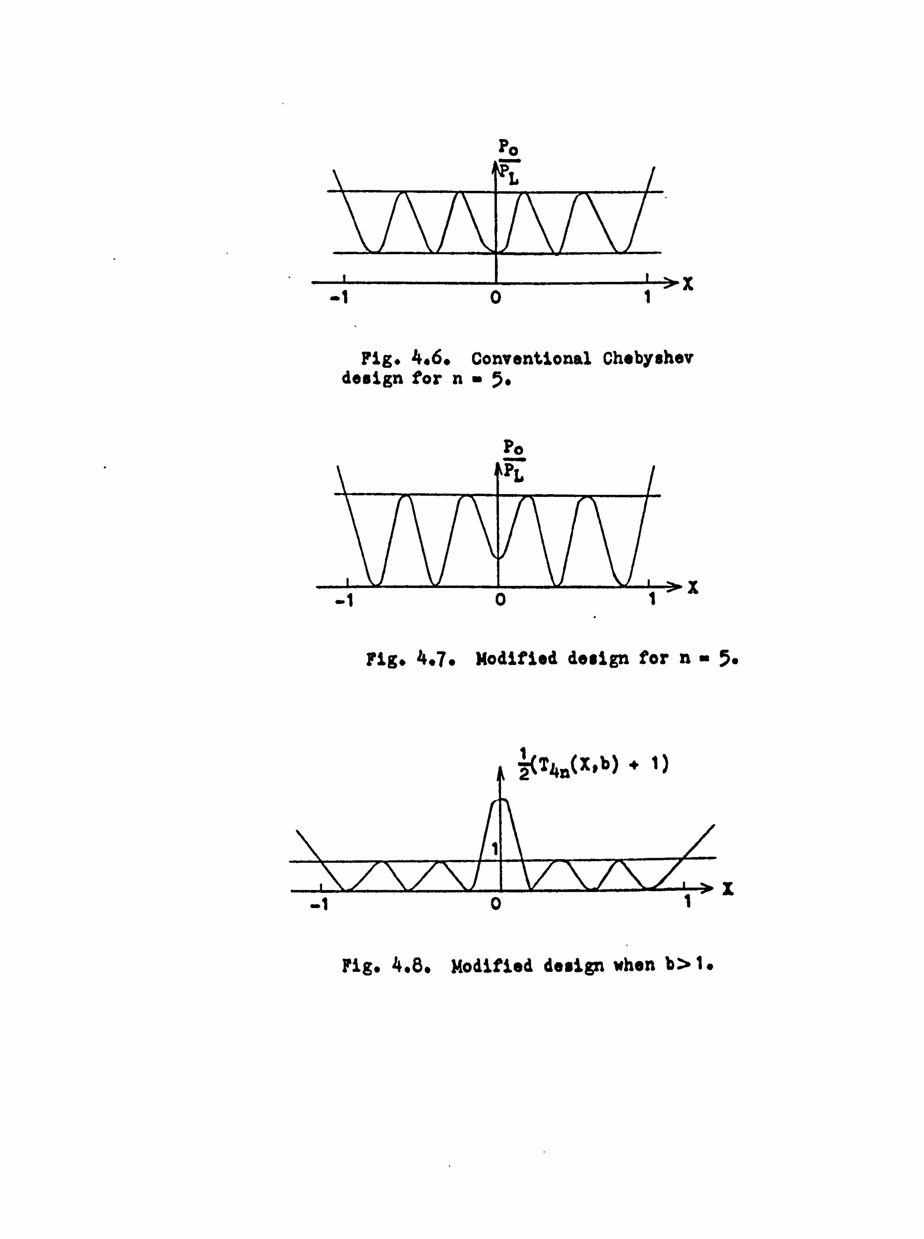
pa
X
Fig. 4.6. Conventional Chebyshev design for n"5.
Pa
X
Fig. 4.7. Modified design for n"5.
1T. : Y_1%% a 11
I
Fig. 4.8. Modified design when b> 1.
-i o1
_1 v
o1 -1
91
where
ell te (R-1)2 + e2 4R
In the appendix it is proved that Eq. (4.43) has a
faster rate of cutoff in the attenuation band than any other
polynomial specification, including Eq. (4.42).
There is an interesting comparison between Egs. (4.42).
and (4.43). In Eq. (4.42) the zeros of r (s) i'(-s), which p,
are the factors of p -1, are not on the imaginary axis but L
have both real and imaginary parts. As discussed in chapter
2, this fact means that there are many different choices
available for the zeros of r(s), with the number of choices
increasing rapidly with n. In a specification of the type
of Eq. (4.43), however, it is'seen that all except two of the P
zeros of P° -1 are double and on the imaginary axis. The
L
other two zeros are on the positive and negative real axis
and equidistant from the origin. This means that there will
be only two choices available for the zeros of r(s).
In the design of even order filters the function
L4n(X, b) has an interesting property. When b> 1, the
argument 2n coe-1( [1+b] X2-b) becomes pure imaginary as X8 0, resulting in J [T4(x, b)+] having the shape
depicted in Fig. 4.8. This characteristic may either be
used in the design of low-pass or band-pass filters. It

92
is equivalent to a function previously described by
Matthaei(14).
There is-still much interesting work to be done with
the L2n(X9b)function described previously. It would be very
rewarding to find closed formulae for the element values in
a lumped filter those insertion loss is described by
p®_ 1+ e2
IL2(X, b)± 1. These element values would be
2
functions of eta b, and n. When ba 19 the element values so
determined must agree with Takahasi's results(4), which use
"pure" Chebyshev polynomials (Tn(X)) in the insertion lose
description. Some preliminary work on this problem has
already been done. It has been found that whereas the poles
of r (s)(7 ca) lie on an ellipse for the "pure" Chebyshev
case, they do not lie on an ellipse for the L2n(X, b) case
when bf1. A good discussion of Takahasi°s proof, which is
very suggestive and contains useful information for dealing
with the above problem, is given in Weinberg's book(3). An-
other useful project would be the compilation of tables to
"fill in the blanks" in Weinberg's tables of Chebyshev filters(3)
for the cases where n is even and R 1. Also, if only R. n,
and the maximum paseband insertion loss are specified, it was
previously seen (Figs-4.6 and 4.7) how the conventional in-
sertion loss can be improved in the stopband. A set of tables
for this case would be worthwhile.

93
4.5 Proof That the Ln Polynomials Are Optimal.
It was stated earlier that, of all polynomials of degree
2n required to be bounded in magnitude by unity in the pass-
band -1. X1 and required to have a given absolute value be-
tween 0 and 1 at X- 0, the polynomial which exceeds all others
in the. stopband IXI' 1 is L2n(X, b), which is defined through
Egs. (4.17), (4.18), and (4.19). The proof of this statement
is shown in two steps.
First, assume (LOCI > 0. L6(W, b) would then have the
shape shown in Fig. 4.9, for example. Now let there exist
another polynomial of degree 2n, P2n(X), which satisfies the
above passband conditions, and in addition has the property IP2n(Xo)l >f Xo )l (4.44)
at least at one point X0 in the stopband interval.
The polynomial
Q(X) L2n(X, b) - L2n(Xp, b) . F(X) (4-45)
P2n(Xo) ýn
has 2n zeros in the passband -1 X 1. To see this fact,
refer to 'Fig-4.9- IL2n(O, b)J ý [?
2n(O)frICI , where point. C
is shown in the Figure. Thus L2n(Xo, b) $ (0) dAI 4 ICI, and
2n p2n(Xo)
hence point A is "trapped" inside the curve DCE. As X varies
from O-VI 1, L2n(Xo, b) g2n(X) must intersect Ln(X, b)
P2n(Xo )

rY_til
z
Fig. 4.9. Demonstration of the optimal property of Ln(X, b).

94
n times, giving rise to 2n zeros of Q(X) in the passband.
But Q(X) also has a zero at X0, which means that Q (X) is
at least of (2n+ 1) degree, which is impossible, since by
construction it is of degree 2n. Thus Eq. (4.44) is false,
and L2n(X, b) must be the optimal polynomial.
Next consider the case where LDC -- 0. Q(X) is again
constructed as in Eq. (4.45). Similar to the above method,
it is readily seen that Q (X) will have 2n-2 zeros on the
range 0< IXk 'ý' 1. Since P2n(0) = L2n(0, b) u 0, Q, (X) will have
at least one more zero at Xn 0. Now at X-+, l, Eq. (4.17)
gives
L2n( t l, b) ä cos(n cos-l(1))
ýM. cos Od1. (4-46)
But L2n(Xo, b) 2n(1) <1 and so Q(X) will be positive
P2n(Xo)
at X- ±1. Since the sign of Q(X) is the same at each end
of the interval C 1,1. ], it must possess an even number of
real zeros within this interval. Hence the degree of Q(X)
is at least 2n. In addition Q (X) also has a zero at X0,
and is therefore of 2n+ 1 degree. But by construction Q(X)
is of degree 2n, and therefore Eq. (4.44) is false, and
L2n(X, b) must be the optimal polynomial.
It is seen that for the above proof to hold, it is
necessary for point C to be of opposite sign to D and E.

95
In Eq. (4.17) it is therefore necessary for e to be in X=0
the interval nW - IT, nil . This is automatically insured 2
by Egs. (4.18) and (4.19).
96
Chapter 4 REFERENCES
1. Papoulis, A.: "On the approximation problem in filter
design", IRE National Convention Record, Part 2,
1957, Pp. 182-183-
2. Levy, R.: "Tables of element values for the distributed
low-pass prototype filter", IEEE Trans. MTT,
Vol. MTT-13,1965, pp" 514-536. 3. Weinberg, L.: "Network Analysis and Synthesis".
McGraw-Hill, Inc., 1962, Chapter 13-
4. Takahasi, H.: "On the ladder-type filter network with
Tchebysheff response", J. Inst. Elec. Commun. Engrs.
Japan, February, 1951, Vol. 34, No. 2 (in Japanese).
5. Lind, L. F.: "Synthesis of equally terminated, low-pass,
lumped and distributed filters of even order",
IEEE Trans. MTT (to be published).
6. Jones, N. B.: "Lowpass filters with approximately equal-
ripple modulus error", Electronics Letters, 1967,
Vol. 3, PP- 516-517. 7. Jones, N. B. and Wood, R. A.: "Generalized Chebyshev lowpass
filters", Electronics Letters, Vol. 4,1968,
PP. 158-159.
97
Chapter 4 REFERENCES (continued)
8. Vasil'yev, V. B.:. "Optimum microwave filters with an
even number of sections". Telecommunications and
Radio Engineering, August, 1966, Vol. 21, No. 8,
pp. 85-91. (English edition of Russian Technical
journals Elektrosvyaz' and Radiotekhnika. )
9. Weinberg, L.: - "Network Analysis and Synthesis".
McGraw-Hill, Inc., 1962, pp. 512-513-
10. Weinberg, L.: "Network Analysis and Synthesis".
McGraw-Hill, Inc., 1962, PP- 595-597-
11. Bingham, J. A. C.: "A new method of solving the accuracy
problem in filter design", IEEE Trans., Sept. 1964,
CT-1l, PP. 327-341.
12. Saad, T. S.: "Microwave Engineers Technical and Buyers
Guide Edition, 1968". Horizon House, p. 44.
13. Levy, R. and Rozzi, T.: "Precise design of coaxial
low-pass filters", IEEE Trans. MTT, Vol. MTT-16,
March, 1968, pp. 142-147.
14. Matthaei, G. L.: "Tables of Chebyshev impedance-transform-
ing networks of low-pass filter form", Proc. IEEE,
1964, Vol. 52, No. 8, pp. 939-963"

98
Chapter 5. Branch-Guide Directional Couplers.
5.1 General Directional Coupler Theory(l)
5.1.1 The Scattering Matrix.
In chapter 2 it was shown that the scattering matrix
for a lossless, reciprocal network has the properties: .. 1 1) Sjj - Sjj, or 8=8, (5.1)
i. e., the scattering matrix and its transpose are identical.
Also, the scattering matrix is unitary, or
2) (S)(s)= in" (5.2)
From these two properties, 'it is easily seen that
(s)(S ). ln, (5.3)
where * indicates complex conjugate, and In is the unit matrix.
It was also shown that the scattering matrix always exists
for a passive network.
Consider now a lossless, reciprocal 4-port network
having a specified load impedance at each port. The net-
work is defined to be a directional coupler 'if, at some
center frequency, its input ports can be grouped into two
pairs having the following properties:
1) Each pair of ports is mutually isolated, (5.4)
2) The ports of one pair are both matched. (5.5)
The 4-port network is shown in Fig. 5.1, where ports 1,2
and 3,4 are the mutually isolated pairs. In this coupler
port 1 delivers coupled power to port 3, and port 2 delivers
coupled power to port 4. Coupling between ports j and k is
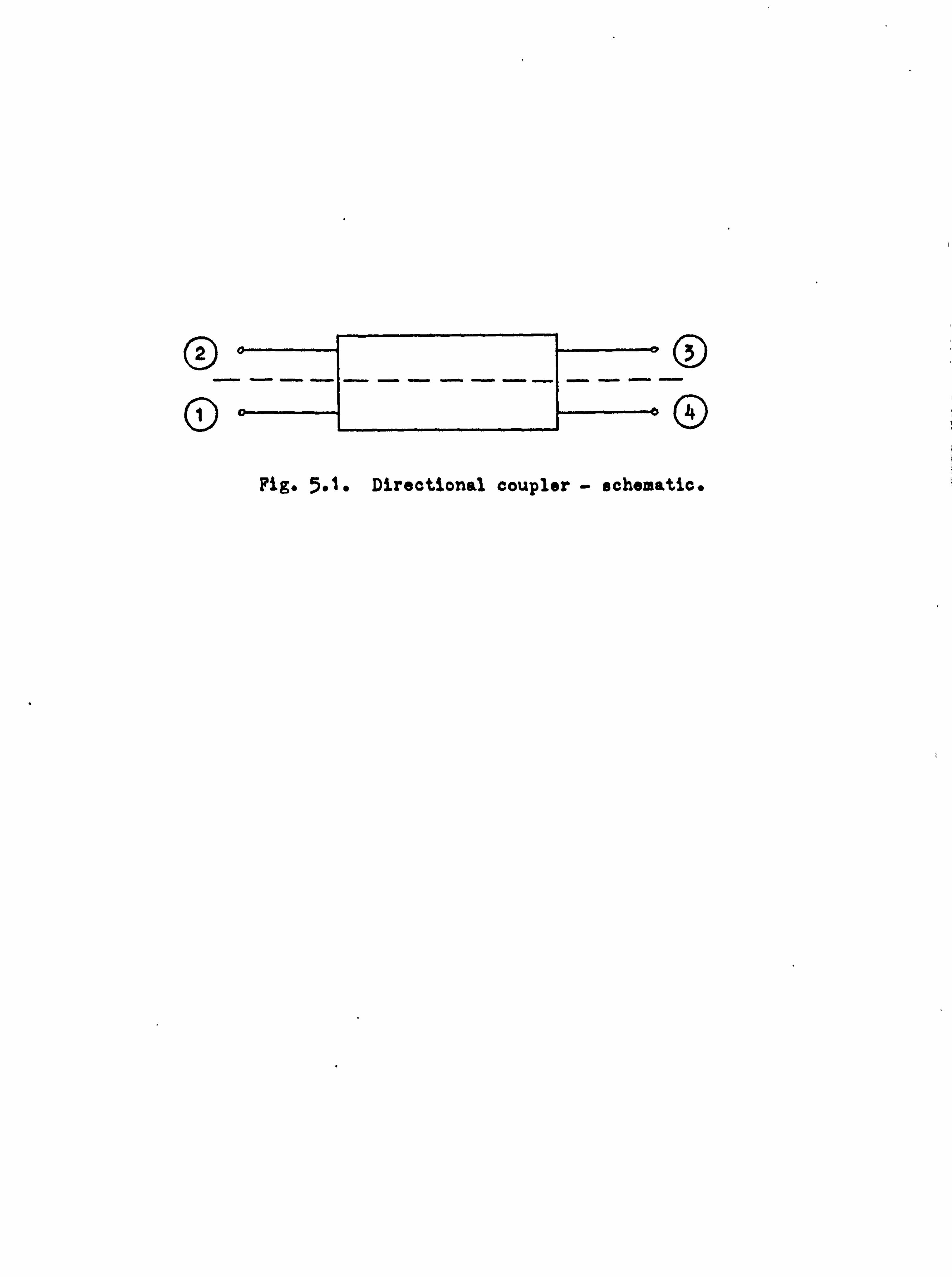
00 00
Fig. 5.1. Directional coupler - schematic.
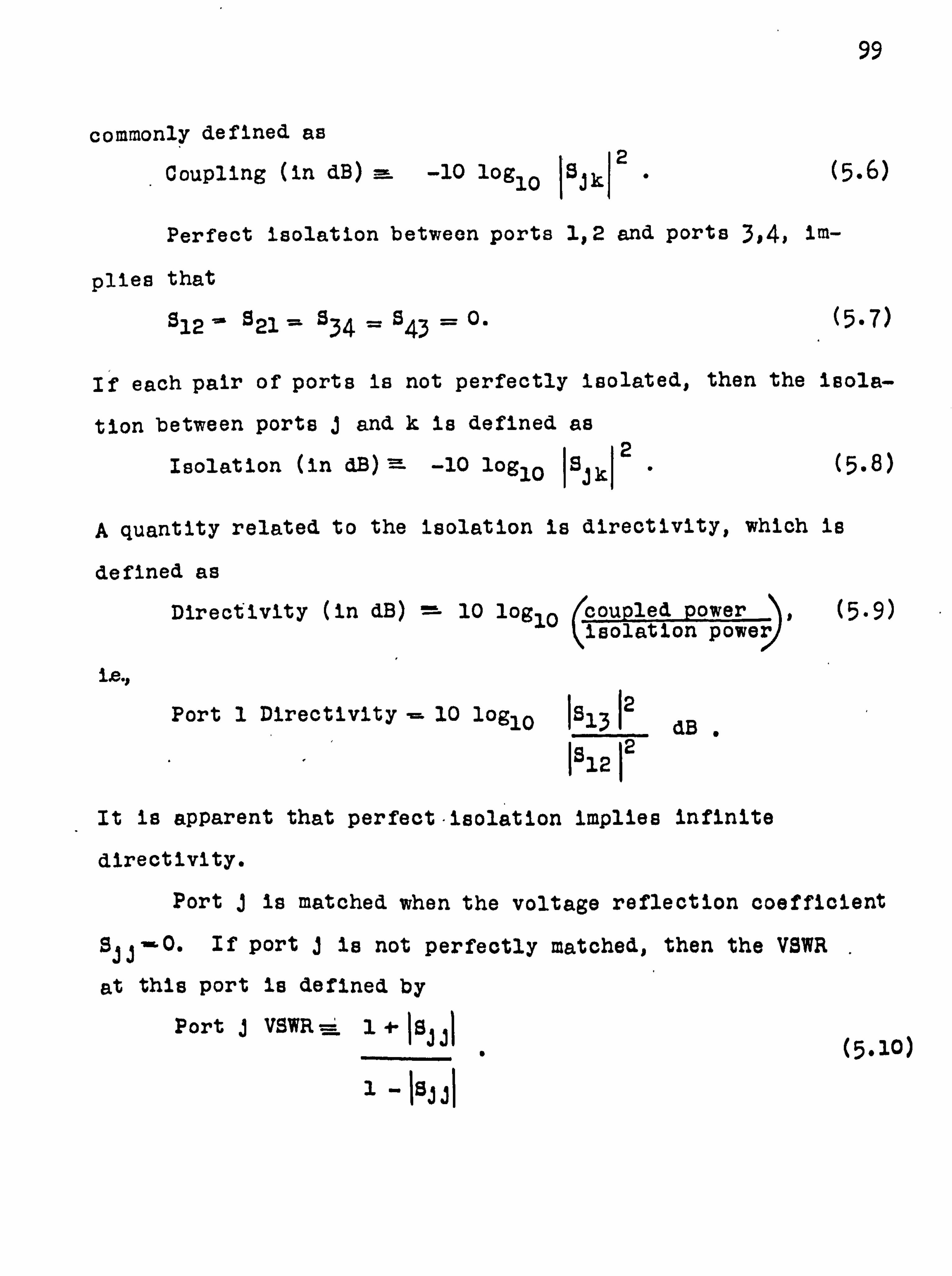
99
commonly defined as
Coupling (in dB) m -10 log10 Isjk2 .
(5.6)
Perfect isolation between ports 1,2 and ports 3,4, im-
plies that
s12 ' '921 = 534 = 543 = o. (5.7)
If each pair of ports is not perfectly isolated, then the isola-
tion between ports j and k is defined as 2
Isolation (in dB) = -10 log10 I8jk1 .
(5.8)
A quantity related to the isolation is directivity, which is
defined as
Directivity (in dB) = 10 log10 coupled power , isolation power
is.,
Port 1 Directivity - 10 log10 161312 dB
IS12 I2
It is apparent that perfect-isolation implies infinite
directivity.
(5.9)
Port j is matched when the voltage reflection coefficient
8j i=0. If port j is not perfectly matched, then the VSWR
at this port is defined by
Port j MR-Ei 1 18A (5.10)
1'IsiJI
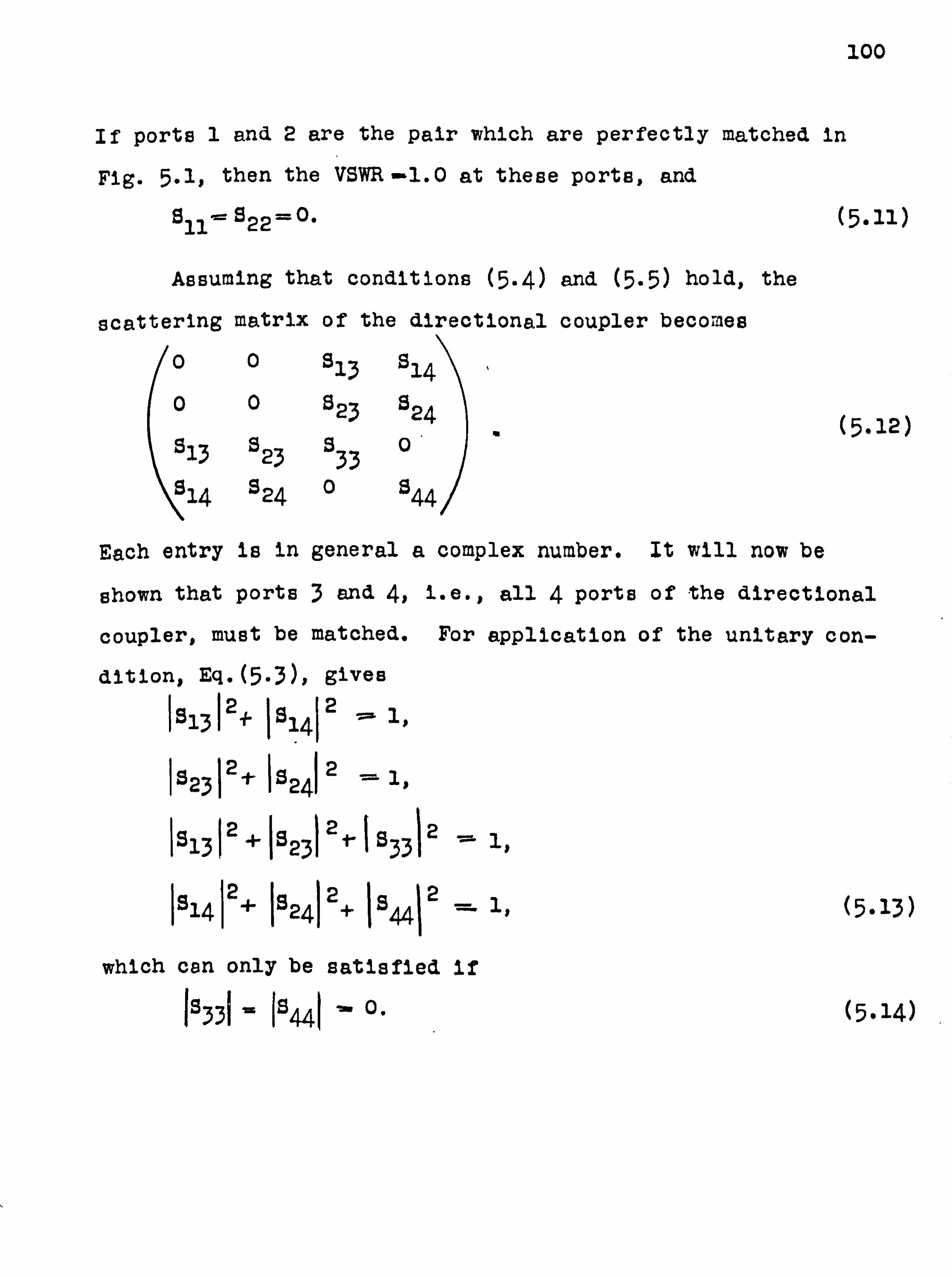
100
If ports 1 and 2 are the pair which are perfectly matched in
Fig. 5.1, then the VSWR -"1.0 at these ports, and
0 11_ 022 = o. (5.11)
Assuming that conditions (5.4) and (5.5) hold, the
scattering matrix
00
10 0
513 523 \514 S24
of
S3
S23 533
0
the directional coupler becomes
14 s24
(5.12) 0
$44
Each entry is in general a complex number. It will now be
shown that ports 3 and 4, i. e., all 4 ports of the directional
coupler, must be matched. For application of the unitary con-
dition, Eq. (5.3), gives
I s13 12+ 1s12 .1,
Is23I2Is24I2 1'
I1,
161412+ Is2412+ I s44 2=1, (5-13)
which can only be satisfied if
1'9330 a IS441 ' 0' (5-14)
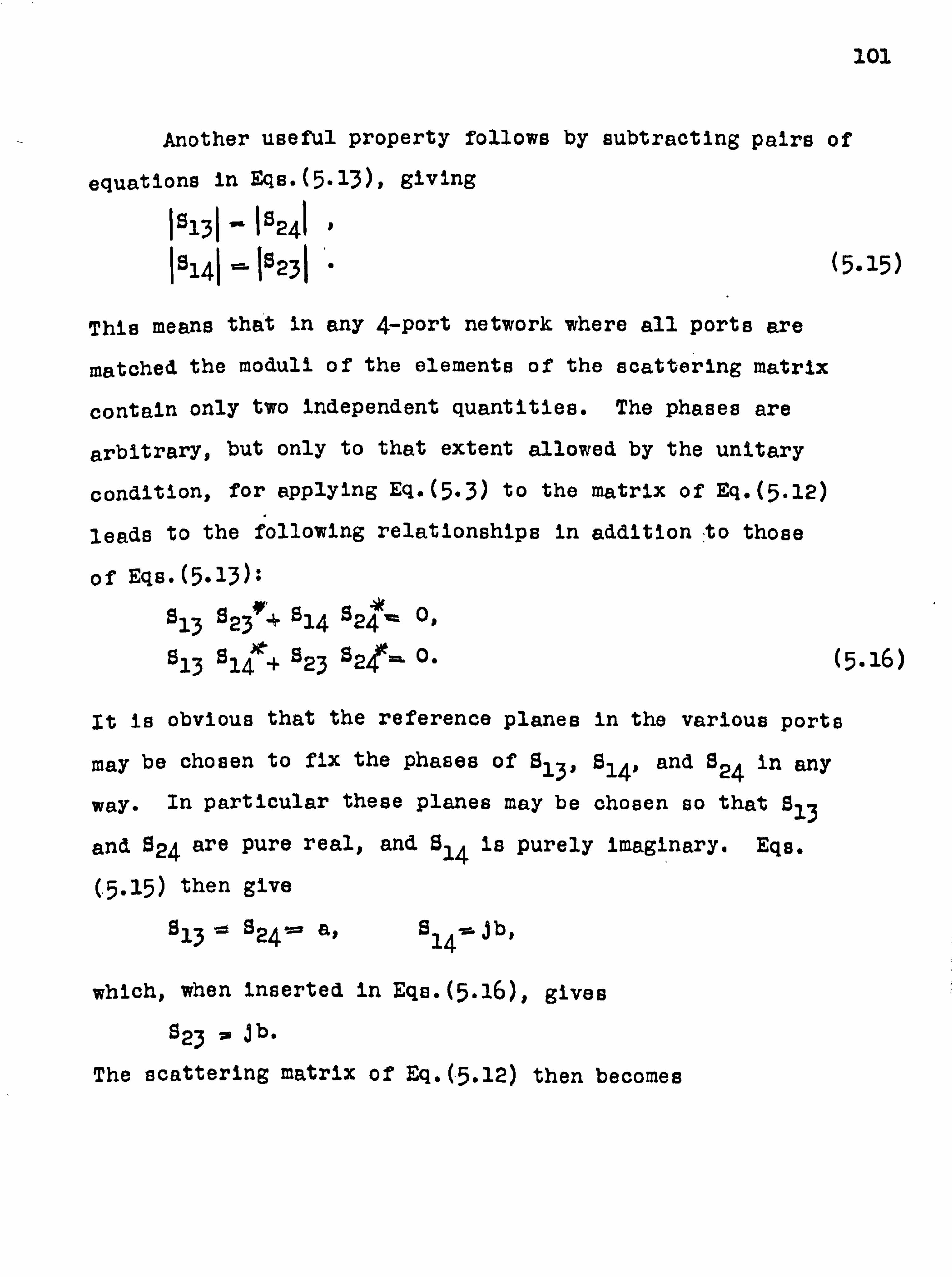
101
Another useful property follows by subtracting pairs of
equations in Egs. (5.13), giving
I8131 Is241
I '4l 123I . (5.15)
This means that in any 4-port network where all ports are
matched the moduli of the elements of the scattering matrix
contain only two independent quantities. The phases are
arbitrary, but only to that extent allowed by the unitary
condition, for applying Eq. (5.3) to the matrix of Eq. (5.12)
leads to the following relationships in addition to those
of Eqs. (5.13):
s13 S23 ̀ : + s14 24 ' 0,
s13 s14 + g23 82(= 0. (5-16)
it is obvious that the reference planes in the various ports
may be chosen to fix the phases of S13, S141 and S24 in any
way. In particular these planes may be chosen so that 813
and S24 are pure real, and S14 is purely imaginary. Eqs.
(5.15) then give
S13 S24' a, 914= j b,
which, when inserted in Egs. (5.16), gives
S23 = jb.
The scattering matrix of Eq. (5.12) then becomes

102
00a ib
to 0 jb a II" (5.17)
a jb 00
,ba00
Hence, by proper location of the reference planes, the scat-
tering matrix will contain only two arbitrary quantities.
It has been shown that all directional couplers are
perfectly matched, and by applying similar methods to those
above it is easily proved that the converse is true, that
all 4-port junctions which are perfectly matched are direc-
tional couplers.
5.1.2 The Symmetric Directional Coupler.
One of the most common and useful classes of directional
couplers is completely symmetric, i. e., one where ports 1,2,
3, and 4 of the coupler in Fig. 5.1 are physically indistin-
guishable. Assuming that the coupler is slightly imperfect
(that there is finite isolation and slight mismatch, although
symmetry is still preserved) then the scattering matrix is
restricted by the symmetry properties as follows:
Sll' s22-03.3 844 S12 = S21= 834- 843
s31. e24=e42 S13- '. s14= 841=523'832
, (5.18)

103
so that the scattering matrix becomes
s11 X12 913 214
s12 s11 l4 13 (5.19) S13 g14 sll X12
X14 S13 B12 911
and the unitary relationship, Eq. (5.3), gives the following
four equations:
ll(2 +8 12I2 .' 1813 2
+. 1ß14I2
= 1D
1911912 ý° s12g11 + '913514 + g14S13 =i °D
x11213 + $12s1, e + s13S1lt+- s]. 4812'ß _ 0,
ol1814 31231.3 4+ '913S1 + '91481i 0. (5.20 )
From these equations it is possible to work out some useful
general properties of the symmetrical coupler, particularly
the phase difference between the waves coupled from port
1 to ports 3 and 4. The last two of Eqs. (5.20) may be
rearranged to form the product
41 (511s13 s12$]1) (albs14 + sl* s13 )
(s13sll + S10124)(512gi3 + S14 811), (5.21)
which reduces to
( IS111 2-L1 2) (913 814 - s13814 )
(81312 -
IS1412) (811! 812 - 811812 )" (5.22)

104
If for the present the condition for perfect isolation between
ports 1 and 2 is introduced, i. e., that S12 w O,, Egs. (5.20)
and (5.22) reduce to:
Isý1+1131+'1814)2.
g13B14 4- 514313#
s11s13 + g135ii = o,
1311s14 514611 o,
8111 2(s13s14-s13s14)'-- 0. (5.23)
Equations (5.23) can be satisfied simultaneously only if
gil ` 0, for if 8110 0 then either 813 or S14 must vanish,
resulting in degenerate cases of no interest. This means
that in a symmetric coupler, perfect isolation, 812=0, implies
perfect match, Sll* 0. Equations (5.23) then reduce still
further as follows
IS131 2 +. L14 12 1" (5.24)
S13814 . S145133- 0 (5.25)
The phase relationship follows from Eq. (5.25), for putting
1l4I eJe4 this becomes S13-' ll3I e, ®3 and 5141 ,
cos (A3- 04) = o, (5.26)
105
co that for perfect match and isolation, the symmetric direc-
tional coupler posseeses a 90° phase difference between the
waves in the two output arms.
5.1.3 The Symmetric Hybrid Junction.
A case of particular interest is that of the 3-dB
coupler, that is, one giving equal power division between ports
3 and 4. The symmetric 3-dB coupler is, in fact, a hybrid
junction. It may be realized in many forms, e. g., in rectan-
gular waveguide as the short-shot (narrow-wall) coupler, the
top-wall coupler, and the branch-guide coupler. In quasi-
optical guide wave systems it appears as the semireflecting
mirror or as a quarter-wave plate ; or in TEM-line systems
as the coupled transmission line (proximity) 3-dB coupler,
or as a branch-line coupler. The branch-line and branch-
guide systems are described in greater detail in subsequent
sections of this chapter. At this stage, however, it is con-
venient to derive properties common to all symmetric 3-dB
couplers whatever their physical form. It has already been
shown that a perfect symmetric coupler, 3-DH or otherwise,
gives a quadrature phase relationship between the waves in
the two output ports. It is of interest to find the phase
relationship of a slightly imperfect 3-dB coupler, i. e.,
one with finite isolation and slight mismatch. This gives
information about the bandwidth properties of the 3-dB coupler
when used as a hybrid.

lob
Eq. (5.22) may be written in terms of the moduli IS lki
and arguments E) k of the Slk parameters (k= 1,2,3,4) to give
(ISlll 2 -1812
12) I' 15141 sin(e3 -194)
(P13I2 -I Sl, 2) Islll "( ßl21 sin(e1 - e2). (5.27)
In the case of a slightly imperfect hybrid,
IS13I -- ISi4c2i
,
(e3 - 94)= 2,
Isii1 0 512, Gt 10
whence Eq. (5.27) reduces to
ISul 2- 1s1212
2(IS13I 2- Is14I2) 1 sll1 " 1'9121 sin(E - E)2),
which, by virtue of Eq. (5.28), is very small (i. e., at
least an order of magnitude less than either jSlA 2 or
Is12I2), leading to the final result that Iý
11I S 12 II
Eq. (5.32) states that the magnitude of the reflected wave
at the input port is equal to that of the wave appearing
from the "isolated" port, implying the relationship be-
tween the input VSWR and the isolation of the hybrid as
(5.28)
(5.29)
(5.30)
(5.31)
(5.32)
shown in Fig-5.2. The experimentally determined performance

N d d
u
e 0 ö
d M W a 0 t a
1
l
,
1 1
i i
4
0 10 20 30 40 by Isolation (db)
I. 4
1.3
1.2
i t t t t
3 II vi >
60
Fig. 5.2. Theoretical phase deviation (-) and VSWR (- -) of an imperfect symmetric 3-dB coupler.
107
of many symmetric hybrids show that this relationship holds
quite closely. An analysis of a branch-guide hybrid yielded
the points shown the Figure, showing again the correctness
of the approximate equality of Eq. (5.32). Symmetry con-
siderations (i. e., the 3-dB coupling) make this conclusion
seem entirely reasonable.
Another useful result is obtained by writing the second
of Egs. (5.20) in the form ISiil
' iS]. 2L cos (®1 - ®2) -h1ß131 I Slý coa (193 - ®4) wý' 0,
giving Icos(93
- ®4)I = 18111 ° tsi21
IC08091 - 82)a (5.33)
12131 ° 16141
which, using Egs. (5.28) and (5.32) gives in the worst pos-
sible case (when O 1= ) the relationship
Lcos (03 - 94)I 21 5121 2
= 2(10-1/10)0 (5.34) where I is the isolation of the hybrid (in dB) when port 1
is the input port. Thus when the isolation is 30dB,
Ccos(63 - ®4)I= 2x 10 3,
giving a phase difference which
differs from the ideal 900 by only 0.1°. When the isolation
has fallen-to 20dB, the phase difference has increased to 1.20.
The complete form of Eq. (. 5.32) is shown in Fig-5.2. Since

108
3-dB couplers with values of isolation over a broad band of
25 dB or even of 30 dB are quite common, Fig-5.2 shows that
the phase deviation property of these devices is extremely
good, and equally broad band. Thus, it is possible to con-
struct phase-measuring bridges incorporating 3-dB hybrids
which give high accuracy over broad bandwidths. A further
result is that when dealing with applications of the hybrid
where the output arms may be short-circuited, as in a duplexer
or diplexer, it is usually not necessary to take the phase
variation into account as it is so small.
5.1.4 Directional Coupler Even and Odd Mode Analysis.
By the adoption of the scattering matrix for the des-
cription of a multiport junction, the problem of the solution
of Maxwell's equations for the boundary conditions inside the
junction has been deliberately relinquished. This is neces-
sary for most practical junctions because of the usually in-
surmountable mathematical difficulties encountered. The
symmetry of the junction can, however, provide some knowledge
about the field in the interior. Thus, suppose the direc-
tional coupler depicted in Fig. 5.1 has a symmetry plane as indicated by the dotted line. Then if two signals of
amplitude j and in phase are applied to ports 1 and 2, by
symmetry a voltage maximum occurs at every point on the
line of symmetry. On the symmetry plane then Z -oo, i. e.,
1o9
the junction may be open-circuited at the plane without affec-
ting the field distribution, or alternatively a "magnetic wall"
may be located at this plane (Fig-5.3a). Similarly, if two
signals of amplitude . and out of phase are applied to pörts
1 and 2, a voltage minimum occurs on the line of symmetry.
On the symmetry plane Z$0, i. e., a short circuit (an "elec
tric wall") may be located at the plane without affecting the
field distributions, as shown in Fig-5.3b. These two modes
of operation of the junction are called the even and odd
modes, respectively. They are the so-3alled normal modes
of the junction. For each normal mode, the problem reduces
to that of a 2-port network, for which a solution may generally
be obtained. By superposition, the sum of the two normal mode
field distributions corresponds to that given by a signal of
unit amplitude input at port 1. The resultant signals out
of each port are also given by the superposition of those
obtained in the even and odd modes. For the even mode a
reflection coefficient re=s lleven and a transmission
coefficient Te 812 even are determined, and similarly for
the odd mode, roa 8ll odd and To = 812 odd are determined.
Superposition gives the following vector amplitudes of the
signals emerging from the 4 ports: b1=+ßr'6 +("0), b3 =4(Te - To»,
(5.35) b2=4(re - ro), b4=3(Te + T0).
H- Wal l
IIE roe To*
0 0 (c)
9- Wall
roe To. r.. 0
(b)
Fig. 5.3. (a) Even mode excitation and (b) odd mode excitation.
110
In chapter 2 it was found that the reflection coefficient r'
for a lossless network having a transfer matrix A DB )p an CC D
input source resistance R, = 1 ohm, and a load resistance
RL (normalized to Rs), is given by
(A - OLD) + (GLB -C) (5.36) (A+ GLD) +(GLB*C)
where GL-= 1/RL. For this network the associated trans-
mission coefficient T- S12 can easily be shown to be(2)
zý2f G-L "
(5.37)
(A +GLD) + (cLB 4-C)
The analysis of the two networks for the even and odd
modes is frequently possible, whence Egs. (5.36) and (5.37)
are then used in conjunction with Eq. (5.35) to determine
the four port behaviour of the coupler. An additional
relationship between r and T for a two port network can be
derived through use of the unitary condition, Eq. (5.3).
This relationship is
Irl2+ IT12 1. (5.38) In words, this equation states that the sum of the trans-
mitted power plus the reflected power equals the incident
power. This must be true, since a lossless network cannot
absorb power.
111
The above discussion of the various properties of direc-
tional couplers is general and is found to apply to many differ-
ent types of couplers. The discussion, will be become more spe-
cialized and will deal exclusively with branch-guide directional
couplers.
5.2 Development of Symmetric Branch-Guide Directional Couplers.
5.2.1 Basic Description.
Branch-guide couplers may be constructed using many types of
waveguides. or transmission lines. In the branch-guide coupler
using rectangular waveguides, the coupling region consists of a
number of series branch-guides, eachigo/4 in length at the mid-
band frequency, connecting the two waveguides. These branch
guides are themselves spaced at Intervals of )go/4, as shown in
Fig. 5.4. To obtain an optimum broadband performance it is nec-
essary to specify the impedances of both the branch guides and
the connecting or main line waveguide sections, as will be shown
later. In the case of TEM-mode transmission lines, the branch
lines are in shunt rather than in series with the main lines,
representing the dual .f the waveguide case.
Some of the properties of branch-guide couplers which
make them particularly useful in several applications have
been summarized by Young(3). Probably the most significant
are as follows:
1) The coupling between the two lines is through join-
ing branch-lines of finite length, and not through apertures.
This gives additional flexibility in design; e. g.,

90
0 11r.
go/4
OO
Fig. 5.4. Cross section of a multibranch waveguide coupler.

112
special-purpose chokes or filters can'be placed in the
branches.
2) The coupler is better suited for strong coupling
('stronger than 20 dB) than weak coupling; 0-dB couplers are
feasible over large bandwidths.
3) In waveguide, the coupler E-plane cross-section
is constant. It can therefore be milled in two blocks and
assembled by the "split-block" construction. Other components
can also be milled into the same block.
4) Branch-guide couplers are capable of handling high
RF powers.
5.2.2 Analysis of the Branch-Guide Couple r. (4)
The analysis of the coupler is in terms of the even and
odd modes, as described in section 5.1.4. The plane of sym-
metry between the two waveguides bisects the branch guides
transversely. The even-mode 2-port circuit comprises a num-
ber of open-circuited stubs,, and the-odd-mode 2-port circuit
a number of short-circuited stubs, connected to the main
waveguide. At the midband frequency the branch stubs will
be Ago/8 (6=45°) long, and spaced by A g0/4 (6,, 90°) along
the main waveguide. The transfer matrices for the lossless
even and odd mode configurations are obtained by multiplica-
tion of the individual matrices of the open or short-circuited
stubs, and connecting line sections. The values of re end

113
Te, ro and To are obtained by application of Egs. (5.36) and
(5.37) to the appropriate matrices, and the values of-the
wave amplitudes and phases emerging from the four arms are
given by Eq. (5.35).
5.2.3 Early Developments.
The earlier papers(4) on branch-guide couplers concen-
trated on the development of the above even and odd mode
analysis, and no attempts at a synthesis technique were des-
cribed. The assumption normally made in these designs was
that the main line impedances were not varied, i. e., they
were all equal to the characteristic impedance of the out-
put and input lines of the coupler. Then the design problem
was to find a suitable "taper" for the characteristic im-
pedances of the branch lines. Multibranch couplers with
tapered branch line impedances were in use during the ee. rly
1950's, and the first paper on a binomially taper was pub-
lished by Lomer and Crompton(5). The extension to give-a
Chebyshev distribution was described by Levy(6), and a
marked improvement in match and isolation over a specified
bandwidth resulted. In both of these methods the stub im-
pedances are made proportional to the desired impedance
taper at midband. Then the structure is analyzed (by the
even and odd mode method described above) and the constant
of proportionality is determined by the center frequency
114
coupling requirement. Having established the branch line
impedance values, the coupler performance over a band of
frequencies is found by repetitive analysis. The main line
sections may be included in this analysis. This technique
is very empirical, i. e., it is difficult to predict what
the frequency band performance of a given taper will be.
5.2.4 Patterson's Theory(7).
As in the previous designs, this theory assumes that
the main line impedances are all equal to those of the input
and output lines. These connecting lines are now regarded
as impedance inverters at midband, as they are a quarter
wavelength long at this frequency. It is assumed that over a
narrow frequency band (centered at midband) the main lines will
remain frequency invariant, and thus continue to act as ideal
transformers. Therefore it is possible to draw an equivalence
between the even and odd mode 2-port networks and prototype
high- or low-pass lumped-element networks, as shown in Fig. 5.5"
The element values in the lumped low-pass network of Fig. 5.5b
are chosen to give either a maximally flat insertion loss
(as discussed in chapter 2) or a Chebyshev insertion loss
characteristic (as discussed in chapter 4). Then the net-
work in Fig-5.5a will have a corresponding high-pass inser-
tion loss characteristic.

H-wall _ ýýz
11 ZO "1 ZO -1
gn/s gu/s g3/5
g2/s 1
(a) Even Mode E-wall 81e 8a- gns
Z1 Z2 Zn 1 4-L T 92e 1
Zo -1_ zo .1
(b) Odd Mode
Fig. 5.5. Equivalent circuit representations for even and odd modes in Patterson's Theoryt (a) even mode and (b) odd mode.

115
The equivalence between the distributed and lumped
elementsis given by making the respective branch line
series reactances proportional to those of the prototype
filter network. The constant of proportionality is deter-
mined by analysis and the center frequency coupling require-
ment. All branch line reactances are multiplied by this
constant. This has the effect of replacing s by tan ® in tan o
the low-pass network, as discussed in chapter 3. In a five
branch maximally flat 3-dB coupler, for example, t&n 6°w 2.08,
or E) 0=
63.4. Superposition of the high-pass and low-pass
networks (Eq. 5.35) gives the "Passband" of the coupler as
going from() 1= 26.6° to e2= 63.4°. The assumption that
the main connecting lines act as ideal transformers (900 in
length) over the above passband is a very serious one indeed.
Still, this theory gives good results in practice(7). Also,
an attempt has been made to incorporate the frequency be-
haviour of the branch lines into the design procedure.
. 2.5 Young's Theory (4).
In Patterson's design method , the main line impedance
Is usually maintained uniformly throughout the coupling
region. An approach which requires this impedance to vary
between the branch guides has been described by Young(3).
In this approach, the coupler is derived from a prototype
116
quarter-wave transformer, tables of which have been pub-
lished (8).
The first step is to choose a suitable quarter-
wave transformer prototype having a known bandwidth, passband
performance, and output to input resistance ratio R. Usually
either a maximally flat or Chebyshev passband characteristic
is used. Then the VSWR at each junction of this prototype is
calculated, using the relation VS1ºR
Q 1*
_,
(5e10/
l-1ri where
Z BZ A(5.39)
ZB+ZA
and ZA and ZB are the impedances to the left and right of the
junction, respectively. The next step is to equate these
junction VSWR's to the junction VSWR's of the even (or odd)
mode circuit for the coupler. A typical junction is depicted
in Fig-5.6. The admittance value for the, stub in the even
mode circuit is -jY, and for the odd mode circuit is + jY.
For either circuit the junction VSWR in Fig. 5.6 may be cal-
culated with the help of Egs. (5.10) and (5.39) as S
VS WR (Kl 4' K2)2 +. Y2)j + ((Kl-K2)2,,, Y2)j ( 54o) ý(Kl -K2)2+Y2)' -((Kl-K2)24. Y2)'
where K1 and K2 are admittances in Fig. 5.6.

circuit stub
Input )utput
Fig. 5.6. Equivalent circuit of a shunt stub in an even or odd mode excitation.
v- JUnCI10f1 V. . W. K

117
An important difference between the equivalent circuit
of this junction and that in the prototype is that whereas
in the latter the junction discontinuity is purely resistive,
in the case of the coupler the discontinuity represented by
the stub is mainly susceptive or reactive. It is necessary
to adjust the distance between the junctions to allow for
this effect, i. e., to first establish reference planes on
either side of the Junction where the reflection coefficient
is pure real, and then to have adjacent reference planes
touch while keeping the distances between junctions at 900
(electrical length) at midband. This is called the synchro-
nous-tuning condition by Young(3). In Fig-5.6 it is easily
found that
tan-1 2YK1
Y2+ K22-K12
02 ý 3. tan" 2YK2
Y2+ Kl2-K22
At each junction only the ratio of impedances is im-
(5.41)
portent, and so only two and not three quantities have to be
solved for. All of the coupler impedances may be normalized
to the input and output system impedances at the end of the
design procedure, if desired. But at each junction the two
118
equations (5.40) and (5.41) are available, and thus the
element values in the coupler may be found. In order to
apply the synchronous-tuning condition at all steps in the
design, the first step is to solve for the junction (s) at
which the electrical length is known by symmetry considera-
tions, i. e., in the middle of the symmetrical coupler. - Then
one "works out" from the center of the coupler until all im-
pedances have been determined. Special design charts have been
prepared by Young to facilitate this procedure.
Knowing the coupler specifications of bandwidth, pass-
band VSWR amplitude and shape, (i. e., maximally flat or Cheby-
shev), and center frequency coupling level, a suitable low-
pass quarter-wave transformer prototype may be selected as
follows. Young has empirically given a bandwidth contraction
factor B. which results in equivalent VSWR's for the two
structures, i. e.,
B= Bandwidth of coupler Bandwidth of transformer
B is found to vary between .5 and . 7, and is presented in
graphical form in the original paper(3) for a variety of
cases. Young has also found that when the coupler is matched
at center frequency, then the coupling is related to the out-
put to input resistance ratio R of the transformer by
Coupling (in dB)_. 20 log10 (R-. -11 . R-1J

li9
If the coupler is not matched at center frequency, then a
factor
10 log10 (v0+i)2
4v0
must be subtracted from the coupling in the previous formula,
VO being the center-frequency VSWR. Knowing R, bandwidth, and
passband VSWR amplitude and shape for the prototype transformer,
the number of sections n may be determined by a table scan.
In the above approach, the frequency behaviour of the
main lines has been taken into account, but the stubs have
been assumed to be frequency invariant in the even and odd mode
circuits, and equal to their midband values. This is a fairly
serious restriction for a broadband design, and explains why
a "bandwidth contraction factor" is needed in the above de-
velopment. What is desired is a theory which encorporates the
frequency variation of both the main and branch lines in the
design. This theory has been developed and will now be dis-
cussed,.
5.3 New Design Theory(9)s(10)
5.3"l General Considerations.
Thus far in the development of branch-guide directional
couplers, only symmetrical couplers (couplers with end-to-end
symmetry) have been considered. The design to be presented,

120
however, allows for asymmetrical couplers as well. These
couplers will be shown to have a broader bandwidth than is
possible with a corresponding symmetrical coupler. The syn-
thesis technique which follows realizes couplers having a
specified reflection coefficient (or VSWR) and isolation,
but it is found that in common with the previous design tech-
niques the coupling variation as a function of frequency is
not controllable. The coupling becomes progressively tighter
as the frequency deviation from midband increases. Another
feature of the present synthesis technique (which is common
to-many synthesis techniques) is that one has no control
over the range of element values that result from a design
specification. This problem may be overcome to a certain
extent by preparing tables for different combinations of input
specifications. A scan of the tables quickly reveals which
designs may or may not be realized. Many tables have
accordingly been prepared using the present synthesis tech-
nique.
As was stated previously, this new design theory takes
the frequency variations of both the branch lines and the
connecting main lines into account. It also allows the
main line impedances to be adjusted-to optimize performance.
It gives exact results for maximally flat characteristics
and almost exact results for the Chebyshev cases. In fact,
the Chebyshev case yields VSWR and directivity character-
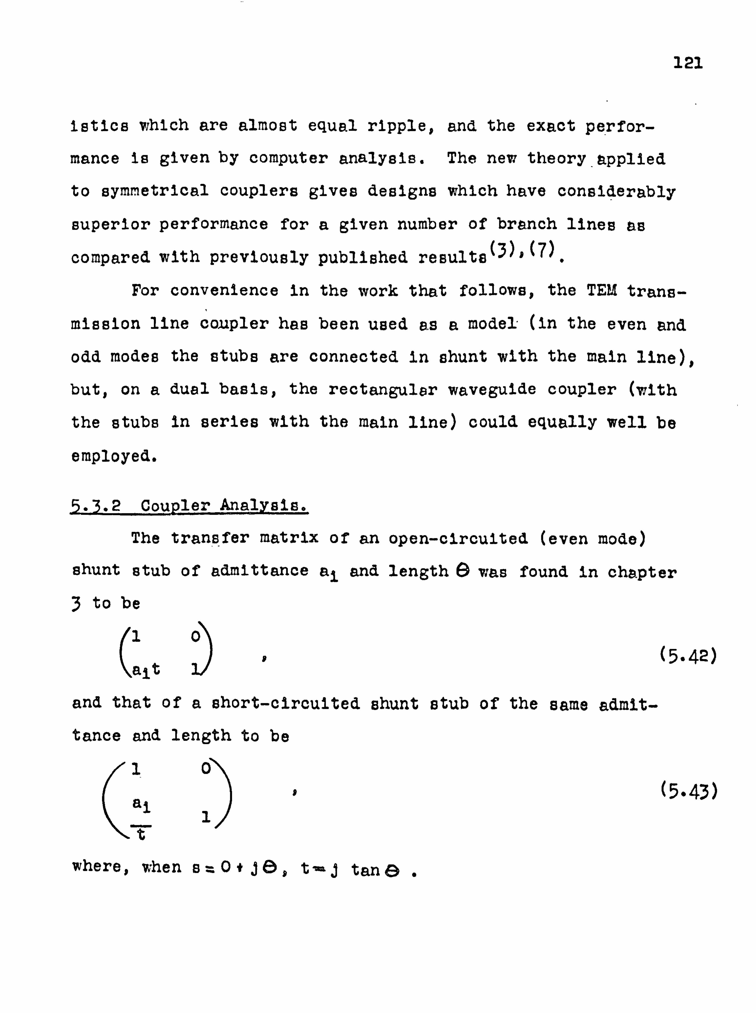
121
Tatics which are almost equal ripple, and the exact perfor-
mance is given by computer analysis. The new theory. &pplied
to symmetrical couplers gives designs which have considerably
superior performance for a given number of branch lines as (3)compared
with previously published results
For convenience in the work that follows, the TEM trans-
mission line coupler has been used as a model (in the even and
odd modes the stubs are connected in shunt with the main line),
but, on a dual basis, the rectangular waveguide coupler (with
the stubs in series with the main line) could equally well be
employed.
5.3.2 Coupler Analysis.
The transfer matrix of an open-circuited (even mode)
shunt stub of admittance ai and length I9 was found in chapter
3 to be
(5.42) Ca
it
and that of a short-circuited shunt stub of the same admit-
tance and length to be
10 (5.43)
ai 7
where, when s_ Ot J80 tmj tan &.

122
A restriction now imposed on the branch-line coupler is that
any main line (between two stubs) of electrical length 29
should be of uniform impedance, i. e., should consist of a
double-length unit element of characteristic admittance bi
having the transfer matrix 2
1 i'))
(:: i2)k 1
1-t2 t1+t2 (5.44)
The restriction imposed above has a most valuable property,
namely that Eq. (5.44) is invariant with respect to the
transformation
t-i1/t, (5.45)
except for a change of sign. Note that Eq. (5.43) may be
obtained from Eq. (5.42) by using the same transformation
(5.45)" Thus, if the transfer matrix of the even-mode
circuit is calculated, then the transfer matrix for the odd-
mode circuit is obtained using Eq. (5.45)" Mathematically,
if the even-mode transfer matrix is
Ae(t) Be(t) (5,46)
Ce(t) De(t) ,
then the odd-mode transfer matrix is
Ao B0 = (-1)n-1 7Ae(tý gel t
Co Do
Ce(t) De('l) (5.47)
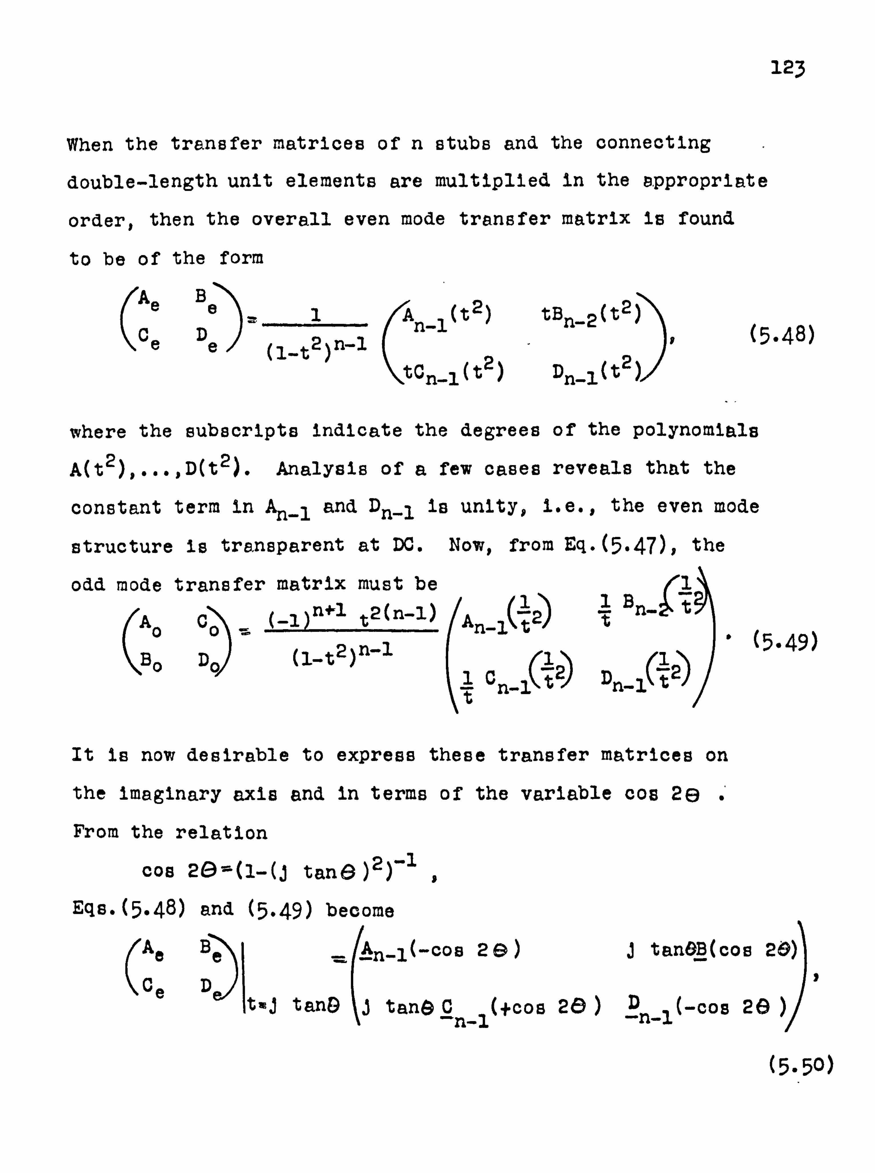
123
When the transfer matrices of n stubs and the connecting
double-length unit elements are multiplied in the appropriate
order, then the overall even mode transfer matrix is found
to be of the form
Ae Be A_ (t2) tBn-2(t2) n1 (5.48) Ce De
(i-t2)n-1 , tCn-1(t2) Dn-1(t2)
where the subscripts indicate the degrees of the polynomials
A(t2),... D(t2). Analysis of a few cases reveals that the
constant term in An_1 and Dn_1 is unity, i. e., the even mode
structure is transparent at DC. Now, from Eq. (5.47), the
odd mode transfer matrix must be
+l 2(n-1) (1 1 Bn t (A0 Co (-1)n t 2(n-1) t
Bo Do (1-t2)n-1 (5.49)
1C ýZ
D_\ t2l t n-1 n1
It is now desirable to express these transfer matrices on
the imaginary axis and in terms of the variable cos 2e
From the relation
cos 219-(I-(j tan6 )2)-I
Egs. (5.48) and (5.49) become Ae Be
4_(_cos 2 ®) , tanOB(cos 26)
Ce D' t=j tanp tans Cn_1(+cos 28 ) Dn_1(-cos 2® )
(5.50)

X24
Ao Bo An-1(cos 28) -J cote B : L(-Cos 249)
CD aj tan& -ý cot® Cn_1(-cos 26 ) (cos Dn-1 26 )
(5.51. )
Note that there are two main differences between Egs. (5.50)
and (5.51). The B and C polynomials are multiplied by j tan e
in (5.50) and by -j cot 9 in (5-51). and the coefficients
of the odd parts of the respective A, B, C, and D polynomials
differ only in sign.
5.3.3 The Approximation Problem.
As stated previously, it is desirable to prescribe the
input reflection coefficient (or the input VSWR) and isolation.
Recall that for a unit wave incident or. port Iof the
coupler, the port outputs are given by
bl, w 4( re. ro), b3 a i(Te - Toi
b4 (Te + To)
where port 2 is the isolated port and port 3 is the coupled
port. Recall also that for the even and odd mode networks I [land T are given by
(A-GDD) + (GLB-c )
r= D (A4 (LD) + (GLB+C)
(5.35)
(5.36)

125
and
2 T9 (5.37)
(A+GLD) + (GLB+ C)
where A. B. C. and D are elements of the lossless transfer matrix
and GL is the load conductance. Thus, when bI and b2 are for-
mulated, they each consist of ratios of rational numerator and
denominator polynomials. Hence it is very difficult to specify
bl and b2 in this way since the coefficients of the numerator
polynomial are closely related in a complex manner to those of
the denominator polynomial.
Consider, however, the function r /T. It will be found
that the functi'n
Fd re Te T'
has a much simpler form which may be specified by simple
Butterworth or Chebyshev polynomials. Now the important
assumption is made that re/Te and ro/To are to have as many
common zeros on the frequency axis as possible, and that in
tha6variable these zeros be symmetrical about the midband
frequency e- 45°. This statement is a crucial assumption
in the work that follows. On one hand the common zeros of fe/Te and ro/To are also the zeros of F in Eq. (5.52). On
(5.52)
the other hand, these zeros are points of infinite isolation
and perfect match, according to Ega. _(5.35). Thus, as many
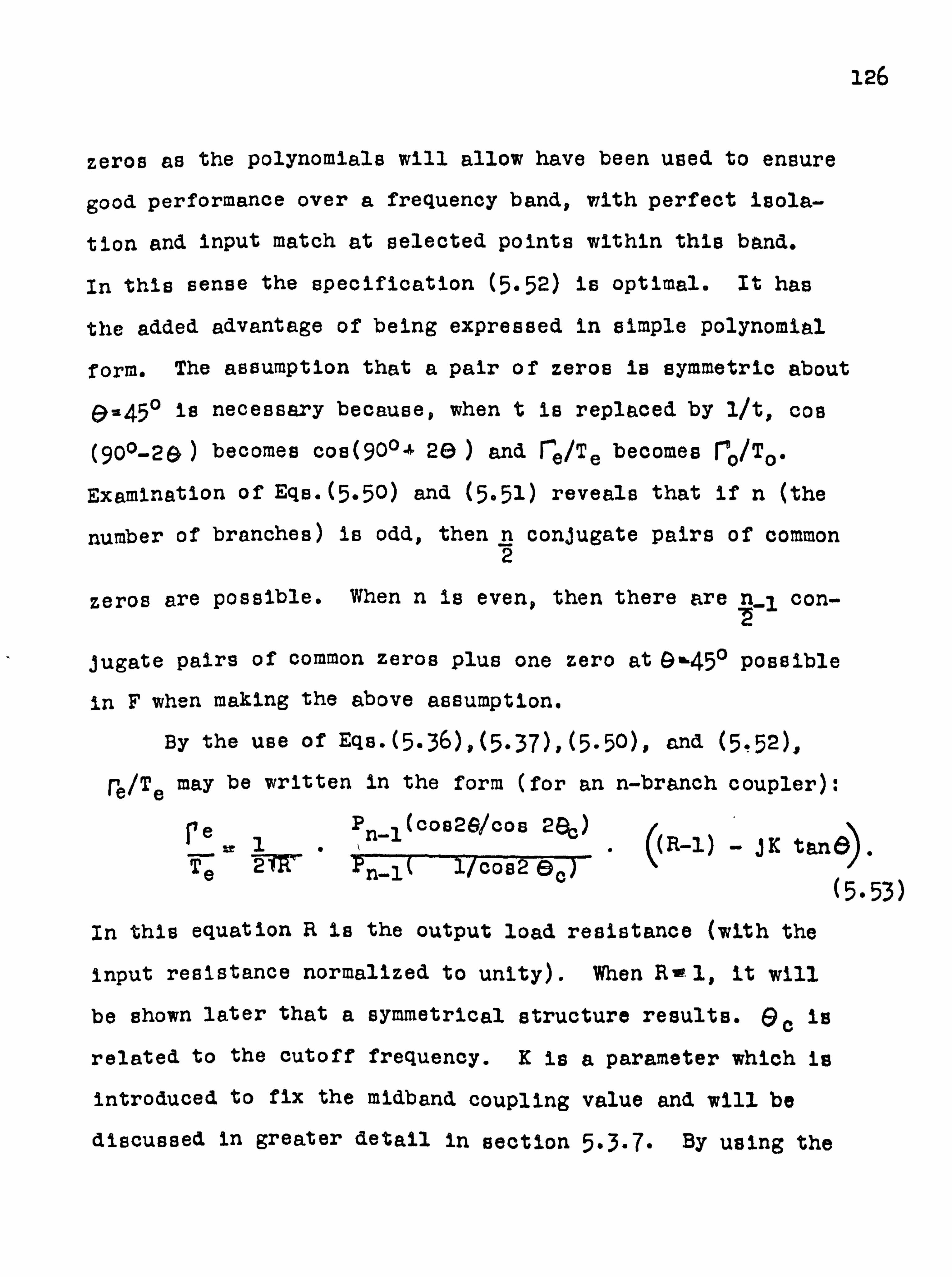
126
zeros as the polynomials will allow have been used to ensure
good performance over a frequency band, with perfect isola-
tion and input match at selected points within this band.
In this sense the specification (5.52) is optimal. It has
the added advantage of being expressed in simple polynomial
form. The assumption that a pair of zeros is symmetric about
&-450 is necessary because, when t is replaced by 1/t, cos
(900-20) becomes cos(9004 2®) and re/Te becomes r°o/To.
Examination of Egs. (5.50) and (5.51) reveals that if n (the
number of branches) Is odd, then n conjugate pairs of common 2
zeros are possible. When n is even, then there are n1 con-
jugate pairs of common zeros plus one zero at 9 -450 possible
in F when making the above assumption.
By the use of Egs. (5.36), (5.37), (5.50), and (5.52),
re/Te may be written in the form (for an n-branch coupler):
re Pn-l(cos26/cos 280)
_ ý. 1/ ((R-1) - jK tan (9). Ye 2' n-1 1/cost ®c ` -
(5.53) In this equation R is the output load resistance (with the
input resistance normalized to unity). When Rw1, it will
be shown later that a symmetrical structure results. ® is
related to the cutoff frequency. K is a parameter which is
introduced to fix the midband coupling value and will be
discussed in greater detail in section 5.3.7. By using the
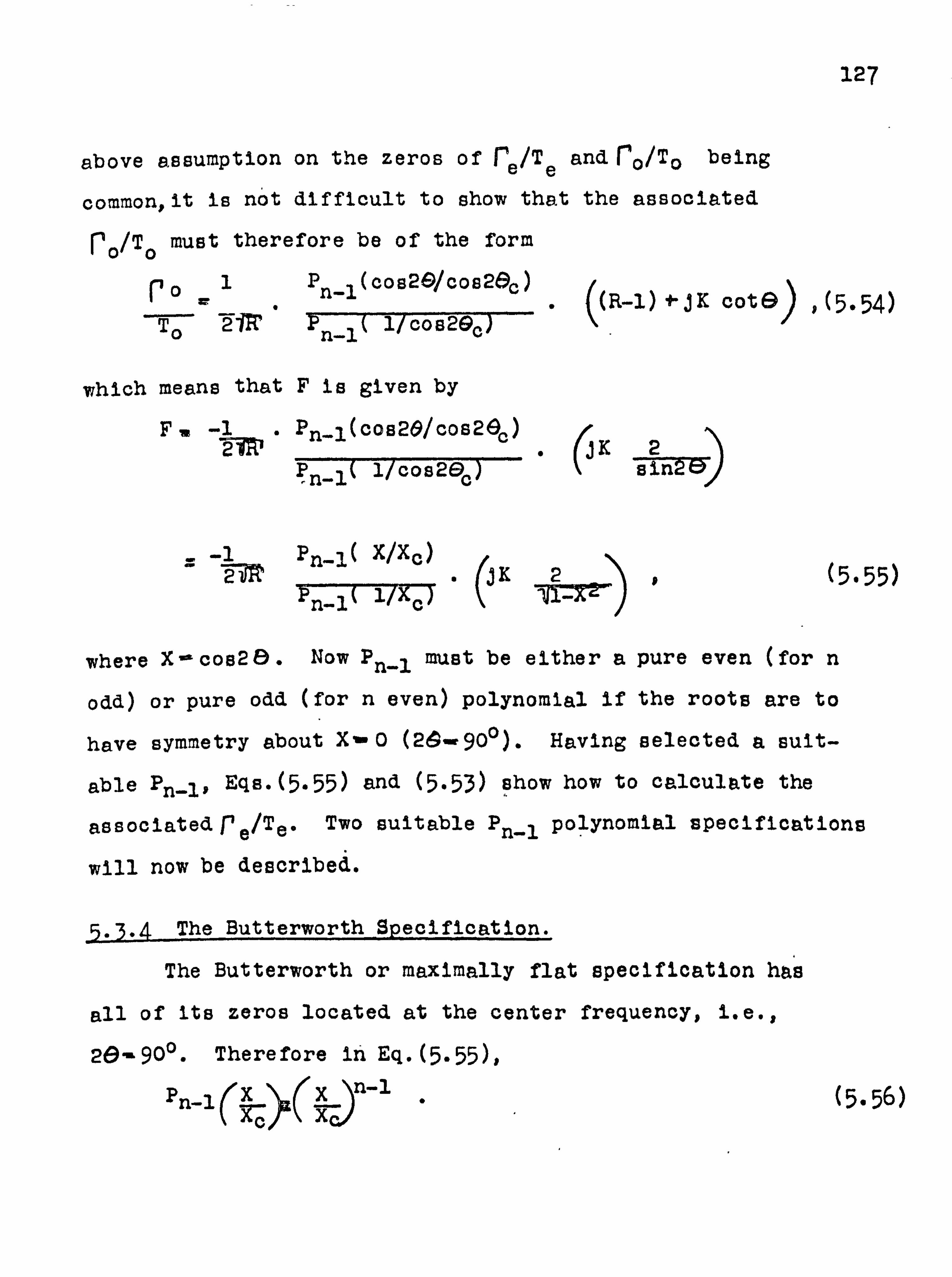
127
above assumption on the zeros of Pe/Te and ro/To being
common, it is not difficult to show that the associated
ro/To must therefore be of the form
ro1 Pn-1(coa2l /coe290) ` ((R_1)*iK cot®/ ), (5.54)
To 2T' n-1
1 cost®c
which means that F is given by
F -1 . Pn_l(cos20/cos2 Oc) (iK 2
n-1 1 cost®c since
-1 1'n-l( X/Xc) -'1" jK 2. (5.55)
n-1 77
where X- cost ®. Now Pn-1 must be either a pure even (for n
odd) or pure odd (for n even) polynomial if the roots are to
have symmetry about X+wO (26. X900). Having selected a suit-
able Pn-l, Egs. (5.55) and (5.53) show how to calculate the
associated Pe/Te. Two suitable Pn_l polynomial specifications
will now be described.
5.3.4 The Butterworth Specification.
The Butterworth or maximally flat specification has
all of its zeros located at the center frequency, i. e.,
261900. Therefore in Eq. (5.55 ),
Pn-1(? cý \ CI/
I. (5.56)
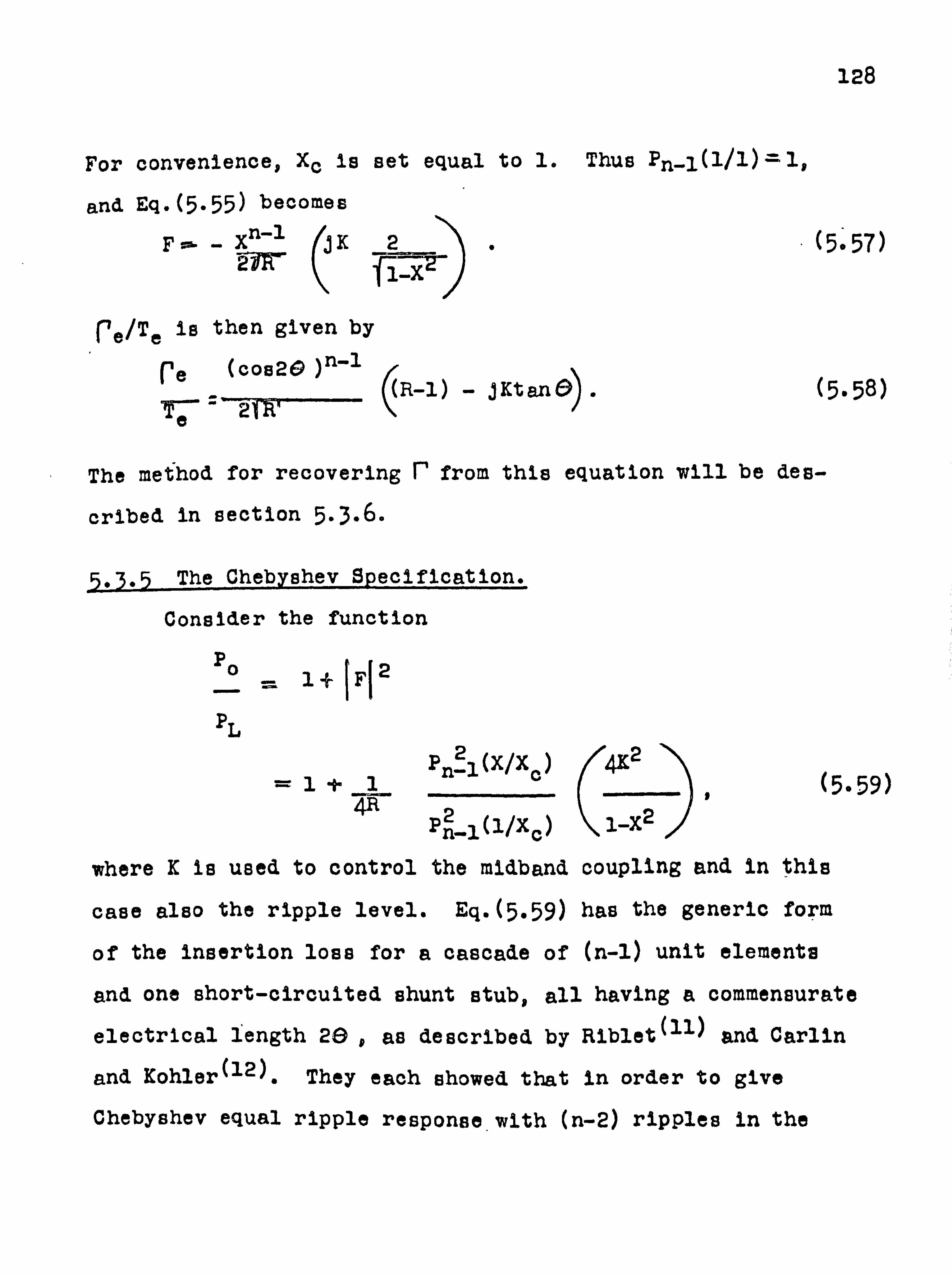
128
For convenience, Xc is set equal to 1. Thus Pn_1(1/1)= 1,
and Eq. (5.55) becomes
F_x jx 2 . (5057) 1-x
re/Te is then given by
Pe (coe20 )n-1 x-]. ) - iKtan®) . (5.58)
e2
The method for recovering r from this equation will be des-
cribed in section 5.3.6.
5.3.5 The Chebyshev Specification.
Consider the function
po = 1+ IF12
PL
1+1 Fn 2
1(X/Xc 2 ,
(5.59) 4R
pn-l(1/X c) 1-X2
where K is used to control the midband coupling and in this
case also the ripple level. Eq. (5.59) has the generic form
of the insertion loss for a cascade of (n-i) unit elements
and one short-circuited shunt stub, all having a commensurate
electrical length 29 , as described by Riblet(ll) and Carlin
and Kohler(12). They each showed that in order to give
Chebyshev equal ripple response. with (n-2) ripples in the

129
band -Xc : Xc Xe (where Xo< 1). 9 Pn-1(X/Xo) should be set equal
to
Pn-1 (YX
C-
(1 +"1Xc2 Tn-1
- (1 - 1-Xc2) Tn-3 (x) a (5.60)
cc!
where Tn(X) is again the Chebyshev polynomial of the first
kind of degree n. By inspection Eq. (5.60) is either an even
or odd polynomial in X, änd so this restriction on Pn_l(X l
CJ has been met. Eq. (5.60) may now be substituted into Eq. (5.53)
to give re/Te for this case.
The value X. in Eq. (5.60) is given by
Xc= cos(2 ®i), (5.61)
where the bandwidth of the coupler is from ®1 to ®2, with
®045° being the center frequency. If 61 = 45° - A®, then e2 - 45°+ a®, i. e. ,
®o is the arithmetic mean of el
and ®2. Obviously A ®4 45°. The bandwidth BW of the coupler
will now be defined as
BW ö A2
®o 45°
since e= 27rl . It Aä
relationship between
lower frequency wave;
go (5.62)
92
is easily seen that 1e BWw-2. The
the bandwidth BW and the ratio of
Length to upper frequency wavelength
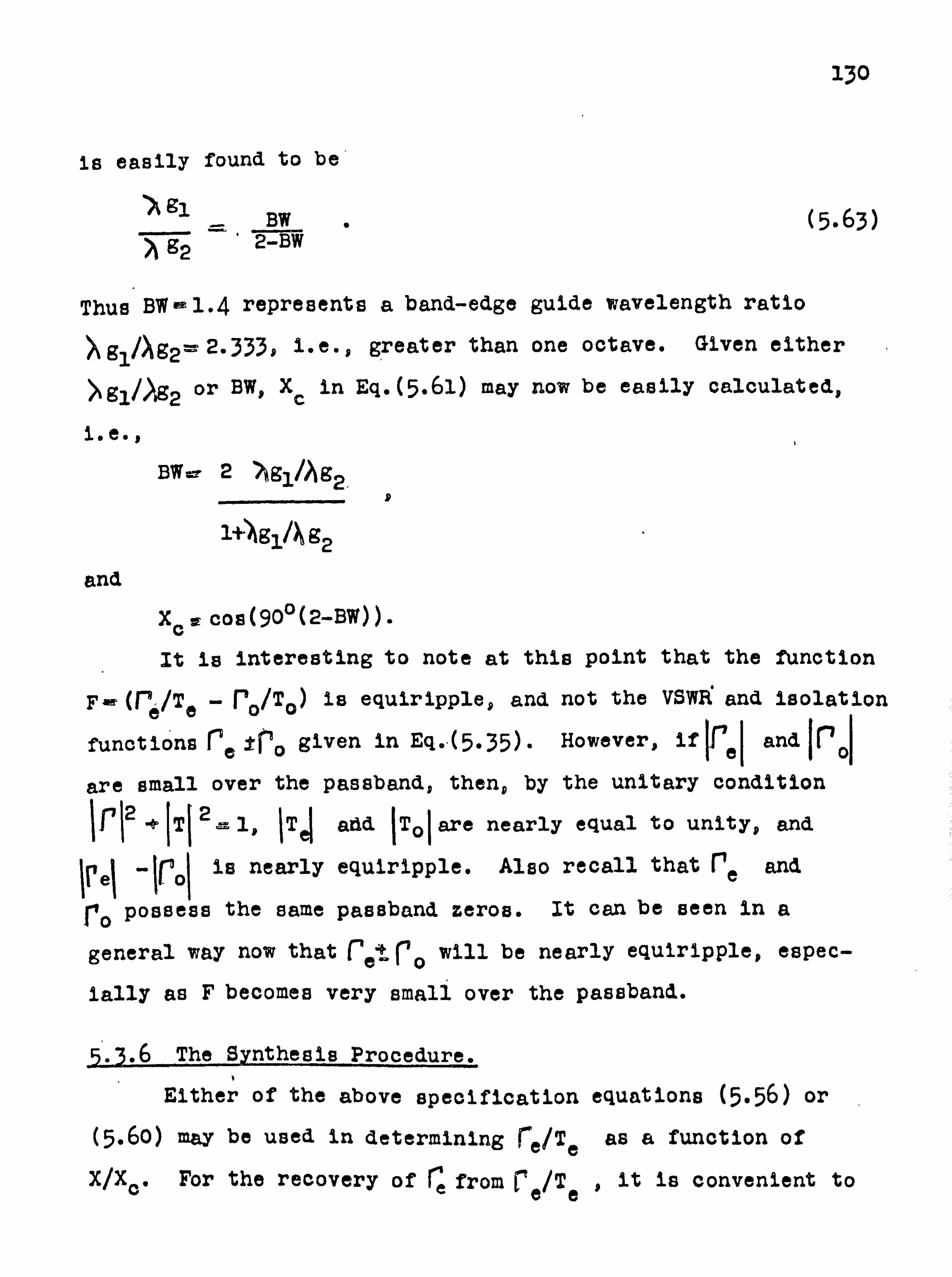
130
is easily found to be
'x gl BW (5.63) `' 2-BW il 92
Thus BW -1.4 represents a band-edge guide wavelength ratio
A g1A g2 = 2.333, i. e., greater than one octave. Given either
91/A92 or BW, Xc in Eq. (5.61) may now be easily calculated,
i. e.,
BW-- 2 ip, gl/%Ig2. D
1+) gl/) g2
and
Xc w co a (900 (2-BW) ).
It is interesting to note at this point that the function
F- (Pe/Te - r°o/To) is equiripple, and not the VSWR and isolation
functions re tro given in Eq.. (5.35) " However, if
ire I and
IrOI
are small over the pasaband, then, by the unitary condition IrI2
+ IT(2, m1, JTý
add ITolare
nearly equal to unity, and
\1'ej - Irol is nearly equiripple. Also recall that re and
ro possess the same pasaband zeros. It can be seen in a
general way now that ret ro will be nearly equiripple, eapec-
sally as F becomes very small over the passband.
5.3.6 The Synthesis Procedure.
Either of the above specification equations (5.56) or
(5.60) may be used in determining re/Te as a function of
X/Xc. For the recovery of re from re/Te , it is convenient to
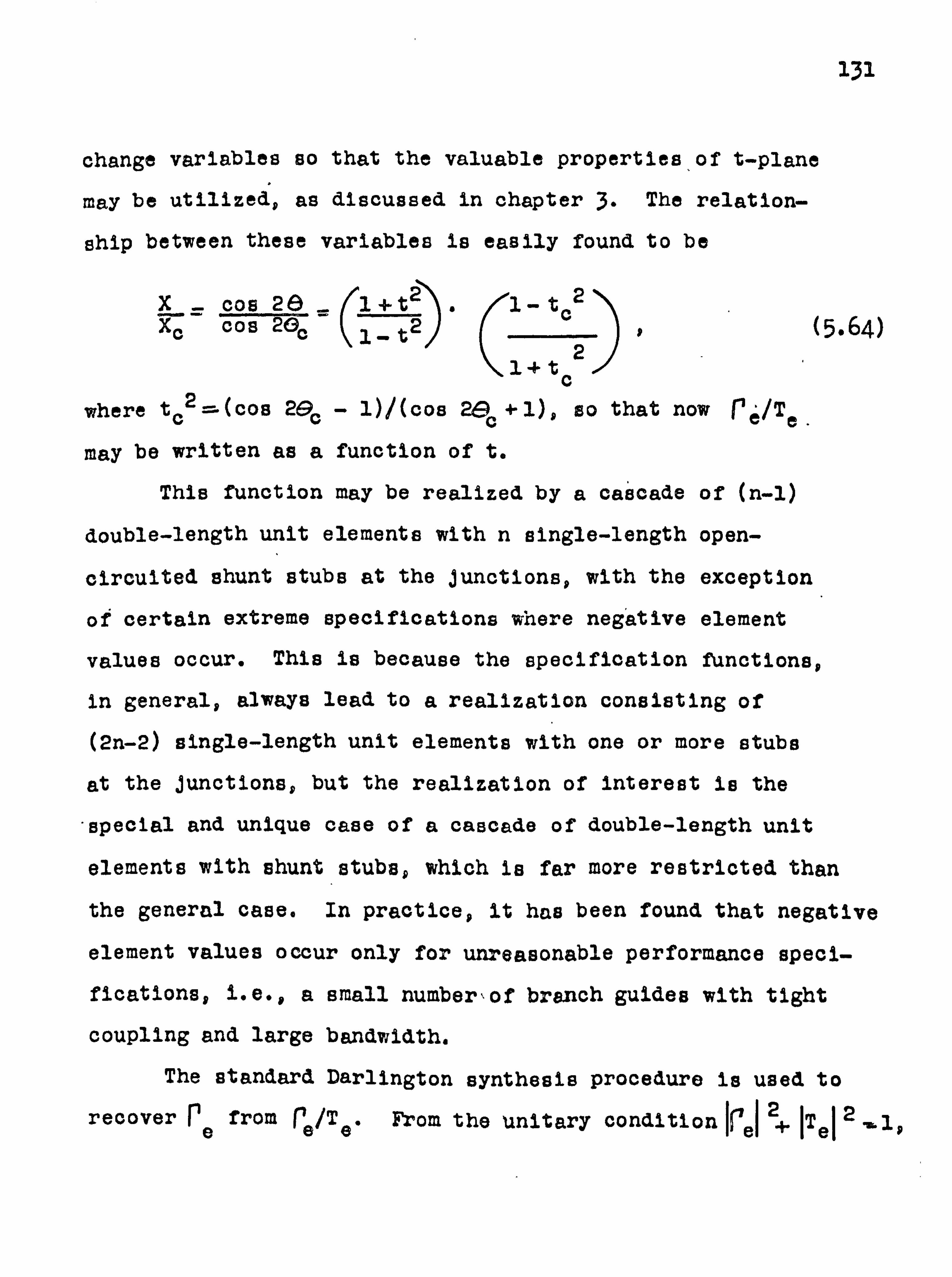
131
change variables so that the valuable properties of t-plane
may be utilized, as discussed in chapter 3. The relation-
ship between these variables is easily found to be
X_ cos 2e + t2 1- tc2 t2 Xc cos 20,
c2
(1+
t
where tc2 =(Cos 2®c - 1)/(cos 2®C +1)a so that now re/Te
may be written as a function of t.
This function may be realized by a cascade of (n-1)
double-length unit elements with n single-length open-
(5.64)
circuited shunt stubs at the junctions, with the exception
of certain extreme specifications where negative element
values occur. This is because the specification functions,
in general, always lead to a realization consisting of
(2n-2) single-length unit elements with one or more stubs
at the junctions, but the realization of interest is the
special and unique case of a cascade of double-length unit
elements with shunt stubs, which is far more restricted than
the general case. In practice, it has been found that negative
element values occur only for unreasonable performance speci-
fications, i. e., a small number'of branch guides with tight
coupling and large bandwidth.
The standard Darlington synthesis procedure is used to
recover re from re/Te. From the unitary condition Irel
+2 ITel 2
. la

X32
the modulus squared of the even-mode reflection coefficient
is given in terms ofICe/Te( as
IreI= 2 e/Tel2
a (5.65) 1+ Ire/Te 12
on the frequency axis. Definition (5.65) may, then be extended
to the entire t-plane by analytic continuation. As discussed
previously, the poles of e must be in the left-half plane.
Inspection of Eq. (5.53) reveals that for the general case
(R41) all of the zeros oflr'e/TJ 2
except for two will be
double and on the imaginary axis. These double zeros are roots of
the Pn_l function. One zero from each of these double zeros is
selected for r e. The remaining pair of roots arise from the factor,
((R-l)2 - 12t2), (5.66)
one of which will go into r e.
By trying both possibilities
and requiring that re have the form shown in Eq. (-5,36).. it can
be easily shown that if R>l the right-half plane root should
be chosen, and if R4 1 then the left-half plane root is chosen
for a zero of Pe. For the special case R= 1, the factor (5.66)
degenerates into a double root at the origin, one of which
goes tot e. Thus it is seen that for this case the numerator
of re is an odd polynomial in t. From Eq. (5.36) this means
that Aeý De in the transfer matrix, and so the network for
R =1 is a symmetrical one.
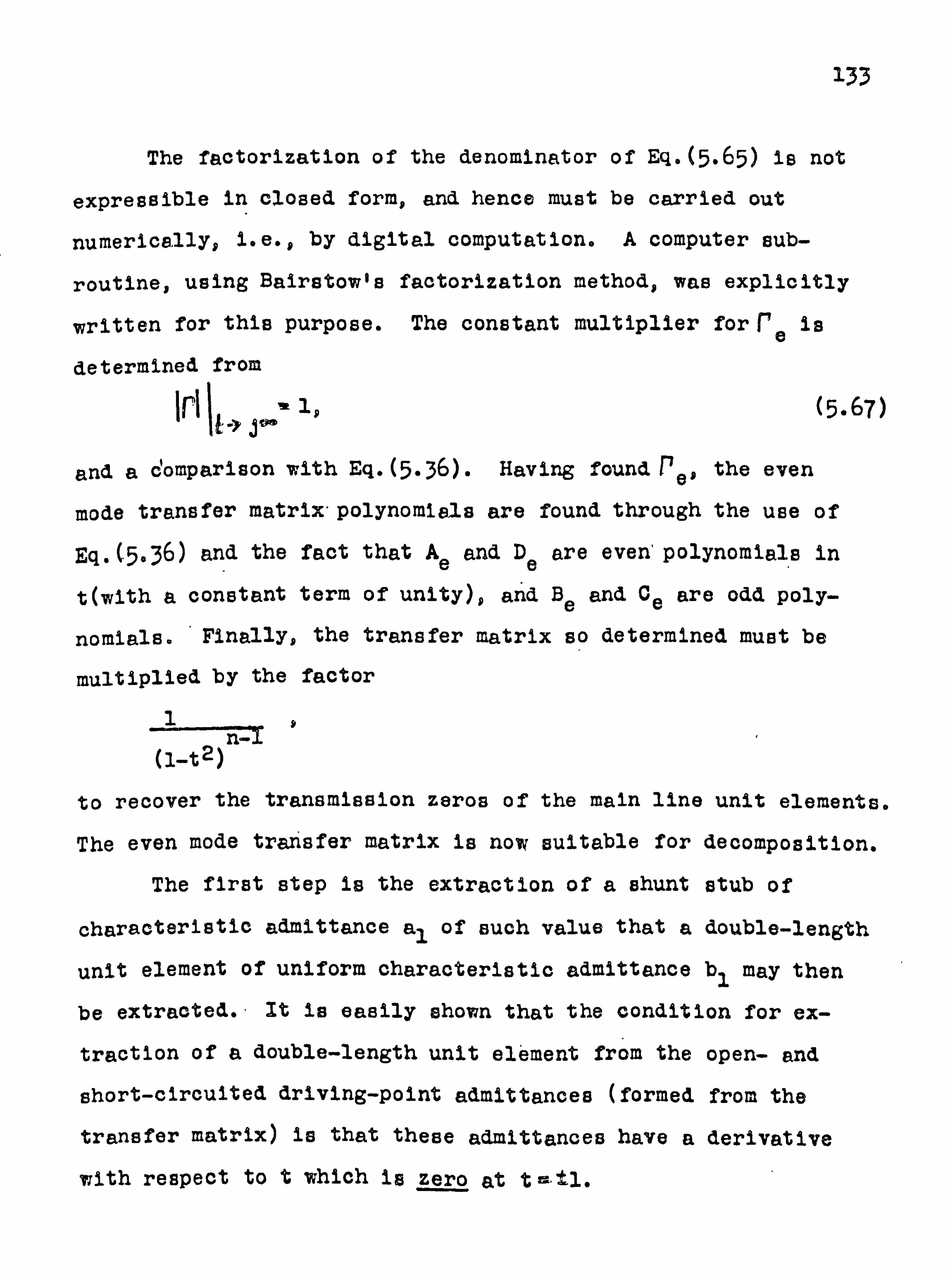
133
The factorization of the denominator of Eq. (5.65) is not
expressible in closed form, and hence must be carried out
numerically, i. e., by digital computation. A computer sub-
routine, using Bairstow's factorization method, was explicitly
written for this purpose. The constant multiplier for re is
determined from
j(5.67)
and a comparison with Eq. (5.36). Having found Pet the even
mode transfer matrix-polynomials are found through the use of
Eq. (5.36) and the fact that Ae and De are even' polynomials in
t(with a constant term of unity), and Be and Ce are odd poly-
nomials. 'Finally, the transfer matrix so determined must be
multiplied by the factor
1 n-
(1-t2)
to recover the transmission zeros of the main line unit elements.
The even mode transfer matrix is now suitable for decomposition.
The first step is the extraction of a shunt stub of
characteristic admittance al of such value that a double-length
unit element of uniform characteristic admittance bl may then
be extracted. It is easily shown that the condition for ex-
traction of a double-length unit element from the open- and
short-circuited driving-point admittances (formed from the
transfer matrix) is that these admittances have a derivative
with respect to t which is zero at t mil.
134
Using this fact, it is simple to show that when the
above condition is not satisfied, it is necessary only to
perform first the extraction of a shunt open-circuited stub
of characteristic admittance
alp Yoc (1)$ Y'sc (1), (5.68)
where the prime denotes differentiation with respect to t.
After this stub is removed, a double-length unit element of
characteristic admittance
bl= C(1 - D(1 AM 1
may be removed (by Richards' theorem), and this cycle is
then repeated until all of the elements have been removed.
-5.3.7 K Vs. Coupling.
Previously it was stated that in Eq. (5.53) E is a
parameter which is used to fix the midband coupling level.
The relationship between K and midband coupling
In a Chebyshev design, for example, to attain a
band coupling K is found to be a function of n
of branches), R, and the bandwidth. In general
found that the coupling is a monotonic function
coupling becoming stronger as K is increased in
(5.69)
is very complex.
given mid-
(the number
it has been
of K. with the
value. Some
typical values are: K Ol, coupling 20 dB; KIw . 10, coupling
12dB; K- 1.0, coupling d 4-5dB.

135
A computer program was written to carry out the entire
synthesis procedure described above. In this program both
a starting value for K and a desired midband coupling value
Cd were entered as Input data. * With this initial value for
K the program computed the associated midband coupling and
compared it to Cd. K was then modified and the process re-
peated. Five to six iterations were found sufficient to give
eight digit agreement between the calculated coupling and C.
The computer program also contained an analysis routine to
calculate the VSWR, directivity, and coupling over the band
of interest.
For one not possessing this (lengthy) computer program,
however, it is desirable to see if there is not a more direct
link between coupling and K. such that having found K the
synthesis process need only be carried through one time.
Examination of Egs. (5.35) reveals that, at midband, if
I reI' 1 and Jr. I «la then ITeIITo I 1, and the coupling is
given by b3a. ' "(Te - To). Now from Egs. (5.50) and (5,51), it
is seen that angle (Te) = -angle (To) at midband. Therefore
b3 v cos(angle (Te)),
This means that once the coupling is known, b3 is known,
(5.70)
and hence the phase angle of Te is known. Therefore a
knowledge of the phase of Te at one frequency point (mid-
band) is sufficient to specify the coupling.. It is easily
136
found 'from Eq. (5.65) that (Te[ is given by
IT el-
1. (5.71)
1+f"e
T e
In chapter 2 it was seen how the phase of an analytic
function at one frequency point could be determined by its
magnitude behaviour along the frequency axis. Therefore in
this method, starting with an initial guess for K. the cor-
responding ITel is plotted along the frequency axis in the t-
plane. It has been found that with reasonable input specifica-
tions IT4 ®1 on the
be started at t- ji.
using the methods in
culated from Esp. (5.71
line t- j0 to t- j:
Then the angle of
chapter 2, and the
0). If this is not
19 and so the plot may
Te at t- ji is computed
corresponding b3 cal-
the desired value for
b3, K is modified and the process repeated. Using the graphical
methods presented in chapter 2, each cycle in this process may
be rapidly performed. Finally, aK which yields the proper
midband coupling and has three to four place accuracy is es-
tablished, which is then used in the formal synthesis pro-
cedure. If a single coupler design is wanted, the above
method of determining K will be found to be much quicker
than successive synthesis iteration. It has the added ad-
vantage of requiring no polynomial factorizations, whereas
the factorization of a (2n-1) degree polynomial must be done
in each synthesis cycle.
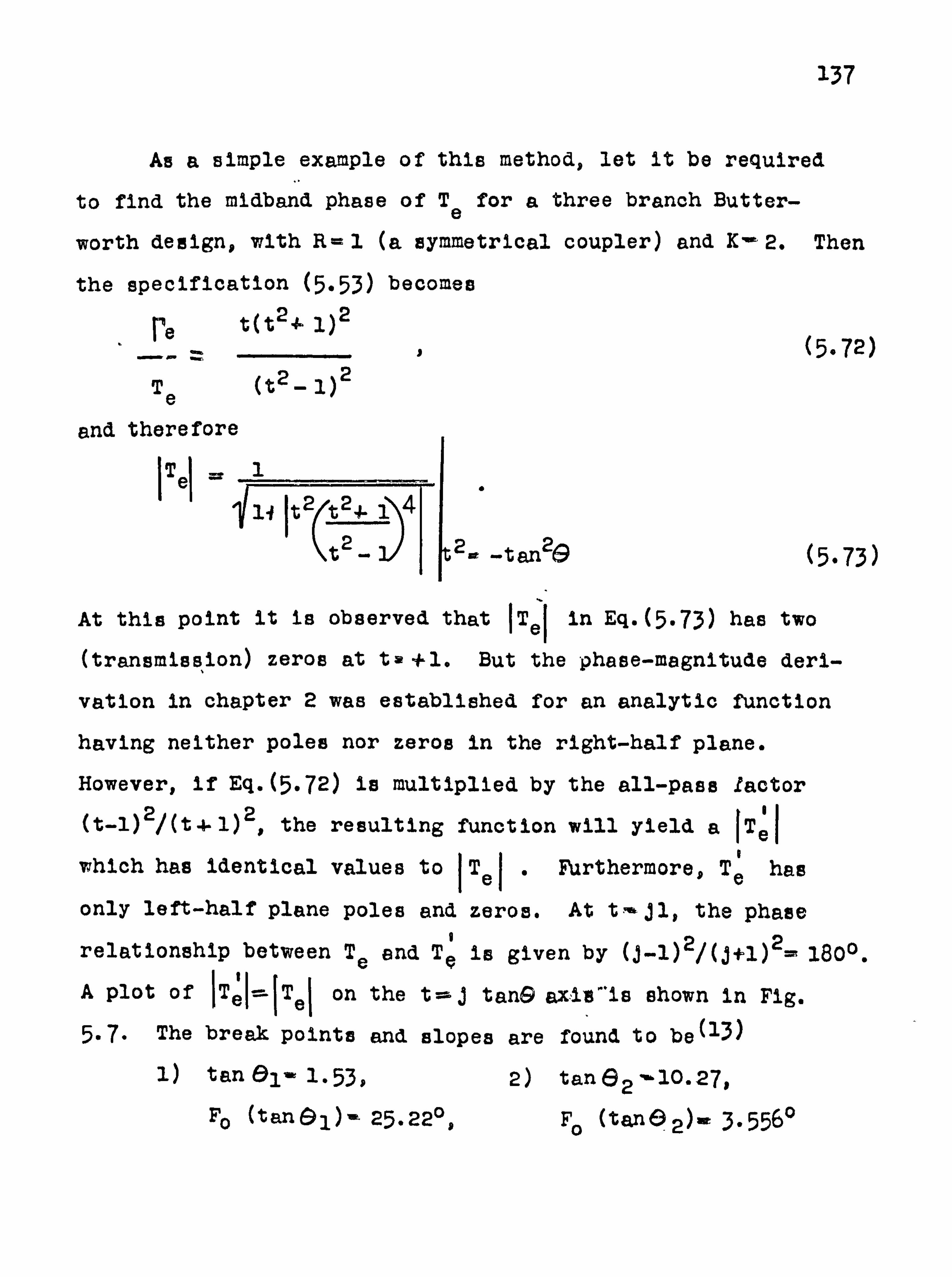
137
As a simple example of this method, let it be required
to find the midband phase of Te for a three branch Butter-
worth design, with R= l (a symmetrical coupler) and K- 2. Then
the specification (5.53) becomes
re t(t24 1)2 `.. -
(5.72) Te (t2- 1)2
and therefore
ITeI 1
1. t2 t24- 1L'\4
t2- 2_ -tan29 (5.73)
At this point it is observed that ITel in Eq. (5.73) has two
(transmission) zeros at tv +1. But the phase-magnitude deri-
vation in chapter 2 was established for an analytic function
having neither poles nor zeros in the right-half plane.
However, if Eq. (5.72) is multiplied by the all-pass ! actor (t-1)2/(t4-1)2, the resulting function will yield a
1T1e
which has identical values to I. Furthermore, Te has
only left-half plane poles and zeros. At t- J1, the phase
relationship between Te and T' is given by (j-1)2/(j+1)2= 1800.
A plot of jon
the t= -j tan® axis-is shown in Fig.
5.7. The break pointy and slopes are found to be(13)
1) tan 2) tan62+º10.27,
F° (tan®1)- 25.22°, To (tan 02)- 3 . 5560
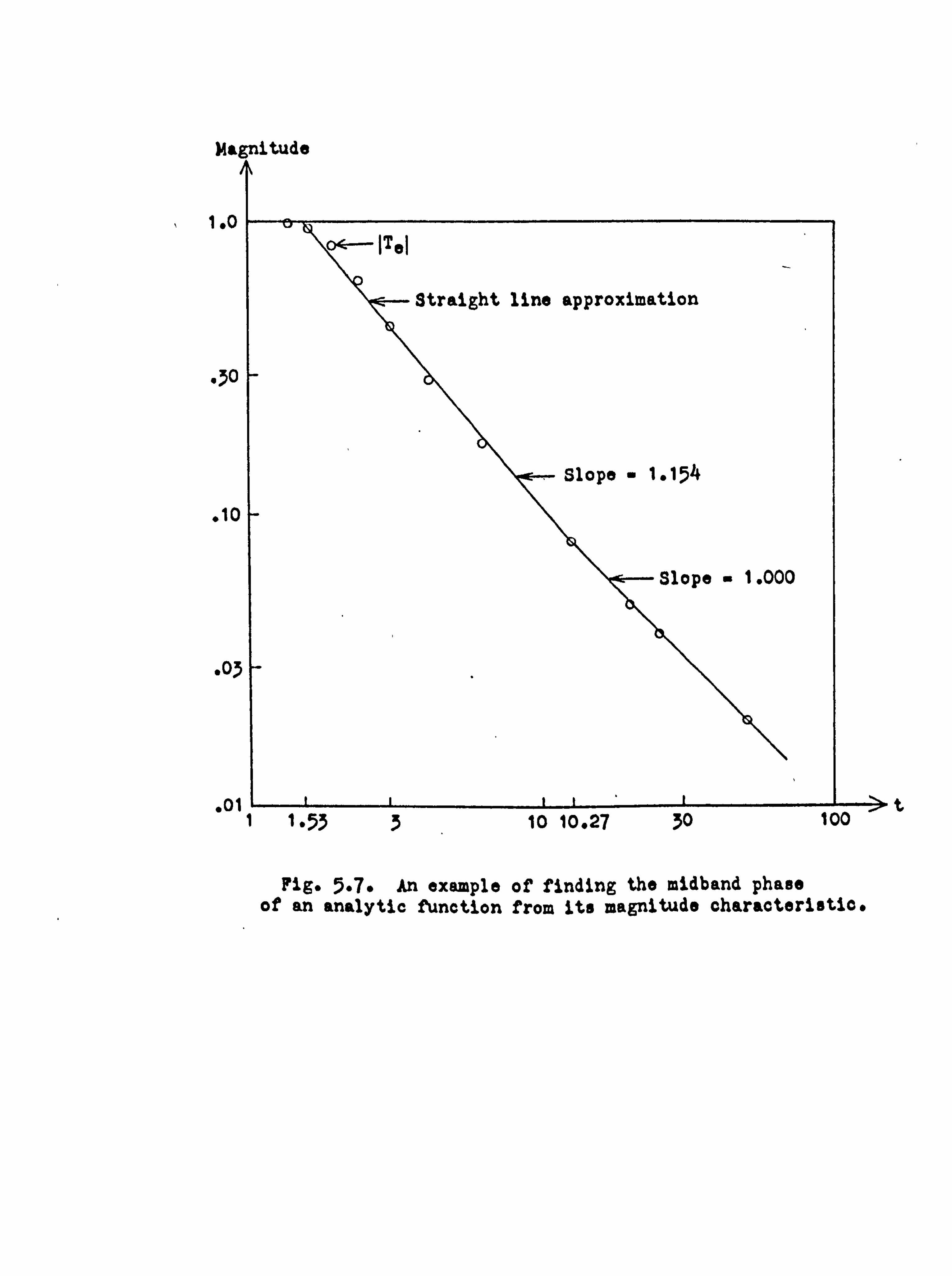
t
Fig. 5.7. An example of finding the midband phase of an analytic function from its magnitude characteristic.
1 1.53 3 10 10.27 30 100

X38
Net Slope- -1.154, Net Slope- -1.000-(-1.154)
Sl- -29.100. - . 1549
S2' *. 55°. o Therefore the net angle of TQ (j1) is 81 + 82 c-28-55. The
final angle of Te(jl) is then given by
1800 - 28.55°. The example specifications were next entered into the
computer synthesis program. At midband the angle of Te was
eventually computed as
180° - 28.520,
which shows close agreement with the graphical method, and
thus justifies the validity of the above method.
j. 3.8 Example of the Synthesis Procedure.
Consider the design of a three branch asymmatric Butter-
worth coupler with the input specifications R -2 and K- 1.
From Eq. (5.58),
re 1-+-t2 (R-1) - Kt . (5.74) Cý Te 21 1- t2
Then
Pe (t24 (R_12 - K2 (5.75)
Te 1- t2 4R 4R

139
From Eq. (5.65) 1re2 is given by
2 2 re
I del T e (l+t 24 (R_12 - K2 t2
1+ re 2 4R(1-t2 4+ (1+t2)4C(R-1)2 - K2t2
Te
(1+t2)4 (i-t2) (5.76)
8(1-t2)44 (l+ýt2)4 (1-t2)
Recall that when R> 1 the right-half t-plane factor of
((R-1) 2- K2t2) is chosen as a zero of r-. The numerator of
re thus has the factors
(1+t2)2 (i-t)-, - i-t ß-2t2- 2t3+ t4- t5. (5.77) The denominator of (5.76) is factored using the Bairstow
method. It is found that when this factorization is per-
formed and the left-half t-plane roots are multiplied back
together, re is given by
ýe K2 1-t + 2t2 - 2t3 + t4 - t5 (5.78)
3.0004-12.220t* 20.056t2
-+ 15.904t3+ 3.068t4 +-t5 K2 may be found by comparing Eqs (5.76) and (5.78) as t-ý j °° . It is seen that K2 = 1. (See Eq. (5.67)).

140
Now according to Eq.. (5.36) re must be of the form
re (Ae-GtDe)}(GI, Be-Ce)
" (5.36)
(Ae + GLDe) + (GLBe +- Ce)
It has previously been shown that the constant term in Ae and
De is unity. In Eq. (5.36 ), 0L-v 1/R= -5. Thus the constant
term in the numerator of Eq. (5.78) should be . 5, and that in
the denominator should be 1.5, i. e., th4 numerator and denomi-
nator of Eq. (5.78) are scaled by . 5, resulting in
Peu- (. 500+2.000t2+- (. 500)t4) 4-(-, oot-1. ooot3- . 500t5) (1.500+10. o28t2-4- 3.034t4)', -(6. slot+ 7.. 952t3+ . 500t5)
(5.79) Comparison of Egs.. (5.36) and (5.79) reveals that the elements
of the transfer matrix are given by
Ae 1.000 + 5.514t2 4 1.767t4, Be = 5.610t + 6.952t3,
Ce = 3-305t+4-4760+ .. 500t5, Dew- 1.000+9.029t2+ 2.533t4, (5.8o)
and the even mode transfer matrix is therefore
1------ Ae Be
(1_t2)2 cD (5.81)
ee
Notice that the t5 term in Be is missing, as expected by
Eq.. (5.48).
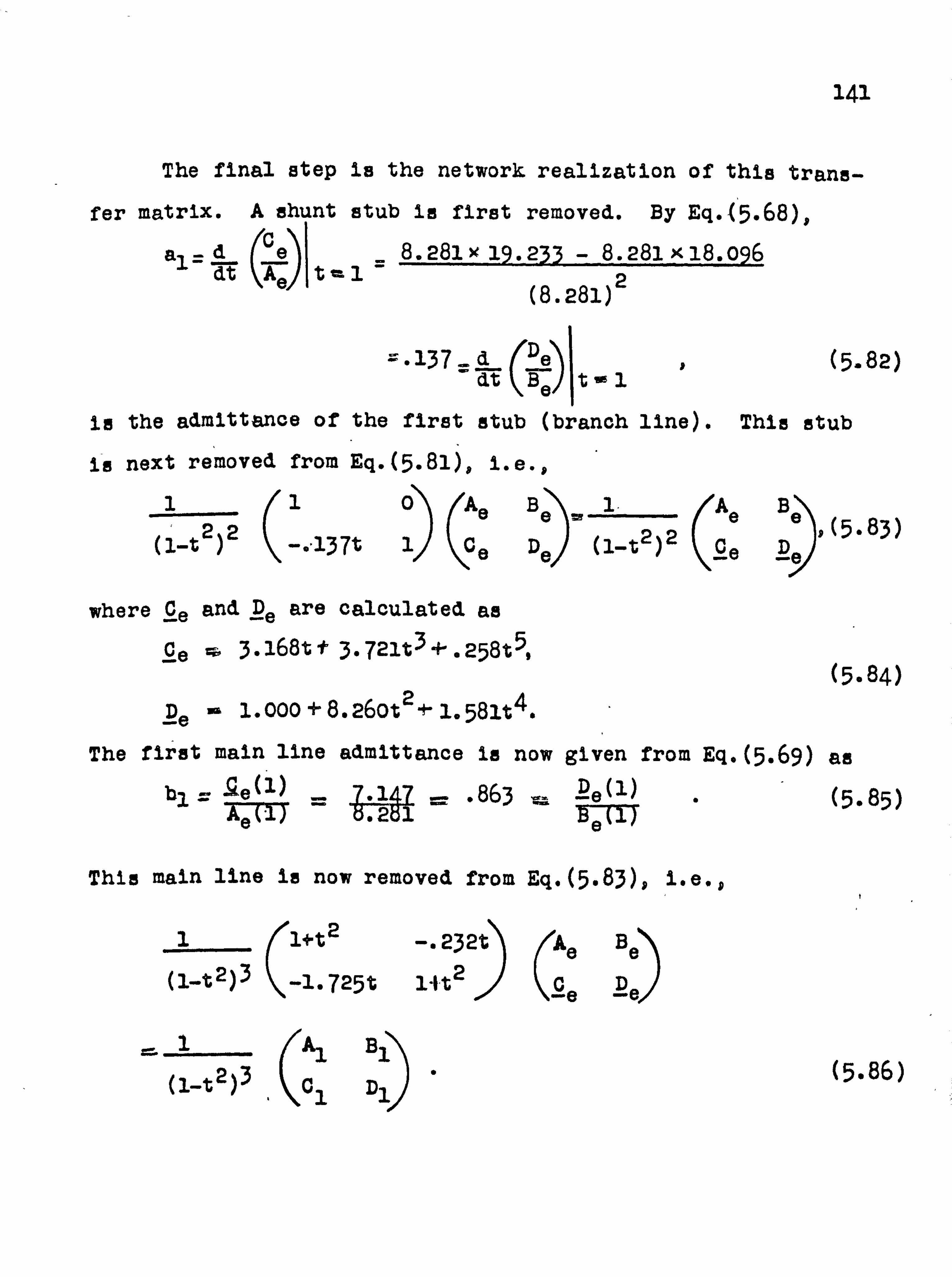
141
The final step is the network realization of this trans-
fer matrix. A shunt stub is first removed. By Eq. (5.68),
a1 =d (Ce'\
8.28l x 19.233 - 8.281 x18.096 dt A tml -2 (8.281)
="137_d De (5.82) dt Be tý1
is the admittance of the first stub (branch line). This stub
is next removed from Eq. (5.81), i. e.,
10 (Ae Be-1 (Ae Be 22 , (5.83)
(1-t ) -. -137t 1 ce De (1-t2)2 ce De
where Ce and De are calculated as
Ce 3.168t 1° 3.721t3 +. 258t5, (5.84)
De 1.000+8.260t 2 4- 1.581t4.
The first main line admittance is now given from Eq. (5.69) as
hl _ ße(1) = 7.147 = . 863 Re (1) (5.85)
iT 6.261
This main line is now removed from Eq. (5.83), i. e.,
1 1+t2
(1-t2)3 -1.725t
(1-t2)3 cl D1
f
-. 232t Ae Be
1"It2
(-C
e De
0 (5.86)

142
For the resulting transfer matrix to be of lower degree, it
is necessary for A1, B1, Cl, and D1 to contain a factor
(1-t2)2, which they will have, of course. After performing
the algebra, it is found that the resulting transfer matrix is
1 C1. -1-1.17ot2 3.292t (5.87) " 1-t2 442t 1- . 257t3 1ß'1.579t2
The above removal cycle is now repeated until all of the
elements have been removed. The admittances for the coupler
of the above design are found to be
1.000 3 b07 o0
. 137 . 176 . 052 r (5.88)
1.000 . 863 . 607 . 500 The frequency performance of this design may now be
determined by analysis. It is found that the midband coupling
value is 9.49 dB in this example. Also at midband the VSWR
should be 1.0 and the directivity infinite, as is verified by
a midband analysis. At a bandwidth BW' 1.1, the performance is
Coupling - 9.35 dB,
VSWR = 1.013, Directivity -30.15 dB,
which shows the degradation in performance from midband for
this example.

3 43
5.4 Discussion of Computed Results. (9)
-. 4.1 The Symmetrical Case
Results have been computed for a large number of cases
of practical interest, and the element values are presented
in Tables 5.1 and 5.2. Since the couplers are symmetrical,
the immittance values tabulated are given as far as the center
of the coupler. In Table 5.1 the bandwidth BW-), gc/ > 92 cor-
responding to points where the directivity falle to 20 dB is
given for each case and also the band-edge coupling (B. E. COUP
(dB)) and the VSWR at these points. The performance is symmet-
rical with respect to electrical length 19 on each aide of midband
(where Go- 45°). In Table 5.2 the worst VSWR and lowest direc-
tivity over the band are given as well as the band-edge coupling
for each case. It is worthwhile noting at this point that for
a stripline realization the immittances presented in the Tables
correspond to characteristic admittances (normalized to 1 mho).
The dual is true for the waveguide case.
The designs in Tables 5.1 and 5.2 have been mainly re-
etricted to cases where the directivity of the couplers is
greater than 20 dB. It has been established that the results
obtained from the synthesis procedure result in a considerable
improvement over existing designs. It is seen also that the
new information includes specifications which have previously
not been presented, and it is shown possible to design branch-
guide couplers with good VSWR and high directivity over large
bandwidths, i. e., of the order of one octave or more.

GLFMENT VALUES FOR UUTTLRWORTH BRANCH-GUIDE COUPLERS FOR /I-3 TO 9 BRANCHLS
t1aAMOM oVI116 tMYt1TM t7 MAIN LINZ ! ! 1.7ANC1S
eour ýwr 71s We " "f "7 IN 1' 1 ° 1° ° % re) 1 s , t" 3
I. uu79 tS 14.6 1.18 1.01 . ua96 0.1821 . 1.0128 to 9, S" 1.17 1.03 , 1623 0.3850 I. dW5
8 7.6c 1.16 1. W 0.2076 0.11607 0 1.0757 6 5.68 1.15 1.07 . 2697 .
: 6"n 1,1312
0.70 1.11 1.09 0,3078 0.7878 1.1877 " 7.70 1.11 1. t 0.7553 0.9974 1.2577 ! 2.69 1.14 1.1 0.8149 1.3432 1.7774
2.5 2.24 1.13 1. t o 4513 1.6188 " 4 69 3
i"78 1.17 1. 0.89°1 I t. 0329 59 96
: 1
to 19.0 1.29 1.01 u. u253 O. IY/52 1. uuq 1.003
15 1l. 1 1.28 1.02 0.0156 0.1! 35 9.0(179 1.0176 10 9.09 1.96 1.08 0.08¢1 0.! 578 1.0281 1.0632
I N
7.1! 1.25 1.05 0.1088 0.3357 1.0486 1.1101 6 5,2" 1.23 1.08 0.1328 0.8646 1.0875 1.2022
5 14.22 1.23 1.1 0.1698 0.5635 1.17W 1.2850 3.71 1.82 1.1 0.1688 0.7083 1.1702 1.4165
. 3 2.32 1.01 1.10 0.1895 0.9466 1.2510 1.6888
!. S 1.09 1.21 1.23 0.0000 1.1777 1.3125 1,8*22
t 0. 2102 1.427° 1.799! f, 1Ni
1a. s 1,36 1. . 0119 O. U" u"uM 1.0017 1.00+16 15 13.5 1.36 1.92 . 0233 0.091! 0,1318 1.0018 1.0156 lV . 67 1,32 1" "0126 0.1665 0.2542 1.0167 1.4)5/3
" . T0 1.31 1-07 . US12 0.2172 0.3411 1.1*86 1.1013 6 8.76 1.310 1.1 . 0681 0.8929 0.4857 1.0523 1.1896 f 3.92 1.29 1.1 0. urlu 0.3860 0.6ur8 1.0727 1.2696 f . 91 1.18 1,1 . 0857 0.4204) 0.7931 1.1146 1.3991 3 . 01 1.17 1.22 "0941 0.5318 1.1383 1.1541 1.6316
6. s 1.67 1.16 1.2 . 0976 0.6148 1,4457 1.1926 1,8701 t t. 16 1.116 1.7 0.0999 0.7323 1.9616 1.0470 1.1417
W 17,9 1.41 1.06 0.4)066 0.4)317 0.06113 1.0008 1.0033 9.4)09" is ,:. 9 l. w l. 0 u. 012u 0.0571 0.1119 I. Wti 1.0195 1.0165 10 a. 12 9.37 1. 0.0224 0.1u48 0.74)96 1.0091 1.0431 1.0696 " . 19 1.36 1.00 . 0286 0.1352 0,! 798 1.0162 1.0769 1.1146
8.39 1.34 1.11 . u364 0.1774 0.3957 1.0302 1.1455 1.1399 5 3"36 1.34 1.1 0. Ow8 0.2053 0.494)5 1.0113 1. N+75 1.3880 4 2.50 1.33 1,1 0.0453 0. tw6 0.6103 1.0610 1.3079 1.5311 3 1.73 1.31 1. . 0492 0.18714 0.916! 1.0917 1.4876 1.8832
1"5 1.71 1.31 1" . 0506 0,3179 1.1681 1.1154 1.6386 8. /u! y 0 . 99 1 . 30 1. . u51u 0,3360 1.58if 1.193 1,8739 1,7433
e. s. e11A147H OVIDa 44MA1Cas -All 11. IN2 7". -gM; WA LS Ät Vflal ý1 ýa S% ay e Y 4 F-
l a S n
a0 73 1.46 1.02 0033 0.0193 O: 9 0. 1. t. 0u2 1.0050 IS 12.5 1. YY 1,03 "0062 0.0350 o. b6142 0.1111 1.0013 1.0076 1.0171 10 7.70 1,141 1.06 . 0118 0.0646 0.1564 0.2091 1.0049 1. IV93 1.0663 8 5,77 1.140 1.08 , 0132 0.0730 0.2063 0.4817 1.0090 1,0545' 1.1186 6 4"IX' 1,38 1.12 0.0196 0.1072 0,2946 0.4075 1.0170 1.100'1 1.8316 ! 3.11 1.37 1.15 ., 0220 0.1222 0.3454 0.5166 1. O*1 1,1044 1.3392 4 2.26 1.36 1.19 o, o244 0.1345 0.4367 0,74)01 11.0362 t. PN6 1.3239 3 t. 8 1.35 1.25 0.0265 0.1593 (1.5142 1.070) 1.0537 1.3341 1.3861
1.5 110 1.34 1.30 0,0271 0,1700 0.7276 1.4365 5.0682 1.44116 2,2214 a
. nae 1.33 11:
391 0,0472 0,1810 0.91127 4.11_99 I$. (Mo3 1.6u7r 2, POW
n A 20 16.9 1.49 1.02 0. W17 0.0115 0.0332 0.054: 1.000' 1.0014 1, IX139 1Op5S 11 12.1 1,17 1.04 0.0032 0.0210 0,0599 0.071 1 (. 0)07
1 1.001'1 1.0137 1 019
10 7.33 1.44 1.06 . X162 0.0392 0.1104 0.1819 I t. 00?. 7 1.0t! w1(. 0931 1.0746 0 1.43 1.43 1.09 0.0061 0.0505 0.1440 0.2443 I. 0U149 1.0342 1.0973 1.1373 6 3,66 1.41 1.13 1.0106 0.0648 0.1935 0.3517 (. 0099 1.0662 1.1919 1.27143 5 2.93 1.140 1.16 0,0119 0.1)737 0.2291 0.4447 1.0136 1.1951 1.2817 1.110901 Y 4.00 1.39 1.20 0,0133 11.0893 0.9785 u. 6o15 1.1'401 1.14 t" 1.14331 1.6881
1.25 138 1.29 0,01145 0.0913 0,3548 00210 I. 11 1,2x4.1,7354 9.1476 0.5 . 690 1,37 133 0,01149 0.0952 0.14199 1: 24 01 1.0100 1.004 2,01052,6397
I . 691 1.35 1.34 1
0,0189 0,0979 0.144/) 1,8466 I. 4I930 10 4.4811 3_51o*
0 1 .5 1,52 (. Oa . 0009 O. OU61 0.14114 0.0436 0.0534 1.018)1 1. OYU9 1.110911 (. 0099 11 11.7 1.60 1"M "0017 0,0124 0.0601 0.0781 0.0964 I, db3 1.102.1 1.0100 1.0182 10
, 95 1,. 147 1.118 , W33 0,0235 0.0751 0.1435 0.08(2 1.801 1.0110 1,0396 1.0716 d 5.21 1.45 1.09 . 00Y3 0.03014 0.0976 0.1934 0.6451 1.0427 1.11,114 10731 . 1,1330 6 3.33 1.44 1.11 . 0057 0.0392 0.1265 0.1725 0.3601 I. Q19: 1.0411 , 1NA 1 1.3691 !
. 39 1.43 1.17 . 0063 0.0441 0.11490 0.3381 0.4650 5,0o76 1.061)6 , Its 1.4007
1.75 1.94 1.34 , 05'113 0.10092 0.1750 0,4401 0.6517 1.0113 . 1.0909 1.3985 1,6493) 3 1.09 1.40 1.98 . 0080 0.0937 0.909E 0.6185 1.0663 1.0179 1.1446 1.5503 2.1686
9.5 , 100 1 . 39 1.32 1 . 0082 0.0!! 3 0.2318 0,8428 1.9180 1.0232 1.1891 1.75415 0.6919
0 1
, n0 1: 381 , 59 ,: 1,35 . 0037 0.0397 0.9690 1.1 4 4. $ .0 13 1f 79 P. op" . 693
TABLE 5.1.
ELEMENT VALUES FOR CHEBYSHEV BRANCH-GUIDE COUPLERS FOR n-3 TOS BRANCHES
21WICH OVID* I"ýMI1^4NCES MAITI LYRE 1.4, cEs 71[2 00or . OVr DIR. V3WR °1 3 '! S b4
tfý
tu i). 9 36.6 1. uu0 0509 0.0993 t. 0089 t3 4.9 35.9 1. o0) . 0911 0.1795 1.0130 10 9.56 34.4 I. OW . 1656 0.3385 1.0451
1.1 8 7,15 33.5 1.007 . 2124 0.4512 . wm 6 5,12 32.5 1.015 . 2761 0.6301 1.1369 3 4. P3 31.9 1.021 . 3174 0.7686 1.1874 4 303 31.2 1.030 . 3681 0.9729 1.2641 3 2,73 30.4 1.043 . 4330 1.3103 1.3899
t0 19.5 24.3 1. . 0731 U. 0948 ,1 15 14.3 23.5 1.009 . 0957 0.1703 . 0134 10 9.42 21.9 1.024 . 1761 0.3177 . 0471
1. t 8 7.36 11.0 1.040 . 2210 0.4107 1.0208 6 5.34 19.9 1.073 . 3008 0.5830 . 1434 S 4,32 19.3 1.102 . 3499 0,7087 . 2011 4 3.30 18.3 1.150 . 4130 0.99556 . 2860 3 2.29 17.7 1.236 . 5007 1.2176 . 4391
8u 1 .9 113 . 0573 0, 3
1.3 1S 13.5 13.9 1.0¢9 . 1013 0.1332 . 0148 I I Li
IC ^". 65 14,9 1,073 . 1962 0.2796 1 Ll
TABLE 5.2.
OVID{ I"1121SANCES 11 MAMI LTIM I-{ "AAKH OVIOt I'MITrAHOSS 4AIN LflR 104MAMU 1
b1Rf7T{NCCS ýý sý "{ 42 º{ ºý º{ i1f{ OOUý OUr Wai vmm "I '{ '3 {{ 1 ºt
S
_L 1 ... ýI n_4
w 19.9 58.6 1. 0.0938 0.07N 9"0018 1.0031 1S 14.9 57.8 1.000 0.065 00344 9.0090 1.0177 10 9.97 35.5 1.000 0.0683 0.2513 1.00197 9.634
1.1 6 . 96 54.4 1.001 0.9073 0.3328 1.049", 1.1106 6 5.156 53.1 1.001 0.1371 0.4607 1.0999 1.2a81 S 11. '6 51.3 1,001 0.1570 0.5599 1.1040 1.6877
º . 66 51.4 1.003 0.1753 0,7037 1.1758 1.8207 3 . 06 50.3 1.004 0.1979 0,941" 1.0606 1.6+7D
19.5 0. . OW 0.0215 04730 1,0015 1,0033 IS 14.6 39.1 1.001 0.0497 0,1318 1.0003 1,0177
10 4.47 37.1 1.0014 0.0919 O, 446 1.0307 1,1640 1.2 6
.9 75.9 1.007 0.1171 0.3213 1.0935 1,1111 6 5.43 39.6 1.013 . 1513 0.1474 1.0977 1.29 S 41.42 33.7 1.019 . 1706 0.9432 1.1357 1611915 º 3.41 31.8 1.027 . 1973 0.4151 1.1944 1.4341 3 2. *' 31.6 l 143 0.19699 0.0059 1.2496 9.6839
w IR. 8 19.6 1.007 0.0306 0.0699 1.0027 1.0033 H 13.9 18.0 1.07 0.0}39 00210 1.0003 1,0179 10 0.76 29.0 1.010 , 1017 0.1310 1,0304 1,0659
1,3 8 6.79 94.7 1.073 . 1365 0.3013 1.0606 1,1199 6 4,67 13.2 1,059 0.1900 0.4193 9,1111 1.2150 5 3.66 26.3 1004 0,11097 0.5006 1,15115 1.3076 º 1.66 11,0 9.128 0.2450 0.68! 0 1.0713 I, 13ý 3 1.71 90.0 1,197 . 71916 0.1'405 1,7577 1.7äI9
go me It. U339 " 1.00 1 1" 15 12.9 19.6 1,01' . 0666 0.1183 1.0107 1,0181
1.8 to 7.71 17.4 1.067 . 1991 0.6067 1.0109 1.0669 6 3.67 16,1 1.110 1726 0.1683 1,072 1.1190 6 3.61 14.9 1.501 . 1377 0.3663 1,137 1.261 S 1.66 13.5 1. PUS 0.1375 P-1960
. 1.3247 .
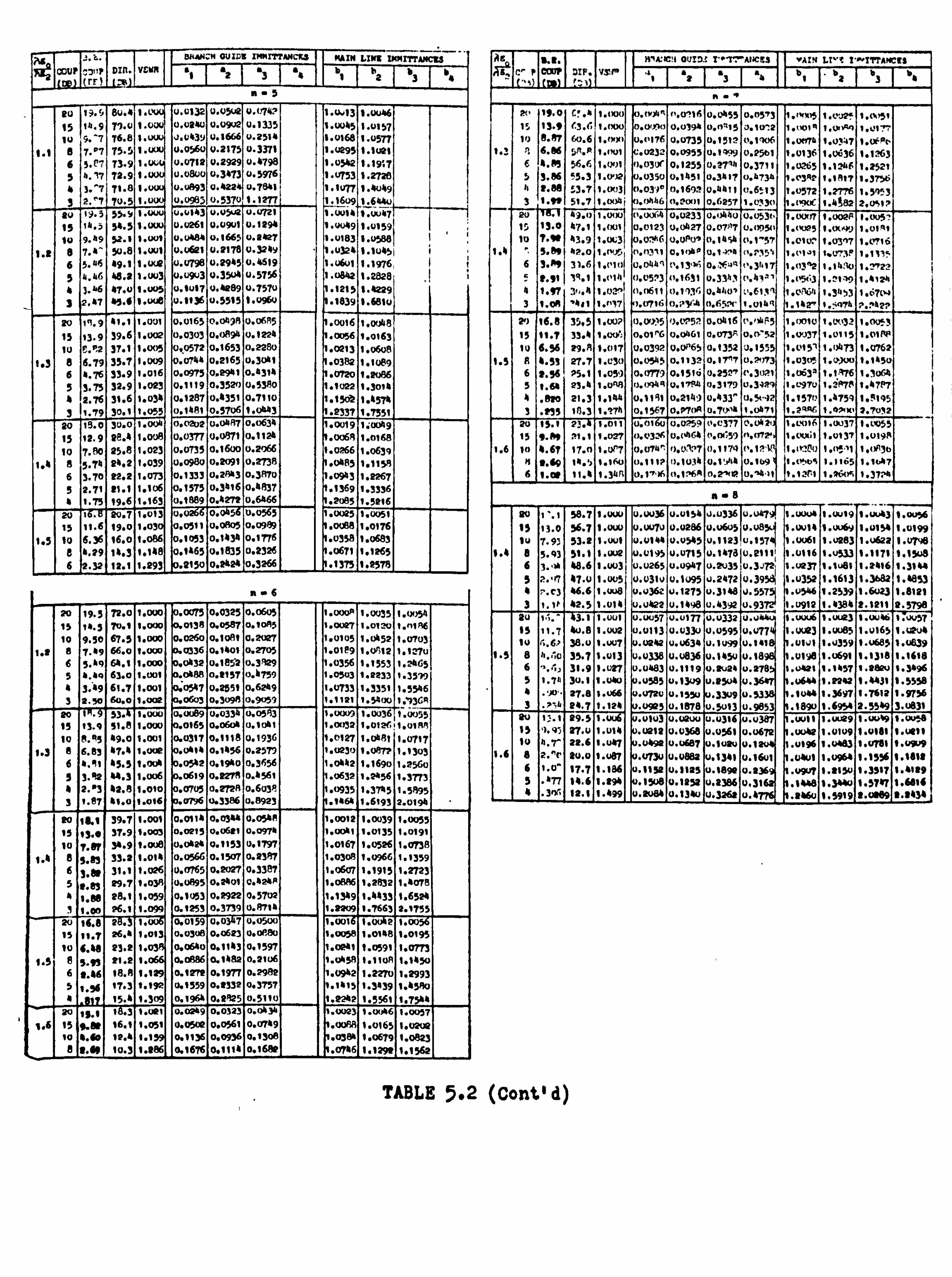
M BNANDN OUID6 Imr? r$NC23 PAZ" LINZ DmrrrARM Li
COUt C71+T DIR. Y£1f11 ý1 ý2 ý3 ýº el ý y , 2 3 º
nýS
ou 19.5 8u. 8 1. L 0.0132 0.0502 0.114 1.0.13 1.0086 15 18.9 77.0 1.000 0.0280 0.0902 0.1335 1. ou45 I. o157 1u 9. -7 76.8 I. uuu J. 0839 0.1666 0.2514 1.0168 1.0577
1.1 6 7. °7 75.5 -uuu 0.0560 0.2175 0.3371 1.0295 1.1021 6 5. (7 73.9 1. ouq 0.0712 0.2929 0.8798 1.0542 1.1957
4.17 72.9 1.00 0.0800 0.3473 0.5976 1.0753 1.2728 3. ý7 71.8 t. uuu 0.0893 9.42241 0.7841 1.1077 1.4049
3 2. °7 70.5 I. u 0.0965 0.5370 1.1277 1.1659 1_6440 , to 19.3 55.9 I. 000 0.083 0.0502 0.0721 1.001$ 1.00$7
15 14.5 58.5 1.000 0.0261 0.0901 U. 1298 1.0049 1.0159 10 9.89 52.1 1.001 0.0488 0.1665 0.2827 1.0183 8.0588 1
1.! 6 7.8 50.8 1.001 0.0621 0.2178 0.3249 1.03214 1.10451
6 5.46 89.1 1.002 0.0798 0.2945 0.4619 1.0601 1.1976, 5 4.46 46.2 1.003 0.0903 0.3508 0.5756 1.0842 1.2828
3.46 87.0 1.005 0.1017 0.4289 0.7570 . 1215 1.4229 3 2.87 85.0 l. ou8 0.1136 0.5515 1.0960 . 1839 1.6810
20 11.9 41.1 1.001 0.0165 0.0428 0.0685 . 0016 8.0008 15 13.9 39.6 1.002 0.0303 0.0894 0.1224 . 0056 1.0163
tu 6.: 2 37.1 1.005 0.0572 0.1653 0.2280 1.0213 1.0608 1.3 8 6.79 35.7 1,009 0.0744 0.2165 0.3041 . 0382 1.1089
6 4.76 33.9 1.016 0.0975 0.2941 0.8318 . 0720 1.2086 5 3.75 32.9 1.023 0.1119 0.3520 0.5380 1.1022 1.3010 4 2.76 31.6 1.034 0.1287 0.4351 0.7110 1.1503 1.4574 3 1.79 30.1 1.0" 0.1481 0.5706 1.0"3 1.2337 1.7351
20 15.0 30.0 1.004 0.0202 0.0487 0.0634 1.0019 1.0049 15 12.9 28.4 1.008 0.0377 0.09'/1 0.1124 . 0068 1.0168
10 7.80 25.8 1.023 0.0735 0.1600 0.2066 1.0266 1.0639 1.4 8 5.74 28.2 1.039 0.0980 0.2091 0.2738 . 0485 1.11-58
6 3.70 22.2 8.073 0.1333 0.2883 0.3870 1.0943 1.2267
5 2.71 21.1 1.106 0.1575 0.3416 0.4837 . 1369 1.3336 º 1.75 19.6 1.163 0.1889 0.4272 0.6466 . 2085 1.5216
20 1. 20.7 1.013 0.02615 0.0456 0.0 565 1.0x25 1.0051 IS It. 6 19.0 1.03 0.0511 0.0205 0.0989 . 0066 1.0176
1.5 tu 6.36 16.0 1.086 0.1053 0.1838 0.1776 , 0358 1.0683 6 1.29 18.3 1.148 0.1865 0.1835 0.2326 . 0671 1.1265 6 . 32 12.1 1.297 . 2150 0.2428 0.3266 . 1375 1.2578
n. e
20 19.5 72.0 1.000 . 0075 0.0325 0.0605 1.00op 1.0035 1.00556 15 14.5 70.1 1.000 0138 0.0587 0.1085 1.0027 1.0120 t. n186
10 9.50 67.5 1.000 0.0260 0.1081 0.20¢7 1.0105 1.0852 1.0703 1.! 8 7.89 66.0 1.000 0336 0.1401 0.2705 1.0189 I. oI2 1.1270
6 5.49 68.1 1.000 . 0432 0.1852 0.3929 1.0356 1.1553 1.2465 5 4.40 63.0 1.001 0888 0.2157 0. M759 1.0503 1.2233 1.3579 º 3. *9 61.7 1.001 0547 0.2551 0.6249 1.0733 1.3351 1.5546 3 2.50 60.0 1.002 0603 0.3098 0.9089 1.1121 1.5400 1. '9369
20 1 53. 1.000 o. 0ue9 0.03]4 0.0583 1.0009 1.0036i l. i1055 IS 13.9 S1.8 1.000 0165 o. 0604 0.1041 1.0902 1.01261 1.0189
10 8.95 49.0 1.001 0.0317 0.1118 0.1936 1.0127 1.0881 1.0717 1.3 8 6.83 47.4 1.08E . 0414 0.1456 0.2579 1.0230 1.0872 1.1303
6 4.91 45.5 1.004 . 0542 0.1940 0.3(556 1.0882 1.1690 1.2560 S 3.92 44.3 1.006 0619 0.2278 o. 4561 . 0632 1.2456 1.3773 4 2.03 42.8 1.010 . 0705 0.2728 0.6038 1.0935 1.3745 1.5895 3 1.87 41.0 t. o16 . 0796 0.3386 0.8923 . 1464 1.6,93 2.0194
20 10.1 39.7 1.001 0.0114 0.03* 0.0548 1.0012 1.0039 1.0055 13 13.0 37.9 1.003 0.0215 0.0621 0.0974 1.00 1 1.0135 1.0191 l0 7, A 34.9 1.008 0.0424 0.1153 0.1797 1.0167 1.0526 1.0738
1,4 8 5,83 33.2 1.014 0.0566 0.1507 0.2387 1.0308 1.0966 1.1359 6 3.01 31.1 1.026 0.0765 0.2027 0.3387 1.0607 1.1915 1.2723 5 1 83 29.7 1.038 0.01195 0.2401 0.8241 1. o$86 1.2832 1.8078
º 1,80 28.1 1.059 0.1053 0.2922 0.5702 1.1349 1.4433 1.6524 3 1.00 26.1 1.099 0.1253 0.3739 0.8714 1.2'209 1.7663 2.1755
20 16.6 2. 1. 060159 0. o 7 0.0500 1.001 1.2 1. is 11.7 26.4 1.013 0.0308 0.0623 O. OP80 1.0058 1.0148 1.0195 1o 6.48 23.2 1.03 0.0640 0.1143 0.1597 1.0241 1.0591 1.0773
1. S 6 S. 9! 21.2 1. 0.0886 0.1482 0.2106 1.0458 1.1108 1.1450 6 9.46 18.8 1.129 0.1272 0.1977 0.2982 1.0942 1.2270 1.2993 5 1,96 17.3 1.192 0.1559 0.2332 0.3757 1.1415 1.3439 1.4580 4 15.4 1.309 0.1964 0.2825 0.5110 1.2242 1.5561 1.75414
12.1 1 .] 1.021 0.0249 0.0]23 0.0530. 1.0023 1.0946 1.0087
j. 6 IS 9.85 16.1 1,051 0.05112 0.0561 0.07149 . 00ßf4 1.0165 1.15202 10 4,60 12,4 1.1 0.1136 0.09]6 0.1SOB . 0384 1.0679 1.0823
e ý. 6! 10.3 1.286 0.1676 alto 0.1652 . 0746 1.1291 1.1562
1ý6 1 M. H9A: 1011 OUIDS I'°'I'TAIJC63 vAI1 LP'i I'-ITrANCts , A8, C; P Cm DSF" YSJ" ") a 4 0 O I. b 11
i 12 3 4 4 t 3
n. ý
2n 19.0 f. ', 4 t. txro , txyl". rw16 u W55 0.0573 '"'Aj 1 I, r02ý Q1j1 15 13.9 (3"G, i. f)t)U 0,0990 0,0394 0.0115 0.10': 2
: 1.1.014 1, (x84 1, W
10 9.87 60.6 1. o, e 0.11176 0,0735 G. 1512 0.1906 1,0074 1.0347 I. 04"P0 14 11 6.86 58, P 1.001 . 0232 0.0955 0.1999 0.2561 1.0136 1.0636 1.1263
6 5.85 56.6 1"twl 0,030( 0.1255 0.2795 0.3711 1.02265 1.1346 1.2521 5 3.86 55.3 1"tr)2 , 0350 0,1451 0,3417 0.4734 . 03112 1.1817 1.3756 4 $$$ 53.7 1.013 0,0390 0.1692 0.4411 0.6513 1.0572 1,27% 1,5957 3 1.09 51.7 1. txY1j ). 01146 o. 9pt1 0.6257 1,0930 L. tgoC 1.4682 2.001?
211 18.1 49,0 1. IN)U 008 0.0233 0. U4hu U. u53t, 1, OOtq I, U02A I OUS'- 15 1 13.0 47.1 1,101
: 0,0123 0.0427 0.0709 0.0954) l. 0u25 LOl"MJ 00/
fu 7.98 43.9 1. (X3 0.07'6 0,4)20+ 0.1454 0,1'57 1.0107 1.0397 1.0/16 1.11 '" 5.59 112.0 I. mil" 0,01211 0.1n4ß U. 1"IP4 n.; 35" t, OWI t. U'! 38 1"I17
6 3.88 31.6 i, tgo 0,0441 0,13' 13,16 0.364) 11,34171 1,03^2 1.14,90 1.9722 9. I 54,1 1.014 11,05? 3 41.1631 0.3351 11.412, 1.0543 1.91)9 1,4124
4 1.97 3ý. "4 1.027 1(. 9611 0.1934 0.440+ 0.6199 1.096'4 1,3453 1.6709 3 1.09 '411 1"097 ). 0716 0,27(. & 1 0.65N. ' 1,0149 1.142' 1. "4Mh P. 042?
29 16.8 35.5 1,00? 0,0y>. 15 1). 0959 0.0416 (' , 0583 1.0010 1.01*32 1.0053 15 11.7 33.4 ': Q(4, 0,01"G 0,0461 0,0738 O, o'S2 1.0037 1.0115 1,0188
10 6.56 29.8 1.017 0.0392 0"x865 0.1352 0.1555 1.015' 1,0473 1,0762 1.5 8 4.53 27.7 1.030 0,0545 0.1132 0.1717 0.2073 1,0306 1,01)00 1.1450
6 2.56 25.1 1.059 0.0779 0.1516 0.252'1 (". 3021 1.063° 1,1"1176 1.9064 5 1.64 23.4 I, Una 0.00411 0.1784 0.3179 0.3429 1.0970 1.2878 4,47117 4
. 810 21.3 1,144 0.1191 0.2149 0.433° O, S. "92 1.1570 1,5759 1,9195 3 . 935 15.3 1.? 711 0.1567 0.27(5 0.70* 1.0571 1.2Q84 1.112(10 2.7012
20 15.1 23. (. (11 0,01 0. .' O, 0377 0,0121 l. LV)16 1.9037 1"11)55
15 9.89 21.1 1.027 0,0326 U. 1.16i ('. 0659 latn2' 1.1.16) 1.0137 1.0198
1.6 10 4.67 17.0 1.087 0.074"" 0.0127 0.1170 0,12" 1.11250 1.0511 1,9630 A 1.69 14.5 1.160 0.1112 0.1034 0.1514 0,149 l, tnuti 1.1165 1.1W7 6 1.0! 11.4 1.348 (). 1'^16 0.12611 0.2'"4. 0. '69 4 1,1 28 1 1,111x09 1,3724
p. 8
20 11.1 58.7 1.100 U. UU36 0.0154 0.0336 0.011'( 1.0004 1.0019 1.0413 1.0056
15 13.0 56.7 1,04)0 0"04)70 0.0286 0.0605 0"V8yuý 1.0015 1.0069 1.0154 1.0199 SU 7.9; 53.2 1"001 0,0144 u. 015 0.1123 4), 1.5711 1.0061 1.0283 1.0622 1.07'18
1.4 8 5.43 51.1 1.1102 0.0195 0.0715 0,1478 0.2111 1.0116 1.05 1.1171 1.154)8 6 3 ">11 48.6 1.1103 0.0265 0.0947 0.2035 0.3,172 1.0237 I. 1u81 1,2416 1.3144 . I 5 2.117 47.0 1.005 0.0310 0.1095 0.2472 0.3954 1.0352 1.1613 1.3682 1.1853 4 7. C3 46.6 1.1108 0.0362 0.1275 0.3148 0.55751 . 0546 1.2539 1.6023 1.8121 3 1.1) 42-51 1-014 0.0122 0.11198 0.4392 0.93721 1.0912 11-43819 12-1211 2.5796
20 1";. ' 3.1 1.001 u. uu57 0.0177 0.0332 4). o t. Uuu6 1.00¢3 0.00411 1-OV57 15 11.7 40.8 1.002 0.0113 0.0330 0.0595 0.4)77 1.0.53 1,0085 1.0165 1.0204 tu 6.61 38.0 1.007 . 0242 u. 1634 0.1099 0.141 , 0101 1.9359 1.0685 1.0839
1,5 8 4,8.0 35.7 1.013 00336 U. U836 0.1550 U. 1898 1.0190 1.0691 1.1318 1.1616 6 1.4' 31.9 1.027 0.0583 0.1119 0.2024 0.278 1.0121 1.1457 1.2920 1.3496 5 1.71 30.1 1.040 "0585 0.1309 0.2504 u. . u688 1.2242 1.4431 1.5558 4 . 90 37.8 1.066 0,0720 0.1550 . 3309 0.5338 . 1015 1.3697 1.7612 1.9756 3 . 214 24.7 1.124 . 0925 0.1878 0.5013 0.9653 . 1890 1.6954 2.5549 3.0831
YO 1: "1 29.5 1. . 0103 4"02W 0.0316 0.0387 , wll 4.0029 1,111019 1.0+59 15 9.93 27.0 1.015 . 0212 0.0368 0.0561 0.06'2 . 00112 1.0109 1.11181 1,0! 11 10 44.7' 12.6 1.017 , 0192 u"U687 0.10111 0.1 1.0196 1.0483 1.0/61 I, U¢19
1.6 8 2. ̂ r 20.0 1.087 , u'º3u u, u882 0,1341 0.1601 . 084)1 1.0964 1.1556 1.1611 6 1.0" 17.7 1.186 11.1152 0.1125 0.1890 0.236 . u9j7 1.2150 1.3517 1.4129 5 . 477 11.6 1,295 , 1508 0.1257 0.2386 0,3162 , 1448 1.3180 1.5747 1.6616 4 Anrr 12.1 1.499 0,2088 0.1340 U, 326* 0.4 . 2460 1,3919 2.17189 11.71431
TABLE 5.2 (Cont'd)
144
Performance curves for 3 dB Butterworth couplers having
3 to 9 branches are shown in Fig. 5.8. In these curves VSWR
has been plotted, and the directivity shows similar maximally
flat behaviour. The performance of a3 dB coupler having
eight branch guides analyzed from previously published re-
aults(3) is also shown for comparison as the dotted line in
Fig-5.8. It has been shown by analysis that the reason that
the latter is inferior to the present result for n&-8 is that
the zeros of the F function (see Eq. (5.52)) of this previous
result are clustered about the midband frequency rather than
being exactly coincident with it.
The performance of Chebyshev designs is displayed in
Figs-5.9 through 5.12 for a large number of center frequency
coupling values and for various numbers of branch guides.
Each figure represents a case of constant bandwidth. The
curves show the maximum passband VSWR and the minimum pass-
band directivity for a given number of branch guides as the
center frequency coupling is varied. The latter values are
indicated in decibels by the labelled points on the curves.
These figures present an overall picture of performance and
are useful in selecting a design for a given specification.
It is evident that it is now feasible to design sym-
metrical branch-guide couplers to give excellent VSWR and
directivity over much broader bandwidths than hitherto thought

iw
1. c
VSWR RESULTS OF SYNTHESIS
ýýý Vr11 %1.1o% IC rbr--anl iii . (2*) Cr1b 0 dr, 1 llr'Lim=
i
1.
I
I
1
Abo 012
71 6eo
Fig. 5.8. -VSWR as a function of frequency for Butterworth branch-guide couplers.
1. o 1.1 1.2 1.5 1.4
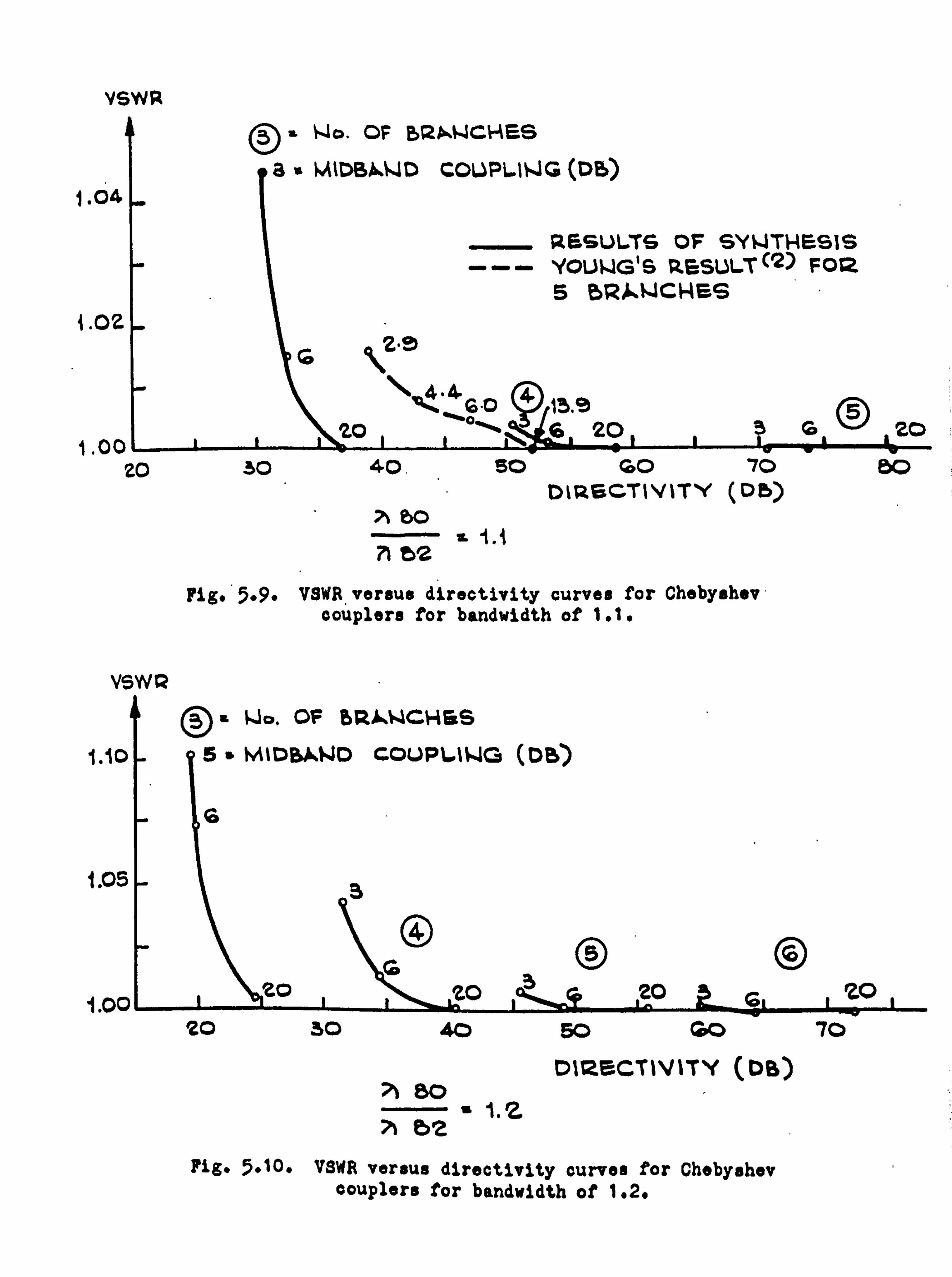
VSWR
O- No. OF bRAWCHES
3" N11DBA04D COL PLNG (DB)
1.04
RESULTS OF SYt4THESIS --- YOUIJG' S RESULT(2) FOQ
5 BRi"t4CHES 4.02
6 ý29 ý 4.4 4. j5 9
2O 6 210 G 20 1.00
20 50 40. SO GO 76 50 DIRSCTIVITY (Db)
TBO -s1.1 71 fl2
Fig. 5.9" VSWR versus directivity curves for Chebyshev, couplers for bandwidth of 1.1.
VSWQ 3O i {. lo. OF ßRi. WCHr. S
1.10 5" MIDBºNO COUPL. II. IG (OB)
6
1.05 3
6
i . 00 2O 2O 3 20 6 2O
20 30 40 50 GO 70
DIRECTIVITY (DB) 71 80
s 1.2 T 02
Fig. 5.10. VSWR versus directivity curves for Chebyshev couplers for bandwidth of 1.2.

vswa 1.10
I
0 Qa
0 ,3
10 ?A 30 4.0 b0 GO
7%50 DI RMGTI'I ITY (Da)
;ý 82 s 1.4 '
Fig. 5.11. VSWR versus directivity curves for Chebyshev couplers for bandwidth of 1.4.
vsw R
,. z ©o 4r. _A
1.1
i. 0 I 10 15
O FJo. -OF bRM CHES
15 43
MIDBA. WD COUPLIIJG (D6)
®" Flo. OF bQÄWCHES
06 " MIDENÄW D COUPLING (DB)
8
20 25 30
D1R6GTt TY (DB) ýº80
ýº a2
Fig. 5.12. VSWR versus directivity curves for Chebyshev couplers for bandwidth of 1.6.

145
possible. A comparison with previous Chebyshev designs(3)
is shown as the dotted curve in Fig. 5.9. It is seen that
here an even greater improvement is attained than in the
Butterworth case.
1.4.2 The Asymmetrical Case(lo).
If the output resistance RL is allowed to be different
from the source resistance R8, then it has been seen previously
(i. e., in the numerical example) that an asymmetrical coupler
will result. This device is therefore both a branch-guide
directional coupler and impedance transformer.
Such an impedance transformer with loose coupling might
find application in antenna design work and other fields.
Accordingly, Table 5.3 gives the values of branch and main
line immittances for the Butterworth specification for 3 to 5
branches, coupling from 40 to 10 dB, and R (the output to in-
put conductance or resistance ratio) from 2 to 10. The band-
width corresponding to the frequency at which the directivity
falls to 20 dB is given for each case and also the coupling
and VSWR at this point. Similarly Table 5.4 gives design
information for Chebyshev characteristics for 3 to 5 branches.
The maximum ripple VSWR and worst ripple directivity are
given, as well as the band edge coupling (B. E. C. ), for
bandwidths of 1.1 and 1.2. As before, the immittances are
admittances for a stripline realization (normalized to 1 mho)

ELEMENT VALUES FOR BUTTERWORTH BRANCH-GUIDE COUPLER-TRANSFORMERS OF RESISTANCE RATIO R AND COUPLING C (IN DB) FOR N-3 TO 5 BRANCHES
B. E. i" 8. E. BR NCN GUIDE IMMITTANCES MAIN LINE IMMI ANCES
R C C A IX- VSWR a1 a2 &3 1 a4 a5 I b1 b2 b b4
n 40 39.55 1.20 1.04 0.0055 0.0150 0.0101 1.1067 1.3555
1.5 30 29.56 1.20 1.04 0.0175 0.0475 0.0319 1.1073 1.3562
20 19.58 1.18 1.04 0.0559 0.1518 0.1005 1.1129 1.3639 lU .6 1.1 1.06 9,1661 0.5442 0,2 1.1818 1.41 40 39.55 1.20 1.07 0.0059 0.0200 0.0165 1.1893 1.6819
2 30 29.57 1.20 1.07 0.0187 U. U633 U. U521 1.190k) 1.6832
20 19.60 1.18 1.06 0.0603 0.2032 u. 1637 1.1978 1.6966 tU ,6 1,14 1.08 0 . 2062 0.66 0.2 1. ou4 1,8640 40 39.59 1.20 1.18 0.0070 0.0500 0.0768 1.4956 3.3445
5 30 29.62 1.18 1.16 0.0227 0.1587 0.2406 1.4977 3.3519 20 19.69 1.15 1.11 0.0770 0.5218 0.7487 1.5214 3.4296 tu .8 1.10 14 U28 3.0130 2.6933 1,9790 4.8146 40 39-73 1.16 1.20 . 0078 0.1001 0.2382 1.7788 5.6264 1
10
1
30
1
29.70 1.16 1.20 0.0261 0.3189 0.7421 1.7836 5.6538 20 19-78 1,12 1,12 U, U 46 1.0959 2.3143 1.8416 0
n-4 4U 38.96 1.30 1.04 . 0026 0.0096 0.0130 0.0053 1.0521 1.2248 1.4259
t. 5 3U 28.97 1.30 1.04 0.0084 U. 03U5 0.0412 U. U168 1.0523 1.2257 1.4264
20 19.03 1.28 1.04 . 0271 0.0975 . 1.3o6 0.0529 1.0555 1.2346 1.4314 to 1.24 1.06 0.0913 o. 3448 2 ,4 0,168 1.0973 1.3507 1.4944 40 38.96 1.30 1.07 0.0027 0.. 0115 0.0192 0.0090 ' 1.0907 1.4144 1.8338
2 3u 28.99 1.30 1.07 0.0087 0.0364 0.0607 0.0283 1.0911 1.4157 1.8347 20 19.07 1.27 1.06 0.0286 0.1172 0.1925 0.0886 1.0953 1.4296 1.8439 10 .2 1.22 1.08 UU8 U. 4 6 U, 00 0.2778. 1.1 1.6244 1.9645. 40 39.02 1.30 1.18 0.0029 0.0197 0.0649 0,0462 1.2253 2.2366 4.0815
5 30 29.09 1.28 1.15 U. oo96 0.0632 0.2044 0.1437 1.2263 2.2419 4.0876 20 19.25 1.24 1.10 U. 0344 0.2126 o, 6561 0.4361 1.2380 2.3010 4.1518
IU 9.57 ,1 1.12 0.1299 1.1921 1.5944 1.3379 1.48 3.6672 5.3055 4c 39.25 1.26 1.20 0.0030 0.0293 0.1595 0.1535 1.3411 3.1639 7.4606
10 30 29.21 1.26 1.19 o. 01U4 0.0959 0,5022 U. 47U9 1.3432 3.1791 7.4865 2U 1 .4 1.20 1.10 (). 0415 W. 3447. 1.66841 1.39741 - 1.17u3- 3.363(; - 7,7645-
_ n ý'. 4u 38.36 1.38 1.04 0,0013 u. uo58 0.0112 0.0096 (1.0027 1.0257 1.1352 1.3215 1.4624
1.5 3U 28,39 1.37 1.04 0.0041 0.0184 0,0354 0.0303 U. UU86 1.0259 1.1358 1.3224 1.4627
2. 18,47 1.35 1.04 0.0136 0.0593 0.1123 0.0955 0.0275 1.0276 1.1428 1.3311 1.4656 to 8.72 1-10 1-07 U. U4 1 0,2(-61 0.401 0.3203 U. U881 1.0516 1.2 1.4495 1.5038 4U 38.37 1.38 1.07 0.0013 0. UU64 U. U148 0.0151 0.0047 1.0445 1.2422 1.6104 1.9150
2 30 28.41 1.37 1.07 . 0042 0,02-5 U. U469 0.0477 0 . 0148 1.0447 1.2431 1.6118 1.9155 2u 18.53 1.34 t. o6 0.0142 0.0667 0.1494 0.1497 u . 467 1.0469 1.2533 1.6267 1.9209 1u 8.84 1.29 1.08 U, °a° 0,24 t 10.5679 0.5129 0,14 i u8t6 1.4o66. 1,6417 1.9961 4u 38.44 1.37 1.18 0.0u13 0.0086 c. 0356 0,0624 0.0257 1.1081 1.6572 3.0185 4.5130
5 3u 28.54 1.35 1.14 0.0045 0.0283 0.1129 0.1948 0.0796 1.1085 1.66u1 3.0258 4.5169 2u 18.79 1.30 1.09 0,0171 0.0989 0.3709 c. 6c66 0.2396 1.1146 1.6953 3.1069 4.5589 lo (, 1 1.? 2 1.12 0.06 58 U, 4 U 2.4660 2,6'2 c. 6 1,? 88 2.6110 5. t7 6 ß 40 38.72 1.34 1.20 0.0013 0,1) 1.7 0.0677 0. '1760 U. o891 1.1614 2.0658 4.8451 8.6131
tu 3u 28.72 1.32 1.13 0.. 0049 0.0364 0.2168 0.5455 0.2712 1.1624 2.0732 4.8703 8.6312 20 t. 1 . 25 1, (. 1' 0,2, 'u 1 U4 755 1.71Q U. 8 1.1764 m698 16 8.8264
TABLE. .3

ELEMENT VALUES FOR CHEBYSHEV BRANCH-GUIDE COUPLER-TRANSFORMERS WITH A BANDWIDTH OF 1.1, RESISTANCE RATIO F. AND COUPLING C (IN DB) FOR N-3 TO 9'BRANCHES
R C B. E. DIR V$WR BRANCH GUIDE IMMITTANCES MAIN LINE IMMITTANCES C (DB) al a2 a3 a4 a5 bl b2 b3 b4
n-3 40 39.89 37.8 1.009 0.0060 0.0197 U. U167 1.1919 1.6782
2 30 29.89 37.3 1.009 0.0190 0.0625 0.0527 1.1927 1.6795 20 19.88 35.7 1.009 0.0614 0.2000 0.1659 1.2uo6 1.6930 tv 9.44 31.5 1.019 0.2122 1.7492 0.5447 1.3057 1.8626 40 39.9 37. t. U23 0.0071 0. v 92 0.077 1.5039 3.3259
5 30 29.88 36.1 1.023 0.0232 0.1559 0.2431 1.5061 3.3333 20 19.86 32.7 1.024 0.0792 0.51v6 0.7590 1.5304 3.4111 iu 9.81 25.3 t. v69 0.3183 2.9233 2.7985 2.0129 4.8272
39.89 36.8 1.036 0.008v 0.0979 0.2403 1.7946 5.5768 10 30 29.88 34.4 1.036
1 0.0269 0,3114 0.7497 1.7996 5.6v4v 20 19.84 29.0 1.041 1 0.0984 1.0644 2.3511 1.8599 5.9005
n-4 v 39-89 59.9 1.001 0.002 0.0114 0.0191 v. v092 1.0925 1.4144 1.830
2 30 29.89 59.2 1.001 0.0089 0.0362 0.0602 0.0288 1.0929 1.4157 1.8317
1
20
1
19.88 57.2 1.001 0.0292 0.1165 0.1908 0.0904 1.0972 1.4296 1.841u 10 9.61 52.0 1.002 0.1022 0.4335 0.6927 0.2856 1.1596 1.6255 1.9644 4v 39.89 59.4 1.002 0.0029 0.0196 0.0642 0.0470 1.2302 2.2366 4.0653
5 30 29.89 57.7 1.002 0.0098 0.0630 0.2019 0.1461 1.2312 2.2419 4.0714 20 19.87 53.6 1.002 0. J354 0.2117 0.6473 0.4449 1.2432 2.3011 4.1364 tv 9.85 44.6 '1.006 2.1372 1.1904 3.5560 1.3913 1.5072 3.6871 5.3273 40 39.89 58.5 1.003 0.0031 0.0292 0.1571 0.1559 1.3492 3.1639 7.4157
10 3u 29.88 55.6 1.003 u. vt08 0.0956 0.4944 0.4789 1.3514 3.1791 7.4417 20 19.86 49.2 1.003 0.0432 0.3434 1.6393 1.4281 1.3796 3.3637 7.7231
n-5 40 39.89 81.9 1.000 0. vv13 v. ov64 0.0147 0.0151 U. 0v48 1.0456 1.2435 1.6086 1.9129
2 30 29.89 81.1 1.000 0.0043 0.0205 0.0464 0.0475 0.0152 1.0458 1.2444 1.6100 1.9134 20 19.88 78.8 1.000 0.0146 0.0668 0.1479 0.1493 0.0479 1.0481 1.2547 1.6250 1.9190 IU 9.87 72.8 1.000 0.0530 0.2442 0.5609 0.5125 0.1508 1.0841 1.4097 1.8415 1.9965 4u 39.89 81.3 t. vvv 0.0014 0.0087 0.0352 0.0621 0.0263 1.1110 1.6615 3.0107 4.5011
5 30 29.89 79.4 1.000 0.0047 0.0285 0.1117 0.1937 0.0815 1.1115 1.6645 3.0180 4.5051 20 19.88 74.7 1.000 0.0177 0.0996 0.3666 0.6033 0.2461 1.1177 1.7000 3.0991 4.5480 10 9.86 64.3 1.001 0.0694 0.4982 2.4393 2.7803 0.7030 1.2694 2.6376 5.0967 5.3591 40 39.89 80.3 1.00v 0.0014 0.0107 0.0669 0.1746 0.0911 1.1660 2.0739 4.8262 8.5792
tu 30 29.88 77.0 1.000 0.0051 0.0367 0.2142 0.5410 0.2778 1.1670 2.0813 4.8514 8.5976 20 19.87 69.8 1.000 0.0221 0.141a 0.7449 1.7061 o. 8080 1.1816 2.1793 5.1506 8.7972
TABLE g. 4
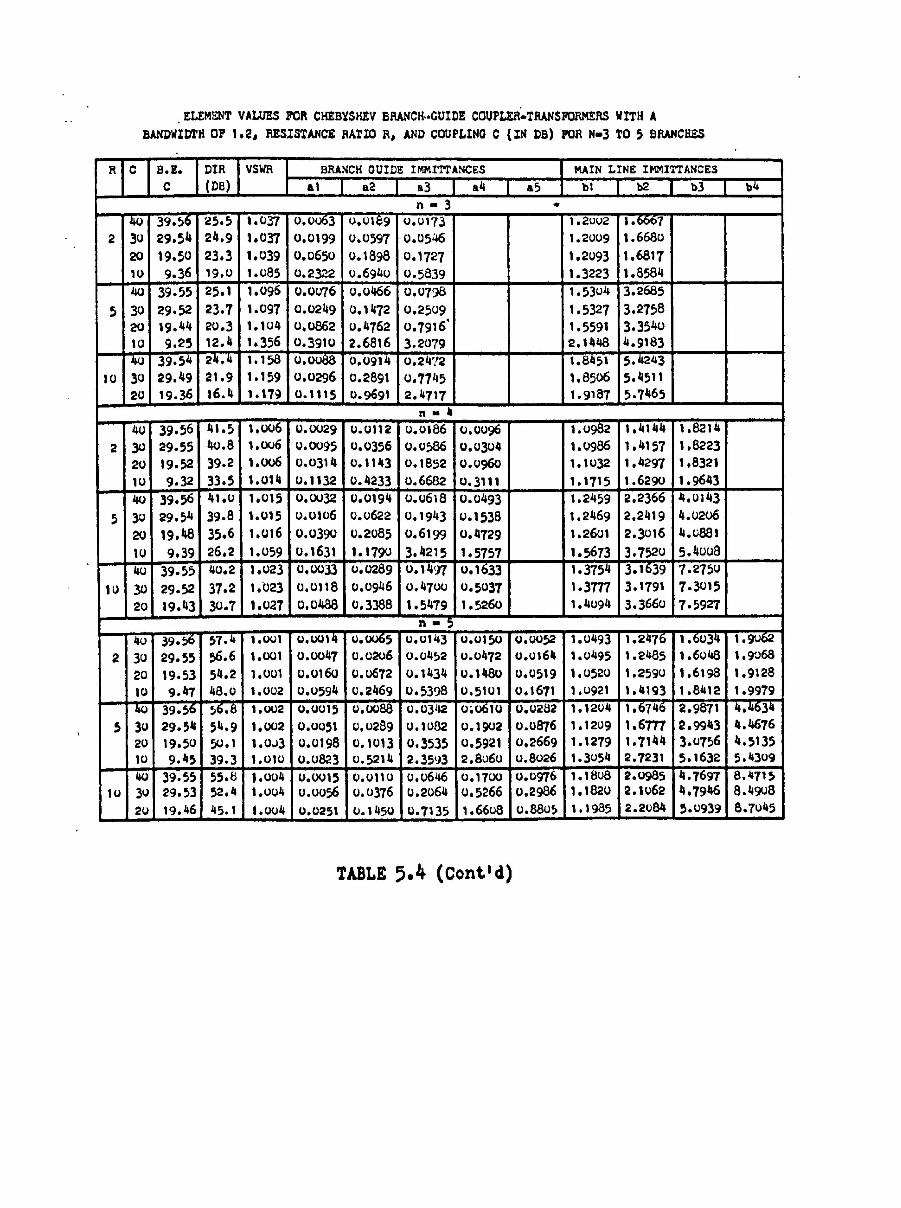
ELEMENT VALUES FOR CHEBYSHEV BRANCH. -GUIDE COUPLER-TRANSFORMERS WITH A
BANDWIDTH OF 1.2, RESISTANCE RATIO R, AND COUPLING 0 (IN DB) FOR N-3 TO 5 BRANCHES
RI C 8. E. DIR VSWR BRANCH GUIDE IMMITTANCES MAIN LINE IKMITTANCES C (DB) al a2 a3 a4 a5 bt b2 b3 b4
ný3 " 40 39.5 25.5 1.037 0.0063 0.01 9 0.0173 1.2002 1-6667
2 30 29.54 24.9 1.037 0.0199 0.0597 0.0546 1.2009 1.6680 1 1
20 19.50 23.3 1.039 0.0650 0.1898 0.1727 1.2093 1.6817 10 9.36 19.0 1.085 0.2322 0.6940 0.5839 1.3223 1.8584 40 39.55 25.1 1.096 0.0076 u. u466 0.0798 1.5304 3.2685
5 30 29.52 23.7 1.097 0.0249 0.1472 0.2509 1.5327 3.2758 20 19.44 20.3 1.104 0.0862 0.4762 0.7916" 1.5591 3.3540 10 9.25 12.4 1.356 0.3910 2.6816 3.2079 2.1448 4.9183
39.5 2. 1.158 0.00 0.0914 0.2472 1.8451 5.43 tv 30 29.49 21.9 1.159 0.0296 0.2891 0.7745 1.8506 5.4511
20 19.36 16.4 1.179 0.1115 u. 9691 2.4717 1.9187 5.7465 n- :1
40 39.56 41.5 1.006 0.0029 0.0112 u. 0186 0.0096 1.0982 1.4144 1.8214
2 30 29.55 4o. 8 1. W6 0.0095 0.0356 0.0586 0.0304 1.0986 1.4157 1.6223 20 19.52 39.2 1.006 0.0314 0.1143 0.1852 0.0960 1.1032 1.4297 1.8321
10 9.32 33.5 1.014 0.1132 0.4233 0.6682 0.3111 1.1715 1.6290 1.9643
40 39.56 41.0 1.015 0.0032 0.0194 0. u618 0.0493 1.2459 2.2366 4.0143
5 30 29.54 39.8 1.015 0.0106 0.0622 0.1943 0.1538 1.2469 2.2419 4.0206
20 19.48 35.6 1.016 0.0390 0.2085 0.6199 0.4729 1.2601 2.3016 4.0881 tu 9.39 26.2 1.059 0.1631 1.1790 3.4215 1.5757 1.5673 3.7520 5.4uU8 0 39.55 0.2 1.023 0.0033 0.0289 0.1497 0.1 33 1.3754 3.1 39 7.2750
10 30 29.52 37.2 1.023 0.0118 0.0946 0.4700 0.5037 1.3777 3.1791 7.3015 20 19.43 30.7 1.027 0.0488 0.3388 1.5479 1.5260 1.4094 3.3660 7.5927
n" 40 39. 7. '. out 0.001 0.5 0.0143 0.0150 0.0052 1.0493 1.2476 1.03 1.90
2 30 29.55 56.6 1.001 0.0047 0.0206 0.0452 0.0472 v. o164 1.0495 1.2485 1.6048 1.9068 20 19.53 54.2 1.001 0.0160 0.0672 0.1434 0.1480 0.0519 1.0520 1.2590 1.6198 1.9128
iv 9.47 48.0 1.002 0.0594 0.2469 0.5398 0.5101 0.1671 1.0921 1.4193 1.8412 1.9979
-r u, 5" 1.002 0.0015 v. W88 0.0342 0.0610 0.0282 1.1204 1-6746 2.9871 4.4634 5 30 29.54 54.9 1.002 0.0051 0.0289 0.1082 0.1902 0.0876 1.1209 1.6777 2.9943 4.4676
20 19.50 50.1 1.0., 3 0.0198 0.1013 0.3535 0.5921 0.2669 1.1279 1.7144 3.0756 4.5135 10 9.45 39.3 1.010 0.0823 0.5214 2.3593 2.8060 0.8026 1.3054 2.7231 5.1632 5.4309 40 39.55 55.8 ). uu4 0.0015 0.0110 u. u646 0.1700 0.0976 1.1808 2.0985 4.7697 8.4715
10 3u 29.53 52.4 1.004 0.0056 0.0376 0.2064 0.5266 0.2986 1.1820 2.1062 4.7946 8.4908
20 19.46 45.1 1. uu4 0.0251 0.1450 0.7135 1.6608 0.8805 1.1985 2.2084 5.0939 8.7045
TABLE 5.4 (Cont'd)
146
and the output conductance of the coupler-transformer is R
mhos. The dual is true for the waveguide case.
Another interesting application of the asymmetrical
coupler is in the design of hybrids, that is, 3 dB couplers.
In Table 5.5 hybrid designs are presented, with the idea
of maximizing bandwidth for a given (minimum) directivity
specification D over the band. In this case the computer
program was given a starting BW, from which it computed the
minimum directivity D1 over the band (after iterating to the
correct midband coupling value). If Dl did not agree with D
(to 8 place accuracy), the program modified BW and cycled re-
peatedly until Dn did agree with D. In Table 5.5, the
optimized bandwidth is listed as well as the maximum ripple
VSWR and the t L. C variation in coupling, I. e.,, the midband
coupling is 3.01$ AC dB, and the band edge coupling is
3-01-AC dB. It is hoped that these designs will prove
useful in stripline work. Accordingly, the ratio of element
values for any given design in Table 5.5 does not exceed 8.5.
All hybrid designs with five or more branches have been found
to exceed this limit. An interesting property to observe in
Table 5.5 is that for a fixed directivity, bandwidth increases
as R is reduced, although the element value ratio increases.
It was also found that as R is increased beyond unity the
bandwidth decreases, with the element value ratio again in-
creasing.
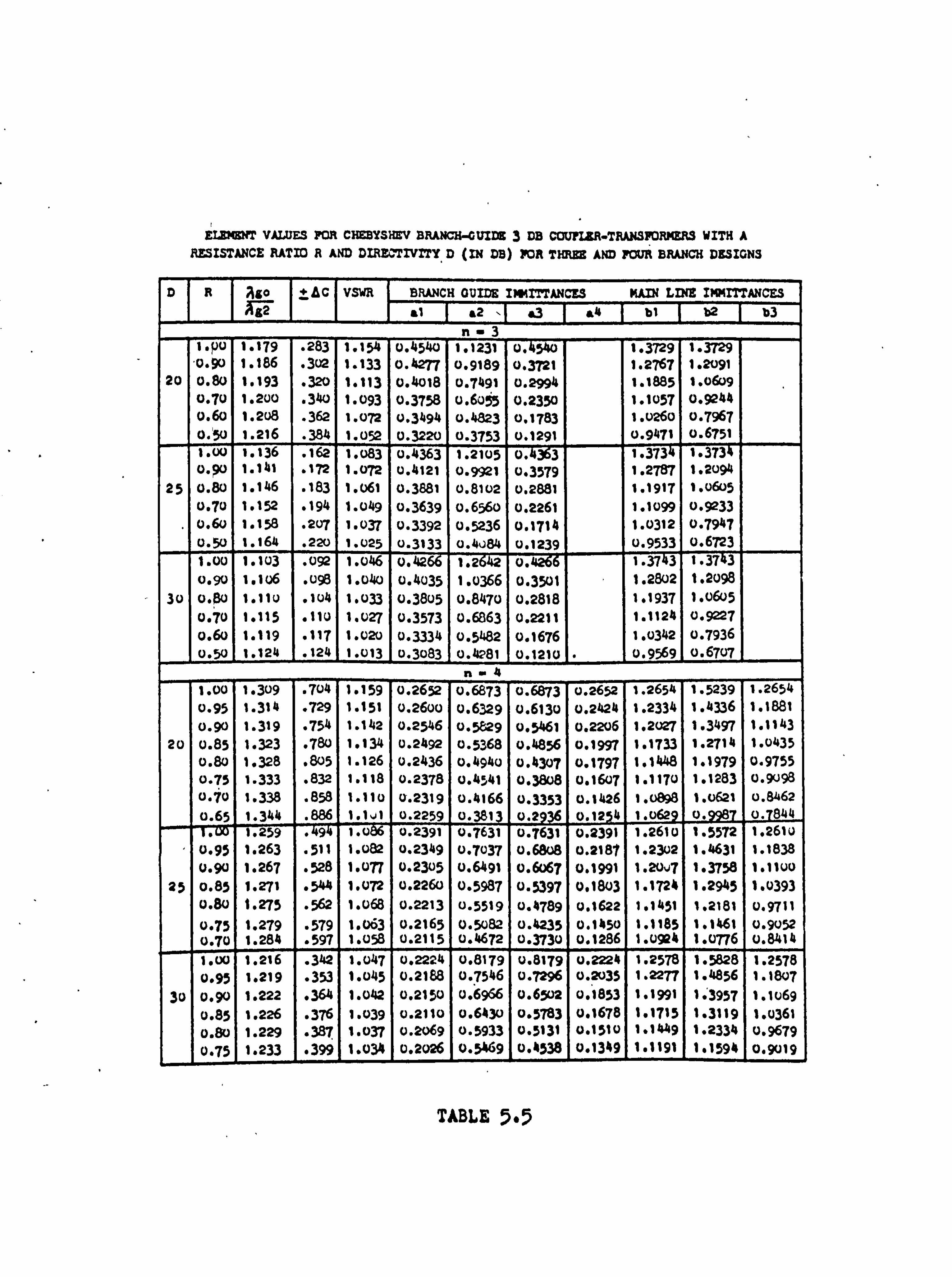
ELEMENT VALUES FOR CHEBYSHEV BRANCH-GUIDE 3 DB COUTIZR"TRANSHORMERS WITH A RESISTANCE RATIO R AND DI ECTIVITY D (IN DB) POE THREE AND FOUR BRANCH DESIGNS
D R Ago _AC VSWR BRANCH GUIDE IIMITTANCES MAIN LINE IPO4ITTANCES
&1 s2 s &3 a4 b1 b2 b3
n-3 t. po 1.179 . 283 1.154 0.4540 1.1231 0.540 1.3729 1.3729 "0.90 1.186 . 302 1.133 0.4277 0.9189 0.3721 1.2767 1.2091
20 0.80 1.193 . 320 1.113 0.4018 0.7491 0.2994 1.1885 1.0609
0.70 1.200 . 340 1.093 0.3758 0.6055 0.2350 1.1057 0.9244 0.60 1.208 . 362 1.072 0.3494 0.4823 0.1783 1.0260 0.7967 0.50 1.216 . 384 1.052 0.3220 0.3753 0.1291 0.9471 0.6751
1.0 1.136 . 162 1.083 0.4363 1.2105 0.4363 1.3734 1.373 0. q0 1.141 . 172 1.072 0.4121 0.9921 0.3579 1.2787 1.2094
25 0.80 1.146 . 183 1.061 0.3881 0.8102 0.2881 1.1917 1.0605
0.70 1.152 . 194 1.049 0.3639 0.6560 0.2261 1.1099 0.9233 U. 60 1.158 . 207 1.037 0.3392 0.5236 0.1714 1.0312 0.7947
0.50 1.164 . 220 1.025 0.3133 0.4084 0.1239 0.9533 0.6723 1. UO 1.103 . 092 1.046 0.426 1.2642 0. -4266 1.3743 1.3743 0.90 1.106 . 098 1.040 0.4035 1.0366 0.3501 1.2802 1.2098
30 0. $0 1.110 104 1.033 0.3805 0.8470 0.2818 1.1937 1.0605 0.70 1.115 . 110 1.027 0.3573 0.6863 0.2211 1.1124 0.9227
o. 60 1.119 . 117 1.020 0.3334 0.5482 0.1676 1.0342 0.7936 0.50 1.124 . 124 1.013 0.3083 0.4281 0.1210 . 0.9569 0.6707
n. 4
1.00 1.309 . 704 1.159 0.2652 0.6873 0.6873 0.2652 1.2654 1.5239 1.2654 0.95 1.314 "729 1.151 0.2600 0.6329 0.6130 0.2424 1.2334 1.4336 1.1881 0.90 1.319 . 754 1.142 0.2546 0.5829 o. 5461 0.2206 1.2027 1.3497 1.1143
20 0.85 1.323 . 780 1.134 0.2492 0.5368 0.4856 0.1997 1.1733 1.2714 1.0435 0.80 1.328 . 805 1.126 0.2436 0.4940 0.4307 0.1797 1.1448 1.1979 0.9755 0.75 1.333 . 832 1.118 0.2378 0.4541 0.3808 0.1607 1.1170 1.1283 0.9098 0.70 1.338 . 858 1.110 0.2319 0.4166 0.3353 0.1426 1.0898 1.0621 0.8462 0.65 1.344 . 886 1.1.1 0.2259 0.381 0-2936 .
0.1254 1.0629 0.9987 0.7844 I-UO 1.259 . 494 1.086 0.2391 0.7631 0.7631 0.2391 1.2610 1.5572 1.2610 0.95 1.263 . 511 1.082 0.2349 0.7037 D. 68o8 0.2181 1.2302 1.4631 1.1838
0.90 1.267 "528 1.077 0.2305 0.6491 0.6067 0.1991 1.207 1.3758 1.1100 25 o. 85 1.271 . 544 1.072 0.2260 0.5987 0.5397 0.1803 1.1724 1.2945 1.0393
o. 80 1.275 . 562 1.068 0.2213 0.5519 0.4789 0.1622 1.1451 1.2181 0.9711
0.75 1.279 . 579 1.063 0.2165 0.5082 0.4235 0.11150 1.1185 1.1461 0.9052 0.70 1.284 . 597 1.058 0.2115 0.4672 0.3730 0.1286 1.0924 1.0776 0.8414 1.00 1.216 . 342 1.047 0.2224 0.8179 0.8179 0.2224 1.2578 1.5828 1.2578
0.95 1.219 . 353 1.045 0.2188 0.7546 0.7296 0.2035 1.2277 1.4856 1.1807 30 0.90 1.222 . 364 1.042 0.2150 0.6966 0.6502 0.1853 1.1991 1.3957 1.1069
0.85 1.226 . 376 1.039 0.2110 0.6430 0.5783 0.1678 1.1715 1.3119 1.0361 o. So 1.229 . 387 1.037 0.2069 o. 5933 0.5131 0.1510 1.1449 1.2334 0.9679 0.75 1.233 . 399 1.034 0.2026 0.5469 0.4538 0.1349 1.1191 1.1594 0.9019
TABLE 5.5
147
A practical use for Table 5.5 is in the design of hybride
p for balanced transistor microwave am lifters(14) The ampli-
fier is designed to give the same amplification as one of the
transistors by itself. There are practical advantages to
using the circuit in Fig. 5.13 instead of a single ended design,
however. At present, manufacturing techniques for microwave
transistors yield devices having substantial performance dif-
ferences, that is, a high degree of repeatability has not yet
been achieved. This is a serious drawback in single ended
designs; each amplifier must be "custom made" to obtain the
beat performance from the transistor chosen for that amplifier.
In the balanced amplifier, however, it is only necessary to
use a pair of transistors having approximately the same elec-
trical performance. Therefore nearly all of the microwave
transistors from a batch production run may be paired and then
used in balanced amplifiers. It may also be shown(14) that
the balanced amplifier has a3 dB higher gain compression
compared with the single ended design and a9 dB improvement
in third order intermodulation. Furthermore, the couplers
in Fig-5-13 improve the input and output match to the tran-
sistors. For example, If the transistors each have an
input VSWR of 2.0, then the balanced amplifier (using
symmetric hybrids) can be designed to have a VSWR of 1.07
over the band of operation(14).
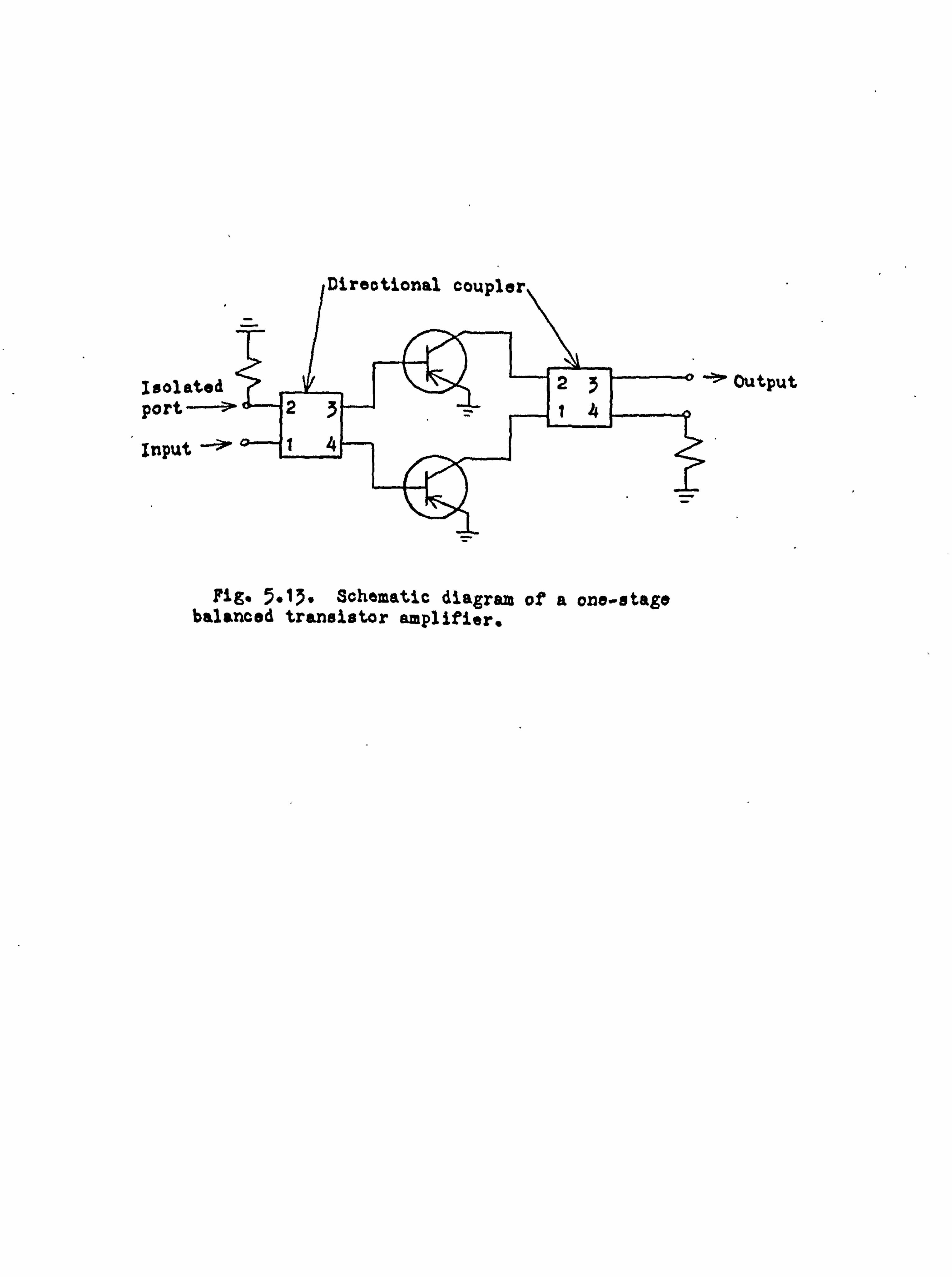
Isolated port --ý
Input --ý"
''ý, Output
Fig. 5.15. Schematic diagram of a one-stage balanced transistor amplifier.
148
A further improvement in the design of this structure
should be possible by using the asymmetric coupler-transformers
described above, for the following reasons:
1) The asymmetric hybrid has a larger bandwidth than
the corresponding symmetric one.
2) The asymmetric hybrid, acting as a transformer,
provides a better match between the input (or output)
line and the transistors.
Thus the asymmetric coupler-transformer is tailored to this
type of application.
.5 Experimental Results.
Several symmetric designs for Butterworth and Chebyshev
characteristics have been constructed both in X-band waveguide
and in stripline. Due account was taken of corrections to be
applied to the branch and main arm lengths and impedances due
to discontinuities as explained in Reference (15), which also
gives an example of the complete design procedure which was
employed. In the waveguide designs, each coupler was con-
structed in the form of a metal block with slots forming
the branch guides. The block was inserted between two wave-
guides having a section of one side of their broad walls,
equal to the length of the block, removed. A photograph of
this construction arrangement is shown in Fig-5-14. The
arrangement suffered from practical limitations, e. g., the
Fig. 5.14. Photograph of a waveguide branch-guide coupler.
149
difficulty of obtaining good contacts, and the residual VSWR
measured using a block without slots was approximately 1.04.
Results for couplers constructed by milled block or similar
manufacturing techniques might be expected to be somewhat
superior to those presented here.
A sketch of a 3-branch Butterworth 10 dB waveguide coupler
is given in Fig. 5.15, and the measured results are shown in com-
parison with the theoretical curves in Fig. 5.16. Table 5.1
shows that the directivity falls to 20 dB for BW- 1.179 where
the band-edge coupling is 9.58 dB and the VSWR is 1.03. With
a midband frequency of 9.5 GHZ, the band-edge frequencies are
approximately 8.7 and 10.4 GHZ, as indicated in Fig. 5.16.
The results show good agreement with theory within the prac-
tical limitations. ' The error of 0.4 dB in midband coupling was
not repeated in other designs, e. g., a 4-branch 6 dB coupler
for Butterworth response (Fig. 5.17) gave almost perfect
agreement between measured and theoretical coupling, and
good agreement for directivity and VSWR (Fig-5-18. ) The
worst deviation from theory occurs at the high-frequency end
of the band where the ratio of the waveguide dimensions to
the guide wavelength is becoming large. Deviations caused
by the use of a narrowband approximation for the equivalent
circuit of the T-function discontinuities may become con-
siderable here.
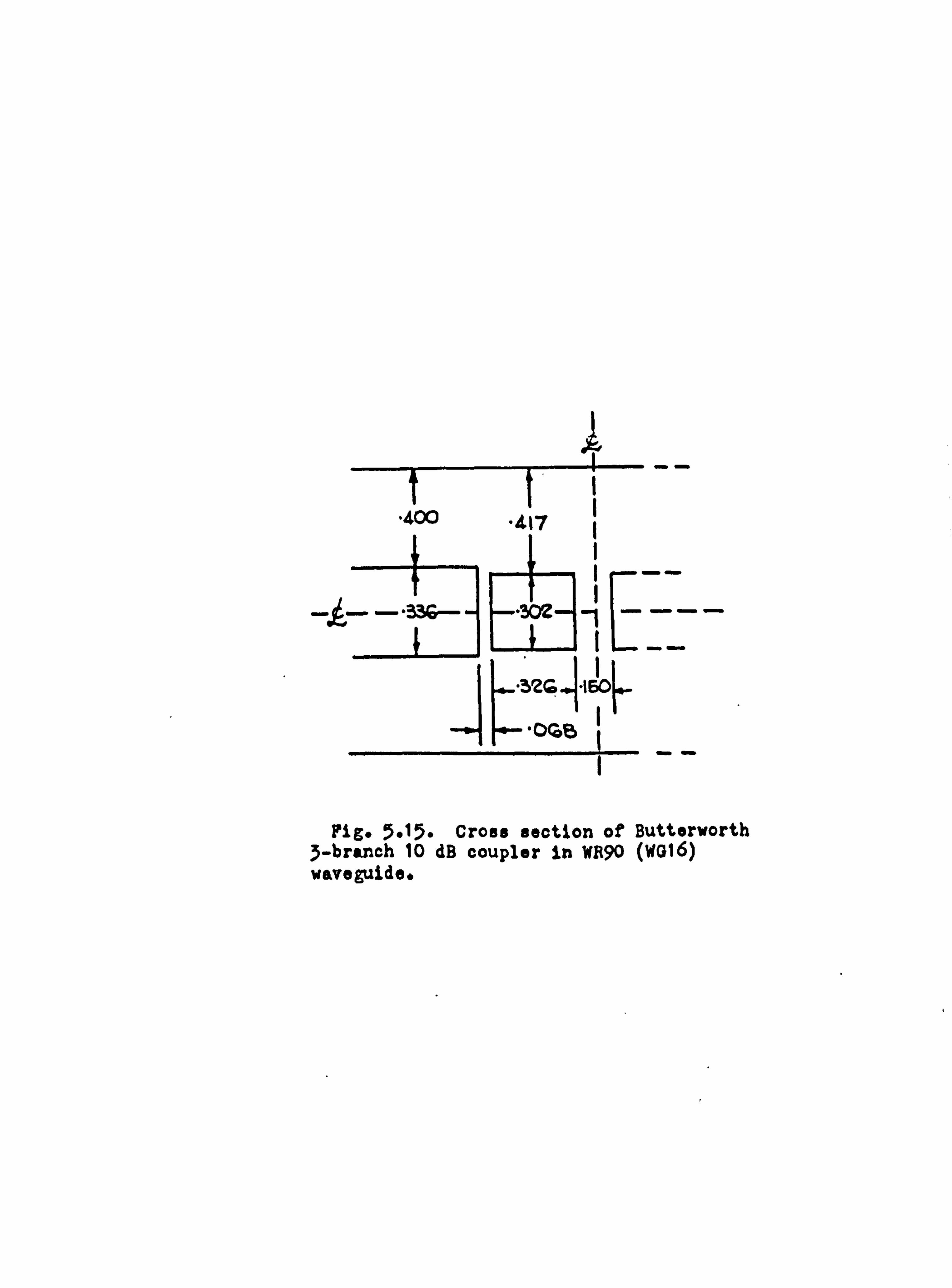
"400 . alb
--
-"ý-- "302 . -ý - -- -- F321*
"o6g
Fig. 505. Cross section of Butterworth 3-branch 10 dB coupler in WR90 (Wß16) waveguide.
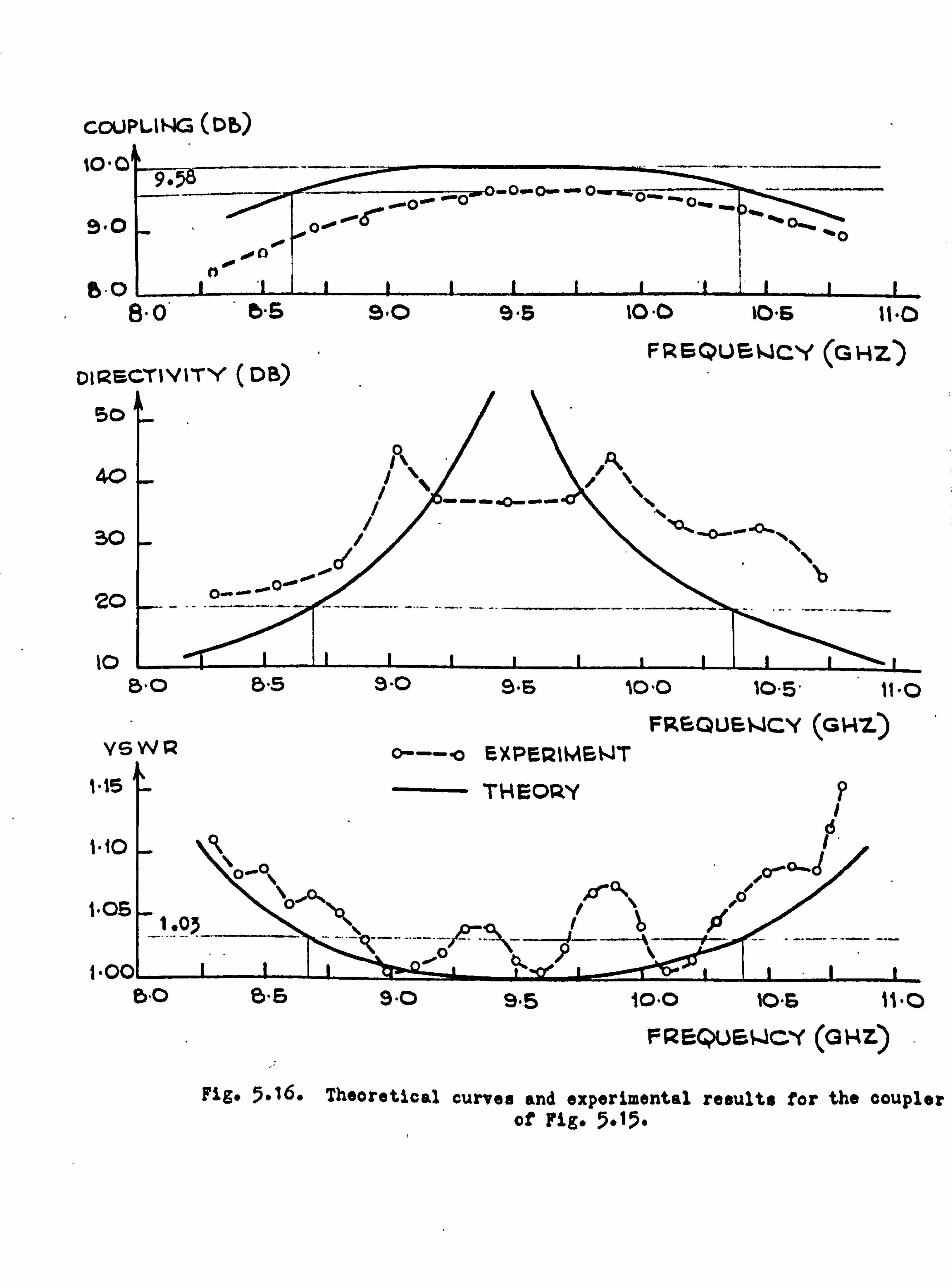
COUPLING (Db)
10.0 9--
6-: o-
6.0 o c"5 9.0
DIRECTIVITY (DB)
50
40
30 d
10
o'.. "bO
9 .5 10.0 10.6 11.0
FREQUSWCY (GHZ)
ß"0 5.5 5.0 9.6 10.0 10.5" 11.0
FREQUETJCY (GHZ)
Y5 WR o---. o EXPERIMENT
%'15 --- THEORY
6 1.10
odýo\ -o-a-d ö
ýý` 1.05 -
__ -- -, P" ------i' --ý -- -- - --- -- 1.00
5.0 15"5 9.0 9.5 io"O %0"& 11.0
FREQUEWCY (oNZ)
Fig. 5.16. Theoretical curves and experimental results for the coupler of Fig. 5.15"
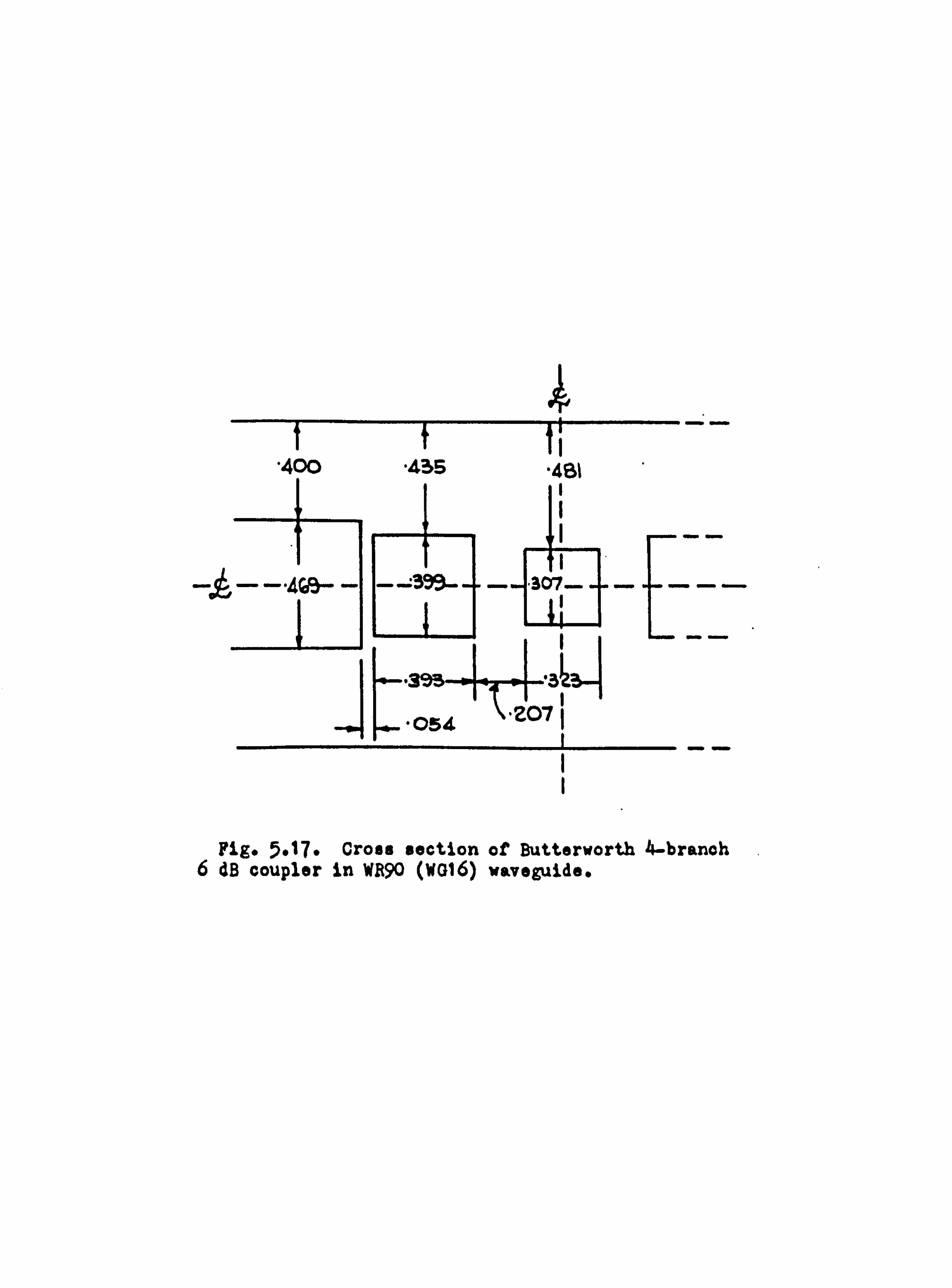
4
'400 "435 "4B
- --45- - H4+E-
"393 "32 I " 054
ý-'2071
I--
Fig. 5.17. Cross section of Butterworth 4-branch dB coupler in WR90 (WG16) waveguide.
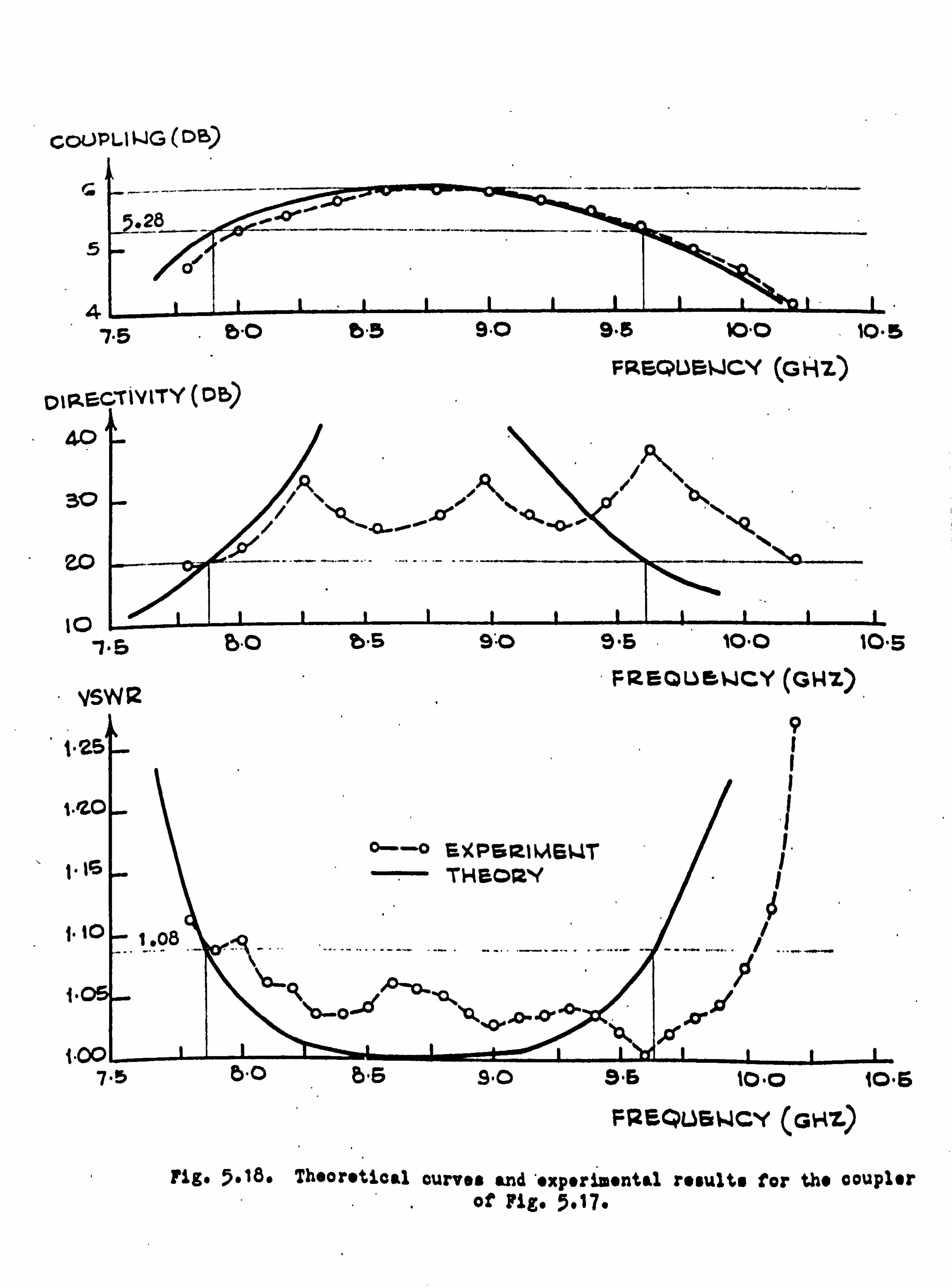
COUPLR-. G (DB)
: _TTT1'1
ý. 5 O fl3 9.0 9.5 10.0 10.3
FREQUEIJCY (G HZ)
01R1rcTIVITY (0b)
40 /A
310
10 7. cß 8O b"5 9.0 9.5 %0. O 10. S
VSWR FREOUMWCY (GNZ)
9 125 ý
vZO
Q---o EXPER% AEI"iT ý' 15 THEORY
1.1 O 1.08
1"
`Ib- q 100-0'1XI
1.00 7.5 ß 86 9. O 9.6 10.0 1O. 6
FREQl S 4cY ýGNZ)
Fig. 5.18. Theoretical curves end'sxpsrimsntsl results for the coupler of Fig. 5.17.

150
A 3-branch coupler constructed in stripline for a But-
terworth characteristic having 3 dB midband. coupling is
shown in Fig. 5.19. A photograph of this etripline coupler
(with the top ground plane removed) is shown in Fig. 5.20.
Reference (16) explains in detail the discontinuity corrections
that should be used in this design procedure. Originally de-
signed fora midband frequency of 1.5 GHZ, it actually centered
at 1.525 GHZ, -sad the theoretical cW-Puss ofFIg 5' drawn
oor. A9ngly, A similar coupler designed for Chebyehev perfor-
mance also gave excellent agreement between theory and experi-
ment for VBWR, ' directivity, and midband coupling, but showed
similar coupling deviations at the band edges. In these de-
eigne there is a large difference in width between the inner
and outer branch lines, and the length correction is different
from the two cases. However, a mean length correction is taken
in practice. This and other factors could be responsible for
deviations from strict theoretical performances at the band
edges.
An example of a broadband 5-branch waveguide coupler
designed for Chebyshev VSWR and directivity characteristics
is shown in Fige. 5.22 and 5.23. Here the midband coupling
is 8 dB, and for BW -L1.4 Table 5.2 gives a directivity ripple
of 24.2 dB, a. VBWR ripple level of 1.039, and a coupling which
drops to 5.74 dB at the band edges. The slightly nonequal
ripple performance is clearly indicated. The experimental
results agree quite closely with the theory..

"091 1
" 29ß
4--- 04. '1
ý4 " 478
ý.. _ 1.720 04-5009.
I 1.922
Fig. 5.19" Plan view of Butterworth 3-branch 3 dB'coupler in airspaced stripline, with ground-plane spacing 0.3125 inch and strip thickness 0.0625 inch.
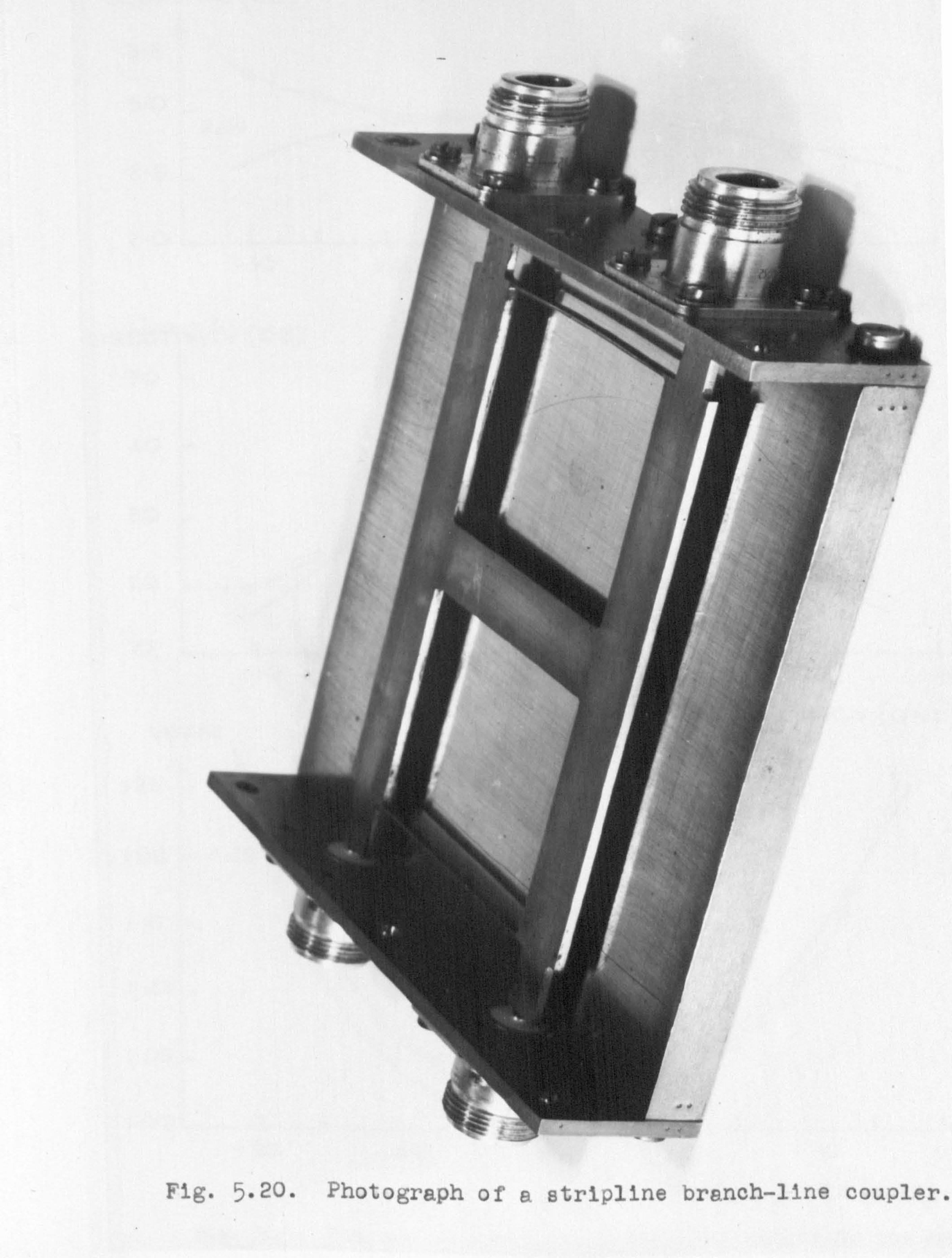
Fig. 5.20. Photograph of a stripline branch-line coupler.

COUPLIWO (05)
3.5
5.0 2.69
25
2. O 1.30
p1REG
50
4C
30
20
10
I No
1ý1ý1I 1\ 1
I. 4o 1 50 1.60 1.70 I. SO
FRSOUEWCY (GHZ)
1.30 I"ý40 i"50 I"ýo0 t"70 I. 80
VSWR FR sourav1CY (G Hz)
1.25
1.20 1.19 0-0 EX PER11r1EIJT -- -- ---- IT14E
1.15 i
ö\ d
I"lo ; °/
° 1.05 °1.1 fýý t . 525 ý Cýl
1.00 ýý1 II 1 113v 1.40 I"50 1-60 1.70 1"50
FRF-PUF- JC'C (GHZ)
Fig. 5.21. Theoretical curves and experimental results for the coupler of Fig. 5.19.

ý --
"400 "419 "446 ý
-"425- -"'ý7- - -"333- ----
"41 O "377-ý I+-
" 117
"040 Oi
Fig. 5.22. Cross section of Chebyehev 5-branch 8 dB coupler in WR90 (WG16) waveguide.

CýUPIýING (Dß)
ý g. 74
7.5 a'0 a'6
ýýREGTIVITYýDßý
50
24.2 20
lp 7,5 bO ib"5
vswR
t0
1. % t . 039b-«�>. , ý--o-_o-. ß-. °-
9.0 9.6 10.0 10.6 11.0
FREQL 4Y (GNZ)
%-. %ft
-- ---a -
5 .019.5 100 10.5 11.0
FREQUEIJCY (GHZ)
0--c B%PEP-IMEWT (x. THEORY
7,6 5"0 8.5 9O9.5 10.0 10.5 11. p
FREQUEIJCY (GHz)
Fig. 5.23" Theoretical curves and experimental results for the coupler of Fig. 5.22.

151
5.6 Concluding Remarks.
- One major restriction that was made in the approximation
part of the°, present design theory was that the functions
r'e/Te and r o/To
had as. many common zeros as possible. on.. the
imaginary axis of'the t-plane. This had the effect of giving
the... coupler perfect match and infinite directivity at these.
zero points.. As a result, the function F =(. e/Te - r"o/To was°
made'equiripple over the passband rather than (°e/Te itself.
To4see what would happen when f'e/Te was itself equiripple, the
following numerical experiment was performed. A three branch,
syrmetrical,, coupler with a bandwidth BW- 1.1 was used for both
prototypes. The Chebyshev design using equiripple F yielded
ýe/Te (1.00t5+ 2.05t3-ý- 1.00t)/(i-t2)2, having the values:
, -, ,.
Frequency point t n' /T ee
Lower band edge ,. 854 . 0209
Midband --- J1.00 -. 0250
Upper band edge , 1.17 . 0287
It is seen that Pe/Te is not equiripple over the bend. Next,
re/Te was made equiripple. For this case it was calculated
from an iteration process) that re /Tee w, (1.000t5#-2.075t34.
1.025t)/(l-t2)2. This function has zeros at t* "j. 9009 and
t= _* i 1.124. Now . 9009-1 - 1.110 and 1.12471-.. . 8898, and
therefore ('o/To will not have common zeros with re/Te 0 i. e.,

X52
this design will not have perfect match or perfect isolation
at any frequency. The comparison between the two designs is
summarized as follows:
Midband B. E. DIR VSWR Coupling Type COUP (Min) (Max) a1 a2 b1
20 dB old 19.88 36.82 1.001 . 0509 . 0993 1.0039
new 19.88 36.87 1.000 . 0508 . 0995 1.0047
10 dB cld 9.858 34.37 1.005 . 1656 . 3385 1.0451
new 9.859 34.40 1.004 . 1655 "3407 1.0486
3 dB old 2.826 30.41 1.045 "4330 1.3103 1.3899
new 2.829 30.35 1.046 "4332 1.3554 1.4138
In this chart the "old" type refers to the coupler designed
from+the F"function, whereas the "new" type refers to the case
where're/Te was made equiripple. It is seen that there is very
little difference between these two designs. Mathematically -.
speaking, however, much more work was done in adjusting roots
or coefficients until r e/TI was equiripple (as no closed form
solution is-known for this problem) than simply in using the
specification function Eq. (5.60)D which is given in closed
form. ! For ease of computation then, Eq. (5.60) was used in
designing Chebyshev couplers.
For both the Chebyshev and, Butterworth a uplere' the
coupling shows monotonic variation with frequency (with the
coupling becoming tighter away from center frequency), in
153
common with the previous theories. It was found that it was
possible to get some ripple in the coupling characteristic
with extreme input specifications, i. e., a directivity of
5-6 dB, BW- 1.4, and n- 3. For this same set of conditions
it was found that some of the branch lines were calculated to
have negative values. All reasonable input specifications
(such as appear in the Tables) resulted in the coupling vs.
frequency curve having a parabolic shape. In general it was
observed that to have the coupling as flat as possible over
the band it was necessary to use a Chebyshev design with as
large a bandwidth as possible. Recall from the design curves
(Figs-5.8 to 5.11) that as bandwidth becomes larger so does the
ripple VSWR, with the minimum directivity falling in value.
To achieve as flat a coupling as possible therefore, the band-
width should be increased until either the VSWR or directivity
reaches the allowable design specification limit.
In many synthesis techniques there is no control over the
resulting element values; such is the case also with the new
coupler design theory. In fact with this theory there is no
assurance that the branch-line element values will even turn
out to be positive, due to the structural realization deman-
ded. A numerical experiment was performed to see if, by chang-
ing the structure slightly, a lower element value ratio could
be achieved. It was decided to relax the double-length re-
154
quirement for the main line unit elements, and allow them to
become two'single-length unit elements of different impedances.
A maximally flat three branch symmetrical design was used. It
was arranged that=the first branch line stub-. was increased in
value, while keeping the even mode C/T characteristic maximally
flat (two zeros at midband). This did result in the main line
unit elements becoming stepped, and it also resulted in a lower
element-value ratio. -Upon analyzing the odd mode r/T, however,
it was found that the quartet of zeros of Po were now at
t s ±"447 ril. 169-instead of at ±jl(double zeros). The VSWR
and isolation performance of this design around midband was
clearly inferior to the original maximally flat design because
of the relatively large value of ('o at these frequencies. Thus,
the element value ratio cannot be improved in this manner with-
out degrading design performance.
It may be shown that waveguide realizations of Tables
5.1 and 5.2 can only be made for couplings looser than 5 or 6
dB. This is because, for tighter couplers, the branch guides
become very large in size with the result that the metal
separating two adjacent branch guides becomes a narrow post.
Then there is no longer a branch-guide coupler but a wave-
guide structure which will have a complicated field pattern.
Similarly, stripline couplers with a looser coupling than'5 or
6, dB-are unrealizable because of the range of element values.
In previous designs of waveguide branch-guide couplers, it was
155
possible-to arrive at 3 dB designs. With the new theory,
however., the only way to arrive at a3 dB waveguide coupler is
, to cascade two: 8.34 dB coupler designs together. With this
technique, more branches may be necessary than would be re-
quired in"using an-older design technique! It is-obvious then
that for some input specifications there will be a 00tradeoffl
between optimum performance and realizability.. An important
unsolved problem in branch-guide coupler design is to find a
method of degrading the'frequency performance in such a way as
to lower the element value ratio until a waveguide (or strip-
line) design is realizable. In this context the performance
data of couplers described herein may be used as a standard
in order to measure the degradation suffered in achieving
realizability.
The new synthesis technique for branch-guide directional
couplers, in the many cases where a structure is directly
realizable, gives superior results compared with previous ap-
proximate methods for Butterworth and Chebyshev VSWR and
directivity characteristics. The results for practical
branch-guide couplers designed using the new theory give
good agreement with the computed results, and the design of
couplers having a bandwidth greater than one octave appears
to be feasible. The design procedure is simplified by the
publication of tables of branch guide and main line immit-

156
tance values for both the symmetric and asymmetric case, which
cover most specifications of practical interest. The asym-
metric case represents a new structure, which, by combining
the properties of a coupler and impedance transformer, will
result in a much more economical structure in certain applica-
tions.
Branch-guide couplers in stripline are widely used in
microwave miniature circuits, and the broadband designs given
here could be utilized for such applications.

157
Chapter 5 REFERENCES
1. Young, L.: "Advances in Microwaves, Vol. 1Q. Academic
Press, 1966, pp. 118-126.
2. Van Valkenburg, M. E.: "Introduction to Modern Network
Synthesis". Wiley, 1960, pp. 424-430- 3- Young, L.: "Synchronous branch-guide directional couplers
for low and high power applications", IRE Trans. MTT,
Vol. 10, Nov. 1962, pp. 459-475.
4. Young, L.: "Advances in Microwaves, Vol. 10. Academic
Press, 1966, pp. 155-161.
5. Lower, P. D. and Crompton, J. W.: "A new form of hybrid
junction for microwave frequencies. " Proc. Inst.
Elec. Engrs. (London), Vol. B104,1957, pp. 261-264-
6. Levy R.: "A guide to the practical application of
Chebyshev functions to the design of microwave
components. Proc. Inst. Elec. Engrs. (London),
Vol. C106D 19599 PP. 193-199"
7. Patterson, K. G.: "A method for accurate design of a
broadband multibranch waveguide coupler. " IRE,
Trans. MTT, Vol. 7, Oct. 19599 PP- 466-473" 8. Levy, R.: "Tables of element values for the distributed
low-pass prototype filter. " IEEE, Trans. MTT,
Vol. 13,1965, PP. 514-536.
158
9. Levy, R. and Lind, L. F.: "Synthesis of symmetrical branch-
guide directional couplers, " IEEE, Trans. MTT, Vol. 16,
Feb. 1968, pp. 80-89.
10. Lind, L. F.: "Synthesis of asymmetrical branch-guide direc-
tional coupler-impedance transformers. " (Accepted for
publication in IEEE Trans. Microwave Theory and Tech-
niques).
11. Riblet, H. J.: "The application of a new class of equal-
ripple functions to some familiar transmission-line
problems, " IEEE Trans. MTT, Vol. MTT-12, July, 1964,
PP- 415-421.
12. Carlin, H. J. and Kohler, W.: "Direct synthesis of band-pass
transmission line structures, " IEEE Trans. MTT, Vol.
MTT-13, may, 1965, pp. 283-297.
13. Tuttle, D. -F.: "Network Synthesis, Vol. 1. " Wiley, 1958,
Appendix B.
14. Kurokawa, K.: "Design theory of balanced transistor
amplifiers, " Bell System Technical Journal, Vol. 44,
No. 8, October, 1965, pp. 1675-1698.
15. Matthaei, Young, and Jones: "Microwave Filters, Impedance-
Matching Networks, and Coupling Structures. " McGraw-
Hill, 1964, pp. 835-840.
16. Matthaei, Young, and Jones: "Microwave Filters, Impedance-
Matching Networks, and Coupling Structures. " Mcaraw-
Hill, 1964, pp. 208-211.

159
Chapter 6
Conclusions and Possible Developments
In this thesis the following two problems have been
investigated
(1) Synthesis of equally terminated, lumped and distribu-
ted filters containing an even number of elements.
(2) Synthesis of symmetrical and asymmetrical branch-
guide directional couplers.
The solution of (1) was found to be straightforward once
the insertion loss has been specified. The. standard Darlington
synthesis technique is employed, which leads to a unique solu-
tion (since all of the insertion loss zeros are on the frequency
axis). It appears likely, however, that there may exist closed
formulae for the element values which are direct functions of
the inputispecifications (number of sections and Passband ripple
level) for the lumped filters. Formulae of this sort have
already been determined for lumped filters having a "pure"
Chebyshev insertion loss description. The new formulae, if they
exist, would simplify design since the Darlington synthesis
procedure could then be eliminated. Discovery of these formu-
lae would be a very useful and practical project.
The solution of (2) has also been accomplished for the
case where the directivity and VSWR of the coupler are speci-
fled. It is found that this new technique gives superior
results compared with previous approximate. methods both for
16o
`Butterworth and Chebyshev specifications. ` The coupling shows
monotonic variation with frequency; in common with previous
theories. The coupling variation is an output of, the-design
procedure, rather than an input. Computer results show that
when the coupling is made very flat or with ripple over the,
passband the coupler will have poor directivity and high-VSWR.
An attempt could be-made, however, to arrive at a-specification
function for, the coupler which contains coupling information as
well as VSWR and directivity information. Then the "tradeoff"
between these three parameters would be brought to light.
Another difficulty with the new design procedure is that
one has no control over the element values which will appear
at the output of the procedure. In fact it has already been
seen that due to the structural form demanded, negative. element
values might occur. In practice it has been found however
that reasonable input specifications result in reasonable
element values. Tables have been prepared for a large variety
of input specifications. A scan of these tables will quickly
reveal which realizations are possible for a given type of transmission line network. An important problem arises here.
Assume that certain input specifications for the coupler must be met, and a table scan shows that all such designs meeting
or exceeding these specifications are unrealizable. Then
the (optimum) design specification function must be degraded

161
in such a manner as to arrive at realizable element values.
The degradation itself should be as small as possible. This
problem has not been solved yet, and it is felt that an analy-
tical solution to this problem would be very difficult to find.
From a practical viewpoint, however, this problem is very im-
portant. A possible numerical solution to this problem might
be obtained from a trial and error procedure contained in a
computer program.