jucetize.weebly.com · service / training manual lcd digital color tv az3fk cassis s: p-2f...
TRANSCRIPT

SERVICE / TRAINING MANUAL
LCD Digital Color TV
AZ3FK ChassisSegment: P-2F
9-883-873-05
Self DiagnosisSupported model
Version Date Subject1.0 2/24/2012 Original Manual Release Date.2.0 3/5/2012 Insulation Sheets added to Disassembly Section. Replaced page 18.3.0 3/8/2012 P/N’s for Vesa Bracket removed from Disassembly Section. Replaced page 15.4.0 7/27/2012 New caution added on page ii. Updated Service Adjustments section. Replaced pages 24 - 27. 5.0 8/14/2012 Updated P/N’s list from Disassembly Section. Replaced pages 17 - 20.
ORIGINAL MANUAL ISSUE DATE: 3/2012
HISTORY INFORMATION FOR THE FOLLOWING MANUAL:

SERVICE / TRAINING MANUAL
LCD Digital Color TV
AZ3FK ChassisSegment: P-2F
9-883-873-05
Self DiagnosisSupported model
KDL-40BX450

MODEL LIST MODEL COMMANDER DESTINATION MODEL COMMANDER DESTINATION
9-883-873-05
KDL-40BX450 RM-YD080 US/CND
KDL-40BX450 RM-YD080 LA/MX
KDL-40BX451 RM-YD080 CND
KDL-40BX451 RM-YD080 MX
KDL-46BX450 RM-YD080 US/CND
KDL-46BX450 RM-YD080 LA/MX
KDL-46BX451 RM-YD080 MX

KDL-40BX450/40BX451/46BX450/46BX451 i
TABLE OF CONTENTS
Cautions and Warnings ...................................................................................iiSection 1 - Features and Overview ................................................................1
Features ........................................................................................................1Specifications ................................................................................................1Chassis Overview ..........................................................................................3Overall Circuit Description .............................................................................4
Main Board ...............................................................................................4Power Supply Board .................................................................................4IR Board ....................................................................................................4Switch Unit ................................................................................................4LCD Panel Assembly ................................................................................5
Section 2 - Troubleshooting ...........................................................................6Overview .......................................................................................................6
Updating the Software ..............................................................................6Self Diagnosis Function .................................................................................6
Standby LED Blink Count .........................................................................6Viewing the Self Check Diagnosis History ................................................7
Triage Chart ...................................................................................................8Section 3 - Flow Charts and Diagrams ..........................................................9
Block Diagram ...............................................................................................9No Power .....................................................................................................10Standby LED Blinking ..................................................................................12No Video ......................................................................................................13
Section 4 - Disassembly/Part Number Information ....................................15Table-Top Stand and Rear Cover Removal .................................................15Main Board (A) and Power Supply Board (G10/G11) Removal ...................16Panel Brackets and LCD Panel Removal ....................................................17
Cleaning the LCD Panel .........................................................................17
Connectors ..................................................................................................18Screws ........................................................................................................18Accessories and Packaging ........................................................................19Miscellaneous ..............................................................................................19Remote Commander ...................................................................................19Wire Dressing ..............................................................................................20
Section 5 - Updates and Adjustments .........................................................21Overview .....................................................................................................21Software Updates for Customers ................................................................21Software Updates for Servicers ...................................................................21
Software Update Responsibility ..............................................................22Checking the Software Version ...............................................................22Examples of Software Correctable Symptoms .......................................22
Accessing Service Adjustment Mode ..........................................................23Completing Service Requirements When Replacing the Main Board .........24
Viewing the Status Information ...............................................................24Selecting the Panel ID Code ...................................................................25Adding the Serial Number .......................................................................26Adding the Model Name .........................................................................27
Completing Service Requirements When Replacing the LCD Panel ..........29Verifying the Panel ID Code ....................................................................29Resetting Panel Operation Time .............................................................30
Accessing Factory Adjustment Mode ..........................................................31Adjusting the Color Temperature ............................................................31
Appendix A: Encryption Key Components ............................................... A-1

KDL-40BX450/40BX451/46BX450/46BX451 ii
CAUTION!!These servicing instructions are for use by qualified service personnel only. To reduce the risk of electric shock, do not perform any servicing other than that contained in the operating instructions unless you are qualified to do so.
WARNING!!An isolation transformer should be used during any service to avoid possible shock hazard, in case of live chassis.
! SAFETY-RELATED COMPONENT WARNING!!There are critical components used in LCD color TVs that are important for safety. These components are identified with shading and ! mark on the schematic diagrams and the parts list. It is essential that these critical parts be replaced only with the part number specified in the parts list to prevent electric shock, fire or other hazard.
NOTE: Do not modify the original design without obtaining written permission from the manufacturer or you will void the original parts and labor warranty.
ATTENTION!!For safety reasons, component level repair of the Power Supply Boards and/or the Inverter Boards is prohibited.
CAUTIONS AND WARNINGS
ATTENTION!!Ces instructions de service sont à l’usage du personnel de service qualifié seulement. Pour prévenir le risque de choc électrique, ne pas faire l’entretien autre que celui contenu dans le Mode d’emploi à moins que vous soyez qualifié faire ainsi.
ALERTE!!Afin d’eviter tout risque d’electrocution provenant d’un chássis sous tension, un transformateur d’isolement doit etre utilisé lors de tout dépannage.
! ATTENTION AUX COMPOSANTS RELATIFS A LA SECURITE!!
Les composants identifies par une trame et par une marque ! sur les schemas de principe, les vues explosees et les listes de pieces sont d’une importance critique pour la securite du fonctionnement. Ne les remplacer que par des composants Sony dont le numero de piece est indique dans le present manuel ou dans des supplements publies par Sony. Les reglages de circuit dont l’importance est critique pour la securite du fonctionnement sont identifies dans le present manuel. Suivre ces procedures lors de chaque remplacement de composants critiques, ou lorsqu’un mauvais fonctionnement suspecte.
ATTENTION!!Pour des raisons de sécurité, Interdire de réparer ou remplacer les composantes dans les blocs d’alimentation et/ou sur les modules d’inverseur.
KDL-40BX450/40BX451/46BX450/46BX451 iii
CAUTIONS AND WARNINGS
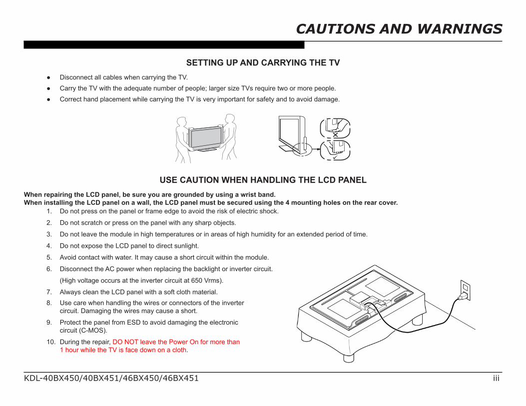
SETTING UP AND CARRYING THE TV Disconnect all cables when carrying the TV. Carry the TV with the adequate number of people; larger size TVs require two or more people. Correct hand placement while carrying the TV is very important for safety and to avoid damage.
USE CAUTION WHEN HANDLING THE LCD PANELWhen repairing the LCD panel, be sure you are grounded by using a wrist band.When installing the LCD panel on a wall, the LCD panel must be secured using the 4 mounting holes on the rear cover.
1. Do not press on the panel or frame edge to avoid the risk of electric shock.
2. Do not scratch or press on the panel with any sharp objects.
3. Do not leave the module in high temperatures or in areas of high humidity for an extended period of time.
4. Do not expose the LCD panel to direct sunlight.
5. Avoid contact with water. It may cause a short circuit within the module.
6. Disconnect the AC power when replacing the backlight or inverter circuit.
(High voltage occurs at the inverter circuit at 650 Vrms).
7. Always clean the LCD panel with a soft cloth material.8. Use care when handling the wires or connectors of the inverter
circuit. Damaging the wires may cause a short.
9. Protect the panel from ESD to avoid damaging the electronic circuit (C-MOS).
10. During the repair, DO NOT leave the Power On for more than 1 hour while the TV is face down on a cloth.

KDL-40BX450/40BX451/46BX450/46BX451 iv
CAUTIONS AND WARNINGS
CLEANING THE LCD PANELCAUTION: When cleaning the TV, be sure to unplug the power cord to avoid any chance of electric shock.
Clean the cabinet of the TV with a dry soft cloth.Wipe the LCD screen gently with a soft cloth.
; Stubborn stains may be removed with a cloth slightly moistened with a solution of mild soap and warm water. ; If using a chemically pretreated cloth, please follow the instruction provided on the package. ; Never use strong solvents such as a thinner, alcohol or benzine for cleaning. ; Periodic vacuuming of the ventilation openings is recommended to ensure proper ventilation.
; Do Not use paper towels, any type of abrasive pad, rags, rubber or vinyl materials to clean the screen. Using these materials could easily scratch the screen which may result in permanent damage.
; Do Not use any cleaning product containing alkaline/acid cleaner, scouring powder or volatile solvent, such as alcohol, ammonia, benzine, thinner or insecticide. Using any of these harsh cleaners may result in permanent damage to the screen.
; Do Not spray water or detergent directly onto the TV screen. If liquid drips into the bottom of the screen it may cause a failure.

KDL-40BX450/40BX451/46BX450/46BX451 v
CAUTIONS AND WARNINGS
SAFETY CHECK-OUTAfter correcting the original service problem, perform the following safety checks before releasing the set to the customer:
1. Check the area of your repair for unsoldered or poorly soldered connections. Check the entire board surface for solder splashes and bridges.
2. Check the interboard wiring to ensure that no wires are “pinched” or touching high-wattage resistors.
3. Check that all control knobs, shields, covers, ground straps and mounting hardware have been replaced. Be absolutely certain that you have replaced all the insulators.
4. Look for unauthorized replacement parts, particularly transistors, that were installed during a previous repair. Point them out to the customer and recommend their replacement.
5. Look for parts which, though functioning, show obvious signs of deterioration. Point them out to the customer and recommend their replacement.
6. Check the line cords for cracks and abrasion. Recommend the replacement of any such line cord to the customer.
7. Check the antenna terminals, metal trim, “metallized” knobs, screws and all other exposed metal parts for AC leakage. Check leakage as described in “Leakage Test”.
LEAKAGE TESTThe AC leakage from any exposed metal part to earth ground and from all exposed metal parts to any exposed metal part having a return to chassis, must not exceed 0.5 mA (500 microamperes). Leakage current can be measured by any one of three methods.
1. A commercial leakage tester. Follow the manufacturers’ instructions provided with the tester.
2. A battery-operated AC milliammeter.
3. Measuring the voltage drop across a resistor by means of a VOM or battery-operated AC voltmeter. The “limit” indication is 0.75 V, so analog meters must have an accurate low voltage scale. Nearly all battery-operated digital multimeters that have a 2 VAC range are suitable. (see Figure A)
To Exposed MetalParts on Set
0.15 µF
Earth Ground
ACVoltmeter(0.75V)
Figure A. Use an AC voltmeter to check AC leakage.
HOW TO FIND A GOOD EARTH GROUNDThe cover-plate retaining screw on most AC outlet boxes is at earth ground. Verify the AC outlet box retaining screw ground by connecting a 60W to 100W incandescent (not a neon or fluorescent lamp) between the hot side of the receptacle and the retaining screw. Try both slots, if necessary, to locate the hot side on the line; the lamp should light at normal brilliance if the screw is at ground potential. (see Figure B)
Figure B. Checking for earth ground.
Trouble Light
AC Outlet Box

KDL-40BX450/40BX451/46BX450/46BX451 1
FEATURESThe AZ3FK chassis is one of several designs for the 2012 model line of Sony Bravia® LCD televisions. This manual covers the following models: KDL-40BX450 KDL-40BX451 KDL-46BX450 KDL-46BX451
The BRAVIA® Sync™ BX45x series LED LCD HDTV Brilliant Full HD (1080p) picture quality Four HD inputs for a cable box, PS3™ and more1 Share your pictures on the big screen via USB input Crisp detail & contrast w/ Clear Resolution Enhancer Optimized picture based on what you’re watching Less grain & a clear picture w/ Digital Noise Reduction Theater-like movie viewing with 24p True Cinema One remote for multiple devices with BRAVIA® Sync™2
SECTION 1 - FEATURES AND OVERVIEW
SPECIFICATIONSSystemTelevision system
ATSC (8VSB terrestrial): ATSC compliant 8VSBQAM on cable: ANSI/SCTE 07 2000 (Does not include CableCARD functionality)
Channel coverageAnalog Cable: 1 - 135 / Digital Cable: 1 - 135
Panel system
Speaker outputKDL-46/40BX451: 8 W + 8 W
Input/Output jacksCABLE/ANTENNA
VIDEO IN 1AUDIO: 500 mVrms (Typical) / Impedance: 47 kilohms
COMPONENT IN YPBPR (Component Video): Y: 1.0 Vp-p, 75 ohms unbalanced, sync negative / PB:0.7 Vp-p, 75 ohms
PR : 0.7 Vp-p, 75 ohms / Signal format: 480i, 480p, 720p, 1080i, 1080pAUDIO: 500 mVrms (Typical) / Impedance: 47 kilohms
HDMI IN 1/2Audio: Two channel linear PCM 32, 44.1 and 48 kHz, 16, 20 and 24bits, Dolby Digital
PC Input (see Operating Instructions)
AUDIO OUT
DIGITAL AUDIO OUT (OPTICAL)
PCM/Dolby Digital optical signal
evitisop ,smho 57 ,p-pV 7.0 ,BGR golana ,nip-51 bus-DNI CPSee the PC Input Signal Reference Chart for PC and HDMI IN
PC/HDMI IN 1 AUDIO IN
oediV dna cisuM ,otohP :054XB04/64-LDKBSUKDL-46/40BX451: Photo and Video
NTSC: American TV standard
Analog terrestrial: 2 - 69 / Digital terrestrial: 2 - 69
LCD (Liquid Crystal Display) Panel
KDL-46/40BX450: 6 W + 6 W
75-ohm external terminal for RF inputs
VIDEO: 1 Vp-p, 75 ohms unbalanced, sync negative
HDMI: Video: 480i, 480p, 720p, 1080i, 1080p, 1080/24p
500 mVrms (typical)
Stereo mini jack, 500 mVrms, (Typical) / Impedance: 47 kilohms
1. Cables sold separately.
2. Syncs with BRAVIA® Sync or Theatre Sync™ products.

KDL-40BX450/40BX451/46BX450/46BX451 2
SECTION 1 - FEATURES AND OVERVIEW
• Optional accessories availability depends on its stock.• Design and specications are subject to change without notice.* Dimensions and mass are approximate values.
Mass*(lb)
17.237.9
13.830.4
without stand (kg)(lb)
16.035.3
12.828.2
Supplied accessoriesGuide (1)/Warranty Card (1)/Safety and Regulatory Booklet (1)/Software License (1)/Stand
installation guide (1)/Table-Top Stand (1 set)/Screw (3)common to all models
Optional accessories
Remote Control RM-YD080 (1)/Size AA batteries (2)/Operating Instructions (1)/Quick Setup
Connecting cables / Support Belt Kit / Wall-Mount Bracket: SU-WL500
(mm)
with stand (kg)
Model name KDL-46BX450KDL-46BX451
KDL-40BX450KDL-40BX451
Power and othersPower requirement
Power consumptionW 851W 881
in use
in standby
Screen size*(inches measured diagonally) 0464
)lacitrev( senil 080,1 × )latnoziroh( stod 029,1 noituloser yalpsiD
Speaker/Full range (2)(inches)
40 × 100(1 5/8 × 4)
Dimensions* with stand(inches)
1,112 × 713 × 27943 7/8 × 28 1/8 × 11
980 × 639 × 23138 5/8 × 25 1/4 × 9 1/8
without stand (mm)(inches)
1,112 × 675 × 9743 7/8 × 26 5/8 × 3 7/8
980 × 601 × 9438 5/8 × 23 3/4 × 3 3/4
wall-mount hole pattern (mm) 300 × 300
wall-mount screw size (mm) M6 (length: 8-12mm)
Less than 0.2 W with 120 V AC and with 240 V AC less than 0.3 W
110-240 V AC, 50/60 Hz (U.S.A./Canada/Mexico 120 V AC, 60 Hz)
(mm)

KDL-40BX450/40BX451/46BX450/46BX451 3
SECTION 1 - FEATURES AND OVERVIEW
CHASSIS OVERVIEWThe primary circuits in the AZ3FK chassis consist of a Main Board (A Board), Power Supply Board (G10 Board for the 40” models and G11 Board for the 46” models), the IR Board (H Board), the Switch Unit and the LCD Panel Assembly which includes the TCON Board and the Inverter MT Board.NOTE: For connector part number information, refer to “Connectors” on page 18. For Wire Dressing information, refer to “Wire Dressing” on page 20.
SWITCHUNIT
INV
A
H
G10/G11
BOARD LAYOUT EXAMPLE FOR ALL MODELS

KDL-40BX450/40BX451/46BX450/46BX451 4
SECTION 1 - FEATURES AND OVERVIEW
CPU: The CPU internal to the MT5389 processor controls all aspects of the television functions. Input from the user along with monitoring of critical circuits is also performed by this CPU.LVDS Transmitter: Integrated into the MT5389 is a Low Voltage Differential Signaling (LVDS) transmitter. This circuit converts the 8-bit parallel RGB video information into a set of high speed serial lines for noise-free transmission to the TCON circuits located internally to the LCD panel.
POWER SUPPLY BOARDThere are 2 different Power Supply boards used in the models in this manual. The type of board depends on the size of LCD panel. They are:
G10 for the 40” models G11 for the 46” models
There are 2 distinct sections on the power supply:Standby Supply: Continuously operational as long as AC power is applied, the standby supply generates 3.3VDC for the circuits requiring power while the unit is turned off. An unregulated 15-volt line is present to provide power to the main relay, PFC and main power supply at turn-on.Main Supply: Once the power supply receives a power-on command from the CPU on the A board, the main switching supply is turned on to provide a regulated 12V source, a dedicated un-regulated 15V for the audio circuits and an unregulated 24V source for the inverter circuit.
IR BOARDDesignated as the H Board, the IR Board contains the power, standby and timer LED’s that is located on this board along with the IR remote receiver and light level sensor.
SWITCH UNITThis board contains the power, channel and volume up/down and menu buttons.
OVERALL CIRCUIT DESCRIPTIONThe “Block Diagram” on page 9 provides an overview of the AZ3FK chassis. The following are descriptions of the boards and their functions.
MAIN BOARDCommon to all models utilizing the AZ3FK chassis, the Main Board (A Board) contains most of the video processing circuitry along with all audio processing. Control of the television is accomplished via a CPU embedded within the MT5389 processor. Below is a list of the key components located on the Main Board.
TUNERThe tuner is a combination ATSC/NTSC unit. It can receive traditional analog NTSC signals via cable or terrestrial along with ATSC digital signals via terrestrial (8VSB) or cable (64 or 256 QAM).
MT5389PROCESSORThis IC performs the majority of the necessary audio and video processing on the Main Board.Analog Video Input Switch: All analog video sources are selected and A/D converted and scaled (if necessary) to 1920 X 1080p 60HZ resolution.Digital Audio and Video Decoder: The MPEG2 and Digital Dolby audio streams are received from the tuner for decompression. All video sources which are not native 1920 X 1080p 60HZ are scaled to this resolution. Digital audio content is output to the class D amplifier for processing and amplification.Audio Processing: Analog audio sources are selected and A/D converted directly by the MT5389. The audio information is then processed digitally. Digital audio from the tuner and HDMI sources is also input and processed. Class D amplifier provides the drive for the speakers.HDMI Input and Switching: The customer can select the HDMI1 through HDMI2 input. Each HDMI input contains a dedicated EDI NVM (not shown) to provide display information data to any device connected via the HDMI inputs.

KDL-40BX450/40BX451/46BX450/46BX451 5
SECTION 1 - FEATURES AND OVERVIEW
LCD PANEL ASSEMBLYThe LCD Panel Assembly includes the LCD Panel, TCON Board and Backlight system.The LCD Panel contains the actual liquid crystals, color filters and polarizers. The liquid crystals are manipulated by the applied voltage to pass a specific amount of light - from the backlight - depending on the level of voltage applied.The TCON performs all the control, timing, charge and discharge functions driving the operation of the LCD Panel.A new LCD Panel Assembly from parts will include the following items:
LCD Panel TCON Board Inverter MT Board
TCON BOARDThe TCON Board communicates between the LCD Panel and the microprocessor on the Main Board. NOTE: The TCON Board is not available as a replacement part for all models. To determine if the TCON Board is available as a replacement part, refer to the LCD Panels Manual.
INVERTER MT BOARDThe inverter receives the unregulated 24V from the Power Supply Board and generates the required high voltage AC to power the backlight lamps. A control line to turn on the inverter (backlights on) is used in conjunction with a dimmer control to vary the light level of the CCFL lamps.

KDL-40BX450/40BX451/46BX450/46BX451 6
OVERVIEWThis chapter provides information regarding the Self Diagnosis feature in our TVs.
UPDATING THE SOFTWAREThe Self Diagnosis function is designed to provide information regarding the problem with the TV, however, there are several issues that may be resolved by updating the TV software to the latest version. Always check the Sony Authorized Servicer Portal at http://www.sony.com/asp for any issues that are software related. Most symptoms that are correctable by software updates involve communications issues with other devices or minor glitches in the operation of a specific function. Below is a list of some of the symptoms that may be corrected with a software update:
Fluctuations in picture brightness Intermittent picture freezing or noise Problems with certain inputs (especially HDMI) Intermittent or distorted audio Erratic remote control operation TV turns on and off by itself Loss of color Internet connectivity Certain features not working correctly
(photo or video file viewing)
SECTION 2 - TROUBLESHOOTING Self DiagnosisSupported model
SELF DIAGNOSIS FUNCTIONCritical voltages and circuit operations are monitored by the CPU on the Main Board. If an error is detected the Self Diagnosis function in the TV will force the TV to shut down by the CPU. The monitored circuit in which the fault occurred will automatically cause the CPU to blink the Standby LED in groups of repeating sequences. The number of times the Standby LED blinks indicates the possible cause of the problem. Not all of the available protect codes are used in every model. For example, models that don’t have the local dimming feature do not use the 4X blink error as this circuit is found in models that are backlit with fluorescent lamps. The information in this section provides guidance in locating the possible component causing the shutdown.
STANDBY LED BLINK COUNT
Standby LED
2 times
5 times
LED ON 0.3 sec.
LED OFF 0.3 sec. LED OFF3 sec.
LED DISPLAY & BLINK COUNT

KDL-40BX450/40BX451/46BX450/46BX451 7
SECTION 2 - TROUBLESHOOTING
VIEWING THE SELF CHECK DIAGNOSIS HISTORYWhen an error is detected, the Self Check screen records the number of times the error occurred. This is helpful in confirming past occurrences of an error and for determining if an error is intermittent when the customer is not sure what is causing the television to shut down. If the screen displays a “0”, no error has occurred.
1. TV must be in Standby mode.2. Press the following buttons on the Remote Commander within a
second of each other:
DISPLAY Channel 5 Volume + POWER
3. To access the Self diagnosis history page, press until Self diagnosis history is highlighted.
Sound Adjustment >>Wide Band Tuning >>Range Scan… >>Self diagnosis history >>Status Information… >>LVDS Spectrum(%0) <[ 20 ]>DPMS <[ Off ]>Low of HPD <[ 5 ]>TVD_MCDONE_CNT <[ 20 ]>Demo Special >>Bypass AVI Info Detect <[ On ]>Panel Selection <[ 13_FHD_SLCD_40 ]>UART Selection No LogSERIAL NUMBER EDITMODEL NAME EDIT
[</>]Set [Home] Exit
Service Mode
4. Then press to view the Self Check screen.
Back <<002 MAIN_ POWER 001003 AUDIO_PROT 000003 DC_ALERT1 000004 BALANCER 000005 TCON_ERR 000005 PANEL_POWE 000006 BACKLITE 000007 TEMP_ERR 000
00150 00075 00007
[Menu] Exit
SELF CHECK
Indicates no error has occurred
Indicates an error has occurred
SAMPLE SELF CHECK DIAGNOSIS PAGE
2X Blink - Main Power ErrorA loss of REG12V from the power supply triggers this protect event. The usual cause is a failure of the main switching supply. In some instances, excessive loading on the secondary supply lines can cause the switching regulator to stop or fail again, if a replacement board is installed.
3X Blink- DC Regulator/Audio ErrorThe REG 5V and D3.3V source originating on the Main Board is monitored for low-voltage conditions by the CPU. A failure causing a 3X shutdown requires replacing the Main Board.
4X Blink – Balancer ErrorNOT USED IN THIS MODEL SERIES.
5X Blink - TCON Error/Panel ErrorThe 5X blink protection mode indicates a communications error with the timing control circuits (TCON Board) has occurred. If the TCON Board is available for replacement, replace it, if not, replace the LCD Panel Assembly. In rare cases a loose or defective LVDS cable could also be the cause.

KDL-40BX450/40BX451/46BX450/46BX451 8
SECTION 2 - TROUBLESHOOTING
6X Blink - Backlight Inverter System FailureIf the inverter circuits fails to generate high voltage or one or more of the backlight lamps fails to light, the television will shut down and display this diagnostics error. Observing for the presence of backlighting is crucial in determining which component is likely at fault.If the backlights turn on before the 6X shutdown occurs, it is safe to assume that the inverter circuits are functioning and one of the lamps failed to ignite. Replacing the LCD Panel assembly is necessary. If the backlights never turn on before the 6X shutdown, the Inverter MT Board has failed. If this board is available for replacement, replace it, if not, replace the LCD Panel Assembly.
7X Blink - Temperature FailureA digital thermometer IC located on the Main Board provides a temperature reading of the chassis and LCD panel. If the temperature exceeds a pre-determined point the TV will shut down. If this problem occurs immediately at turn-on, the temperature sensing IC has failed and replacing the main board is required. If this occurs after the TV has been running for a while, check for ventilation issues that could cause the TV to run hotter than normal.
TRIAGE CHARTUse this general Triage Chart to determine what may possibly be causing the error before going out to the customers location.
1. Confirm the symptom from the customer. RED DOT: (Primary) Most likely defective part. 2. Select that symptom from the chart. BLUE Triangle: (Secondary) Possible defective part.3. Bring the primary component listed for that symptom.
5. Chart Color Code.
Power Audio
2X 3X 5X 6X 7X Dead set No Video
Whole Screen
Distortion
Isolated Area
Distortion No Audio
Main Board * Power Supply ***
H Board
Inverter *LCD Panel **
TCON
* Secondary Component
4. Follow the associated flowcharts in the Training Manual to isolate the board.
Board
* TV Immediate Shuts Off After Power ON & 7X*NOTE: REFER TO LCD PANEL SERVICE MANUAL IN REFERENCE LIBRARY DATABASE FOR CORRECT REPLACEMENT PARTS BASED ON SERIAL NUMBER.
**Backlight Turns ON before TV Shuts Off***Backlight Does NOT Turn ON before TV Shuts
Video Protection Modes
To access the most recent version of the Triage documents for the models listed in this manual, login into the Sony Authorized Servicer Portal at http://www.sony.com/asp.

KDL-40BX450/40BX451/46BX450/46BX451 9
SECTION 3 - FLOW CHARTS AND DIAGRAMS
BLOCK DIAGRAM
IR RXIR RXIR RX
Component/Composite
RF
Composite
HDMI 1
PC HD15
POWER SUPPLY
SWITCHUNIT
LEDIR RX
LCD PANEL, TCON, &CCFL BACKLIGHTS
A
H
L
R
ANALOG AUDIO OUT
OPTICAL AUDIO OUT
MT5389A/V DECODERA/V PROCESS
TUNER
USB 1
HDMI 2
LVDS
24V & CTLAC IN
INVERTER
CLASS D AUDIO AMP
G10 (40")G11 (46")
Ethernet
USB 2
MAIN BOARD
IR BOARD
OVERALL BLOCK DIAGRAM

KDL-40BX450/40BX451/46BX450/46BX451 10
SECTION 3 - FLOW CHARTS AND DIAGRAMS
NO POWER
UNREG24V
BL-ON
GND
BL_ERR
1~5
6~10
11
12
STBY3.3V
AUDIO_12V
AC_OFF_DET
POWER_ON
1
2
3
4
AUDIO_GND
BL_ERR
REG12V_GND
REG12V
5
6, 7
8, 9
10
BL_ON
TCON_12V
DIMMER
N/C
11
12
13
14
TCON_ON15
AC IN (N)
AC IN (H)
1
2
CN6401
A
N/C
DIMMER
13
14
CN6402
REG 12V
GND
AUDIO_12V
8
5, 7, 9
10
DIMMER
BL_ERR
1
12
CN201
TCON_12V 14
AC_FF_DET
TCON_ON
3
15
BL_ON 13
STBY 3.3V 4
POWER_ON 2
G10 (40")G11 (46")
INVERTERCN6101
LCD PANEL &CCFL BACKLIGHTS
MAIN BOARD
POWER SUPPLY
POWER AND CONTROL BLOCK DIAGRAM

KDL-40BX450/40BX451/46BX450/46BX451 11
SECTION 3 - FLOW CHARTS AND DIAGRAMS
*For Part Number information, Refer to “Section 4 - Disassembly/Part Number Information” on page 15.
No Power
Is standby LED blinking?
No
Yes
No
See Protection Shutdown
flowchart
Yes
Does red standby LED on front panel
light?
Press power button while
monitoring pin 3 of CN6401 on power
supply board
High (3.3V)on pin 3?
Yes
No
Main Board*
Power Supply Board*
High (3.3V)on pin 2?
Yes
No
Power Supply Board*
Power Supply Board*
NO POWER FLOWCHART

KDL-40BX450/40BX451/46BX450/46BX451 12
SECTION 3 - FLOW CHARTS AND DIAGRAMS
STANDBY LED BLINKINGProtect
Shutdown.Standby LED
Blinking
No
Yes
No
Yes
2X
3X
5X
No
Yes
LCD Panel*
6X
Yes
7XNo
Immediately
After a WhileCheck room
temperature and ventilation around
unit
Power Supply Board*
Main Board*
“SONY” logo appears before
shutdown?
Yes
No
LCD Panel*
Power Supply Board*
Main Board*
PROTECTION SHUTDOWN FLOWCHART
*For Part Number information, Refer to “Section 4 - Disassembly/Part Number Information” on page 15.

KDL-40BX450/40BX451/46BX450/46BX451 13
SECTION 3 - FLOW CHARTS AND DIAGRAMS
NO VIDEO
No Video
Backlights turned on?
Unplug LVDS connector at
TCON while unit is running. This may need to be done more than
once
Any flashes seen on screen?
Yes
No
Any OSD graphics present?
No
Main Board*
No LCD Panel* Inverter MT
Board*
Yes
Yes
Main Board*
LCD Panel*
NO VIDEO FLOWCHART
*For Part Number information, Refer to “Section 4 - Disassembly/Part Number Information” on page 15.

KDL-40BX450/40BX451/46BX450/46BX451 14
SECTION 3 - FLOW CHARTS AND DIAGRAMS
*For Part Number information, Refer to “Section 4 - Disassembly/Part Number Information” on page 15.
Video Distortion
Is distortion across entire
screen?
Any horizontal lines?
No
No
Yes
Yes
Improper of missing colors?
Yes
Main Board*
No Vertical linesor bars?
No
Yes Lines move when wide-mode
changed?
Yes
No
LCD Panel*TCON Board*
Main Board*
LCD Panel*
Any single or isolated vertical
lines?
YesLCD Panel*
More than 1 vertical band?
No
YesLCD Panel*
TCON Board*
VIDEO DISTORTION FLOWCHART

KDL-40BX450/40BX451/46BX450/46BX451 15
Components not identified by a part number or description are not stocked because they are seldom required for routine service.
The component parts of an assembly are indicated by the reference numbers in the far right column of the parts list and within the dotted lines of the diagram.
* Items marked with an asterisk are not stocked since they are seldom required for routine service. Expect some delay when ordering these components.
NOTE: The components identified by shading and ! mark are critical for safety. Replace only with part number specified.
NOTE: The components identified by a red outline and a mark contain confidential information. Specific instructions must be adhered to whenever these components are repaired and/or replaced. See Appendix A: Encryption Key Components in the back of this manual.
NOTE: Les composants identifies per un trame et une marque ! sont critiques pour la securite. Ne les remplacer que par une piece portant le numero specifie.
(Check the Sony Authorized Servicer Portal at http://www.sony.com/asp website for any additional service related issues.)
SECTION 4 - DISASSEMBLY/PART NUMBER INFORMATION
TABLE-TOP STAND AND REAR COVER REMOVALA Gently place LCD TV face down onto a soft cloth and remove 3 screws from Table-Top Stand.
B Remove screws from Rear Cover. 17 from KDL-40BX450/40BX451 Only 19 from KDL-46BX450/46BX451 Only
REF. NO. PART NO. DESCRIPTION [ASSEMBLY INCLUDES] REF. NO. PART NO. DESCRIPTION [ASSEMBLY INCLUDES]
1 4-409-856-11 REAR COVER (40APOF) [2] (KDL-40BX450/40BX451 ONLY) 1 4-409-857-11 REAR COVER (46APOF) [2] (KDL-46BX450/46BX451 ONLY) 2 N/A BRACKET, VESA (40APOF)
3 X-2583-463-1 STAND ASSEMBLY (40APOF) (KDL-40BX450/40BX451 ONLY) 3 X-2583-464-1 STAND ASSEMBLY (46APOF) (KDL-46BX450/46BX451 ONLY)
4 2-580-608-11 SCREW, +PSW M5X16 (SCREWS TO ATTACH TABLE-TOP STAND TO LCD TV) For product protection and safety reasons, Sony strongly recommends that you use the screws provided with the TV. CAUTION: These screws cannot be used to secure the TV to the Wall Mount Brackets
3
4
2
1
CAUTION: Do not damage the Power Board Connector and AC Power Cord when removing the Rear Cover.
C Carefully lift Rear Cover from the bottom and push forward to release top hooks.
D Hold Power Supply Cord while lifting up Rear Cover, then pass Power Supply Cord through Rear Cover opening.
Do not pull the AC Power Cord or damagethe connector on the Power Board.

KDL-40BX450/40BX451/46BX450/46BX451 16
SECTION 4 - DISASSEMBLY/PART NUMBER INFORMATION
NOTE: The components identified by shading and ! mark are critical for safety. Replace only with part number specified.
NOTE: The components identified by a red outline and a mark contain confidential information. Specific instructions must be adhered to whenever these components are repaired and/or replaced. See Appendix A: Encryption Key Components in the back of this manual.
NOTE: Les composants identifies per un trame et une marque ! sont critiques pour la securite. Ne les remplacer que par une piece portant le numero specifie.
(Check the Sony Authorized Servicer Portal at http://www.sony.com/asp website for any additional service related issues.)
MAIN BOARD (A) AND POWER SUPPLY BOARD (G10/G11) REMOVALA Disconnect Power Supply Cord from G10/G11 Board.B Release clips and lift-up AC Cord Cover.C Remove 4 screws and disconnect 2 connectors from G10/G11 Board.D Release clips and slide-out Side Bracket.E Remove 4 screws and disconnect 4 connectors from A Board.F Remove 1 screw from MB Bracket.G Remove 4 screws and disconnect connectors from Left and Right Speakers.H Release clips and disconnect 1 connector from H Board.I Disconnect 1 connector, then tilt Switch Unit left and lift-up.
REF. NO. PART NO. DESCRIPTION [ASSEMBLY INCLUDES] REF. NO. PART NO. DESCRIPTION [ASSEMBLY INCLUDES]
51 4-300-805-11 BRACKET, SIDE (APOF) 52 1-895-182-11 A BOARD, COMPLETE (KDL-40BX450/46BX450 ALL EXCEPT LA MODELS) AFTER REPLACING THE MAIN BOARD, YOU MUST UPDATE THE SOFTWARE TO THE LATEST VERSION 52 1-895-182-21 A BOARD, COMPLETE (KDL-40BX450/46BX450 FOR LA MODELS ONLY) AFTER REPLACING THE MAIN BOARD, YOU MUST UPDATE THE SOFTWARE TO THE LATEST VERSION 52 1-895-182-31 A BOARD, COMPLETE (KDL-40BX451/46BX451 ONLY) AFTER REPLACING THE MAIN BOARD, YOU MUST UPDATE THE SOFTWARE TO THE LATEST VERSION
53 4-300-807-01 BRACKET, MB (40APOF) 54 1-895-183-11 H BOARD, MOUNTED 55 1-858-771-11 SPEAKER 4X10 (L) ! 56 1-839-938-31 POWER-SUPPLY CORD 57 4-300-803-01 COVER, AC CORD (40APOF)
58 1-858-771-21 SPEAKER 4X10 (R) 59 1-490-188-11 SWITCH UNIT 60 1-474-380-11 G10 BOARD, COMPLETE (KDL-40BX450/40BX451 ONLY) 60 1-474-382-12 G11 BOARD, COMPLETE (KDL-46BX450/46BX451 ONLY)
51
52
54
55
5859
60
53
57
56
D
E
H
G
GI
C
F
B
A

KDL-40BX450/40BX451/46BX450/46BX451 17
SECTION 4 - DISASSEMBLY/PART NUMBER INFORMATION
NOTE: The components identified by shading and ! mark are critical for safety. Replace only with part number specified.
NOTE: The components identified by a red outline and a mark contain confidential information. Specific instructions must be adhered to whenever these components are repaired and/or replaced. See Appendix A: Encryption Key Components in the back of this manual.
NOTE: Les composants identifies per un trame et une marque ! sont critiques pour la securite. Ne les remplacer que par une piece portant le numero specifie.
(Check the Sony Authorized Servicer Portal at http://www.sony.com/asp website for any additional service related issues.)
101 4-166-126-21 SUPPORT, PANEL 102 4-409-853-01 BEZEL (40APOF) (KDL-40BX450 ONLY) 102 4-409-853-11 BEZEL (40APOF) (KDL-40BX451 ONLY) 102 4-409-854-01 BEZEL (46APOF) (KDL-46BX450 ONLY) 102 4-409-854-11 BEZEL (46APOF) (KDL-46BX451 ONLY)
103 NA LCD PANEL FOR ALL LCD PANEL AND TCON BOARD PART NUMBER INFORMATION REFER TO THE LCD PANELS SERVICE MANUAL
REF. NO. PART NO. DESCRIPTION [ASSEMBLY INCLUDES] REF. NO. PART NO. DESCRIPTION [ASSEMBLY INCLUDES]
104 4-300-797-01 FRAME, BOTTOM (40APOF) (KDL-40BX450/40BX451 ONLY) 104 4-300-798-02 FRAME, BOTTOM (46APOF) (KDL-46BX450/46BX451 ONLY)
105 4-289-497-02 SHEET, INSULATION (GF40)G (ALL MODELS EXCEPT KDL-46BX450) ORDER THIS PART WHEN REPLACING THE LCD PANEL 105 4-268-449-01 SHEET, INSULATION (G3) (KDL-46BX450 ONLY) ORDER THIS PART WHEN REPLACING THE LCD PANEL
102
103
104
101
105
PANEL BRACKETS AND LCD PANEL REMOVALNOTE: The Insulation Sheet is NOT included with the replacement LCD Panel.
A Remove Panel Brackets from Bezel. 4 from KDL-40BX450/40BX451 Only 6 from KDL-46BX450/46BX451 OnlyB Remove 5 screws from Bottom Frame.C Carefully remove the Insulation Sheet from the original LCD Panel to use on the replacement LCD Panel.
(The Insulation Sheet is securely attached to the Bezel using double-sided tape).D Gently lift up LCD Panel.
D
Bezel clip
A
B
C
CLEANING THE LCD PANELCAUTION: When cleaning the TV, be sure to unplug the power cord to avoid any chance of electric shock.Clean the cabinet of the TV with a dry soft cloth and wipe the LCD screen gently with a soft cloth.
; Stubborn stains may be removed with a cloth slightly moistened with a solution of mild soap and warm water. ; If using a chemically pretreated cloth, please follow the instruction provided on the package. ; Never use strong solvents such as a thinner, alcohol or benzine for cleaning. ; Periodic vacuuming of the ventilation openings is recommended to ensure proper ventilation. ; Do Not use paper towels, any type of abrasive pad, rags, rubber or vinyl materials to clean the screen. Using these
materials could easily scratch the screen which may result in permanent damage. ; Do Not use any cleaning product containing alkaline/acid cleaner, scouring powder or volatile solvent, such as alcohol,
ammonia, benzine, thinner or insecticide. Using any of these harsh cleaners may result in permanent damage to the screen.
; Do Not spray water or detergent directly onto the TV screen. If liquid drips into the bottom of the screen it may cause a failure.

KDL-40BX450/40BX451/46BX450/46BX451 18
SECTION 4 - DISASSEMBLY/PART NUMBER INFORMATION
NOTE: The components identified by shading and ! mark are critical for safety. Replace only with part number specified.
NOTE: The components identified by a red outline and a mark contain confidential information. Specific instructions must be adhered to whenever these components are repaired and/or replaced. See Appendix A: Encryption Key Components in the back of this manual.
NOTE: Les composants identifies per un trame et une marque ! sont critiques pour la securite. Ne les remplacer que par une piece portant le numero specifie.
(Check the Sony Authorized Servicer Portal at http://www.sony.com/asp website for any additional service related issues.)
REF. NO. PART NO. DESCRIPTION [ASSEMBLY INCLUDES] REF. NO. PART NO. DESCRIPTION [ASSEMBLY INCLUDES]
151 1-910-103-98 (LVDS) CONNECTOR ASSEMBLY 46 51P (FFC) (KDL-40BX450/40BX451 ONLY) 151 1-910-103-97 (LVDS) CONNECTOR ASSEMBLY 46 51P (FFC) (KDL-46BX450/46BX451 ONLY) 152 1-910-106-00 CONNECTOR ASSEMBLY 40 15P MB-PSU (KDL-40BX450/40BX451 ONLY) 152 1-910-103-95 CONNECTOR ASSEMBLY 46 15P MB-PSU (KDL-46BX450/46BX451 ONLY)
153 1-910-105-99 CONNECTOR ASSEMBLY 40 14P MB-H&KEY (KDL-40BX450/40BX451 ONLY) 154 1-910-105-98 CONNECTOR ASSEMBLY 40 4P MB-SP (KDL-40BX450/40BX451 ONLY) 154 1-910-103-93 CONNECTOR ASSEMBLY 46 4P MB-SP (KDL-46BX450/46BX451 ONLY) 155 1-910-103-96 CONNECTOR ASSEMBLY 46 14P PSU-INV
CONNECTORS SCREWS
SCREW INFORMATION NOT AVAILABLE FOR THESE MODELS
154
151
153
155
152

KDL-40BX450/40BX451/46BX450/46BX451 19
SECTION 4 - DISASSEMBLY/PART NUMBER INFORMATION
ACCESSORIES AND PACKAGING PART NO. DESCRIPTION
1-756-988-21 BATTERY, MANGANESE (R6) 3-299-071-05 FLYER, SAFETY 4-418-207-11 GUIDE, QUICK SET UP (ENGLISH VERSION) 4-418-207-21 GUIDE, QUICK SET UP (FRENCH VERSION) 4-418-207-31 GUIDE, QUICK SET UP (SPANISH VERSION)
4-418-206-11 MANUAL, INSTRUCTION (ENGLISH VERSION) 4-418-206-21 MANUAL, INSTRUCTION (FRENCH VERSION) 4-418-206-31 MANUAL, INSTRUCTION (SPANISH VERSION)
2-580-608-11 SCREW, +PSW M5X16 (SCREWS TO ATTACH TABLE-TOP STAND TO LCD TV) For product protection and safety reasons, Sony strongly recommends that you use the screws provided with the TV. CAUTION: These screws cannot be used to secure the TV to the Wall Mount Brackets. 4-416-690-11 SUPPLEMENT (STAND INSTALLATION)
MISCELLANEOUS PART NO. DESCRIPTION
4-419-435-11 LABEL, MX ENERGY (APO) (KDL-40BX450/40BX451 ONLY) 4-419-435-21 LABEL, MX ENERGY (APO) (KDL-46BX450/46BX451 ONLY)
REMOTE COMMANDER PART NO. DESCRIPTION
1-489-990-11 REMOTE COMMANDER (RM-YD080)

KDL-40BX450/40BX451/46BX450/46BX451 20
SECTION 4 - DISASSEMBLY/PART NUMBER INFORMATION
WIRE DRESSING
LAYOUT EXAMPLE FOR ALL MODELS

KDL-40BX450/40BX451/46BX450/46BX451 21
SECTION 5 - UPDATES AND ADJUSTMENTS
OVERVIEWThe models in this manual utilize a “generic” type of Main Board, therefore a software update must be performed and certain service adjustment settings must be changed or confirmed whenever the Main Board, LCD Panel or TCON Board is replaced. There are 2 reasons for updating the software on the TVs.
Software updates for customers These updates are for enhancements or improvements that
have been made to the software after the TV was released. These updates are accessed by the customer from the Sony Support Site at http://esupport.sony.com.
Software update for servicers These updates are specifically for servicers to use during a
service call and are only available on the Sony Authorized Servicer Portal at http://www.sony.com/asp.
SOFTWARE UPDATES FOR CUSTOMERSThe subject of software updates is very important. The televisions of today have advanced to the point where they are not simply a television anymore. They are evolving into devices that are designed to integrate with numerous other devices found in the home. Some examples are: portable audio and video devices, still cameras, home computer networks and accessing the internet to name a few.Communications with these varying devices requires that the television be compatible with varying communications protocols. Although standards are detailed for each of these protocols, the real world dictates that occasional errors may occur that could prevent devices from operating or communicating properly.Keeping the software in the television up-to-date is a procedure that is normally handled by the owner of the television. Most customers who own computers and other digital devices are familiar with and are accustomed to updating the software in their products. If a customer contacts the Sony
Customer Support Center and it is deemed to be correctable with a software update, the issue is handled at the customer level.Software updates can be performed by:
Customer Manual Downloads Software updates can be accessed by the customer from
the Sony Support Site at http://esupport.sony.com where they can be downloaded and placed on a USB thumb drive to be loaded onto the TV. The instructions for downloading the software file vary from chassis to chassis and sometimes from model to model. The customer is provided with the instructions to properly format the USB thumb drive, unzip the file, and the procedures for loading the software into the television
SOFTWARE UPDATES FOR SERVICERSReplacement Main Boards are now stocked with basic software. Once the replacement board is installed in the TV, the most current software needs to be installed using a USB thumb drive containing the necessary software.This new method of supplying Main Boards significantly reduces the complexity of replacing the Main Boards. Information about the LCD panel is stored on the TCON circuits. This information is automatically loaded onto the Main Board when the TV is powered up. With the correct software version the Main Board and/or the TCON can be replaced more efficiently. The software update and procedures for the software installation are located on the Sony Authorized Servicer Portal at

KDL-40BX450/40BX451/46BX450/46BX451 22
SECTION 5 - UPDATES AND ADJUSTMENTS
http://www.sony.com/asp.
SOFTWARE UPDATE RESPONSIBILITYSoftware updates are designed to be performed by the customer. Warranty repairs in which the issue can be resolved by a software update are not reimbursable. Most issues involving software updates are handled by the customer service center and should not be directed to an authorized service center. It is the responsibility of the servicer to prevent service calls for issues that involve software updates. Exceptions to this are certain cases whereby the customer is unable or unwilling to perform the task. In this situation, the servicer will be notified and receive the proper authorization for reimbursement.It is the servicer’s responsibility, however, to make certain that any TV requiring a legitimate service is running the latest software version and to install it if necessary.
CHECKING THE SOFTWARE VERSIONThe easiest way to check the version of software that is currently on the TV is to access the Contact Sony screen by using the customer menu.
Contact Sony
Please contact Sony directly if you have questions on the use of your television con:
Website Support:United States Phone Contact:
Model Name:Serial Number:Software Version:
Canada Phone ContactOther Countries Contact
www.sony.com/tvsupport1 (800) 222-SONY (7669)1 (877) 899-SONY (7669)Consult the Warranty Card
Please have the following information available:
KDL-40BX450
v2.0035000027
EXAMPLE OF SOFTWARE VERSION LOCATED ON THE CONTACT SONY SCREEN
EXAMPLES OF SOFTWARE CORRECTABLE SYMPTOMSAlways check the Sony Authorized Servicer Portal at www.sony.com/asp site for any known and/or listed issues that are software related. Most symptoms that are correctable by software updates involve communications issues with other devices or minor glitches in the operation of a specific function. Below is a list of some of the symptoms that may be corrected with a software update:
Fluctuations in picture brightness Intermittent picture freezing or noise Problems with certain inputs (especially HDMI) Intermittent or distorted audio Erratic remote control operation Unit turns on and off by itself Loss of color Internet connectivity

KDL-40BX450/40BX451/46BX450/46BX451 23
SECTION 5 - UPDATES AND ADJUSTMENTS
Certain features not working correctly (photo or video file viewing)
OVERVIEWAs mentioned in page 21, the models in this manual utilize a “generic” type main board, therefore certain service adjustments settings must be changed or confirmed when either the Main Board, LCD Panel or TCON Board are replaced.
UPDATING THE SOFTWARE
After replacing the Main Board, LCD Panel or TCON Board, you MUST UPDATE the SOFTWARE to the latest version.
ACCESSING SERVICE ADJUSTMENT MODE1. TV must be in Standby mode.2. Press the following buttons on the Remote Commander
within a second of each other:
DISPLAY Channel 5 Volume + POWER
DISPLAY
POWER
VOLUME+
5
RM-YD080
NAVIGATION BUTTONS SELECT BUTTON

KDL-40BX450/40BX451/46BX450/46BX451 24
SECTION 5 - UPDATES AND ADJUSTMENTS
3. The Service Mode initial screen, will be displayed.
Sound Adjustment >>>>gninuT dnaB ediW>>…nacS egnaR
Self diagnosis history >>>>…noitamrofnI sutatS
LVDS Spectrum(%0) <[ 20 ]>>]ffO[<SMPD
Low of HPD <[ 5 ]>TVD_MCDONE_CNT <[ 20 ]>
>>laicepS omeDBypass AVI Info Detect <[ On ]>Panel Selection <[ 13_FHD_SLCD_40 ]>
goL oNnoitceleS TRAUSERIAL NUMBER EDITMODEL NAME EDIT
[</>]Set [Home] Exit
Service Mode
4. Do one of the following:
a. Proceed to Completing Service Requirements when Replacing the Main Board.
b. Proceed to Completing Service Requirements when Replacing the LCD Panel.
COMPLETING SERVICE REQUIREMENTS WHEN REPLACING THE MAIN BOARD
The following must be performed after replacing the Main Board to ensure that all of the features for the TV will be available.
; View the Status Information ; Select the Panel ID Code ; Add the Serial Number ; Add the Model Name
VIEWING THE STATUS INFORMATIONAfter replacing the Main Board you MUST UPDATE the SOFTWARE to the latest version.
5. Verify the latest software is installed before proceeding to the service adjustments.
6. Press until Status Information is selected.
Sound Adjustment >>Wide Band Tuning >>Range Scan… >>Self diagnosis history >>Status Information… >>LVDS Spectrum(%0) <[ 20 ]>DPMS <[ Off ]>Low of HPD <[ 5 ]>TVD_MCDONE_CNT <[ 20 ]>Demo Special >>Bypass AVI Info Detect <[ On ]>Panel Selection <[ 13_FHD_SLCD_40 ]>UART Selection No LogSERIAL NUMBER EDITMODEL NAME EDIT
[</>]Set [Home] Exit
Service Mode
7. Then press to view the Status Information screen.

KDL-40BX450/40BX451/46BX450/46BX451 25
SECTION 5 - UPDATES AND ADJUSTMENTS
8. The latest version is displayed as shown:
MAIN FW VER: v2.003MAIN NVM VER: TD1.000BOOT LOADER VER: v1.000PANEL VER: V0.00024PQ VER: v1.0000 AQ VER: AQ0.0016KP VER: 1.5ANT-SW: AntennaPhy.Ch.: 33Status: UnlockINT VER: 002125_3_001_889_84S/N: N/AFreq. (khz): 585250 Modulation: NTSCOffset Freq: N/A
9. Do one of the following:
a. If the latest software is installed, proceed to Selecting the Panel ID Code.
b. If the latest software is not installed, update the software and then proceed to Selecting the Panel ID Code.
SELECTING THE PANEL ID CODECAUTION: You MUST SELECT THE CORRECT PANEL ID CODE for the picture to display propertly.Verify before proceeding to the next step:
; Verified the Status Information10. Press until Panel Selection is selected.
Sound Adjustment >>Wide Band Tuning >>Range Scan… >>Self diagnosis history >>Status Information… >>LVDS Spectrum(%0) <[ 20 ]>DPMS <[ Off ]>Low of HPD <[ 5 ]>TVD_MCDONE_CNT <[ 20 ]>Demo Special >>Bypass AVI Info Detect <[ On ]>Panel Selection <[ 13_FHD_SLCD_40 ]>UART Selection No LogSERIAL NUMBER EDITMODEL NAME EDIT
[</>]Set [Home] Exit
Service Mode
11. Using the table below, press the or to select the correct Panel Code for the Panel ID.
Modle Name Panel Code Panel Type Panel IDKDL-40BX450KDL-40BX451
13_FHD_SLCD_40 SLCD LTY400HM
KDL-46BX450KDL-46BX451
14_FHD_SLCD_46 SLCD LTY460HM
CAUTION: If you do not select the correct Panel ID Code, the picture may not display.
12. Verify the Panel ID Code is correct before proceeding to the next step.
13. Proceed to Adding the Serial Number.

KDL-40BX450/40BX451/46BX450/46BX451 26
SECTION 5 - UPDATES AND ADJUSTMENTS
ADDING THE SERIAL NUMBERVerify before proceeding to the next step:
; Verified Status Information ; Selected the Panel ID Code14. Locate the Serial Number for the TV on the side of the Rear
Cover of the TV.
MODEL NOKDL-40BX450
SERIAL NO5000027
15. Press until SERIAL NUMBER EDIT is selected.
Sound Adjustment >>Wide Band Tuning >>Range Scan… >>Self diagnosis history >>Status Information… >>LVDS Spectrum(%0) <[ 20 ]>DPMS <[ Off ]>Low of HPD <[ 5 ]>TVD_MCDONE_CNT <[ 20 ]>Demo Special >>Bypass AVI Info Detect <[ On ]>Panel Selection <[ 13_FHD_SLCD_40 ]>UART Selection No LogSERIAL NUMBER EDITMODEL NAME EDIT
[</>]Set [Home] Exit
Service Mode
16. Press to be able to select the first digit. CAUTION: The Serial Number can only be selected once.
Be sure to verify the information is correct before saving the changes.
Sound Adjustment >>Wide Band Tuning >>Range Scan… >>Self diagnosis history >>Status Information… >>LVDS Spectrum(%0) <[ 20 ]>DPMS <[ Off ]>Low of HPD <[ 5 ]>TVD_MCDONE_CNT <[ 20 ]>Demo Special >>Bypass AVI Info Detect <[ On ]>Panel Selection <[ 13_FHD_SLCD_40 ]>UART Selection No LogSERIAL NUMBER EDIT _ _ _ _ _ _ _ _MODEL NAME EDIT
[</>]Set [Home] Exit
Service Mode
17. Press or until the first digit of the Serial Number of the TV displays.
Sound Adjustment >>Wide Band Tuning >>Range Scan… >>Self diagnosis history >>Status Information… >>LVDS Spectrum(%0) <[ 20 ]>DPMS <[ Off ]>Low of HPD <[ 5 ]>TVD_MCDONE_CNT <[ 20 ]>Demo Special >>Bypass AVI Info Detect <[ On ]>Panel Selection <[ 13_FHD_SLCD_40 ]>UART Selection No LogSERIAL NUMBER EDIT 5 _ _ _ _ _ _ _MODEL NAME EDIT
[</>]Set [Home] Exit
Service Mode

KDL-40BX450/40BX451/46BX450/46BX451 27
SECTION 5 - UPDATES AND ADJUSTMENTS
18. Continue to use the and or to enter the remaining digits of the Serial Number.
Sound Adjustment >>Wide Band Tuning >>Range Scan… >>Self diagnosis history >>Status Information… >>LVDS Spectrum(%0) <[ 20 ]>DPMS <[ Off ]>Low of HPD <[ 5 ]>TVD_MCDONE_CNT <[ 20 ]>Demo Special >>Bypass AVI Info Detect <[ On ]>Panel Selection <[ 13_FHD_SLCD_40 ]>UART Selection No LogSERIAL NUMBER EDIT 5000027MODEL NAME EDIT
[</>]Set [Home] Exit
Service Mode
19. Verify the Serial Number is correct before proceeding to the next step.
20. When the complete Serial Number is displayed, press .21. When the confirmation screen displays, press to select
YES, and then press . 22. Proceed to Adding the Model Name.
ADDING THE MODEL NAMEVerify before proceeding to the next step:
; Verified Status Information ; Selected the Panel ID Code ; Added the Serial Number
CAUTION: The Model Name can only be selected once. Be sure to verify the information is correct before saving the changes.
23. Press until MODEL NAME EDIT is selected.
Sound Adjustment >>Wide Band Tuning >>Range Scan… >>Self diagnosis history >>Status Information… >>LVDS Spectrum(%0) <[ 20 ]>DPMS <[ Off ]>Low of HPD <[ 5 ]>TVD_MCDONE_CNT <[ 20 ]>Demo Special >>Bypass AVI Info Detect <[ On ]>Panel Selection <[ 13_FHD_SLCD_40 ]>UART Selection No LogSERIAL NUMBER EDIT 5000027MODEL NAME EDIT
[</>]Set [Home] Exit
Service Mode

KDL-40BX450/40BX451/46BX450/46BX451 28
SECTION 5 - UPDATES AND ADJUSTMENTS
24. Press to be able to select the first character.
Sound Adjustment >>Wide Band Tuning >>Range Scan… >>Self diagnosis history >>Status Information… >>LVDS Spectrum(%0) <[ 20 ]>DPMS <[ Off ]>Low of HPD <[ 5 ]>TVD_MCDONE_CNT <[ 20 ]>Demo Special >>Bypass AVI Info Detect <[ On ]>Panel Selection <[ 13_FHD_SLCD_40 ]>UART Selection No LogSERIAL NUMBER EDIT 5000027MODEL NAME EDIT _ _ _ _ _ _ _ _ _
[</>]Set [Home] Exit
Service Mode
25. Press or until the first character of the Model Name of the TV displays.
Sound Adjustment >>Wide Band Tuning >>Range Scan… >>Self diagnosis history >>Status Information… >>LVDS Spectrum(%0) <[ 20 ]>DPMS <[ Off ]>Low of HPD <[ 5 ]>TVD_MCDONE_CNT <[ 20 ]>Demo Special >>Bypass AVI Info Detect <[ On ]>Panel Selection <[ 13_FHD_SLCD_40 ]>UART Selection No LogSERIAL NUMBER EDIT 5000027MODEL NAME EDIT K _ _ _ _ _ _ _ _
[</>]Set [Home] Exit
Service Mode
26. Continue to use the and or to enter the remaining characters of the Model Name.
Sound Adjustment >>Wide Band Tuning >>Range Scan… >>Self diagnosis history >>Status Information… >>LVDS Spectrum(%0) <[ 20 ]>DPMS <[ Off ]>Low of HPD <[ 5 ]>TVD_MCDONE_CNT <[ 20 ]>Demo Special >>Bypass AVI Info Detect <[ On ]>Panel Selection <[ 13_FHD_SLCD_40 ]>UART Selection No LogSERIAL NUMBER EDIT 5000027MODEL NAME EDIT KDL- 40BX450
[</>]Set [Home] Exit
Service Mode
27. Verify the Model Name is correct before proceeding to the next step.
28. When the complete Model Name is displayed, press .29. When the confirmation screen displays, press to select
YES, and then press .
30. Press POWER to exit Service Mode.

KDL-40BX450/40BX451/46BX450/46BX451 29
SECTION 5 - UPDATES AND ADJUSTMENTS
COMPLETING SERVICE REQUIREMENTS WHEN REPLACING THE LCD PANEL
The following must be performed after replacing the LCD Panel. ; View the Status Information ; Verify the Panel ID Code ; Reset the Panel Operation Time1. TV must be in Standby mode.2. Press the following buttons on the Remote Commander
within a second of each other:
DISPLAY Channel 5 Volume + POWER
Sound Adjustment >>Wide Band Tuning >>Range Scan… >>Self diagnosis history >>Status Information… >>LVDS Spectrum(%0) <[ 20 ]>DPMS <[ Off ]>Low of HPD <[ 5 ]>TVD_MCDONE_CNT <[ 20 ]>Demo Special >>Bypass AVI Info Detect <[ On ]>Panel Selection <[ 13_FHD_SLCD_40 ]>UART Selection No LogSERIAL NUMBER EDIT 5000027MODEL NAME EDIT KDL-40BX450
[</>]Set [Home] Exit
Service Mode
VIEWING THE STATUS INFORMATIONAfter replacing the LCD Panel you MUST UPDATE the SOFTWARE to the latest version. Verify the latest software is installed before proceeding to the service adjustments.
3. For instructions refer to the section “Viewing the Status Information” on page 24.
4. Do one of the following:
a. If the latest software is installed, proceed to Verifying the Panel ID Code.
b. If the latest software is not installed, update the software and then proceed to Verifying the Panel ID Code.
VERIFYING THE PANEL ID CODE5. Press until Panel Selection is selected.
Sound Adjust… >>Wide Band Tuning >>Range Scan… >>Self diagnosis history >>Status Information… >>LVDS Spectrum(%0) <[ 20 ]>DPMS <[ Off ]>Low of HPD <[ 5 ]>TVD_MCDONE_CNT <[ 20 ]>Demo Special >>Bypass AVI Info Detect <[ On ]>Panel Selection <[ 13_FHD_SLCD_40 ]>UART Selection No LogSERIAL NUMBER EDIT 5000027MODEL NAME EDIT KDL-40BX450
[</>]Set [Home] Exit
Service Mode

KDL-40BX450/40BX451/46BX450/46BX451 30
SECTION 5 - UPDATES AND ADJUSTMENTS
6. Using the table below, verify the correct Panel Code for the Panel ID.
Modle Name Panel Code Panel Type Panel IDKDL-40BX450KDL-40BX451
13_FHD_SLCD_40 SLCD LTY400HM
KDL-46BX450KDL-46BX451
14_FHD_SLCD_46 SLCD LTY460HM
7. Proceed to Resetting the Panel Operation Time.
RESETTING PANEL OPERATION TIME8. Press until Self diagnosis history is selected.9. On the Self Check screen, identify the Panel Operation
Time location.
Back <<002 MAIN_ POWER 000003 DC_ALERT1 000003 AUDIO_PROT 000004 BALANCER_ERR 000005 TCON_ERR 000005 PANEL_ID_NVM_ERR 000006 BACKLIGHT_ERR 000007 TEMP_ERR 000
00031 00046 00031
[Home] Exit
SELF CHECK
TOTAL OPERATIONTIME
PANEL OPERATIONTIME
BOOT COUNT
10. Press 7 0 .
11. Verify Panel Operation Time has been changed to 00000.
Back <<002 MAIN_ POWER 000003 DC_ALERT1 000003 AUDIO_PROT 000004 BALANCER_ERR 000005 TCON_ERR 000005 PANEL_ID_NVM_ERR 000006 BACKLIGHT_ERR 000007 TEMP_ERR 000
00031 00046 00000
[Home] Exit
SELF CHECK
12. To exit the Self Check, press HOME .

KDL-40BX450/40BX451/46BX450/46BX451 31
SECTION 5 - UPDATES AND ADJUSTMENTS
ACCESSING FACTORY ADJUSTMENT MODE1. TV must be ON.2. Press the following buttons on the Remote Commander
within a second of each other:
MUTING MUTING HOME
NOTE: The instructions to access Factory Mode are NOT THE SAME as the Service Mode procedure.
Input Source <[ TV ]>White Balance <[ Off ]>Internal Pattern <[ Off ]>Color Temp >>Aging Mode <[ Off ]>ADC Calibration >>TVD ADC Calibration >>Auto Phase <[ Off ]>Factory Reset (default) OffRecall Data <[ Off ]>Data Backup <[ Off ]>Site Air Channels <[ Off ]>Site Cable Channels <[ Off ]>
System FW v2.003Model Name KDL-40BX450Serial Number 5000027Picture Quality v1.0000Audio Quality AQ1.0000Panel Info 13_FHD_SLCD_40EDID Version HDMI: 1.3 / VGA: 1.3Factory Version v2.003
[</>]Set [EXIT] Exit
Factory Mode
ADJUSTING THE COLOR TEMPERATUREThe default White Balance data values are set for optimal viewing. The following instructions are for technicians who have been requested to customize calibrations for their customers.
3. Using the , scroll down to select Color Temp.
Input Source <[ TV ]>White Balance <[ Off ]>Internal Pattern <[ Off ]>Color Temp >>Aging Mode <[ Off ]>ADC Calibration >>TVD ADC Calibration >>Auto Phase <[ Off ]>Factory Reset (default) OffRecall Data <[ Off ]>Data Backup <[ Off ]>Site Air Channels <[ Off ]>Site Cable Channels <[ Off ]>
System FW v2.003Model Name KDL-40BX450Serial Number 5000027Picture Quality v1.0000Audio Quality AQ1.0000Panel Info 13_FHD_SLCD_40EDID Version HDMI: 1.3 / VGA: 1.3Factory Version v2.003
[</>]Set [EXIT] Exit
Factory Mode
4. Press to access Color Temp adjustments.

KDL-40BX450/40BX451/46BX450/46BX451 32
SECTION 5 - UPDATES AND ADJUSTMENTS
Back <<Color Temp <[ Neutral ]>R Gain <[ 538 ]>G Gain <[ 512 ]>B Gain <[ 452 ]>R Offset <[ 512 ]>G Offset <[ 512 ]>B Offset <[ 512 ]>Recall Data <[ Off ]>Data Backup <[ Off ]>
[</>]Set [EXIT] Exit
Factory ModeColor Temperature
5. Press the or to select the Color Temp type (Cool, Neutral, Warm1, or Warm2).
6. After the correct Color Temperature is selected, press the to select the temperature type that needs to be modified.
7. After the correct temperature type is selected, press the to increase the data value or press to decrease the data value.
8. Complete the data value adjustments to the remaining temperature items within the selected temperature type.
NOTE: Changes to the data value must be saved within the temperature type selected before making changes to one of the other temperature types.
9. To save the changes, press the to select Data Backup, then press .
Back <<Color Temp <[ Neutral ]>R Gain <[ 538 ]>G Gain <[ 512 ]>B Gain <[ 452 ]>R Offset <[ 512 ]>G Offset <[ 512 ]>B Offset <[ 512 ]>Recall Data <[ Off ]>Data Backup <[ Off ]>
[</>]Set [EXIT] Exit
Factory ModeColor Temperature
10. Press to select the option: W/B and press .
Back <<Color Temp <[ Neutral ]>R Gain <[ 538 ]>G Gain <[ 512 ]>B Gain <[ 452 ]>R Offset <[ 512 ]>G Offset <[ 512 ]>B Offset <[ 512 ]>Recall Data <[ Off ]>Data Backup <[ W/B ]>
[</>]Set [EXIT] Exit
Factory ModeColor Temperature
11. Do one of the following:
a. To make changes to one of the other temperature types, repeat steps 5 through 10.
b. To exit Factory mode, press HOME .

KDL-40BX450/40BX451/46BX450/46BX451 33
Sony CorporationSony LCSC
Technical ServicesService Publication Department9-883-873-05
English2012CJ74WEB-1
Printed in USA© 2012.3
is a trademark of Sony Electronics
Reproduction in whole or part without written permission is prohibited. All rights reserved

KDL-40BX450/40BX451/46BX450/46BX451 A-1
APPENDIX A: ENCRYPTION KEY COMPONENTS
Encryption key components developed by Sony Corporation contain confidential information and shall be handled under the non-disclosure obligations provided in the applicable agreement with Sony Corporation (and/or its subsidiary). As part of this agreement specific instructions must be adhered to whenever a Circuit Board containing encryption key components is repaired and/or replaced pursuant to the following:
1. In the service manual the Circuit Board(s) containing encryption key components shall be identified with a red outline and a .2. Only repair boards or components listed in the service manual shall be utilized for replacement and/or repair.3. Disassembly, decryption or reverse-engineering component(s) is strictly prohibited.4. Any board in which the Servicer replaces an encryption key component must be placed back into the set it orignally came from and the replaced
defective component MUST BE DESTROYED. Boards cannot be swapped.5. If a Circuit Board identified with a red outline and a in the service manual is deemed to be defective:
a. and if a core charge is imposed and is covered under the product warranty, the defective un-repaired or modified board MUST BE RETURNED to Sony.
b. and if the core charge is NOT covered under the product warranty, the defective un-repaired or modified board MUST BE DESTROYED.6. If a unit is destroyed (such as field scrap), the Circuit Board identified with a red outline and a in the service manual MUST BE DESTROYED.

Version Date Subject1.0 4/2012 Original manual issue.
9-888-510-01
HISTORY INFORMATION FOR THE FOLLOWING MANUAL:
ORIGINAL MANUAL ISSUE DATE: 4/2012AZ3 CHASSIS
Service Procedure for Panel, Board and Software Change / Upgrade

Service Procedure for Panel, Board and Software Change / Upgrade
AZ3 CHASSIS
9-888-510-01

Service Procedure for Panel, Board and Software Change / Upgrade(WW) 3
!
READ ME
After replacing the BA* board, Panel, you need to upgrade Software by using the USB memory.(Upgrade Software even if replacing the Panel only.)
Before upgrading Software, be sure to disconnect all cables.
After upgrading the version, you need to confirm the SEG, DEST, MODELNAME, SERIAL, BU_TRANS and BU_FLASH from the Service menu.(Incorrect settings affect the set's capabilities.)
When upgrading Software, be sure to download the most recent version.(If the version of Software already on the repair board is newer than the version of Software for upgrade, Software is not upgraded.)
Notes for Replacing Service Parts for AZ3 Series

Service Procedure for Panel, Board and Software Change / Upgrade(WW) 4
How to format USB
Preparing USB for Upgrade
There is no special restriction on USB memory. If you connect the USB memory to the computer and it is recognized on the XMB, you can use it.
The USB memory can be formatted in either FAT or FAT32.
READ ME

Service Procedure for Panel, Board and Software Change / Upgrade(WW) 5
1. SERVICE BOARD ---------------------------------------------------------------- 6
1-1. Steps After Replacing the Service Board
1-2. Images Supported by the Service Board
1-3. Preparing USB for Upgrade
1-4. How to Upgrade the Version by Using USB
1-5. Samples of Software Update screens
1-6. Additional steps for 1-4 (Forced update)
1-6-1. Change PID_DATA_MISMAT
1-6-2. How to Store Changed Data
1-7. Setting necessary items in the Service Menu
1-7-1. Selecting the Segment
1-7-2. How to Store Changed Data
1-7-3. Selecting the Destination
1-7-4. How to Store Changed Data
1-7-5. Selecting the Model Name
1-7-6. How to Store Changed Data
1-7-7. Adding the Serial Number (1/2)
1-7-8. Adding the Serial Number (2/2)
1-7-9. Selecting the BU TRANS
1-7-10. Confirming the Software version, Model ID and Product ID
1-8. Finish Operation
2. SERVICE PANEL --------------------------------------------------- 26
2-1. Steps After Replacing the Service Panel
2-2. Preparing USB for Upgrade
2-3. How to Upgrade the Version by Using USB
2-4. Samples of Software Update screens
2-5. Additional steps for 2-3 (Forced update)
2-5-1. Change PID_DATA_MISMAT
2-5-2. How to Store Changed Data
2-6. Setting necessary items in the Service Menu
2-6-1. Selecting the BU_FLASH
2-6-2. Confirming the Software version, Model ID and Product ID
2-7. Resetting the Panel Operation Time
2-8. Finish Operation
APPENDIX --------------------------------------------------------------- 38
TABLE OF CONTENTS

Service Procedure for Panel, Board and Software Change / Upgrade(WW) 6
1. Replace the BA* board.
2. By using the USB memory, upgrade Software.
3. Confirm and specify the following from the Service menu:
a. Check and set Digital MENU 002 MODEL, 000 SEG.*Operate [NVM Write (Mute + 0)] each setting.
b. Check and set Digital MENU 002 MODEL, 001 DEST.*Operate [NVM Write (Mute + 0)] each setting.
c. Check and set Digital MENU 002 MODEL, 002 MODELNAME.*Operate [NVM Write (Mute + 0)] each setting.
d. Check and set Digital MENU 002 MODEL, 003 SERIAL.*Operate [Decision (12/Enter/Select)] after setting.
e. Set VPC MENU 000 DATA_COPY, 000 BU_TRANS.
f. Check Model ID, Product ID and Software Version from Digital MENU.
4. Conclude the operation.
1-1. Steps After Replacing the Service Board
Note: Before operation, disconnect all cables connected to the TV.
SEC.1 SERVICE BOARD

Service Procedure for Panel, Board and Software Change / Upgrade(WW) 7
<Example> BAPS Board (KDL-**HX750 Series)
Note: The BA* board is different by models.
BAPS Board
For HX750
40”
46”
55”
1-2. Images Supported by the Service Board
SERVICE BOARD

Service Procedure for Panel, Board and Software Change / Upgrade(WW) 8
[Making procedure]
1. Get a tvupdate file for upgrade.
2. Extract tvupdate file. (e.g. sony_tvupdate_2012_****_***_auth.zip)
3. Confirm folder name. (e.g. sony_dtv************_********)
4. Copy the folder under root directory of USB device.
Note: The upgrade will not be performed if the folder structure, name of the folder, or name of the file inside the folder is modified.ExtractExtract
*Either USB slot is OK.
sony_tvupdate_2012_****_***_auth.zip
*** may differ depend on the destination.
1-3. Preparing USB for Upgrade
SERVICE BOARD

Service Procedure for Panel, Board and Software Change / Upgrade(WW) 9
[Steps for upgrading the version]
1. When you turn on the TV after replacing the BA* board, there will be two cases depend on the Model ID setting.
a. The green LED and amber LED blink, and no image and sound.Insert USB device for upgrade into the USB slot on the TV while the TV is turned on.
b. The green LED lights, and image/sound is normal.
- KDL-xxHX85x Execute the procedure in page 11 ~ 13, and then insert USB device for upgrade into the USB slot on the TV while the TV is turned on.
- The other models Insert USB device for upgrade into the USB slot on the TV while the TV is turned on. (same as “a.”)
Note: Please power on by the power button of TV or remote commander within 5 seconds if TV is go to standby when inserting the AC plug.
2. The TV is reset about a minute later, and then the Red LED lights and the Amber LED blinks.
Note: After replacing the BA* board, the upgrade startup screen may not be displayed. In addition, be sure not to remove USB device while it is writing.
3. After the writing is complete, the TV is rebooted and the screen indicating the upgrade is complete is displayed. Remove USB from the TV and press the “Enter” button while the TV is turned on.
1-4. How to Upgrade the Version by Using USB
SERVICE BOARD
Green and Amber LEDs
blink ?KDL-HX85x ?
Execute PID_DATA_MISMAT in CHASSIS Service Menu
Update Software by USB device
Yes
Turn the TV power ON after BA* board
replacement
YesNo
No

Service Procedure for Panel, Board and Software Change / Upgrade(WW) 10
TV will reboot in a minute after the USB device is inserted, then the Red LED lights and the Amber LED blinks. After about 3 minutes, the TV will reboot and turned on. After a while, a completion message is displayed.
Upgrading... Upgrade is complete.
No image or message may be displayed.
1-5. Samples of Software Update screens
SERVICE BOARD

Service Procedure for Panel, Board and Software Change / Upgrade(WW) 11
DIGITAL SERVICE
001 OP000 VERS ‐‐‐
<MAIN> <EXT>DM1.301JPA RF:01.05WF1.003W00AA WF:2.0.0.99DF1.001W00AA WF:0BYM1.010W00AA CAM:X.XXXDB2.105W00AA FD:XXXX(DM1.301W00AA)DD1.016W00AAWP0.521W00AA <PEM>MID:1C117081 PM1.012W00LUPID:04020000 PB1.000W00LUPNL: PL1.011J46LUXFDMR370NN0101 PD1.011J46LUXTUNER :ENABLE
Chassis Service menuDigital Service menu
1-6. Additional steps for 1-4 (Forced update)
SERVICE BOARD
CHASSIS SERVICE
007 DL000 PID_DATA_MISMAT 0
1
3
4
Remote Commander
2OPTIONS
a. Access to Service Mode by pressing the buttons “DISPLAY 5ch Vol+ POWER” on the remote commander when TV in standby.
b. Press the OPTIONS key to go from the Digital Service menu to the Chassis Service menu.
(There are 3 Service menus “DIGITAL” “CHASSIS” “VPC”)

CHASSIS SERVICE
007 DL000 PID_DATA_MISMAT 0
Service Procedure for Panel, Board and Software Change / Upgrade(WW) 12
Chassis Service menu
Press 2: incrementPress 5: decrement
Press 1: incrementPress 4: decrement
Press 3: incrementPress 6: decrement
Remote Commander
ab c
[To change PID_DATA_MISMAT of CHASSIS]
a. Press the “2/5” key on the remote commander to select 007 DL.
b. Press the “1/4” key on the remote commander to select 000 PID_DATA_MISMAT.
c. Press the “3/6” key on the remote commander to change the data to 1 from 0.
1-6-1. Change PID_DATA_MISMAT.
SERVICE BOARD

Service Procedure for Panel, Board and Software Change / Upgrade(WW) 13
ab
Remote Commander
[To store data changed in “CHASSIS”]
a. Press “MUTING” on the remote commander. “SERVICE” will be changed to “WRITE” .
b. Press “0” on the remote commander.“WRITE” displayed in green on the screen is changed to “WRITE” displayed in red, and then back to “SERVICE”.
c. Power OFF ON by using the power button on TV or Remote Commander.The “PID_DATA_MISMAT” will be changed back to “0”. Please go back to page 9 and proceed next step.
1-6-2. How to Store Changed Data
SERVICE BOARD
CHASSIS SERVICE
007 DL000 PID_DATA_MISMAT 1
CHASSIS SERVICE
007 DL000 PID_DATA_MISMAT 1
CHASSIS WRITE
007 DL000 PID_DATA_MISMAT 1
CHASSIS WRITE
007 DL000 PID_DATA_MISMAT 1
Chassis Service menu

1
3
4
Remote Commander
2
Service Procedure for Panel, Board and Software Change / Upgrade(WW) 14
DIGITAL SERVICE
001 OP000 VERS ‐‐‐
<MAIN> <EXT>DM1.301JPA RF:01.05WF1.003W00AA WF:2.0.0.99DF1.001W00AA WF:0BYM1.010W00AA CAM:X.XXXDB2.105W00AA FD:XXXX(DM1.301W00AA)DD1.016W00AAWP0.521W00AA <PEM>MID:1C117081 PM1.012W00LUPID:04020000 PB1.000W00LUPNL: PL1.011J46LUXFDMR370NN0101 PD1.011J46LUXTUNER :ENABLE
Digital Service menu
a. Access to Service Mode by pressing the buttons “DISPLAY 5ch Vol+ POWER” on the remote commander when TV in standby.
b. Press the OPTIONS key to go to the Digital Service menu. (There are 3 Service menus “DIGITAL” “CHASSIS” “VPC”)
1-7. Setting necessary items in the Service Menu
SERVICE BOARD

Service Procedure for Panel, Board and Software Change / Upgrade(WW) 15
Digital Service menu
DIGITAL SERVICE
002 MODEL000 SEG P‐2A_BASE
VIDEO:STANDARD AUDIO:DYNAMICPSAVE:STANDARD
MAIN SUBDIDIT/TERR/‐‐‐‐ NONE/‐‐‐‐/‐‐‐‐‐1440×1080/29.97 ‐‐‐‐/‐‐‐‐/‐‐‐‐‐‐1080I/16:9 ‐‐‐‐‐/‐‐‐
The SEG and model names may differ depend on the destination.
Press 2: incrementPress 5: decrement
Press 1: incrementPress 4: decrement
Press 3: incrementPress 6: decrement
SEG Model Name
3a-G_BASE KDL-**HX85*
3a_BASE KDL-**HX75*KDL-**EX750 (Japan)
3a_WIFI_READYKDL-**HX752 (Argentina)KDL-**HX75A (Taiwan)KDL-**HX75A (Hong Kong)
P-2A_BASEKDL-**EX65*KDL-**EX55*KDL-**EX54*
P-2S_BASE KDL-**NX65*
Remote Commander
ab c
[To change SEG of DIGITAL]
a. Press the “2/5” key on the remote commander to select 002 MODEL.
b. Press the “1/4” key on the remote commander to select 000 SEG.
c. Press the “3/6” key on the remote commander to select SEGMENT from the cross-reference table.
1-7-1. Selecting the Segment
SERVICE BOARD

Service Procedure for Panel, Board and Software Change / Upgrade(WW) 16
Digital Service menu
DIGITAL SERVICE
002 MODEL000 SEG P‐2A_BASE
DIGITAL SERVICE
002 MODEL000 SEG P‐2A_BASE
DIGITAL SERVICE
002 MODEL000 SEG P‐2A_BASE
Write
DIGITAL SERVICE
002 MODEL000 SEG P‐2A_BASE
Donea
b
Remote Commander
[To store data changed in “DIGITAL”]
a. Press “MUTING” on the remote commander.
b. Press “0” on the remote commander.“Write” displayed in red on the screen is changed to “Done” displayed in green.
c. If the indication mentioned above is displayed, data has been stored.
1-7-2. How to Store Changed Data
SERVICE BOARD

Service Procedure for Panel, Board and Software Change / Upgrade(WW) 17
Digital Service menu
DIGITAL SERVICE
002 MODEL001 DEST ISDB‐JP_BASE
VIDEO:STANDARD AUDIO:DYNAMICPSAVE:STANDARD
MAIN SUBDIDIT/TERR/‐‐‐‐ NONE/‐‐‐‐/‐‐‐‐‐1440×1080/29.97 ‐‐‐‐/‐‐‐‐/‐‐‐‐‐‐1080I/16:9 ‐‐‐‐‐/‐‐‐
Press 2: incrementPress 5: decrement
Press 1: incrementPress 4: decrement
Press 3: incrementPress 6: decrement
Remote Commander
ab c
[To change DEST of DIGITAL]
a. Press the “2/5” key on the remote commander to select 002 MODEL.
b. Press the “1/4” key on the remote commander to select 001 DEST.
c. Press the “3/6” key on the remote commander to select DESTNATION from the cross-reference table.
1-7-3. Selecting the Destination
SERVICE BOARD
001 DEST
ATSC-KR_BASE DVB-GA-T_BASE
ATSC-LTN_BASE DVB-GA-T_NO-NU
ATSC-UC_BASE DVB-GA-T_NO-SKNU
DTMB-CN_BASE DVB-GA-T_NO-SKY
DTMB-HK_BASE DVB-GA-T2_BASE
DVB-AEP-C2_BASE DVB-GA-T2_NO-NU
DVB-AEP-C2_MHP DVB-GA-T2_NO-SKNU
DVB-AEP-C2_NO-NOR DVB-LTN_BASE
DVB-AEP-S2_BASE DVB-TW_BASE
DVB-AEP-T2_BASE ISDB-JP_BASE
DVB-AEP-T2_MHP ISDB-LTN_BASE
DVB-AEP-T2_NO-NOR ISDB-LTN_NO-GIN
DVB-AEP-TC_BASE
DVB-AEP-TC_NO-NOR

Service Procedure for Panel, Board and Software Change / Upgrade(WW) 18
Digital Service menu
DIGITAL SERVICE
002 MODEL001 DEST ISDB‐JP_BASE
DIGITAL SERVICE
002 MODEL001 DEST ISDB‐JP_BASE
DIGITAL SERVICE
002 MODEL001 DEST ISDB‐JP_BASE
Write
DIGITAL SERVICE
002 MODEL001 DEST ISDB‐JP_BASE
Done
[To store data changed in “DIGITAL”]
a. Press “MUTING” on the remote commander.
b. Press “0” on the remote commander.“Write” displayed in red on the screen is changed to “Done” displayed in green.
c. If the indication mentioned above is displayed, data has been stored.
1-7-4. How to Store Changed Data
SERVICE BOARD
ab
Remote Commander

Service Procedure for Panel, Board and Software Change / Upgrade(WW) 19
Digital Service menu
DIGITAL SERVICE
002 MODEL002 MODELNAME KDL‐32EX550
VIDEO:STANDARD AUDIO:DYNAMICPSAVE:STANDARD
MAIN SUBDIDIT/TERR/‐‐‐‐ NONE/‐‐‐‐/‐‐‐‐‐1440×1080/29.97 ‐‐‐‐/‐‐‐‐/‐‐‐‐‐‐1080I/16:9 ‐‐‐‐‐/‐‐‐
Press 2: incrementPress 5: decrement
Press 1: incrementPress 4: decrement
Press 3: incrementPress 6: decrement
Remote Commander
ab c
[To change MODELNAME of DIGITAL]
a. Press the “2/5” key on the remote commander to select 002 MODEL.
b. Press the “1/4” key on the remote commander to select 002 MODELNAME.
c. Press the “3/6” key on the remote commander to select MODELNAME.
1-7-5. Selecting the Model Name
SERVICE BOARD

Service Procedure for Panel, Board and Software Change / Upgrade(WW) 20
Digital Service menu
DIGITAL SERVICE
002 MODEL002 MODELNAME KDL‐32EX550
DIGITAL SERVICE
002 MODEL002 MODELNAME KDL‐32EX550
DIGITAL SERVICE
002 MODEL002 MODELNAME KDL‐32EX550
Write
DIGITAL SERVICE
002 MODEL002 MODELNAME KDL‐32EX550
Donea
b
Remote Commander
[To store data changed in “DIGITAL”]
a. Press “MUTING” on the remote commander.
b. Press “0” on the remote commander.“Write” displayed in red on the screen is changed to “Done” displayed in green.
c. If the indication mentioned above is displayed, data has been stored.
1-7-6. How to Store Changed Data
SERVICE BOARD

Service Procedure for Panel, Board and Software Change / Upgrade(WW) 21
Digital Service menu
DIGITAL SERVICE
002 MODEL003 SERIAL ‐‐‐
VIDEO:STANDARD AUDIO:DYNAMICPSAVE:STANDARD
MAIN SUBDIDIT/TERR/‐‐‐‐ NONE/‐‐‐‐/‐‐‐‐‐1440×1080/29.97 ‐‐‐‐/‐‐‐‐/‐‐‐‐‐‐1080I/16:9 ‐‐‐‐‐/‐‐‐
Press 2: incrementPress 5: decrement
Press 1: incrementPress 4: decrement
Remote Commander
ab
c
DIGITAL (MODEL) SERVICE
SerialNumberEdit
*1 SerialNumber
Digital Service menu
[To change SERIAL of DIGITAL]
a. Press the “2/5” key on the remote commander to select 002 MODEL.
b. Press the “1/4” key on the remote commander to select 003 SERIAL.
c. Press the “0” key on the remote commander to display the Serial Number Edit option.
1-7-7. Adding the Serial Number (1/2)
SERVICE BOARD
Caution: The serial number can only be entered once. Please make sure to enter the correct serial number for the customer’s TV.

Service Procedure for Panel, Board and Software Change / Upgrade(WW) 22
Digital Service menu
DIGITAL (MODEL) SERVICE
SerialNumberEdit
*1 SerialNumber
8000001
Remote Commander
a
b
c
1-7-8. Adding the Serial Number (2/2)
SERVICE BOARD
[To change SERIAL of DIGITAL]
a. Press “+”(Select) button the remote commander to display the Serial Number input screen.
b. Using the number keys on the remote commander, enter the serial number of the TV.
c. After confirming the serial number, press the “ENT” or “+”(Select) key on the remote commander to write the serial number.
Caution: The serial number can only be entered once. Please make sure to enter the correct serial number for the customer’s TV.

Service Procedure for Panel, Board and Software Change / Upgrade(WW) 23
VPC SERVICE000 DATA_COPY000 BU_TRANS 1
VPC Service menu
Press 2: incrementPress 5: decrement
Press 1: incrementPress 4: decrement
Press 3: incrementPress 6: decrement
VPC SERVICE000 DATA_COPY000 BU_TRANS 2
DATA TRANSFER NG
VPC SERVICE000 DATA_COPY000 BU_TRANS 3
DATA TRANSFER SUCCESS
NG
OK
This procedure is to copy W/B adjustment data in T-con board on Panel to BA* board.Remote Commander
bc d
[To BU_TRANS of VPC]
a. Press the OPTIONS key to go to the VPC Service menu. (There are 3 Service menus “DIGITAL” “CHASSIS” “VPC”)
b. Press the “2/5” key on the remote commander to select 000 DATA COPY.
c. Press the “1/4” key on the remote commander to select 000 BU_TRANS.
d. Press the “3/6” key on the remote commander to select from 0 to 1. Data transfer will be done in few seconds.
1-7-9. Selecting the BU TRANS
SERVICE BOARD
Note: This procedure is necessary for KDL-**HX85* only.
OPTIONS

Service Procedure for Panel, Board and Software Change / Upgrade(WW) 24
DIGITAL SERVICE
001 OP000 VERS ‐‐‐
<MAIN> <EXT>DM1.301JPA RF:01.05WF1.003W00AA WF:2.0.0.99DF1.001W00AA WF:0BYM1.010W00AA CAM:X.XXXDB2.105W00AA FD:XXXX(DM1.301W00AA)DD1.016W00AAWP0.521W00AA <PEM>MID:1C117081 PM1.012W00LUPID:04020000 PB1.000W00LUPNL: PL1.011J46LUXFDMR370NN0101 PD1.011J46LUXTUNER :ENABLE
Digital Service menu
a. After completing all the service adjustment changes, verify that the correct Model ID and Product ID displays in the Service menu.
b. Press the OPTIONS key to go to the Digital Service menu. (There are 3 Service menus “DIGITAL” “CHASSIS” “VPC”)
c. Verify the Software version, Model ID and Product ID are the correct. Please refer the appendix pages to verify the Model ID and Product ID.
1-7-10. Confirming the Software version, Model ID and Product ID
SERVICE BOARD
Product ID
Model ID
OPTIONS
Remote Commander
Software version

Service Procedure for Panel, Board and Software Change / Upgrade(WW) 25
The upgrade process is complete and unplug the AC cord
“What you are warned against doing!”*Because the ID for identifying the device is installed on the BA* board of TV, never attempt to mount the BA* board removed from a customer’s set onto the other set. (This ID information is used in BIV-IPTV.) *In addition, BA* board reuse in unauthorized section is also prohibited.
Note: In the worst case it may lead to legal action.
1-8. Finish Operation
SERVICE BOARD

Service Procedure for Panel, Board and Software Change / Upgrade(WW) 26
1. Replace the Service Panel.
2. By using the USB memory, upgrade Software.
3. Confirm and change the following from the Service menu:
a. Change VPC MENU 001 DATA_BACKUP , 000 BU_FLASH.
b. Confirm Model ID , Product ID , Software Version from DIGITAL menu.
4. Reset the Panel Operation Time from the Service menu.
5. Conclude the operation.
2-1. Steps After Replacing the Service Panel
Note: Before operation, disconnect all cables connected to the TV.
SEC.2 SERVICE PANEL

Service Procedure for Panel, Board and Software Change / Upgrade(WW) 27
[Making procedure]
1. Get a tvupdate file for upgrade.
2. Extract tvupdate file. (e.g. sony_tvupdate_2012_****_***_auth.zip)
3. Confirm folder name. (e.g. sony_dtv************_********)
4. Copy the folder under root directory of USB device.
Note: The upgrade will not be performed if the folder structure, name of the folder, or name of the file inside the folder is modified.ExtractExtract
*Either USB slot is OK.
sony_tvupdate_2012_****_***_auth.zip
*** may differ depend on the destination.
2-2. Preparing USB for Upgrade
SERVICE PANEL

Service Procedure for Panel, Board and Software Change / Upgrade(WW) 28
[Steps for upgrading the version]
1. When you turn on the TV after replacing the Panel, there will be two cases depend on the Model ID setting.
a. The green LED and amber LED blink, and no image and sound.Insert USB device for upgrade into the USB slot on the TV while the TV is turned on.
b. The green LED lights, and image/sound is normal.
- KDL-xxHX85x Execute the procedure in page 30 ~ 32, and then insert USB device for upgrade into the USB slot on the TV while the TV is turned on.
- The other models Insert USB device for upgrade into the USB slot on the TV while the TV is turned on. (same as “a.”)
Note: Please power on by the power button of TV or remote commander within 5 seconds if TV is go to standby when inserting the AC plug.
2. The TV is reset about a minute later, and then the Red LED lights and the Amber LED blinks.
Note: After replacing the Panel, the upgrade startup screen may not be displayed. In addition, be sure not to remove USB device while it is writing.
3. After the writing is complete, the TV is rebooted and the screen indicating the upgrade is complete is displayed. Remove USB from the TV and press the “Enter” button while the TV is turned on.
2-3. How to Upgrade the Version by Using USB
SERVICE PANEL
Green and Amber LEDs
blink ?KDL-HX85x ?
Execute PID_DATA_MISMAT in CHASSIS Service Menu
Update Software by USB device
Yes
Turn the TV power ON after Panel replacement
YesNo
No

Service Procedure for Panel, Board and Software Change / Upgrade(WW) 29
TV will reboot in a minute after the USB device is inserted, then the Red LED lights and the Amber LED blinks. After about 3 minutes, the TV will reboot and turned on. After a while, a completion message is displayed.
Upgrading... Upgrade is complete.
No image or message may be displayed.
2-4. Samples of Software Update screens
SERVICE PANEL

Service Procedure for Panel, Board and Software Change / Upgrade(WW) 30
DIGITAL SERVICE
001 OP000 VERS ‐‐‐
<MAIN> <EXT>DM1.301JPA RF:01.05WF1.003W00AA WF:2.0.0.99DF1.001W00AA WF:0BYM1.010W00AA CAM:X.XXXDB2.105W00AA FD:XXXX(DM1.301W00AA)DD1.016W00AAWP0.521W00AA <PEM>MID:1C117081 PM1.012W00LUPID:04020000 PB1.000W00LUPNL: PL1.011J46LUXFDMR370NN0101 PD1.011J46LUXTUNER :ENABLE
Chassis Service menuDigital Service menu
2-5. Additional steps for 2-3 (Forced update)
SERVICE PANEL
CHASSIS SERVICE
007 DL000 PID_DATA_MISMAT 0
1
3
4
Remote Commander
2OPTIONS
a. Access to Service Mode by pressing the buttons “DISPLAY 5ch Vol+ POWER” on the remote commander when TV in standby.
b. Press the OPTIONS key to go from the Digital Service menu to the Chassis Service menu.
(There are 3 Service menus “DIGITAL” “CHASSIS” “VPC”)
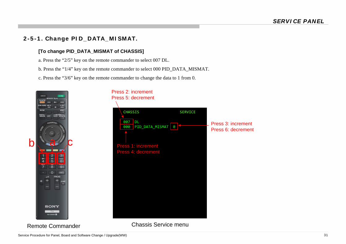
CHASSIS SERVICE
007 DL000 PID_DATA_MISMAT 0
Service Procedure for Panel, Board and Software Change / Upgrade(WW) 31
Chassis Service menu
Press 2: incrementPress 5: decrement
Press 1: incrementPress 4: decrement
Press 3: incrementPress 6: decrement
Remote Commander
ab c
[To change PID_DATA_MISMAT of CHASSIS]
a. Press the “2/5” key on the remote commander to select 007 DL.
b. Press the “1/4” key on the remote commander to select 000 PID_DATA_MISMAT.
c. Press the “3/6” key on the remote commander to change the data to 1 from 0.
2-5-1. Change PID_DATA_MISMAT.
SERVICE PANEL

Service Procedure for Panel, Board and Software Change / Upgrade(WW) 32
ab
Remote Commander
[To store data changed in “CHASSIS”]
a. Press “MUTING” on the remote commander. “SERVICE” will be changed to “WRITE” .
b. Press “0” on the remote commander.“WRITE” displayed in green on the screen is changed to “WRITE” displayed in red, and then back to “SERVICE”.
c. Power OFF ON by using the power button on TV or Remote Commander.The “PID_DATA_MISMAT” will be changed back to “0”. Please go back to page 28 and proceed next step.
2-5-2. How to Store Changed Data
SERVICE PANEL
CHASSIS SERVICE
007 DL000 PID_DATA_MISMAT 1
CHASSIS SERVICE
007 DL000 PID_DATA_MISMAT 1
CHASSIS WRITE
007 DL000 PID_DATA_MISMAT 1
CHASSIS WRITE
007 DL000 PID_DATA_MISMAT 1
Chassis Service menu

Service Procedure for Panel, Board and Software Change / Upgrade(WW) 33
a. Access Service Mode by pressing the buttons “DISPLAY 5ch Vol+ POWER” on the remote commander when TV in standby.
b. Press the OPTIONS key to go to the VPC Service menu. (There are 3 Service menus “DIGITAL” “CHASSIS” “VPC”)
2-6. Setting necessary items in the Service Menu
SERVICE PANEL
1
3
4
Remote Commander
2OPTIONS
Digital Service menu
VPC SERVICE000 DATA_COPY000 BU_TRANS 0
VPC Service menu
DIGITAL SERVICE
001 OP000 VERS ‐‐‐
<MAIN> <EXT>DM1.301JPA RF:01.05WF1.003W00AA WF:2.0.0.99DF1.001W00AA WF:0BYM1.010W00AA CAM:X.XXXDB2.105W00AA FD:XXXX(DM1.301W00AA)DD1.016W00AAWP0.521W00AA <PEM>MID:1C117081 PM1.012W00LUPID:04020000 PB1.000W00LUPNL: PL1.011J46LUXFDMR370NN0101 PD1.011J46LUXTUNER :ENABLE

Service Procedure for Panel, Board and Software Change / Upgrade(WW) 34
VPC SERVICE001 DATA_BAKUP000 BU_FLASH 0
VPC Service menu
Press 2: incrementPress 5: decrement
Press 1: incrementPress 4: decrement
Press 3: incrementPress 6: decrement
VPC SERVICE001 DATA_BAKUP000 BU_FLASH 2
DATA TRANSFER NG
VPC SERVICE001 DATA_BAKUP000 BU_FLASH 3
DATA TRANSFER SUCCESS
Remote Commander
ab c
[To BU_FLASH of VPC]
a. Press the “2/5” key on the remote commander to select 001 DATA_BAKUP.
b. Press the “1/4” key on the remote commander to select 000 BU_FLASH.
c. Press the “3/6” key on the remote commander to select from 0 to 1. Data transfer will be done in few seconds.
2-6-1. Selecting the BU_FLASH
SERVICE PANEL
This procedure is to copy W/B adjustment data in BA* board to T-con board on Panel.
NG
OK
Note: This procedure is necessary for KDL-**HX85* only.

Service Procedure for Panel, Board and Software Change / Upgrade(WW) 35
DIGITAL SERVICE
001 OP000 VERS ‐‐‐
<MAIN> <EXT>DM1.301JPA RF:01.05WF1.003W00AA WF:2.0.0.99DF1.001W00AA WF:0BYM1.010W00AA CAM:X.XXXDB2.105W00AA FD:XXXX(DM1.301W00AA)DD1.016W00AAWP0.521W00AA <PEM>MID:1C117081 PM1.012W00LUPID:04020000 PB1.000W00LUPNL: PL1.011J46LUXFDMR370NN0101 PD1.011J46LUXTUNER :ENABLE
Digital Service menu
a. After completing all the service adjustment changes, verify that the correct Model ID and Product ID displays in the Service menu.
b. Press the OPTIONS key to go to the Digital Service menu. (There are 3 Service menus “DIGITAL” “CHASSIS” “VPC”)
c. Verify the Software version, Model ID and Product ID are the correct. Please refer the appendix pages to verify the Model ID and Product ID.
2-6-2. Confirming the Software version, Model ID and Product ID
SERVICE PANEL
Product ID
Model ID
OPTIONS
Remote Commander
Software version

SELF CHECK
000 RESERVED ‐‐‐‐‐‐‐‐‐‐ ‐‐‐‐‐‐‐‐‐‐ ‐‐‐‐‐‐‐‐‐‐ 00000 RESERVED ‐‐‐‐‐‐‐‐‐‐ ‐‐‐‐‐‐‐‐‐‐ ‐‐‐‐‐‐‐‐‐‐ 00002 MAIN_POWE ‐‐‐‐‐‐‐‐‐‐ ‐‐‐‐‐‐‐‐‐‐ ‐‐‐‐‐‐‐‐‐‐ 00003 DC_ALERT ‐‐‐‐‐‐‐‐‐‐ ‐‐‐‐‐‐‐‐‐‐ ‐‐‐‐‐‐‐‐‐‐ 00003 AUD_PROT ‐‐‐‐‐‐‐‐‐‐ ‐‐‐‐‐‐‐‐‐‐ ‐‐‐‐‐‐‐‐‐‐ 00003 HDMI_EQ ‐‐‐‐‐‐‐‐‐‐ ‐‐‐‐‐‐‐‐‐‐ ‐‐‐‐‐‐‐‐‐‐ 00003 TU_DEMOD ‐‐‐‐‐‐‐‐‐‐ ‐‐‐‐‐‐‐‐‐‐ ‐‐‐‐‐‐‐‐‐‐ 00004 VLED ‐‐‐‐‐‐‐‐‐‐ ‐‐‐‐‐‐‐‐‐‐ ‐‐‐‐‐‐‐‐‐‐ 00004 LD_ERR ‐‐‐‐‐‐‐‐‐‐ ‐‐‐‐‐‐‐‐‐‐ ‐‐‐‐‐‐‐‐‐‐ 00005 HFR_ERR ‐‐‐‐‐‐‐‐‐‐ ‐‐‐‐‐‐‐‐‐‐ ‐‐‐‐‐‐‐‐‐‐ 00005 TCON_ERR ‐‐‐‐‐‐‐‐‐‐ ‐‐‐‐‐‐‐‐‐‐ ‐‐‐‐‐‐‐‐‐‐ 00005 P_ID_ERR ‐‐‐‐‐‐‐‐‐‐ ‐‐‐‐‐‐‐‐‐‐ ‐‐‐‐‐‐‐‐‐‐ 00006 BACKLITE ‐‐‐‐‐‐‐‐‐‐ ‐‐‐‐‐‐‐‐‐‐ ‐‐‐‐‐‐‐‐‐‐ 00007 TEMP_ERR ‐‐‐‐‐‐‐‐‐‐ ‐‐‐‐‐‐‐‐‐‐ ‐‐‐‐‐‐‐‐‐‐ 00007 FAN_ERR ‐‐‐‐‐‐‐‐‐‐ ‐‐‐‐‐‐‐‐‐‐ ‐‐‐‐‐‐‐‐‐‐ 00010 EMITTER ‐‐‐‐‐‐‐‐‐‐ ‐‐‐‐‐‐‐‐‐‐ ‐‐‐‐‐‐‐‐‐‐ 00101 VPC_WDT ‐‐‐‐‐‐‐‐‐‐ ‐‐‐‐‐‐‐‐‐‐ ‐‐‐‐‐‐‐‐‐‐ 00102 MEPS_WDT ‐‐‐‐‐‐‐‐‐‐ ‐‐‐‐‐‐‐‐‐‐ ‐‐‐‐‐‐‐‐‐‐ 00103 HOST_WDT ‐‐‐‐‐‐‐‐‐‐ ‐‐‐‐‐‐‐‐‐‐ ‐‐‐‐‐‐‐‐‐‐ 00104 STBY_WDT ‐‐‐‐‐‐‐‐‐‐ ‐‐‐‐‐‐‐‐‐‐ ‐‐‐‐‐‐‐‐‐‐ 00
12345‐67891‐23456
Service Procedure for Panel, Board and Software Change / Upgrade(WW) 36
Self Check screen
Panel Operation Time
1
3
4
Remote Commander
2b b
2-7. Resetting the Panel Operation Time
SERVICE PANEL
a. Access to Self Check screen by pressing the buttons “DISPLAY 5ch Vol- POWER” on the remote commander when TV in standby.
b. Press “7” “0” on the remote commander to clear the LCD Panel operation time.

Service Procedure for Panel, Board and Software Change / Upgrade(WW) 37
The upgrade process is complete and unplug the AC cord
2-8. Finish Operation
SERVICE PANEL

Service Procedure for Panel, Board and Software Change / Upgrade (WW) 38
END
9-888-510-01
English2011DL08-DataMade in Japan
© 2012. 4
Sony CorporationHome Entertainment
Business Group

Service Procedure for Panel, Board and Software Change / Upgrade(WW) 39
Procedure described in this Appendix should be applied after BA* Board exchange process.
CAUTION!!! This function is irreversible. If you disable tuner function by mistake, you need to replace to new BA* board in order to re-enable tuner.
- Preparation
- Pass Code is required for this function. Please refer the Technical Bulletin to get the Pass Code.
- USB memory which includes “EU_Tuner_Disable.dat” file in the root is required.
1-1. Scope and Notes
APPENDIX 1 - TUNER DISABLE FOR EUROPE B2B MODELS

Service Procedure for Panel, Board and Software Change / Upgrade(WW) 40
1-2. Procedure to Disable Tuner
APPENDIX 1
1. TV Power ON and Insert USB memory with “EU_Tuner_Disable.dat” fileTuner Disable Display appears
2. Enter Pass Code by numeric key of remote commander.* If invalid code is entered 3 times, need to close dialog and start again.
Tuner Disable
1 9 Enter Password CancelRETURN
The Tuner function will be disabled completely.and cannot be reverted back to enabled state.
Please enter pass code to disable the Tuner
Pass Code:
Tuner Disable
ExitRETURN
Tuner is disabled. Unplug AC cable and plug again.
OK
3. Press “Enter” of remote commander and unplug AC and plug again.
4. Confirm Status of Tuner Function (ENABLE/DISABLE)Access Service Mode by pressing the buttons when TV in Standby.“DISPLAY 5ch Vol+ POWER” on the remote commander.
5. Power OFF ON
6. Finish
Example
DIGITAL SERVICE
001 OP000 VERS ‐‐‐
<MAIN> <EXT>DM1.301JPA RF:01.05WF1.003W00AA WF:2.0.0.99DF1.001W00AA WF:0BYM1.010W00AA CAM:X.XXXDB2.105W00AA FD:XXXX(DM1.301W00AA)DD1.016W00AAWP0.521W00AA <PEM>MID:1C117081 PM1.012W00LUPID:04020000 PB1.000W00LUPNL: PL1.011J46LUXFDMR370NN0101 PD1.011J46LUXTUNER :DISABLE

Service Procedure for Panel, Board and Software Change / Upgrade(WW) 41
1-3. B2B Tuner Disable Model List
APPENDIX 1
- Tuner Disable function by USB memory is supported for EU-T and EU-T2 models.
- Available production models are only listed models. Please DO NOT use this feature for other models.
- Tuner Disable Display doesn’t appear on unsupported models.
Model Name Serial Number
KDL-55HX753 5,500,001-5,600,000
KDL-46EX653 5,500,001-5,600,000
KDL-40EX653 5,500,001-5,600,000
KDL-32EX653 1,300,001-1,400,000

Service Procedure for Panel, Board and Software Change / Upgrade(WW) 42
Procedure described in this Appendix should be applied after BA* Board exchange process for China Hotel Model (with RS232C Control).
By executing the procedure described in this Appendix, RS232C Control protocol will be set to “Sony Standard”. (Default setting of service board is “No Serial”.)
1-1. Scope and Notes
APPENDIX 2 - RS232C SETTING FOR CHINA HOTEL MODELS

Service Procedure for Panel, Board and Software Change / Upgrade(WW) 43
1-2. Procedure to Set HOTEL RS232C Protocol
APPENDIX 2
1. Access Service Mode by pressing the buttons when TV in Standby.“DISPLAY 5ch Vol+ POWER” on the remote commander.
2. Select [002 MODEL – 004 SHIP_CONFIRM]Press “1” button on the remote commander several times.
3. Enter to SHIP_CONFIRMPress “0” button on the remote commander.
Example
DIGITAL SERVICE
001 OP000 VERS ‐‐‐
<MAIN> <EXT>DM1.301JPA RF:01.05WF1.003W00AA WF:2.0.0.99DF1.001W00AA WF:0BYM1.010W00AA CAM:X.XXXDB2.105W00AA FD:XXXX(DM1.301W00AA)DD1.016W00AAWP0.521W00AA <PEM>MID:1C117081 PM1.012W00LUPID:04020000 PB1.000W00LUPNL: PL1.011J46LUXFDMR370NN0101 PD1.011J46LUXTUNER :ENABLE
DIGITAL SERVICE
002 MODEL004 SHIP_CONFIRM ‐‐‐
DIGITAL (MODEL) SERVICE
Confirmation for Shipping
4. Enter to Product Code Input MenuPress “+”(Select) button on the remote commander.
DIGITAL (MODEL) SERVICE
Confirmation for Shipping
Current ProductCodeP________Please input 8 digit ProductCode(00000000‐99999999)P________

Service Procedure for Panel, Board and Software Change / Upgrade(WW) 44
APPENDIX 2
5. Enter to Product Code Input MenuInput 8 digit of Product Code by remote commander and then press “+”(Select) button.*Please refer to the next page for the Product Code.
6. Confirm the completion of the process*Please refer to the next page for the Error Code (Result : 0xXXXX)
7. Power OFF ON
8. Finish (If you see an error code at step 6, go to step 1.)
DIGITAL (MODEL) SERVICE
Confirmation for Shipping
Current ProductCodeP________Please input 8 digit ProductCode(00000000‐99999999)P18494500
DIGITAL (MODEL) SERVICE
Confirmation for Shipping
P18494500 ProductCode you input
Done Completion Message

Service Procedure for Panel, Board and Software Change / Upgrade(WW) 45
1-3. China Hotel Model (with RS232C Control) Product Code and Error Code
APPENDIX 2
< Product Code >
Model Name Product Code Serial Number
KDL-55HX750 18493500
1,450,001-1,500,000
KDL-46HX750 18493600
KDL-40HX750 18494500
KDL-46EX650 18494600
KDL-40EX650 18494700
KDL-32EX650 18494800
KDL-32EX550 18494900
< Error Code >
Error Code Status
0x0001 Product Code input errorPlease confirm Product Code
0x0010 Need Software UpdatePlease update Software by USB0x0020
0x0040
0x0080

Service Procedure for Panel, Board and Software Change / Upgrade(WW) 46
Procedure described in this Appendix should be applied after BA* Board exchange process for GA Hotel Model (with RS232C Control) .
By executing the procedure described in this Appendix, RS232C Control protocol will be set to appropriate mode (Locatel/VDA/SonyStandard). (Default setting of service board is “No Serial”)
1-1. Scope and Notes
APPENDIX 3 - SI SELECTION SETTING FOR GA HOTEL MODELS

Service Procedure for Panel, Board and Software Change / Upgrade(WW) 47
1-2. Procedure to Set HOTEL RS232C Protocol
APPENDIX 3
1. Access Hotel Setting Mode by pressing the buttons when TV in Standby.“DISPLAY MUTING Vol+ POWER” on the remote commander.
2. Enter to [HOME] [Settings] [Hotel Mode] and select [SI mode selection]
3. Select appropriate protocol from the list.
Example
4. Power OFF ONHotel Mode Settings in process
Maximum Volume
Initial Volume
Line‐out Offset
SI mode selection
BathSP Initial Volume
Initialize Hotel Settings
Export Hotel Settings
Sony standardLocatelVDANo serial
Hotel Mode Settings in process
5. Confirm SI mode selection setting in [Settings]
6. Finish
< NOTE >• To exit Hotel Mode (for Guest), press the buttons when TV in Power ON.
“DISPLAY MUTING Vol+ Home” on the remote commander.• To exit Hotel Setting Mode, press the buttons when TV in Standby.
“DISPLAY MUTING Vol- POWER” on the remote commander.
• “Cloning” is also available for this Protocol setting.In case you use “Cloning” instead of this procedure, please check SI mode selection setting after “Cloning”.
• Reboot is required to activate this Protocol setting.
Normal Mode
Hotel Setting Mode Hotel Mode (for Guest)

Service Procedure for Panel, Board and Software Change / Upgrade(WW) 48
1-3. GA Hotel Model (with RS232C Control) Model List
APPENDIX 3
< Locatel/VDA Model List >
Model Name Serial Number
KDL-55HX750
3,020,001-3,030,000
KDL-46HX750
KDL-40HX750
KDL-46EX650
KDL-40EX650
KDL-32EX650

<Americas> <Americas>Model Name ProductCode Model-ID Product-ID Panel Name 000 SEG 001 DEST PKG Spec Model Name ProductCode Model-ID Product-ID Panel Name 000 SEG 001 DEST PKG SpecKDL-26EX555 18462000 4423A224 04047040 V260B3-LE2 P-2A_BASE ISDB-LTN_BASE BRA BR6 KDL-46EX657 18460300 1C23AC30 05047040 LTY460HN0701 P-2A_BASE DVB-LTN_BASE GAA CO1KDL-32EX550 18452502 1C23A122 03047040 LTY320AN0301 P-2A_BASE ATSC-LTN_BASE AAA LA1 KDL-46HX750 18451800 0D33A116 01042040 LTY460HQ0501 3a_BASE ATSC-UC_BASE AAA U2KDL-32EX550 18452502 1C23A12F 03047040 LTY320AN0501 P-2A_BASE ATSC-LTN_BASE AAA LA1 KDL-46HX750 18451800 0D33A116 01042040 LTY460HQ0502 3a_BASE ATSC-UC_BASE AAA U2KDL-32EX555 18456700 1C23A222 04187040 LTY320AN0301 P-2A_BASE ISDB-LTN_NO-GIN BRB CL3 KDL-46HX750 18451800 0D33A132 01042040 LTY460HQ0601 3a_BASE ATSC-UC_BASE AAA U2KDL-32EX555 18456700 1C23A22F 04187040 LTY320AN0501 P-2A_BASE ISDB-LTN_NO-GIN BRB CL3 KDL-46HX750 18451801 0D33A116 01042040 LTY460HQ0501 3a_BASE ATSC-UC_BASE AAA CA2KDL-32EX555 18461900 1C23A222 04047040 LTY320AN0301 P-2A_BASE ISDB-LTN_BASE BRA BR6 KDL-46HX750 18451801 0D33A116 01042040 LTY460HQ0502 3a_BASE ATSC-UC_BASE AAA CA2KDL-32EX555 18461900 1C23A22F 04047040 LTY320AN0501 P-2A_BASE ISDB-LTN_BASE BRA BR6 KDL-46HX750 18451801 0D33A132 01042040 LTY460HQ0601 3a_BASE ATSC-UC_BASE AAA CA2KDL-32EX555 18456701 1C23A222 04187040 LTY320AN0301 P-2A_BASE ISDB-LTN_NO-GIN BRB VZ2 KDL-46HX750 18451802 0C33A116 03042040 LTY460HQ0501 3a_BASE ATSC-LTN_BASE AAA LA1KDL-32EX555 18456701 1C23A22F 04187040 LTY320AN0501 P-2A_BASE ISDB-LTN_NO-GIN BRB VZ2 KDL-46HX750 18451802 0C33A116 03042040 LTY460HQ0502 3a_BASE ATSC-LTN_BASE AAA LA1KDL-32EX557 18460000 1C23AC22 05047040 LTY320AN0301 P-2A_BASE DVB-LTN_BASE GAA CO1 KDL-46HX750 18451802 0C33A132 03042040 LTY460HQ0601 3a_BASE ATSC-LTN_BASE AAA LA1KDL-32EX557 18460000 1C23AC2F 05047040 LTY320AN0501 P-2A_BASE DVB-LTN_BASE GAA CO1 KDL-46HX751 18496602 0C33A116 03042040 LTY460HQ0501 3a_BASE ATSC-LTN_BASE AAA LA1KDL-32EX650 18468602 1C23A125 03047040 LTY320HN0301 P-2A_BASE ATSC-LTN_BASE AAA LA1 KDL-46HX751 18496602 0C33A116 03042040 LTY460HQ0502 3a_BASE ATSC-LTN_BASE AAA LA1KDL-32EX651 18487802 1C23A125 03047040 LTY320HN0301 P-2A_BASE ATSC-LTN_BASE AAA LA1 KDL-46HX751 18496602 0C33A132 03042040 LTY460HQ0601 3a_BASE ATSC-LTN_BASE AAA LA1KDL-32EX655 18463800 1D23A225 04047040 LTY320HN0301 P-2A_BASE ISDB-LTN_BASE BRA AR4 KDL-46HX751 18496601 0D33A116 01042040 LTY460HQ0501 3a_BASE ATSC-UC_BASE AAA CA2KDL-32EX655 18468400 1C23A225 04047040 LTY320HN0301 P-2A_BASE ISDB-LTN_BASE BRA BR6 KDL-46HX751 18496601 0D33A116 01042040 LTY460HQ0502 3a_BASE ATSC-UC_BASE AAA CA2KDL-32EX655 18468700 1C23A225 04187040 LTY320HN0301 P-2A_BASE ISDB-LTN_NO-GIN BRB CL3 KDL-46HX751 18496601 0D33A132 01042040 LTY460HQ0601 3a_BASE ATSC-UC_BASE AAA CA2KDL-32EX655 18468701 1C23A225 04187040 LTY320HN0301 P-2A_BASE ISDB-LTN_NO-GIN BRB VZ2 KDL-46HX751 18496600 0D33A116 01042040 LTY460HQ0501 3a_BASE ATSC-UC_BASE AAA U2KDL-32EX655 18468410 1C23A225 04047040 LTY320HN0301 P-2A_BASE ISDB-LTN_BASE BRA BR6 KDL-46HX751 18496600 0D33A116 01042040 LTY460HQ0502 3a_BASE ATSC-UC_BASE AAA U2KDL-32EX657 18468800 1C23AC25 05047040 LTY320HN0301 P-2A_BASE DVB-LTN_BASE GAA CO1 KDL-46HX751 18496600 0D33A132 01042040 LTY460HQ0601 3a_BASE ATSC-UC_BASE AAA U2KDL-32HX750 18452002 0C33A121 03042040 LTY320HQ0101 3a_BASE ATSC-LTN_BASE AAA LA1 KDL-46HX752 18463600 0D33A216 040420C0 LTY460HQ0501 3a_WIFI_READY ISDB-LTN_BASE BRA AR4KDL-32HX750 18452002 0C33A121 03042040 LTY320HQ0102 3a_BASE ATSC-LTN_BASE AAA LA1 KDL-46HX752 18463600 0D33A216 040420C0 LTY460HQ0502 3a_WIFI_READY ISDB-LTN_BASE BRA AR4KDL-32HX755 18455900 0C33A221 04182040 LTY320HQ0101 3a_BASE ISDB-LTN_NO-GIN BRB CL3 KDL-46HX752 18463600 0D33A232 040420C0 LTY460HQ0601 3a_WIFI_READY ISDB-LTN_BASE BRA AR4KDL-32HX755 18455900 0C33A221 04182040 LTY320HQ0102 3a_BASE ISDB-LTN_NO-GIN BRB CL3 KDL-46HX755 18455700 0C33A216 04182040 LTY460HQ0501 3a_BASE ISDB-LTN_NO-GIN BRB CL3KDL-32HX755 18461600 0C33A221 04042040 LTY320HQ0101 3a_BASE ISDB-LTN_BASE BRA BR6 KDL-46HX755 18455700 0C33A216 04182040 LTY460HQ0502 3a_BASE ISDB-LTN_NO-GIN BRB CL3KDL-32HX755 18461600 0C33A221 04042040 LTY320HQ0102 3a_BASE ISDB-LTN_BASE BRA BR6 KDL-46HX755 18455700 0C33A232 04182040 LTY460HQ0601 3a_BASE ISDB-LTN_NO-GIN BRB CL3KDL-32HX755 18455901 0C33A221 04182040 LTY320HQ0101 3a_BASE ISDB-LTN_NO-GIN BRB VZ2 KDL-46HX755 18461400 0C33A216 04042040 LTY460HQ0501 3a_BASE ISDB-LTN_BASE BRA BR6KDL-32HX755 18455901 0C33A221 04182040 LTY320HQ0102 3a_BASE ISDB-LTN_NO-GIN BRB VZ2 KDL-46HX755 18461400 0C33A216 04042040 LTY460HQ0502 3a_BASE ISDB-LTN_BASE BRA BR6KDL-32HX757 18460700 0C33AC21 05042040 LTY320HQ0101 3a_BASE DVB-LTN_BASE GAA CO1 KDL-46HX755 18461400 0C33A232 04042040 LTY460HQ0601 3a_BASE ISDB-LTN_BASE BRA BR6KDL-32HX757 18460700 0C33AC21 05042040 LTY320HQ0102 3a_BASE DVB-LTN_BASE GAA CO1 KDL-46HX755 18455701 0C33A216 04182040 LTY460HQ0501 3a_BASE ISDB-LTN_NO-GIN BRB VZ2KDL-32NX655 18504700 1C53A228 04048040 FSLL320NT0101 P-2S_BASE ISDB-LTN_BASE BRA BR6 KDL-46HX755 18455701 0C33A216 04182040 LTY460HQ0502 3a_BASE ISDB-LTN_NO-GIN BRB VZ2KDL-40EX650 18468902 1C23A126 03047040 LTY400HM1001 P-2A_BASE ATSC-LTN_BASE AAA LA1 KDL-46HX755 18455701 0C33A232 04182040 LTY460HQ0601 3a_BASE ISDB-LTN_NO-GIN BRB VZ2KDL-40EX651 18487702 1C23A126 03047040 LTY400HM1001 P-2A_BASE ATSC-LTN_BASE AAA LA1 KDL-46HX757 18460900 0C33AC16 05042040 LTY460HQ0501 3a_BASE DVB-LTN_BASE GAA CO1KDL-40EX655 18463900 1D23A226 04047040 LTY400HM1001 P-2A_BASE ISDB-LTN_BASE BRA AR4 KDL-46HX757 18460900 0C33AC16 05042040 LTY460HQ0502 3a_BASE DVB-LTN_BASE GAA CO1KDL-40EX655 18468500 1C23A226 04047040 LTY400HM1001 P-2A_BASE ISDB-LTN_BASE BRA BR6 KDL-46HX757 18460900 0C33AC32 05042040 LTY460HQ0601 3a_BASE DVB-LTN_BASE GAA CO1KDL-40EX655 18469000 1C23A226 04187040 LTY400HM1001 P-2A_BASE ISDB-LTN_NO-GIN BRB CL3 KDL-46HX850 18451400 0543A11F 01041040 FQLR460LT0101 3a-G_BASE ATSC-UC_BASE AAA U2KDL-40EX655 18469001 1C23A226 04187040 LTY400HM1001 P-2A_BASE ISDB-LTN_NO-GIN BRB VZ2 KDL-46HX850 18451401 0543A11F 01041040 FQLR460LT0101 3a-G_BASE ATSC-UC_BASE AAA CA2KDL-40EX657 18469100 1C23AC26 05047040 LTY400HM1001 P-2A_BASE DVB-LTN_BASE GAA CO1 KDL-46HX850 18451402 0443A11F 03041040 FQLR460LT0101 3a-G_BASE ATSC-LTN_BASE AAA LA1KDL-40HX750 18451902 0C33A115 03042040 LTY400HL0401 3a_BASE ATSC-LTN_BASE AAA LA1 KDL-46HX855 18456200 0443A21F 04181040 FQLR460LT0101 3a-G_BASE ISDB-LTN_NO-GIN BRB CL3KDL-40HX750 18451902 0C33A115 03042040 LTY400HL0402 3a_BASE ATSC-LTN_BASE AAA LA1 KDL-46HX855 18461800 0443A21F 04041040 FQLR460LT0101 3a-G_BASE ISDB-LTN_BASE BRA BR6KDL-40HX750 18451902 0C33A131 03042040 LTY400HL0501 3a_BASE ATSC-LTN_BASE AAA LA1 KDL-46HX855 18456201 0443A21F 04181040 FQLR460LT0101 3a-G_BASE ISDB-LTN_NO-GIN BRB VZ2KDL-40HX752 18463700 0D33A215 040420C0 LTY400HL0401 3a_WIFI_READY ISDB-LTN_BASE BRA AR4 KDL-46HX857 18460500 0443AC1F 05041040 FQLR460LT0101 3a-G_BASE DVB-LTN_BASE GAA CO1KDL-40HX752 18463700 0D33A215 040420C0 LTY400HL0402 3a_WIFI_READY ISDB-LTN_BASE BRA AR4 KDL-55HX750 18451700 0D33A117 01042040 LTY550HQ0401 3a_BASE ATSC-UC_BASE AAA U2KDL-40HX752 18463700 0D33A231 040420C0 LTY400HL0501 3a_WIFI_READY ISDB-LTN_BASE BRA AR4 KDL-55HX750 18451700 0D33A133 01042040 LTY550HQ0501 3a_BASE ATSC-UC_BASE AAA U2KDL-40HX755 18455800 0C33A215 04182040 LTY400HL0401 3a_BASE ISDB-LTN_NO-GIN BRB CL3 KDL-55HX750 18451701 0D33A117 01042040 LTY550HQ0401 3a_BASE ATSC-UC_BASE AAA CA2KDL-40HX755 18455800 0C33A215 04182040 LTY400HL0402 3a_BASE ISDB-LTN_NO-GIN BRB CL3 KDL-55HX750 18451701 0D33A133 01042040 LTY550HQ0501 3a_BASE ATSC-UC_BASE AAA CA2KDL-40HX755 18455800 0C33A231 04182040 LTY400HL0501 3a_BASE ISDB-LTN_NO-GIN BRB CL3 KDL-55HX750 18451702 0C33A117 03042040 LTY550HQ0401 3a_BASE ATSC-LTN_BASE AAA LA1KDL-40HX755 18461500 0C33A215 04042040 LTY400HL0401 3a_BASE ISDB-LTN_BASE BRA BR6 KDL-55HX750 18451702 0C33A133 03042040 LTY550HQ0501 3a_BASE ATSC-LTN_BASE AAA LA1KDL-40HX755 18461500 0C33A215 04042040 LTY400HL0402 3a_BASE ISDB-LTN_BASE BRA BR6 KDL-55HX751 18487502 0C33A117 03042040 LTY550HQ0401 3a_BASE ATSC-LTN_BASE AAA LA1KDL-40HX755 18461500 0C33A231 04042040 LTY400HL0501 3a_BASE ISDB-LTN_BASE BRA BR6 KDL-55HX751 18487502 0C33A133 03042040 LTY550HQ0501 3a_BASE ATSC-LTN_BASE AAA LA1KDL-40HX755 18455801 0C33A215 04182040 LTY400HL0401 3a_BASE ISDB-LTN_NO-GIN BRB VZ2 KDL-55HX751 18487501 0D33A117 01042040 LTY550HQ0401 3a_BASE ATSC-UC_BASE AAA CA2KDL-40HX755 18455801 0C33A215 04182040 LTY400HL0402 3a_BASE ISDB-LTN_NO-GIN BRB VZ2 KDL-55HX751 18487501 0D33A133 01042040 LTY550HQ0501 3a_BASE ATSC-UC_BASE AAA CA2KDL-40HX755 18455801 0C33A231 04182040 LTY400HL0501 3a_BASE ISDB-LTN_NO-GIN BRB VZ2 KDL-55HX751 18487500 0D33A117 01042040 LTY550HQ0401 3a_BASE ATSC-UC_BASE AAA U2KDL-40HX757 18460800 0C33AC15 05042040 LTY400HL0401 3a_BASE DVB-LTN_BASE GAA CO1 KDL-55HX751 18487500 0D33A133 01042040 LTY550HQ0501 3a_BASE ATSC-UC_BASE AAA U2KDL-40HX757 18460800 0C33AC15 05042040 LTY400HL0402 3a_BASE DVB-LTN_BASE GAA CO1 KDL-55HX755 18455600 0C33A217 04182040 LTY550HQ0401 3a_BASE ISDB-LTN_NO-GIN BRB CL3KDL-40HX757 18460800 0C33AC31 05042040 LTY400HL0501 3a_BASE DVB-LTN_BASE GAA CO1 KDL-55HX755 18455600 0C33A233 04182040 LTY550HQ0501 3a_BASE ISDB-LTN_NO-GIN BRB CL3KDL-40NX655 18504800 1C53A229 04048040 FSLL400NT0101 P-2S_BASE ISDB-LTN_BASE BRA BR6 KDL-55HX755 18461300 0C33A217 04042040 LTY550HQ0401 3a_BASE ISDB-LTN_BASE BRA BR6KDL-46EX650 18471302 1C23A127 03047040 LTY460HN0501 P-2A_BASE ATSC-LTN_BASE AAA LA1 KDL-55HX755 18461300 0C33A233 04042040 LTY550HQ0501 3a_BASE ISDB-LTN_BASE BRA BR6KDL-46EX650 18471302 1C23A130 03047040 LTY460HN0701 P-2A_BASE ATSC-LTN_BASE AAA LA1 KDL-55HX755 18455601 0C33A217 04182040 LTY550HQ0401 3a_BASE ISDB-LTN_NO-GIN BRB VZ2KDL-46EX651 18487602 1C23A127 03047040 LTY460HN0501 P-2A_BASE ATSC-LTN_BASE AAA LA1 KDL-55HX755 18455601 0C33A233 04182040 LTY550HQ0501 3a_BASE ISDB-LTN_NO-GIN BRB VZ2KDL-46EX651 18487602 1C23A130 03047040 LTY460HN0701 P-2A_BASE ATSC-LTN_BASE AAA LA1 KDL-55HX757 18461000 0C33AC17 05042040 LTY550HQ0401 3a_BASE DVB-LTN_BASE GAA CO1KDL-46EX655 18456400 1C23A227 04187040 LTY460HN0501 P-2A_BASE ISDB-LTN_NO-GIN BRB CL3 KDL-55HX757 18461000 0C33AC33 05042040 LTY550HQ0501 3a_BASE DVB-LTN_BASE GAA CO1KDL-46EX655 18456400 1C23A230 04187040 LTY460HN0701 P-2A_BASE ISDB-LTN_NO-GIN BRB CL3 KDL-55HX850 18451300 0543A120 01041040 FQLR550LT0101 3a-G_BASE ATSC-UC_BASE AAA U2KDL-46EX655 18471200 1C23A227 04047040 LTY460HN0501 P-2A_BASE ISDB-LTN_BASE BRA BR6 KDL-55HX850 18451300 0543A135 01041040 FQLR550LT0102 3a-G_BASE ATSC-UC_BASE AAA U2KDL-46EX655 18471200 1C23A230 04047040 LTY460HN0701 P-2A_BASE ISDB-LTN_BASE BRA BR6 KDL-55HX850 18451301 0543A120 01041040 FQLR550LT0101 3a-G_BASE ATSC-UC_BASE AAA CA2KDL-46EX655 18456401 1C23A227 04187040 LTY460HN0501 P-2A_BASE ISDB-LTN_NO-GIN BRB VZ2 KDL-55HX850 18451301 0543A135 01041040 FQLR550LT0102 3a-G_BASE ATSC-UC_BASE AAA CA2KDL-46EX655 18456401 1C23A230 04187040 LTY460HN0701 P-2A_BASE ISDB-LTN_NO-GIN BRB VZ2 KDL-55HX850 18451302 0443A120 03041040 FQLR550LT0101 3a-G_BASE ATSC-LTN_BASE AAA LA1KDL-46EX657 18460300 1C23AC27 05047040 LTY460HN0501 P-2A_BASE DVB-LTN_BASE GAA CO1 KDL-55HX850 18451302 0443A135 03041040 FQLR550LT0102 3a-G_BASE ATSC-LTN_BASE AAA LA1
Appendix 4 - Model ID / Product ID and Panel Information

<Americas> <Asia>Model Name ProductCode Model-ID Product-ID Panel Name 000 SEG 001 DEST PKG Spec Model Name ProductCode Model-ID Product-ID Panel Name 000 SEG 001 DEST PKG SpecKDL-55HX855 18456100 0443A220 04181040 FQLR550LT0101 3a-G_BASE ISDB-LTN_NO-GIN BRB CL3 KDL-26EX550 18442600 4423A424 08047040 V260B3-LE2 P-2A_BASE DTMB-HK_BASE GAA HK5KDL-55HX855 18456100 0443A235 04181040 FQLR550LT0102 3a-G_BASE ISDB-LTN_NO-GIN BRB CL3 KDL-26EX550 18470701 4523A524 090C7040 V260B3-LE2 P-2A_BASE DVB-GA-T_NO-NU GAA IN5KDL-55HX855 18461700 0443A220 04041040 FQLR550LT0101 3a-G_BASE ISDB-LTN_BASE BRA BR6 KDL-26EX550 18470706 4423A524 090C7040 V260B3-LE2 P-2A_BASE DVB-GA-T_NO-NU GAA AU5KDL-55HX855 18461700 0443A235 04041040 FQLR550LT0102 3a-G_BASE ISDB-LTN_BASE BRA BR6 KDL-32EX550 18442500 1C23A422 08047040 LTY320AN0301 P-2A_BASE DTMB-HK_BASE GAA HK5KDL-55HX855 18456101 0443A220 04181040 FQLR550LT0101 3a-G_BASE ISDB-LTN_NO-GIN BRB VZ2 KDL-32EX550 18442500 1C23A42F 08047040 LTY320AN0501 P-2A_BASE DTMB-HK_BASE GAA HK5KDL-55HX855 18456101 0443A235 04181040 FQLR550LT0102 3a-G_BASE ISDB-LTN_NO-GIN BRB VZ2 KDL-32EX550 18470601 1D23A522 090C7040 LTY320AN0301 P-2A_BASE DVB-GA-T_NO-NU GAA IN5KDL-55HX857 18460600 0443AC20 05041040 FQLR550LT0101 3a-G_BASE DVB-LTN_BASE GAA CO1 KDL-32EX550 18470601 1D23A52F 090C7040 LTY320AN0501 P-2A_BASE DVB-GA-T_NO-NU GAA IN5KDL-55HX857 18460600 0443AC35 05041040 FQLR550LT0102 3a-G_BASE DVB-LTN_BASE GAA CO1 KDL-32EX650 18468100 1C23A325 06047040 LTY320HN0301 P-2A_BASE DVB-TW_BASE GAA TW6
KDL-32EX650 18468300 1C23A425 08047040 LTY320HN0301 P-2A_BASE DTMB-HK_BASE GAA HK5KDL-32EX650 18470500 1D23A525 09047040 LTY320HN0301 P-2A_BASE DVB-GA-T_BASE GAA ME6KDL-32EX650 18470501 1D23A525 090C7040 LTY320HN0301 P-2A_BASE DVB-GA-T_NO-NU GAA IN5KDL-32EX650 18470506 1C23A525 090C7040 LTY320HN0301 P-2A_BASE DVB-GA-T_NO-NU GAA AU5KDL-32EX650 18470505 1D23A525 090C7040 LTY320HN0301 P-2A_BASE DVB-GA-T_NO-NU GAA SA2KDL-32EX650 18470502 1D23A525 09047040 LTY320HN0301 P-2A_BASE DVB-GA-T_BASE GAA TH8KDL-32EX650 18470503 1D23A525 09047040 LTY320HN0301 P-2A_BASE DVB-GA-T_BASE GAA MY1KDL-32EX650 18470504 1D23A525 090C7040 LTY320HN0301 P-2A_BASE DVB-GA-T_NO-NU GAA EA4KDL-32EX650 18493300 1D73A525 09047040 LTY320HN0301 P-2A_BASE DVB-GA-T_BASE GAA ME6KDL-32EX650 18502300 1D23A525 09047040 LTY320HN0301 P-2A_BASE DVB-GA-T_BASE GAA IR2KDL-32EX650 18502400 1D23A525 09047040 LTY320HN0301 P-2A_BASE DVB-GA-T_BASE GAA EG2KDL-32EX650 18502500 1D23A525 09047040 LTY320HN0301 P-2A_BASE DVB-GA-T_BASE GAA PK1KDL-32EX653 18495100 1D23A525 09107040 LTY320HN0301 P-2A_BASE DVB-GA-T_NO-SKNU GAB KW1KDL-32HX750 18433100 0D33A521 09042040 LTY320HQ0101 3a_BASE DVB-GA-T_BASE GAA ME6KDL-32HX750 18433100 0D33A521 09042040 LTY320HQ0102 3a_BASE DVB-GA-T_BASE GAA ME6KDL-32HX750 18437500 0C33A121 02042040 LTY320HQ0101 3a_BASE ATSC-KR_BASE AAA KR2KDL-32HX750 18437500 0C33A121 02042040 LTY320HQ0102 3a_BASE ATSC-KR_BASE AAA KR2KDL-32HX750 18439100 0C33A321 06042040 LTY320HQ0101 3a_BASE DVB-TW_BASE GAA TW6KDL-32HX750 18439100 0C33A321 06042040 LTY320HQ0102 3a_BASE DVB-TW_BASE GAA TW6KDL-32HX750 18440700 0C33A421 08042040 LTY320HQ0101 3a_BASE DTMB-HK_BASE GAA HK5KDL-32HX750 18440700 0C33A421 08042040 LTY320HQ0102 3a_BASE DTMB-HK_BASE GAA HK5KDL-32HX750 18433101 0D33A521 090C2040 LTY320HQ0101 3a_BASE DVB-GA-T_NO-NU GAA IN5KDL-32HX750 18433101 0D33A521 090C2040 LTY320HQ0102 3a_BASE DVB-GA-T_NO-NU GAA IN5KDL-32HX750 18433106 0C33A521 090C2040 LTY320HQ0101 3a_BASE DVB-GA-T_NO-NU GAA AU5KDL-32HX750 18433106 0C33A521 090C2040 LTY320HQ0102 3a_BASE DVB-GA-T_NO-NU GAA AU5KDL-32HX750 18433105 0D33A521 090C2040 LTY320HQ0101 3a_BASE DVB-GA-T_NO-NU GAA SA2KDL-32HX750 18433105 0D33A521 090C2040 LTY320HQ0102 3a_BASE DVB-GA-T_NO-NU GAA SA2KDL-32HX750 18433104 0D33A521 090C2040 LTY320HQ0101 3a_BASE DVB-GA-T_NO-NU GAA EA4KDL-32HX750 18433104 0D33A521 090C2040 LTY320HQ0102 3a_BASE DVB-GA-T_NO-NU GAA EA4KDL-32HX750 18433102 0D33A521 09042040 LTY320HQ0101 3a_BASE DVB-GA-T_BASE GAA TH8KDL-32HX750 18433102 0D33A521 09042040 LTY320HQ0102 3a_BASE DVB-GA-T_BASE GAA TH8KDL-32HX753 18495900 0D33A521 09102040 LTY320HQ0101 3a_BASE DVB-GA-T_NO-SKNU GAB KW1KDL-32HX753 18495900 0D33A521 09102040 LTY320HQ0102 3a_BASE DVB-GA-T_NO-SKNU GAB KW1KDL-32HX75A 18471100 0C33A421 080420C0 LTY320HQ0101 3a_WIFI_READY DTMB-HK_BASE GAA HK5KDL-32HX75A 18471100 0C33A421 080420C0 LTY320HQ0102 3a_WIFI_READY DTMB-HK_BASE GAA HK5KDL-32NX650 18504600 1D53A528 09048040 FSLL320NT0101 P-2S_BASE DVB-GA-T_BASE GAA AF1KDL-32NX650 18504604 1D53A528 090C8040 FSLL320NT0101 P-2S_BASE DVB-GA-T_NO-NU GAA EA4KDL-32NX650 18504601 1D53A528 090C8040 FSLL320NT0101 P-2S_BASE DVB-GA-T_NO-NU GAA IN5KDL-32NX650 18504606 1C53A528 090C8040 FSLL320NT0101 P-2S_BASE DVB-GA-T_NO-NU GAA AU5KDL-32NX653 18504400 1D53A528 09108040 FSLL320NT0101 P-2S_BASE DVB-GA-T_NO-SKNU GAB KW1KDL-40EX650 18468000 1C23A326 06047040 LTY400HM1001 P-2A_BASE DVB-TW_BASE GAA TW6KDL-40EX650 18468200 1C23A426 08047040 LTY400HM1001 P-2A_BASE DTMB-HK_BASE GAA HK5KDL-40EX650 18470400 1D23A526 09047040 LTY400HM1001 P-2A_BASE DVB-GA-T_BASE GAA ME6KDL-40EX650 18470401 1D23A526 090C7040 LTY400HM1001 P-2A_BASE DVB-GA-T_NO-NU GAA IN5KDL-40EX650 18470406 1C23A526 090C7040 LTY400HM1001 P-2A_BASE DVB-GA-T_NO-NU GAA AU5KDL-40EX650 18470405 1D23A526 090C7040 LTY400HM1001 P-2A_BASE DVB-GA-T_NO-NU GAA SA2KDL-40EX650 18470402 1D23A526 09047040 LTY400HM1001 P-2A_BASE DVB-GA-T_BASE GAA TH8KDL-40EX650 18470403 1D23A526 09047040 LTY400HM1001 P-2A_BASE DVB-GA-T_BASE GAA MY1KDL-40EX650 18470404 1D23A526 090C7040 LTY400HM1001 P-2A_BASE DVB-GA-T_NO-NU GAA EA4KDL-40EX650 18493200 1D73A526 09047040 LTY400HM1001 P-2A_BASE DVB-GA-T_BASE GAA ME6KDL-40EX650 18501800 1D23A526 09047040 LTY400HM1001 P-2A_BASE DVB-GA-T_BASE GAA IR2KDL-40EX650 18501900 1D23A526 09047040 LTY400HM1001 P-2A_BASE DVB-GA-T_BASE GAA EG2KDL-40EX650 18502000 1D23A526 09047040 LTY400HM1001 P-2A_BASE DVB-GA-T_BASE GAA PK1KDL-40EX650 18502100 1D23A526 09047040 LTY400HM1001 P-2A_BASE DVB-GA-T_BASE GAA SA1KDL-40EX650 18502200 1D23A526 09047040 LTY400HM1001 P-2A_BASE DVB-GA-T_BASE GAA E41KDL-40EX653 18495200 1D23A526 09107040 LTY400HM1001 P-2A_BASE DVB-GA-T_NO-SKNU GAB KW1KDL-40EX653 18495203 1D23A526 091C7040 LTY400HM1001 P-2A_BASE DVB-GA-T_NO-SKY GAB MY1KDL-40EX65A 18514703 1D23A526 09047040 LTY400HM1001 P-2A_BASE DVB-GA-T_BASE GAA MY1KDL-40HX750 18433000 0D33A515 09042040 LTY400HL0401 3a_BASE DVB-GA-T_BASE GAA ME6
Appendix 4 - Model ID / Product ID and Panel Information

<Asia> <Asia>Model Name ProductCode Model-ID Product-ID Panel Name 000 SEG 001 DEST PKG Spec Model Name ProductCode Model-ID Product-ID Panel Name 000 SEG 001 DEST PKG SpecKDL-40HX750 18433000 0D33A515 09042040 LTY400HL0402 3a_BASE DVB-GA-T_BASE GAA ME6 KDL-40NX650 18504504 1D53A529 090C8040 FSLL400NT0101 P-2S_BASE DVB-GA-T_NO-NU GAA EA4KDL-40HX750 18433000 0D33A531 09042040 LTY400HL0501 3a_BASE DVB-GA-T_BASE GAA ME6 KDL-40NX650 18504501 1D53A529 090C8040 FSLL400NT0101 P-2S_BASE DVB-GA-T_NO-NU GAA IN5KDL-40HX750 18437400 0C33A115 02042040 LTY400HL0401 3a-G_BASE ATSC-KR_BASE AAA KR2 KDL-40NX653 18504300 1D53A529 09108040 FSLL400NT0101 P-2S_BASE DVB-GA-T_NO-SKNU GAB KW1KDL-40HX750 18437400 0C33A115 02042040 LTY400HL0402 3a-G_BASE ATSC-KR_BASE AAA KR2 KDL-46EX650 18470300 1D23A527 09047040 LTY460HN0501 P-2A_BASE DVB-GA-T_BASE GAA ME6KDL-40HX750 18437400 0C33A131 02042040 LTY400HL0501 3a_BASE ATSC-KR_BASE AAA KR2 KDL-46EX650 18470300 1D23A530 09047040 LTY460HN0701 P-2A_BASE DVB-GA-T_BASE GAA ME6KDL-40HX750 18439000 0C33A315 06042040 LTY400HL0401 3a_BASE DVB-TW_BASE GAA TW6 KDL-46EX650 18470301 1D23A527 090C7040 LTY460HN0501 P-2A_BASE DVB-GA-T_NO-NU GAA IN5KDL-40HX750 18439000 0C33A315 06042040 LTY400HL0402 3a_BASE DVB-TW_BASE GAA TW6 KDL-46EX650 18470301 1D23A530 090C7040 LTY460HN0701 P-2A_BASE DVB-GA-T_NO-NU GAA IN5KDL-40HX750 18439000 0C33A331 06042040 LTY400HL0501 3a_BASE DVB-TW_BASE GAA TW6 KDL-46EX650 18470306 1C23A527 090C7040 LTY460HN0501 P-2A_BASE DVB-GA-T_NO-NU GAA AU5KDL-40HX750 18440600 0C33A415 08042040 LTY400HL0401 3a_BASE DTMB-HK_BASE GAA HK5 KDL-46EX650 18470306 1C23A530 090C7040 LTY460HN0701 P-2A_BASE DVB-GA-T_NO-NU GAA AU5KDL-40HX750 18440600 0C33A415 08042040 LTY400HL0402 3a_BASE DTMB-HK_BASE GAA HK5 KDL-46EX650 18489100 1C23A327 06047040 LTY460HN0501 P-2A_BASE DVB-TW_BASE GAA TW6KDL-40HX750 18440600 0C33A431 08042040 LTY400HL0501 3a_BASE DTMB-HK_BASE GAA HK5 KDL-46EX650 18489100 1C23A330 06047040 LTY460HN0701 P-2A_BASE DVB-TW_BASE GAA TW6KDL-40HX750 18433001 0D33A515 090C2040 LTY400HL0401 3a_BASE DVB-GA-T_NO-NU GAA IN5 KDL-46EX650 18470305 1D23A527 090C7040 LTY460HN0501 P-2A_BASE DVB-GA-T_NO-NU GAA SA2KDL-40HX750 18433001 0D33A515 090C2040 LTY400HL0402 3a_BASE DVB-GA-T_NO-NU GAA IN5 KDL-46EX650 18470305 1D23A530 090C7040 LTY460HN0701 P-2A_BASE DVB-GA-T_NO-NU GAA SA2KDL-40HX750 18433001 0D33A531 090C2040 LTY400HL0501 3a_BASE DVB-GA-T_NO-NU GAA IN5 KDL-46EX650 18470302 1D23A527 09047040 LTY460HN0501 P-2A_BASE DVB-GA-T_BASE GAA TH8KDL-40HX750 18433006 0C33A515 090C2040 LTY400HL0401 3a_BASE DVB-GA-T_NO-NU GAA AU5 KDL-46EX650 18470302 1D23A530 09047040 LTY460HN0701 P-2A_BASE DVB-GA-T_BASE GAA TH8KDL-40HX750 18433006 0C33A515 090C2040 LTY400HL0402 3a_BASE DVB-GA-T_NO-NU GAA AU5 KDL-46EX650 18470303 1D23A527 09047040 LTY460HN0501 P-2A_BASE DVB-GA-T_BASE GAA MY1KDL-40HX750 18433006 0C33A531 090C2040 LTY400HL0501 3a_BASE DVB-GA-T_NO-NU GAA AU5 KDL-46EX650 18470303 1D23A530 09047040 LTY460HN0701 P-2A_BASE DVB-GA-T_BASE GAA MY1KDL-40HX750 18433005 0D33A515 090C2040 LTY400HL0401 3a_BASE DVB-GA-T_NO-NU GAA SA2 KDL-46EX650 18470304 1D23A527 090C7040 LTY460HN0501 P-2A_BASE DVB-GA-T_NO-NU GAA EA4KDL-40HX750 18433005 0D33A515 090C2040 LTY400HL0402 3a_BASE DVB-GA-T_NO-NU GAA SA2 KDL-46EX650 18470304 1D23A530 090C7040 LTY460HN0701 P-2A_BASE DVB-GA-T_NO-NU GAA EA4KDL-40HX750 18433005 0D33A531 090C2040 LTY400HL0501 3a_BASE DVB-GA-T_NO-NU GAA SA2 KDL-46EX650 18493100 1D73A527 09047040 LTY460HN0501 P-2A_BASE DVB-GA-T_BASE GAA ME6KDL-40HX750 18433004 0D33A515 090C2040 LTY400HL0401 3a_BASE DVB-GA-T_NO-NU GAA EA4 KDL-46EX650 18493100 1D73A530 09047040 LTY460HN0701 P-2A_BASE DVB-GA-T_BASE GAA ME6KDL-40HX750 18433004 0D33A515 090C2040 LTY400HL0402 3a_BASE DVB-GA-T_NO-NU GAA EA4 KDL-46EX650 18501400 1D23A527 09047040 LTY460HN0501 P-2A_BASE DVB-GA-T_BASE GAA IR2KDL-40HX750 18433004 0D33A531 090C2040 LTY400HL0501 3a_BASE DVB-GA-T_NO-NU GAA EA4 KDL-46EX650 18501400 1D23A530 09047040 LTY460HN0701 P-2A_BASE DVB-GA-T_BASE GAA IR2KDL-40HX750 18433002 0D33A515 09042040 LTY400HL0401 3a_BASE DVB-GA-T_BASE GAA TH8 KDL-46EX650 18501500 1D23A527 09047040 LTY460HN0501 P-2A_BASE DVB-GA-T_BASE GAA EG2KDL-40HX750 18433002 0D33A515 09042040 LTY400HL0402 3a_BASE DVB-GA-T_BASE GAA TH8 KDL-46EX650 18501500 1D23A530 09047040 LTY460HN0701 P-2A_BASE DVB-GA-T_BASE GAA EG2KDL-40HX750 18433002 0D33A531 09042040 LTY400HL0501 3a_BASE DVB-GA-T_BASE GAA TH8 KDL-46EX650 18501600 1D23A527 09047040 LTY460HN0501 P-2A_BASE DVB-GA-T_BASE GAA PK1KDL-40HX750 18433003 0D33A515 09042040 LTY400HL0401 3a_BASE DVB-GA-T_BASE GAA MY1 KDL-46EX650 18501600 1D23A530 09047040 LTY460HN0701 P-2A_BASE DVB-GA-T_BASE GAA PK1KDL-40HX750 18433003 0D33A515 09042040 LTY400HL0402 3a_BASE DVB-GA-T_BASE GAA MY1 KDL-46EX650 18501700 1D23A527 09047040 LTY460HN0501 P-2A_BASE DVB-GA-T_BASE GAA SA1KDL-40HX750 18433003 0D33A531 09042040 LTY400HL0501 3a_BASE DVB-GA-T_BASE GAA MY1 KDL-46EX650 18501700 1D23A530 09047040 LTY460HN0701 P-2A_BASE DVB-GA-T_BASE GAA SA1KDL-40HX750 18493000 0D83A515 09042040 LTY400HL0401 3a_BASE DVB-GA-T_BASE GAA ME6 KDL-46EX653 18495300 1D23A527 09107040 LTY460HN0501 P-2A_BASE DVB-GA-T_NO-SKNU GAB KW1KDL-40HX750 18493000 0D83A515 09042040 LTY400HL0402 3a_BASE DVB-GA-T_BASE GAA ME6 KDL-46EX653 18495300 1D23A530 09107040 LTY460HN0701 P-2A_BASE DVB-GA-T_NO-SKNU GAB KW1KDL-40HX750 18493000 0D83A531 09042040 LTY400HL0501 3a_BASE DVB-GA-T_BASE GAA ME6 KDL-46EX653 18495303 1D23A527 091C7040 LTY460HN0501 P-2A_BASE DVB-GA-T_NO-SKY GAB MY1KDL-40HX750 18500800 0D33A515 09042040 LTY400HL0401 3a_BASE DVB-GA-T_BASE GAA IR2 KDL-46EX653 18495303 1D23A530 091C7040 LTY460HN0701 P-2A_BASE DVB-GA-T_NO-SKY GAB MY1KDL-40HX750 18500800 0D33A515 09042040 LTY400HL0402 3a_BASE DVB-GA-T_BASE GAA IR2 KDL-46EX65A 18514603 1D23A527 09047040 LTY460HN0501 P-2A_BASE DVB-GA-T_BASE GAA MY1KDL-40HX750 18500800 0D33A531 09042040 LTY400HL0501 3a_BASE DVB-GA-T_BASE GAA IR2 KDL-46EX65A 18514603 1D23A530 09047040 LTY460HN0701 P-2A_BASE DVB-GA-T_BASE GAA MY1KDL-40HX750 18500900 0D33A515 09042040 LTY400HL0401 3a_BASE DVB-GA-T_BASE GAA PK1 KDL-46HX750 18432900 0D33A516 09042040 LTY460HQ0501 3a-G_BASE DVB-GA-T_BASE GAA ME6KDL-40HX750 18500900 0D33A515 09042040 LTY400HL0402 3a_BASE DVB-GA-T_BASE GAA PK1 KDL-46HX750 18432900 0D33A516 09042040 LTY460HQ0502 3a-G_BASE DVB-GA-T_BASE GAA ME6KDL-40HX750 18500900 0D33A531 09042040 LTY400HL0501 3a_BASE DVB-GA-T_BASE GAA PK1 KDL-46HX750 18432900 0D33A532 09042040 LTY460HQ0601 3a_BASE DVB-GA-T_BASE GAA ME6KDL-40HX750 18501000 0D33A515 09042040 LTY400HL0401 3a_BASE DVB-GA-T_BASE GAA SA1 KDL-46HX750 18437300 0C33A116 02042040 LTY460HQ0501 3a_BASE ATSC-KR_BASE AAA KR2KDL-40HX750 18501000 0D33A515 09042040 LTY400HL0402 3a_BASE DVB-GA-T_BASE GAA SA1 KDL-46HX750 18437300 0C33A116 02042040 LTY460HQ0502 3a_BASE ATSC-KR_BASE AAA KR2KDL-40HX750 18501000 0D33A531 09042040 LTY400HL0501 3a_BASE DVB-GA-T_BASE GAA SA1 KDL-46HX750 18437300 0C33A132 02042040 LTY460HQ0601 3a_BASE ATSC-KR_BASE AAA KR2KDL-40HX753 18496200 0D33A515 09102040 LTY400HL0401 3a_BASE DVB-GA-T_NO-SKNU GAB KW1 KDL-46HX750 18438900 0C33A316 06042040 LTY460HQ0501 3a_BASE DVB-TW_BASE GAA TW6KDL-40HX753 18496200 0D33A515 09102040 LTY400HL0402 3a_BASE DVB-GA-T_NO-SKNU GAB KW1 KDL-46HX750 18438900 0C33A316 06042040 LTY460HQ0502 3a_BASE DVB-TW_BASE GAA TW6KDL-40HX753 18496200 0D33A531 09102040 LTY400HL0501 3a_BASE DVB-GA-T_NO-SKNU GAB KW1 KDL-46HX750 18438900 0C33A332 06042040 LTY460HQ0601 3a_BASE DVB-TW_BASE GAA TW6KDL-40HX75A 18470900 0C33A315 060420C0 LTY400HL0401 3a_WIFI_READY DVB-TW_BASE GAA TW6 KDL-46HX750 18440500 0C33A416 08042040 LTY460HQ0501 3a_BASE DTMB-HK_BASE GAA HK5KDL-40HX75A 18470900 0C33A315 060420C0 LTY400HL0402 3a_WIFI_READY DVB-TW_BASE GAA TW6 KDL-46HX750 18440500 0C33A416 08042040 LTY460HQ0502 3a_BASE DTMB-HK_BASE GAA HK5KDL-40HX75A 18470900 0C33A331 060420C0 LTY400HL0501 3a_WIFI_READY DVB-TW_BASE GAA TW6 KDL-46HX750 18440500 0C33A432 08042040 LTY460HQ0601 3a_BASE DTMB-HK_BASE GAA HK5KDL-40HX75A 18471000 0C33A415 080420C0 LTY400HL0401 3a_WIFI_READY DTMB-HK_BASE GAA HK5 KDL-46HX750 18432901 0D33A516 090C2040 LTY460HQ0501 3a_BASE DVB-GA-T_NO-NU GAA IN5KDL-40HX75A 18471000 0C33A415 080420C0 LTY400HL0402 3a_WIFI_READY DTMB-HK_BASE GAA HK5 KDL-46HX750 18432901 0D33A516 090C2040 LTY460HQ0502 3a_BASE DVB-GA-T_NO-NU GAA IN5KDL-40HX75A 18471000 0C33A431 080420C0 LTY400HL0501 3a_WIFI_READY DTMB-HK_BASE GAA HK5 KDL-46HX750 18432901 0D33A532 090C2040 LTY460HQ0601 3a_BASE DVB-GA-T_NO-NU GAA IN5KDL-40HX850 18437000 0443A11E 02041040 FQLR400LT0101 3a-G_BASE ATSC-KR_BASE AAA KR2 KDL-46HX750 18432906 0C33A516 090C2040 LTY460HQ0501 3a_BASE DVB-GA-T_NO-NU GAA AU5KDL-40HX850 18437000 0443A134 02041040 FQLR400LT0102 3a-G_BASE ATSC-KR_BASE AAA KR2 KDL-46HX750 18432906 0C33A516 090C2040 LTY460HQ0502 3a_BASE DVB-GA-T_NO-NU GAA AU5KDL-40HX850 18440200 0443A41E 08041040 FQLR400LT0101 3a-G_BASE DTMB-HK_BASE GAA HK5 KDL-46HX750 18432906 0C33A532 090C2040 LTY460HQ0601 3a_BASE DVB-GA-T_NO-NU GAA AU5KDL-40HX850 18440200 0443A434 08041040 FQLR400LT0102 3a-G_BASE DTMB-HK_BASE GAA HK5 KDL-46HX750 18432905 0D33A516 090C2040 LTY460HQ0501 3a_BASE DVB-GA-T_NO-NU GAA SA2KDL-40HX850 18432601 0543A51E 090C1040 FQLR400LT0101 3a-G_BASE DVB-GA-T_NO-NU GAA IN5 KDL-46HX750 18432905 0D33A516 090C2040 LTY460HQ0502 3a_BASE DVB-GA-T_NO-NU GAA SA2KDL-40HX850 18432601 0543A534 090C1040 FQLR400LT0102 3a-G_BASE DVB-GA-T_NO-NU GAA IN5 KDL-46HX750 18432905 0D33A532 090C2040 LTY460HQ0601 3a_BASE DVB-GA-T_NO-NU GAA SA2KDL-40HX853 18495600 0543A51E 09101040 FQLR400LT0101 3a-G_BASE DVB-GA-T_NO-SKNU GAB KW1 KDL-46HX750 18432904 0D33A516 090C2040 LTY460HQ0501 3a_BASE DVB-GA-T_NO-NU GAA EA4KDL-40HX853 18495600 0543A534 09101040 FQLR400LT0102 3a-G_BASE DVB-GA-T_NO-SKNU GAB KW1 KDL-46HX750 18432904 0D33A516 090C2040 LTY460HQ0502 3a_BASE DVB-GA-T_NO-NU GAA EA4KDL-40HX855 18500400 0543A51E 09041040 FQLR400LT0101 3a-G_BASE DVB-GA-T_BASE GAA AF1 KDL-46HX750 18432904 0D33A532 090C2040 LTY460HQ0601 3a_BASE DVB-GA-T_NO-NU GAA EA4KDL-40HX855 18500400 0543A534 09041040 FQLR400LT0102 3a-G_BASE DVB-GA-T_BASE GAA AF1 KDL-46HX750 18432902 0D33A516 09042040 LTY460HQ0501 3a_BASE DVB-GA-T_BASE GAA TH8KDL-40HX855 18500402 0543A51E 09041040 FQLR400LT0101 3a-G_BASE DVB-GA-T_BASE GAA TH8 KDL-46HX750 18432902 0D33A516 09042040 LTY460HQ0502 3a_BASE DVB-GA-T_BASE GAA TH8KDL-40HX855 18500402 0543A534 09041040 FQLR400LT0102 3a-G_BASE DVB-GA-T_BASE GAA TH8 KDL-46HX750 18432902 0D33A532 09042040 LTY460HQ0601 3a_BASE DVB-GA-T_BASE GAA TH8KDL-40HX855 18500404 0543A51E 090C1040 FQLR400LT0101 3a-G_BASE DVB-GA-T_NO-NU GAA EA4 KDL-46HX750 18432903 0D33A516 09042040 LTY460HQ0501 3a_BASE DVB-GA-T_BASE GAA MY1KDL-40HX855 18500404 0543A534 090C1040 FQLR400LT0102 3a-G_BASE DVB-GA-T_NO-NU GAA EA4 KDL-46HX750 18432903 0D33A516 09042040 LTY460HQ0502 3a_BASE DVB-GA-T_BASE GAA MY1KDL-40HX855 18500403 0543A51E 09041040 FQLR400LT0101 3a-G_BASE DVB-GA-T_BASE GAA MY1 KDL-46HX750 18432903 0D33A532 09042040 LTY460HQ0601 3a_BASE DVB-GA-T_BASE GAA MY1KDL-40HX855 18500403 0543A534 09041040 FQLR400LT0102 3a-G_BASE DVB-GA-T_BASE GAA MY1 KDL-46HX750 18492900 0D83A516 09042040 LTY460HQ0501 3a_BASE DVB-GA-T_BASE GAA ME6KDL-40NX650 18504500 1D53A529 09048040 FSLL400NT0101 P-2S_BASE DVB-GA-T_BASE GAA AF1 KDL-46HX750 18492900 0D83A516 09042040 LTY460HQ0502 3a_BASE DVB-GA-T_BASE GAA ME6
Appendix 4 - Model ID / Product ID and Panel Information

<Asia> <Asia>Model Name ProductCode Model-ID Product-ID Panel Name 000 SEG 001 DEST PKG Spec Model Name ProductCode Model-ID Product-ID Panel Name 000 SEG 001 DEST PKG SpecKDL-46HX750 18492900 0D83A532 09042040 LTY460HQ0601 3a_BASE DVB-GA-T_BASE GAA ME6 KDL-55HX855 18500204 0543A535 090C1040 FQLR550LT0102 3a-G_BASE DVB-GA-T_NO-NU GAA EA4KDL-46HX750 18500500 0D33A516 09042040 LTY460HQ0501 3a_BASE DVB-GA-T_BASE GAA IR2 KDL-55HX855 18500203 0543A520 09041040 FQLR550LT0101 3a-G_BASE DVB-GA-T_BASE GAA MY1KDL-46HX750 18500500 0D33A516 09042040 LTY460HQ0502 3a_BASE DVB-GA-T_BASE GAA IR2 KDL-55HX855 18500203 0543A535 09041040 FQLR550LT0102 3a-G_BASE DVB-GA-T_BASE GAA MY1KDL-46HX750 18500500 0D33A532 09042040 LTY460HQ0601 3a_BASE DVB-GA-T_BASE GAA IR2KDL-46HX750 18500600 0D33A516 09042040 LTY460HQ0501 3a_BASE DVB-GA-T_BASE GAA PK1KDL-46HX750 18500600 0D33A516 09042040 LTY460HQ0502 3a_BASE DVB-GA-T_BASE GAA PK1KDL-46HX750 18500600 0D33A532 09042040 LTY460HQ0601 3a_BASE DVB-GA-T_BASE GAA PK1KDL-46HX750 18500700 0D33A516 09042040 LTY460HQ0501 3a_BASE DVB-GA-T_BASE GAA SA1KDL-46HX750 18500700 0D33A516 09042040 LTY460HQ0502 3a_BASE DVB-GA-T_BASE GAA SA1KDL-46HX750 18500700 0D33A532 09042040 LTY460HQ0601 3a_BASE DVB-GA-T_BASE GAA SA1KDL-46HX753 18496300 0D33A516 09102040 LTY460HQ0501 3a_BASE DVB-GA-T_NO-SKNU GAB KW1KDL-46HX753 18496300 0D33A516 09102040 LTY460HQ0502 3a_BASE DVB-GA-T_NO-SKNU GAB KW1KDL-46HX753 18496300 0D33A532 09102040 LTY460HQ0601 3a_BASE DVB-GA-T_NO-SKNU GAB KW1KDL-46HX75A 18470800 0C33A316 060420C0 LTY460HQ0501 3a_WIFI_READY DVB-TW_BASE GAA TW6KDL-46HX75A 18470800 0C33A316 060420C0 LTY460HQ0502 3a_WIFI_READY DVB-TW_BASE GAA TW6KDL-46HX75A 18470800 0C33A332 060420C0 LTY460HQ0601 3a_WIFI_READY DVB-TW_BASE GAA TW6KDL-46HX850 18436900 0443A11F 02041040 FQLR460LT0101 3a-G_BASE ATSC-KR_BASE AAA KR2KDL-46HX850 18438500 0443A31F 06041040 FQLR460LT0101 3a-G_BASE DVB-TW_BASE GAA TW6KDL-46HX850 18440100 0443A41F 08041040 FQLR460LT0101 3a-G_BASE DTMB-HK_BASE GAA HK5KDL-46HX850 18432501 0543A51F 090C1040 FQLR460LT0101 3a-G_BASE DVB-GA-T_NO-NU GAA IN5KDL-46HX850 18432506 0443A51F 090C1040 FQLR460LT0101 3a-G_BASE DVB-GA-T_NO-NU GAA AU5KDL-46HX853 18495800 0543A51F 09101040 FQLR460LT0101 3a-G_BASE DVB-GA-T_NO-SKNU GAB KW1KDL-46HX855 18500300 0543A51F 09041040 FQLR460LT0101 3a-G_BASE DVB-GA-T_BASE GAA AF1KDL-46HX855 18500302 0543A51F 09041040 FQLR460LT0101 3a-G_BASE DVB-GA-T_BASE GAA TH8KDL-46HX855 18500304 0543A51F 090C1040 FQLR460LT0101 3a-G_BASE DVB-GA-T_NO-NU GAA EA4KDL-46HX855 18500303 0543A51F 09041040 FQLR460LT0101 3a-G_BASE DVB-GA-T_BASE GAA MY1KDL-55HX750 18432800 0D33A517 09042040 LTY550HQ0401 3a_BASE DVB-GA-T_BASE GAA ME6KDL-55HX750 18432800 0D33A533 09042040 LTY550HQ0501 3a_BASE DVB-GA-T_BASE GAA ME6KDL-55HX750 18437200 0C33A117 02042040 LTY550HQ0401 3a_BASE ATSC-KR_BASE AAA KR2KDL-55HX750 18437200 0C33A133 02042040 LTY550HQ0501 3a_BASE ATSC-KR_BASE AAA KR2KDL-55HX750 18438800 0C33A317 06042040 LTY550HQ0401 3a_BASE DVB-TW_BASE GAA TW6KDL-55HX750 18438800 0C33A333 06042040 LTY550HQ0501 3a_BASE DVB-TW_BASE GAA TW6KDL-55HX750 18440400 0C33A417 08042040 LTY550HQ0401 3a_BASE DTMB-HK_BASE GAA HK5KDL-55HX750 18440400 0C33A433 08042040 LTY550HQ0501 3a_BASE DTMB-HK_BASE GAA HK5KDL-55HX750 18432801 0D33A517 090C2040 LTY550HQ0401 3a_BASE DVB-GA-T_NO-NU GAA IN5KDL-55HX750 18432801 0D33A533 090C2040 LTY550HQ0501 3a_BASE DVB-GA-T_NO-NU GAA IN5KDL-55HX750 18432806 0C33A517 090C2040 LTY550HQ0401 3a_BASE DVB-GA-T_NO-NU GAA AU5KDL-55HX750 18432806 0C33A533 090C2040 LTY550HQ0501 3a_BASE DVB-GA-T_NO-NU GAA AU5KDL-55HX750 18432805 0D33A517 090C2040 LTY550HQ0401 3a_BASE DVB-GA-T_NO-NU GAA SA2KDL-55HX750 18432805 0D33A533 090C2040 LTY550HQ0501 3a_BASE DVB-GA-T_NO-NU GAA SA2KDL-55HX750 18432804 0D33A517 090C2040 LTY550HQ0401 3a_BASE DVB-GA-T_NO-NU GAA EA4KDL-55HX750 18432804 0D33A533 090C2040 LTY550HQ0501 3a_BASE DVB-GA-T_NO-NU GAA EA4KDL-55HX750 18432802 0D33A517 09042040 LTY550HQ0401 3a_BASE DVB-GA-T_BASE GAA TH8KDL-55HX750 18432802 0D33A533 09042040 LTY550HQ0501 3a_BASE DVB-GA-T_BASE GAA TH8KDL-55HX750 18432803 0D33A517 09042040 LTY550HQ0401 3a_BASE DVB-GA-T_BASE GAA MY1KDL-55HX750 18432803 0D33A533 09042040 LTY550HQ0501 3a_BASE DVB-GA-T_BASE GAA MY1KDL-55HX750 18492800 0D83A517 09042040 LTY550HQ0401 3a_BASE DVB-GA-T_BASE GAA ME6KDL-55HX750 18492800 0D83A533 09042040 LTY550HQ0501 3a_BASE DVB-GA-T_BASE GAA ME6KDL-55HX753 18496000 0D33A517 09102040 LTY550HQ0401 3a_BASE DVB-GA-T_NO-SKNU GAB KW1KDL-55HX753 18496000 0D33A533 09102040 LTY550HQ0501 3a_BASE DVB-GA-T_NO-SKNU GAB KW1KDL-55HX850 18436800 0443A120 02041040 FQLR550LT0101 3a-G_BASE ATSC-KR_BASE AAA KR2KDL-55HX850 18436800 0443A135 02041040 FQLR550LT0102 3a-G_BASE ATSC-KR_BASE AAA KR2KDL-55HX850 18438400 0443A320 06041040 FQLR550LT0101 3a-G_BASE DVB-TW_BASE GAA TW6KDL-55HX850 18438400 0443A335 06041040 FQLR550LT0102 3a-G_BASE DVB-TW_BASE GAA TW6KDL-55HX850 18440000 0443A420 08041040 FQLR550LT0101 3a-G_BASE DTMB-HK_BASE GAA HK5KDL-55HX850 18440000 0443A435 08041040 FQLR550LT0102 3a-G_BASE DTMB-HK_BASE GAA HK5KDL-55HX850 18432401 0543A520 090C1040 FQLR550LT0101 3a-G_BASE DVB-GA-T_NO-NU GAA IN5KDL-55HX850 18432401 0543A535 090C1040 FQLR550LT0102 3a-G_BASE DVB-GA-T_NO-NU GAA IN5KDL-55HX850 18432406 0443A520 090C1040 FQLR550LT0101 3a-G_BASE DVB-GA-T_NO-NU GAA AU5KDL-55HX850 18432406 0443A535 090C1040 FQLR550LT0102 3a-G_BASE DVB-GA-T_NO-NU GAA AU5KDL-55HX853 18495700 0543A520 09101040 FQLR550LT0101 3a-G_BASE DVB-GA-T_NO-SKNU GAB KW1KDL-55HX853 18495700 0543A535 09101040 FQLR550LT0102 3a-G_BASE DVB-GA-T_NO-SKNU GAB KW1KDL-55HX855 18500200 0543A520 09041040 FQLR550LT0101 3a-G_BASE DVB-GA-T_BASE GAA AF1KDL-55HX855 18500200 0543A535 09041040 FQLR550LT0102 3a-G_BASE DVB-GA-T_BASE GAA AF1KDL-55HX855 18500202 0543A520 09041040 FQLR550LT0101 3a-G_BASE DVB-GA-T_BASE GAA TH8KDL-55HX855 18500202 0543A535 09041040 FQLR550LT0102 3a-G_BASE DVB-GA-T_BASE GAA TH8KDL-55HX855 18500204 0543A520 090C1040 FQLR550LT0101 3a-G_BASE DVB-GA-T_NO-NU GAA EA4
Appendix 4 - Model ID / Product ID and Panel Information

<China> <Europe>Model Name ProductCode Model-ID Product-ID Panel Name 000 SEG 001 DEST PKG Spec Model Name ProductCode Model-ID Product-ID Panel Name 000 SEG 001 DEST PKG SpecKDL-26EX550 18465800 4523A424 07047040 V260B3-LE2 P-2A_BASE DTMB-CN_BASE GAC CN8 KDL-22EX550 18497700 4423A823 0C047040 V216B1-LE3 P-2A_BASE DVB-AEP-TC_BASE EUA CEIKDL-32EX550 18465700 1D23A422 07047040 LTY320AN0301 P-2A_BASE DTMB-CN_BASE GAC CN8 KDL-22EX553 18499100 4423A923 0D047040 V216B1-LE3 P-2A_BASE DVB-AEP-T2_BASE EUA CEIKDL-32EX550 18465700 1D23A42F 07047040 LTY320AN0501 P-2A_BASE DTMB-CN_BASE GAC CN8 KDL-22EX553 18499204 4423A923 0D087040 V216B1-LE3 P-2A_BASE DVB-AEP-T2_MHP EUB CELKDL-32EX550 18494900 1D73A422 07047040 LTY320AN0301 P-2A_BASE DTMB-CN_BASE GAC CN8 KDL-22EX553 18499110 4423A923 0D047040 V216B1-LE3 P-2A_BASE DVB-AEP-T2_BASE EUA CEIKDL-32EX550 18494900 1D73A42F 07047040 LTY320AN0501 P-2A_BASE DTMB-CN_BASE GAC CN8 KDL-22EX553 18499101 4423A923 0D147040 V216B1-LE3 P-2A_BASE DVB-AEP-T2_NO-NOR EUA UKAKDL-32EX650 18465600 1D23A425 07047040 LTY320HN0301 P-2A_BASE DTMB-CN_BASE GAC CN8 KDL-22EX553 18499111 4423A923 0D147040 V216B1-LE3 P-2A_BASE DVB-AEP-T2_NO-NOR EUA UKAKDL-32EX650 18494800 1D73A425 07047040 LTY320HN0301 P-2A_BASE DTMB-CN_BASE GAC CN8 KDL-22EX553 18499214 4423A923 0D087040 V216B1-LE3 P-2A_BASE DVB-AEP-T2_MHP EUB CELKDL-40EX650 18465500 1D23A426 07047040 LTY400HM1001 P-2A_BASE DTMB-CN_BASE GAC CN8 KDL-22EX553 18510703 4423A923 0D147040 V216B1-LE3 P-2A_BASE DVB-AEP-T2_NO-NOR EUA RU3KDL-40EX650 18494700 1D73A426 07047040 LTY400HM1001 P-2A_BASE DTMB-CN_BASE GAC CN8 KDL-22EX553 18510713 4423A923 0D147040 V216B1-LE3 P-2A_BASE DVB-AEP-T2_NO-NOR EUA RU3KDL-40HX750 18464900 0D33A415 07042040 LTY400HL0401 3a_BASE DTMB-CN_BASE GAC CN8 KDL-22EX555 18498200 4423A723 0B047040 V216B1-LE3 P-2A_BASE DVB-AEP-S2_BASE EUA CEIKDL-40HX750 18464900 0D33A415 07042040 LTY400HL0402 3a_BASE DTMB-CN_BASE GAC CN8 KDL-26EX550 18497600 4423A824 0C047040 V260B3-LE2 P-2A_BASE DVB-AEP-TC_BASE EUA CEIKDL-40HX750 18464900 0D33A431 07042040 LTY400HL0501 3a_BASE DTMB-CN_BASE GAC CN8 KDL-26EX550 18497610 4423A824 0C047040 V260B3-LE2 P-2A_BASE DVB-AEP-TC_BASE EUA CEIKDL-40HX750 18494500 0D83A415 07042040 LTY400HL0401 3a_BASE DTMB-CN_BASE GAC CN8 KDL-26EX553 18498900 4423A924 0D047040 V260B3-LE2 P-2A_BASE DVB-AEP-T2_BASE EUA CEIKDL-40HX750 18494500 0D83A415 07042040 LTY400HL0402 3a_BASE DTMB-CN_BASE GAC CN8 KDL-26EX553 18499004 4423A924 0D087040 V260B3-LE2 P-2A_BASE DVB-AEP-T2_MHP EUB CELKDL-40HX750 18494500 0D83A431 07042040 LTY400HL0501 3a_BASE DTMB-CN_BASE GAC CN8 KDL-26EX553 18498910 4423A924 0D047040 V260B3-LE2 P-2A_BASE DVB-AEP-T2_BASE EUA CEIKDL-46EX650 18469500 1D23A427 07047040 LTY460HN0501 P-2A_BASE DTMB-CN_BASE GAC CN8 KDL-26EX553 18498901 4423A924 0D147040 V260B3-LE2 P-2A_BASE DVB-AEP-T2_NO-NOR EUA UKAKDL-46EX650 18469500 1D23A430 07047040 LTY460HN0701 P-2A_BASE DTMB-CN_BASE GAC CN8 KDL-26EX553 18498911 4423A924 0D147040 V260B3-LE2 P-2A_BASE DVB-AEP-T2_NO-NOR EUA UKAKDL-46EX650 18494600 1D73A427 07047040 LTY460HN0501 P-2A_BASE DTMB-CN_BASE GAC CN8 KDL-26EX553 18499014 4423A924 0D087040 V260B3-LE2 P-2A_BASE DVB-AEP-T2_MHP EUB CELKDL-46EX650 18494600 1D73A430 07047040 LTY460HN0701 P-2A_BASE DTMB-CN_BASE GAC CN8 KDL-26EX553 18510603 4423A924 0D147040 V260B3-LE2 P-2A_BASE DVB-AEP-T2_NO-NOR EUA RU3KDL-46HX750 18464800 0D33A416 07042040 LTY460HQ0501 3a_BASE DTMB-CN_BASE GAC CN8 KDL-26EX553 18510613 4423A924 0D147040 V260B3-LE2 P-2A_BASE DVB-AEP-T2_NO-NOR EUA RU3KDL-46HX750 18464800 0D33A416 07042040 LTY460HQ0502 3a_BASE DTMB-CN_BASE GAC CN8 KDL-26EX555 18498100 4423A724 0B047040 V260B3-LE2 P-2A_BASE DVB-AEP-S2_BASE EUA CEIKDL-46HX750 18464800 0D33A432 07042040 LTY460HQ0601 3a_BASE DTMB-CN_BASE GAC CN8 KDL-26EX555 18498110 4423A724 0B047040 V260B3-LE2 P-2A_BASE DVB-AEP-S2_BASE EUA CEIKDL-46HX750 18493600 0D83A416 07042040 LTY460HQ0501 3a_BASE DTMB-CN_BASE GAC CN8 KDL-32EX650 18497500 1C23A825 0C147040 LTY320HN0301 P-2A_BASE DVB-AEP-TC_NO-NOR EUA EENKDL-46HX750 18493600 0D83A416 07042040 LTY460HQ0502 3a_BASE DTMB-CN_BASE GAC CN8 KDL-32EX650 18497502 1C23A825 0C047040 LTY320HN0301 P-2A_BASE DVB-AEP-TC_BASE EUA NORKDL-46HX750 18493600 0D83A432 07042040 LTY460HQ0601 3a_BASE DTMB-CN_BASE GAC CN8 KDL-32EX653 18498700 1C23A925 0D047040 LTY320HN0301 P-2A_BASE DVB-AEP-T2_BASE EUA CEIKDL-46HX850 18465200 0543A41F 07041040 FQLR460LT0101 3a-G_BASE DTMB-CN_BASE GAC CN8 KDL-32EX653 18498804 1C23A925 0D087040 LTY320HN0301 P-2A_BASE DVB-AEP-T2_MHP EUB CELKDL-55HX750 18464700 0D33A417 07042040 LTY550HQ0401 3a_BASE DTMB-CN_BASE GAC CN8 KDL-32EX653 18498701 1C23A925 0D147040 LTY320HN0301 P-2A_BASE DVB-AEP-T2_NO-NOR EUA UKAKDL-55HX750 18464700 0D33A433 07042040 LTY550HQ0501 3a_BASE DTMB-CN_BASE GAC CN8 KDL-32EX653 18510503 1C23A925 0D147040 LTY320HN0301 P-2A_BASE DVB-AEP-T2_NO-NOR EUA RU3KDL-55HX750 18493500 0D83A417 07042040 LTY550HQ0401 3a_BASE DTMB-CN_BASE GAC CN8 KDL-32EX653 18513520 1C23A925 0D047040 LTY320HN0301 P-2A_BASE DVB-AEP-T2_BASE EUA CEIKDL-55HX750 18493500 0D83A433 07042040 LTY550HQ0501 3a_BASE DTMB-CN_BASE GAC CN8 KDL-32EX655 18498000 1C23A725 0B047040 LTY320HN0301 P-2A_BASE DVB-AEP-S2_BASE EUA CEIKDL-55HX850 18465100 0543A420 07041040 FQLR550LT0101 3a-G_BASE DTMB-CN_BASE GAC CN8 KDL-32HX750 18447000 0C33A821 0C042040 LTY320HQ0101 3a_BASE DVB-AEP-TC_BASE EUA EENKDL-55HX850 18465100 0543A435 07041040 FQLR550LT0102 3a-G_BASE DTMB-CN_BASE GAC CN8 KDL-32HX750 18447000 0C33A821 0C042040 LTY320HQ0102 3a_BASE DVB-AEP-TC_BASE EUA EEN
KDL-32HX751 18481100 0C33A821 0C042040 LTY320HQ0101 3a_BASE DVB-AEP-TC_BASE EUA EENKDL-32HX751 18481100 0C33A821 0C042040 LTY320HQ0102 3a_BASE DVB-AEP-TC_BASE EUA EENKDL-32HX753 18447100 0C33A921 0D042040 LTY320HQ0101 3a_BASE DVB-AEP-T2_BASE EUA CEIKDL-32HX753 18447100 0C33A921 0D042040 LTY320HQ0102 3a_BASE DVB-AEP-T2_BASE EUA CEIKDL-32HX753 18447101 0C33A921 0D142040 LTY320HQ0101 3a_BASE DVB-AEP-T2_NO-NOR EUA UKAKDL-32HX753 18447101 0C33A921 0D142040 LTY320HQ0102 3a_BASE DVB-AEP-T2_NO-NOR EUA UKAKDL-32HX753 18510903 0C33A921 0D142040 LTY320HQ0101 3a_BASE DVB-AEP-T2_NO-NOR EUA RU3KDL-32HX753 18510903 0C33A921 0D142040 LTY320HQ0102 3a_BASE DVB-AEP-T2_NO-NOR EUA RU3KDL-32HX755 18447300 0C33AA21 0E042040 LTY320HQ0101 3a_BASE DVB-AEP-C2_BASE EUA CEIKDL-32HX755 18447300 0C33AA21 0E042040 LTY320HQ0102 3a_BASE DVB-AEP-C2_BASE EUA CEIKDL-32HX755 18494104 0C33AA21 0E082040 LTY320HQ0101 3a_BASE DVB-AEP-C2_MHP EUB CELKDL-32HX755 18494104 0C33AA21 0E082040 LTY320HQ0102 3a_BASE DVB-AEP-C2_MHP EUB CELKDL-32HX757 18483100 0C33AA21 0E042040 LTY320HQ0101 3a_BASE DVB-AEP-C2_BASE EUA CEIKDL-32HX757 18483100 0C33AA21 0E042040 LTY320HQ0102 3a_BASE DVB-AEP-C2_BASE EUA CEIKDL-32HX758 18483500 0C33AA21 0E042040 LTY320HQ0101 3a_BASE DVB-AEP-C2_BASE EUA CEIKDL-32HX758 18483500 0C33AA21 0E042040 LTY320HQ0102 3a_BASE DVB-AEP-C2_BASE EUA CEIKDL-32HX759 18483900 0C33AA21 0E042040 LTY320HQ0101 3a_BASE DVB-AEP-C2_BASE EUA CEIKDL-32HX759 18483900 0C33AA21 0E042040 LTY320HQ0102 3a_BASE DVB-AEP-C2_BASE EUA CEIKDL-40EX650 18478900 1C23A826 0C147040 LTY400HM1001 P-2A_BASE DVB-AEP-TC_NO-NOR EUA EENKDL-40EX653 18476600 1C23A926 0D047040 LTY400HM1001 P-2A_BASE DVB-AEP-T2_BASE EUA CEIKDL-40EX653 18479304 1C23A926 0D087040 LTY400HM1001 P-2A_BASE DVB-AEP-T2_MHP EUB CELKDL-40EX653 18476601 1C23A926 0D147040 LTY400HM1001 P-2A_BASE DVB-AEP-T2_NO-NOR EUA UKAKDL-40EX653 18510403 1C23A926 0D147040 LTY400HM1001 P-2A_BASE DVB-AEP-T2_NO-NOR EUA RU3KDL-40EX653 18513320 1C23A926 0D047040 LTY400HM1001 P-2A_BASE DVB-AEP-T2_BASE EUA CEIKDL-40EX655 18476700 1C23A726 0B047040 LTY400HM1001 P-2A_BASE DVB-AEP-S2_BASE EUA CEIKDL-40HX750 18420100 0C33A815 0C142040 LTY400HL0401 3a_BASE DVB-AEP-TC_NO-NOR EUA EENKDL-40HX750 18420100 0C33A815 0C142040 LTY400HL0402 3a_BASE DVB-AEP-TC_NO-NOR EUA EENKDL-40HX750 18420100 0C33A831 0C142040 LTY400HL0501 3a_BASE DVB-AEP-TC_NO-NOR EUA EENKDL-40HX751 18481000 0C33A815 0C042040 LTY400HL0401 3a_BASE DVB-AEP-TC_BASE EUA EENKDL-40HX751 18481000 0C33A815 0C042040 LTY400HL0402 3a_BASE DVB-AEP-TC_BASE EUA EENKDL-40HX751 18481000 0C33A831 0C042040 LTY400HL0501 3a_BASE DVB-AEP-TC_BASE EUA EENKDL-40HX753 18446100 0C33A915 0D042040 LTY400HL0401 3a_BASE DVB-AEP-T2_BASE EUA CEIKDL-40HX753 18446100 0C33A915 0D042040 LTY400HL0402 3a_BASE DVB-AEP-T2_BASE EUA CEIKDL-40HX753 18446100 0C33A931 0D042040 LTY400HL0501 3a_BASE DVB-AEP-T2_BASE EUA CEIKDL-40HX753 18446101 0C33A915 0D142040 LTY400HL0401 3a_BASE DVB-AEP-T2_NO-NOR EUA UKA
Appendix 4 - Model ID / Product ID and Panel Information

<Europe> <Europe>Model Name ProductCode Model-ID Product-ID Panel Name 000 SEG 001 DEST PKG Spec Model Name ProductCode Model-ID Product-ID Panel Name 000 SEG 001 DEST PKG SpecKDL-40HX753 18446101 0C33A915 0D142040 LTY400HL0402 3a_BASE DVB-AEP-T2_NO-NOR EUA UKA KDL-46HX753 18511003 0C33A932 0D142040 LTY460HQ0601 3a_BASE DVB-AEP-T2_NO-NOR EUA RU3KDL-40HX753 18446101 0C33A931 0D142040 LTY400HL0501 3a_BASE DVB-AEP-T2_NO-NOR EUA UKA KDL-46HX755 18446800 0C33AA16 0E142040 LTY460HQ0501 3a_BASE DVB-AEP-C2_NO-NOR EUA EENKDL-40HX753 18511103 0C33A915 0D142040 LTY400HL0401 3a_BASE DVB-AEP-T2_NO-NOR EUA RU3 KDL-46HX755 18446800 0C33AA16 0E142040 LTY460HQ0502 3a_BASE DVB-AEP-C2_NO-NOR EUA EENKDL-40HX753 18511103 0C33A915 0D142040 LTY400HL0402 3a_BASE DVB-AEP-T2_NO-NOR EUA RU3 KDL-46HX755 18446800 0C33AA32 0E142040 LTY460HQ0601 3a_BASE DVB-AEP-C2_NO-NOR EUA EENKDL-40HX753 18511103 0C33A931 0D142040 LTY400HL0501 3a_BASE DVB-AEP-T2_NO-NOR EUA RU3 KDL-46HX755 18446802 0C33AA16 0E042040 LTY460HQ0501 3a_BASE DVB-AEP-C2_BASE EUA NORKDL-40HX755 18446900 0C33AA15 0E142040 LTY400HL0401 3a_BASE DVB-AEP-C2_NO-NOR EUA EEN KDL-46HX755 18446802 0C33AA16 0E042040 LTY460HQ0502 3a_BASE DVB-AEP-C2_BASE EUA NORKDL-40HX755 18446900 0C33AA15 0E142040 LTY400HL0402 3a_BASE DVB-AEP-C2_NO-NOR EUA EEN KDL-46HX755 18446802 0C33AA32 0E042040 LTY460HQ0601 3a_BASE DVB-AEP-C2_BASE EUA NORKDL-40HX755 18446900 0C33AA31 0E142040 LTY400HL0501 3a_BASE DVB-AEP-C2_NO-NOR EUA EEN KDL-46HX755 18493904 0C33AA16 0E082040 LTY460HQ0501 3a_BASE DVB-AEP-C2_MHP EUB CELKDL-40HX755 18446902 0C33AA15 0E042040 LTY400HL0401 3a_BASE DVB-AEP-C2_BASE EUA NOR KDL-46HX755 18493904 0C33AA16 0E082040 LTY460HQ0502 3a_BASE DVB-AEP-C2_MHP EUB CELKDL-40HX755 18446902 0C33AA15 0E042040 LTY400HL0402 3a_BASE DVB-AEP-C2_BASE EUA NOR KDL-46HX755 18493904 0C33AA32 0E082040 LTY460HQ0601 3a_BASE DVB-AEP-C2_MHP EUB CELKDL-40HX755 18446902 0C33AA31 0E042040 LTY400HL0501 3a_BASE DVB-AEP-C2_BASE EUA NOR KDL-46HX756 18482500 0C33AA16 0E142040 LTY460HQ0501 3a_BASE DVB-AEP-C2_NO-NOR EUA EENKDL-40HX755 18494004 0C33AA15 0E082040 LTY400HL0401 3a_BASE DVB-AEP-C2_MHP EUB CEL KDL-46HX756 18482500 0C33AA16 0E142040 LTY460HQ0502 3a_BASE DVB-AEP-C2_NO-NOR EUA EENKDL-40HX755 18494004 0C33AA15 0E082040 LTY400HL0402 3a_BASE DVB-AEP-C2_MHP EUB CEL KDL-46HX756 18482500 0C33AA32 0E142040 LTY460HQ0601 3a_BASE DVB-AEP-C2_NO-NOR EUA EENKDL-40HX755 18494004 0C33AA31 0E082040 LTY400HL0501 3a_BASE DVB-AEP-C2_MHP EUB CEL KDL-46HX757 18482900 0C33AA16 0E042040 LTY460HQ0501 3a_BASE DVB-AEP-C2_BASE EUA CEIKDL-40HX756 18482600 0C33AA15 0E142040 LTY400HL0401 3a_BASE DVB-AEP-C2_NO-NOR EUA EEN KDL-46HX757 18482900 0C33AA16 0E042040 LTY460HQ0502 3a_BASE DVB-AEP-C2_BASE EUA CEIKDL-40HX756 18482600 0C33AA15 0E142040 LTY400HL0402 3a_BASE DVB-AEP-C2_NO-NOR EUA EEN KDL-46HX757 18482900 0C33AA32 0E042040 LTY460HQ0601 3a_BASE DVB-AEP-C2_BASE EUA CEIKDL-40HX756 18482600 0C33AA31 0E142040 LTY400HL0501 3a_BASE DVB-AEP-C2_NO-NOR EUA EEN KDL-46HX758 18483300 0C33AA16 0E042040 LTY460HQ0501 3a_BASE DVB-AEP-C2_BASE EUA CEIKDL-40HX757 18483000 0C33AA15 0E042040 LTY400HL0401 3a_BASE DVB-AEP-C2_BASE EUA CEI KDL-46HX758 18483300 0C33AA16 0E042040 LTY460HQ0502 3a_BASE DVB-AEP-C2_BASE EUA CEIKDL-40HX757 18483000 0C33AA15 0E042040 LTY400HL0402 3a_BASE DVB-AEP-C2_BASE EUA CEI KDL-46HX758 18483300 0C33AA32 0E042040 LTY460HQ0601 3a_BASE DVB-AEP-C2_BASE EUA CEIKDL-40HX757 18483000 0C33AA31 0E042040 LTY400HL0501 3a_BASE DVB-AEP-C2_BASE EUA CEI KDL-46HX759 18483700 0C33AA16 0E042040 LTY460HQ0501 3a_BASE DVB-AEP-C2_BASE EUA CEIKDL-40HX758 18483400 0C33AA15 0E042040 LTY400HL0401 3a_BASE DVB-AEP-C2_BASE EUA CEI KDL-46HX759 18483700 0C33AA16 0E042040 LTY460HQ0502 3a_BASE DVB-AEP-C2_BASE EUA CEIKDL-40HX758 18483400 0C33AA15 0E042040 LTY400HL0402 3a_BASE DVB-AEP-C2_BASE EUA CEI KDL-46HX759 18483700 0C33AA32 0E042040 LTY460HQ0601 3a_BASE DVB-AEP-C2_BASE EUA CEIKDL-40HX758 18483400 0C33AA31 0E042040 LTY400HL0501 3a_BASE DVB-AEP-C2_BASE EUA CEI KDL-46HX75G 18514402 0C33AA16 0E042040 LTY460HQ0501 3a_BASE DVB-AEP-C2_BASE EUA NORKDL-40HX759 18483800 0C33AA15 0E042040 LTY400HL0401 3a_BASE DVB-AEP-C2_BASE EUA CEI KDL-46HX75G 18514402 0C33AA16 0E042040 LTY460HQ0502 3a_BASE DVB-AEP-C2_BASE EUA NORKDL-40HX759 18483800 0C33AA15 0E042040 LTY400HL0402 3a_BASE DVB-AEP-C2_BASE EUA CEI KDL-46HX75G 18514402 0C33AA32 0E042040 LTY460HQ0601 3a_BASE DVB-AEP-C2_BASE EUA NORKDL-40HX759 18483800 0C33AA31 0E042040 LTY400HL0501 3a_BASE DVB-AEP-C2_BASE EUA CEI KDL-46HX850 18423500 0443A81F 0C041040 FQLR460LT0101 3a-G_BASE DVB-AEP-TC_BASE EUA EENKDL-40HX75G 18514302 0C33AA15 0E042040 LTY400HL0401 3a_BASE DVB-AEP-C2_BASE EUA NOR KDL-46HX853 18444800 0443A91F 0D041040 FQLR460LT0101 3a-G_BASE DVB-AEP-T2_BASE EUA CEIKDL-40HX75G 18514302 0C33AA15 0E042040 LTY400HL0402 3a_BASE DVB-AEP-C2_BASE EUA NOR KDL-46HX853 18444801 0443A91F 0D141040 FQLR460LT0101 3a-G_BASE DVB-AEP-T2_NO-NOR EUA UKAKDL-40HX75G 18514302 0C33AA31 0E042040 LTY400HL0501 3a_BASE DVB-AEP-C2_BASE EUA NOR KDL-46HX855 18445700 0443AA1F 0E041040 FQLR460LT0101 3a-G_BASE DVB-AEP-C2_BASE EUA CEIKDL-40HX850 18430200 0443A81E 0C041040 FQLR400LT0101 3a-G_BASE DVB-AEP-TC_BASE EUA EEN KDL-46HX855 18494304 0443AA1F 0E081040 FQLR460LT0101 3a-G_BASE DVB-AEP-C2_MHP EUB CELKDL-40HX850 18430200 0443A834 0C041040 FQLR400LT0102 3a-G_BASE DVB-AEP-TC_BASE EUA EEN KDL-55HX750 18419900 0C33A817 0C142040 LTY550HQ0401 3a_BASE DVB-AEP-TC_NO-NOR EUA EENKDL-40HX853 18444900 0443A91E 0D041040 FQLR400LT0101 3a-G_BASE DVB-AEP-T2_BASE EUA CEI KDL-55HX750 18419900 0C33A833 0C142040 LTY550HQ0501 3a_BASE DVB-AEP-TC_NO-NOR EUA EENKDL-40HX853 18444900 0443A934 0D041040 FQLR400LT0102 3a-G_BASE DVB-AEP-T2_BASE EUA CEI KDL-55HX751 18480800 0C33A817 0C042040 LTY550HQ0401 3a_BASE DVB-AEP-TC_BASE EUA EENKDL-40HX853 18444901 0443A91E 0D141040 FQLR400LT0101 3a-G_BASE DVB-AEP-T2_NO-NOR EUA UKA KDL-55HX751 18480800 0C33A833 0C042040 LTY550HQ0501 3a_BASE DVB-AEP-TC_BASE EUA EENKDL-40HX853 18444901 0443A934 0D141040 FQLR400LT0102 3a-G_BASE DVB-AEP-T2_NO-NOR EUA UKA KDL-55HX753 18445900 0C33A917 0D042040 LTY550HQ0401 3a_BASE DVB-AEP-T2_BASE EUA CEIKDL-40HX855 18445400 0443AA1E 0E041040 FQLR400LT0101 3a-G_BASE DVB-AEP-C2_BASE EUA CEI KDL-55HX753 18445900 0C33A933 0D042040 LTY550HQ0501 3a_BASE DVB-AEP-T2_BASE EUA CEIKDL-40HX855 18445400 0443AA34 0E041040 FQLR400LT0102 3a-G_BASE DVB-AEP-C2_BASE EUA CEI KDL-55HX753 18445901 0C33A917 0D142040 LTY550HQ0401 3a_BASE DVB-AEP-T2_NO-NOR EUA UKAKDL-40HX855 18494404 0443AA1E 0E081040 FQLR400LT0101 3a-G_BASE DVB-AEP-C2_MHP EUB CEL KDL-55HX753 18445901 0C33A933 0D142040 LTY550HQ0501 3a_BASE DVB-AEP-T2_NO-NOR EUA UKAKDL-40HX855 18494404 0443AA34 0E081040 FQLR400LT0102 3a-G_BASE DVB-AEP-C2_MHP EUB CEL KDL-55HX753 18512920 0C33A917 0D042040 LTY550HQ0401 3a_BASE DVB-AEP-T2_BASE EUA CEIKDL-46EX650 18478800 1C23A827 0C147040 LTY460HN0501 P-2A_BASE DVB-AEP-TC_NO-NOR EUA EEN KDL-55HX753 18512920 0C33A933 0D042040 LTY550HQ0501 3a_BASE DVB-AEP-T2_BASE EUA CEIKDL-46EX650 18478800 1C23A830 0C147040 LTY460HN0701 P-2A_BASE DVB-AEP-TC_NO-NOR EUA EEN KDL-55HX755 18446700 0C33AA17 0E142040 LTY550HQ0401 3a_BASE DVB-AEP-C2_NO-NOR EUA EENKDL-46EX653 18476800 1C23A927 0D047040 LTY460HN0501 P-2A_BASE DVB-AEP-T2_BASE EUA CEI KDL-55HX755 18446700 0C33AA33 0E142040 LTY550HQ0501 3a_BASE DVB-AEP-C2_NO-NOR EUA EENKDL-46EX653 18476800 1C23A930 0D047040 LTY460HN0701 P-2A_BASE DVB-AEP-T2_BASE EUA CEI KDL-55HX755 18446702 0C33AA17 0E042040 LTY550HQ0401 3a_BASE DVB-AEP-C2_BASE EUA NORKDL-46EX653 18479204 1C23A927 0D087040 LTY460HN0501 P-2A_BASE DVB-AEP-T2_MHP EUB CEL KDL-55HX755 18446702 0C33AA33 0E042040 LTY550HQ0501 3a_BASE DVB-AEP-C2_BASE EUA NORKDL-46EX653 18479204 1C23A930 0D087040 LTY460HN0701 P-2A_BASE DVB-AEP-T2_MHP EUB CEL KDL-55HX755 18493804 0C33AA17 0E082040 LTY550HQ0401 3a_BASE DVB-AEP-C2_MHP EUB CELKDL-46EX653 18476801 1C23A927 0D147040 LTY460HN0501 P-2A_BASE DVB-AEP-T2_NO-NOR EUA UKA KDL-55HX755 18493804 0C33AA33 0E082040 LTY550HQ0501 3a_BASE DVB-AEP-C2_MHP EUB CELKDL-46EX653 18476801 1C23A930 0D147040 LTY460HN0701 P-2A_BASE DVB-AEP-T2_NO-NOR EUA UKA KDL-55HX75G 18514502 0C33AA17 0E042040 LTY550HQ0401 3a_BASE DVB-AEP-C2_BASE EUA NORKDL-46EX653 18510803 1C23A927 0D147040 LTY460HN0501 P-2A_BASE DVB-AEP-T2_NO-NOR EUA RU3 KDL-55HX75G 18514502 0C33AA33 0E042040 LTY550HQ0501 3a_BASE DVB-AEP-C2_BASE EUA NORKDL-46EX653 18510803 1C23A930 0D147040 LTY460HN0701 P-2A_BASE DVB-AEP-T2_NO-NOR EUA RU3 KDL-55HX850 18423400 0443A820 0C041040 FQLR550LT0101 3a-G_BASE DVB-AEP-TC_BASE EUA EENKDL-46EX653 18513120 1C23A927 0D047040 LTY460HN0501 P-2A_BASE DVB-AEP-T2_BASE EUA CEI KDL-55HX850 18423400 0443A835 0C041040 FQLR550LT0102 3a-G_BASE DVB-AEP-TC_BASE EUA EENKDL-46EX653 18513120 1C23A930 0D047040 LTY460HN0701 P-2A_BASE DVB-AEP-T2_BASE EUA CEI KDL-55HX853 18444700 0443A920 0D041040 FQLR550LT0101 3a-G_BASE DVB-AEP-T2_BASE EUA CEIKDL-46EX655 18476900 1C23A727 0B047040 LTY460HN0501 P-2A_BASE DVB-AEP-S2_BASE EUA CEI KDL-55HX853 18444700 0443A935 0D041040 FQLR550LT0102 3a-G_BASE DVB-AEP-T2_BASE EUA CEIKDL-46EX655 18476900 1C23A730 0B047040 LTY460HN0701 P-2A_BASE DVB-AEP-S2_BASE EUA CEI KDL-55HX853 18444701 0443A920 0D141040 FQLR550LT0101 3a-G_BASE DVB-AEP-T2_NO-NOR EUA UKAKDL-46HX750 18420000 0C33A816 0C142040 LTY460HQ0501 3a_BASE DVB-AEP-TC_NO-NOR EUA EEN KDL-55HX853 18444701 0443A935 0D141040 FQLR550LT0102 3a-G_BASE DVB-AEP-T2_NO-NOR EUA UKAKDL-46HX750 18420000 0C33A816 0C142040 LTY460HQ0502 3a_BASE DVB-AEP-TC_NO-NOR EUA EEN KDL-55HX855 18445600 0443AA20 0E041040 FQLR550LT0101 3a-G_BASE DVB-AEP-C2_BASE EUA CEIKDL-46HX750 18420000 0C33A832 0C142040 LTY460HQ0601 3a_BASE DVB-AEP-TC_NO-NOR EUA EEN KDL-55HX855 18445600 0443AA35 0E041040 FQLR550LT0102 3a-G_BASE DVB-AEP-C2_BASE EUA CEIKDL-46HX751 18480900 0C33A816 0C042040 LTY460HQ0501 3a_BASE DVB-AEP-TC_BASE EUA EEN KDL-55HX855 18494204 0443AA20 0E081040 FQLR550LT0101 3a-G_BASE DVB-AEP-C2_MHP EUB CELKDL-46HX751 18480900 0C33A816 0C042040 LTY460HQ0502 3a_BASE DVB-AEP-TC_BASE EUA EEN KDL-55HX855 18494204 0443AA35 0E081040 FQLR550LT0102 3a-G_BASE DVB-AEP-C2_MHP EUB CELKDL-46HX751 18480900 0C33A832 0C042040 LTY460HQ0601 3a_BASE DVB-AEP-TC_BASE EUA EENKDL-46HX753 18446000 0C33A916 0D042040 LTY460HQ0501 3a_BASE DVB-AEP-T2_BASE EUA CEIKDL-46HX753 18446000 0C33A916 0D042040 LTY460HQ0502 3a_BASE DVB-AEP-T2_BASE EUA CEIKDL-46HX753 18446000 0C33A932 0D042040 LTY460HQ0601 3a_BASE DVB-AEP-T2_BASE EUA CEIKDL-46HX753 18446001 0C33A916 0D142040 LTY460HQ0501 3a_BASE DVB-AEP-T2_NO-NOR EUA UKAKDL-46HX753 18446001 0C33A916 0D142040 LTY460HQ0502 3a_BASE DVB-AEP-T2_NO-NOR EUA UKAKDL-46HX753 18446001 0C33A932 0D142040 LTY460HQ0601 3a_BASE DVB-AEP-T2_NO-NOR EUA UKAKDL-46HX753 18511003 0C33A916 0D142040 LTY460HQ0501 3a_BASE DVB-AEP-T2_NO-NOR EUA RU3KDL-46HX753 18511003 0C33A916 0D142040 LTY460HQ0502 3a_BASE DVB-AEP-T2_NO-NOR EUA RU3
Appendix 4 - Model ID / Product ID and Panel Information

<Japan>Model Name ProductCode Model-ID Product-ID Panel Name 000 SEG 001 DEST PKG SpecKDL-22EX540 18455100 4423AB23 0F047040 V216B1-LE3 P-2A_BASE ISDB-JP_BASE JPA J1KDL-22EX540 18455110 4423AB23 0F047040 V216B1-LE3 P-2A_BASE ISDB-JP_BASE JPA J1KDL-26EX540 18455000 4423AB24 0F047040 V260B3-LE2 P-2A_BASE ISDB-JP_BASE JPA J1KDL-32EX550 18454900 1C23AB22 0F047040 LTY320AN0301 P-2A_BASE ISDB-JP_BASE JPA J1KDL-32EX550 18454900 1C23AB2F 0F047040 LTY320AN0501 P-2A_BASE ISDB-JP_BASE JPA J1KDL-32HX750 18454800 2C33AB21 0F042040 LTY320HQ0101 3a_BASE ISDB-JP_BASE JPA J1KDL-32HX750 18454800 2C33AB21 0F042040 LTY320HQ0102 3a_BASE ISDB-JP_BASE JPA J1KDL-40EX750 18511900 2C63AB15 0F04A040 LTY400HL0401 3a_BASE ISDB-JP_BASE JPA J1KDL-40EX750 18511900 2C63AB15 0F04A040 LTY400HL0402 3a_BASE ISDB-JP_BASE JPA J1KDL-40EX750 18511900 2C63AB31 0F04A040 LTY400HL0501 3a_BASE ISDB-JP_BASE JPA J1KDL-40HX750 18454700 2C33AB15 0F042040 LTY400HL0401 3a_BASE ISDB-JP_BASE JPA J1KDL-40HX750 18454700 2C33AB15 0F042040 LTY400HL0402 3a_BASE ISDB-JP_BASE JPA J1KDL-40HX750 18454700 2C33AB31 0F042040 LTY400HL0501 3a_BASE ISDB-JP_BASE JPA J1KDL-40HX850 18454400 2443AB1E 0F041040 FQLR400LT0101 3a-G_BASE ISDB-JP_BASE JPA J1KDL-40HX850 18454400 2443AB34 0F041040 FQLR400LT0102 3a-G_BASE ISDB-JP_BASE JPA J1KDL-46HX750 18454600 2C33AB16 0F042040 LTY460HQ0501 3a_BASE ISDB-JP_BASE JPA J1KDL-46HX750 18454600 2C33AB16 0F042040 LTY460HQ0502 3a_BASE ISDB-JP_BASE JPA J1KDL-46HX750 18454600 2C33AB32 0F042040 LTY460HQ0601 3a_BASE ISDB-JP_BASE JPA J1KDL-46HX850 18454300 2443AB1F 0F041040 FQLR460LT0101 3a-G_BASE ISDB-JP_BASE JPA J1KDL-55HX750 18454500 2C33AB17 0F042040 LTY550HQ0401 3a_BASE ISDB-JP_BASE JPA J1KDL-55HX750 18454500 2C33AB33 0F042040 LTY550HQ0501 3a_BASE ISDB-JP_BASE JPA J1KDL-55HX850 18454200 2443AB20 0F041040 FQLR550LT0101 3a-G_BASE ISDB-JP_BASE JPA J1KDL-55HX850 18454200 2443AB35 0F041040 FQLR550LT0102 3a-G_BASE ISDB-JP_BASE JPA J1
Appendix 4 - Model ID / Product ID and Panel Information

SONY PRODUCTS TECHNICAL NEWS SONY EMCS (Malaysia) Sdn. Bhd.
QA/CS Centre KL Tec CS Engineering Dept.
Lot 4. Jalan P/1, Kawasan Perindustrian Bangi, 43650 Bandar Baru Bangi, Selangor Darul Ehsan, Malaysia.
Contact/Request: [email protected] Subject : Show a picture noise in 1080/24p
Model : KDL-40BX450
Destination : AU5 *Please refer to next page for details
Issued Checked Approved
Date: 6 April 2012
TTVVGG--MM1122001122


LCD DIGITAL COLOR TV
SERVICE MANUAL AZ3FK CHASSIS
9-883-884-53
LEVEL 3CONFIDENTIAL
HISTORY INFORMATION FOR THE FOLLOWING MANUAL:
CONFIDENTIALELECTRICAL SERVICE MANUAL
INTERNAL ONLY
ORIGINAL MANUAL ISSUE DATE: 2/2012REVISION DATE SUBJECT
2/17/2012 Original Manual Release Date3/29/2012 Added KDL-32BX353/32BX354/40BX453/46BX453 models. Added KDL-32BX355/32BX356/40BX455/46BX455 models.4/27/2012 Added Connector Diagram for BX35x/BX45x models.
Self DiagnosisSupported model

LCD DIGITAL COLOR TV
SERVICE MANUAL AZ3FK CHASSIS
9-883-884-53
LEVEL 3CONFIDENTIAL
MODEL COMMANDER DESTINATION KDL-32BX353 RM-YD081 COLUMBIAKDL-32BX354 RM-YD081 COLUMBIAKDL-32BX355 RM-YD081 CHILE/PERU/VZKDL-32BX356 RM-YD081 CHILE/PERU/VZ
KDL-40BX450 RM-YD080 CND/LA/MX/USKDL-40BX451 RM-YD080 CND/MXKDL-40BX453 RM-YD081 COLUMBIAKDL-40BX455 RM-YD081 CHILE/PERU/VZKDL-40EX640 RM-YD075 CND/US
KDL-46BX450 RM-YD080 CND/LA/MX/USKDL-46BX451 RM-YD080 MXKDL-46BX453 RM-YD081 COLUMBIAKDL-46BX455 RM-YD081 CHILE/PERU/VZKDL-46EX640 RM-YD075 CND/US
KDL-55EX640 RM-YD075 CND/US/MX

AZ3FK 3
AZ3FK
TABLE OF CONTENTS
SECTION TITLE PAGE
Cautions and Warnings ....................................................................................................................................................................................................4
Safety Check-Out...............................................................................................................................................................................................................6
SECTION 1: DIAGRAMS ...................................................................................................................................................................................................81-1. Printed Circuit Boards and Schematic Diagrams Information ............................................................................................................................81-2. Block Diagram ....................................................................................................................................................................................................91-3. Connector Diagrams ........................................................................................................................................................................................10
Connectors (BX35x/BX45X Series) .................................................................................................................................................................10Connectors (EX64x Series) .............................................................................................................................................................................. 11
1-4. Schematics and Supporting Information ..........................................................................................................................................................12A Board Schematic (BX35x/BX45X Series) .....................................................................................................................................................12A Board Schematic (EX64x Series) .................................................................................................................................................................13G9 Board Schematic ........................................................................................................................................................................................33G10 Board Schematic ......................................................................................................................................................................................34G11 Board Schematic ......................................................................................................................................................................................35GE55 Board Schematic ....................................................................................................................................................................................36GL5A Board Schematic ....................................................................................................................................................................................37GL5B Board Schematic ....................................................................................................................................................................................38H Board Schematic ..........................................................................................................................................................................................39
SECTION 2: ELECTRICAL PARTS LIST ........................................................................................................................................................................41KDL-32BX353/32BX354 ..................................................................................................................................................................................41KDL-32BX355/32BX356 ..................................................................................................................................................................................41KDL-40BX450/46BX450 ..................................................................................................................................................................................41KDL-40BX451/46BX451 ..................................................................................................................................................................................41KDL-40BX453/46BX453 ..................................................................................................................................................................................41KDL-40BX455/46BX455 ..................................................................................................................................................................................42KDL-40EX640/46EX640/55EX640 ...................................................................................................................................................................42Accessories and Packing for US Only .............................................................................................................................................................42
APPENDIX A: ENCRYPTION KEY COMPONENTS ..................................................................................................................................................... A-1

AZ3FK
AZ3FK 4
CAUTIONS AND WARNINGS
CAUTION
These servicing instructions are for use by qualified service personnel only. To reduce the risk of electric shock, do not perform any servicing other than that contained in the operating instructions unless you are qualified to do so.
WARNING!!
An isolation transformer should be used during any service to avoid possible shock hazard, in case of live chassis.
! SAFETY-RELATED COMPONENT WARNING!!
There are critical components used in LCD color TVs that are important for safety. These components are identified with shading and ! mark on the schematic diagrams and the parts list. It is essential that these critical parts be replaced only with the part number specified in the parts list to prevent electric shock, fire, or other hazard.
NOTE: Do not modify the original design without obtaining written permission from the manufacturer or you will void the original parts and labor warranty.
ATTENTION!!
Ces instructions de service sont à l’usage du personnel de service qualifié seulement. Pour prévenir le risque de choc électrique, ne pas faire l’entretien autre que celui contenu dans le Mode d’emploi à moins que vous soyez qualifié faire ainsi.
ALERTE!!
Afin d’eviter tout risque d’electrocution provenant d’un chássis sous tension, un transformateur d’isolement doit etre utilisé lors de tout dépannage.
! ATTENTION AUX COMPOSANTS RELATIFS A LA SECURITE!!
Les composants identifies par une trame et par une marque ! sur les schemas de principe, les vues explosees et les listes de pieces sont d’une importance critique pour la securite du fonctionnement. Ne les remplacer que par des composants Sony dont le numero de piece est indique dans le present manuel ou dans des supplements publies par Sony. Les reglages de circuit dont l’importance est critique pour la securite du fonctionnement sont identifies dans le present manuel. Suivre ces procedures lors de chaque remplacement de composants critiques, ou lorsqu’un mauvais fonctionnement suspecte.

AZ3FK
AZ3FK 5
USE CAUTION WHEN HANDLING THE LCD PANELWhen repairing the LCD panel, be sure you are grounded by using a wrist band.When installing the LCD panel on a wall, the LCD panel must be secured using the 4 mounting holes on the rear cover.
To avoid damaging the LCD panel: 1. Do not press on the panel or frame edge to avoid the risk of electric shock.2. Do not scratch or press on the panel with any sharp objects.3. Do not leave the module in high temperatures or in areas of high humidity for an extended period of time.4. Do not expose the LCD panel to direct sunlight.5. Avoid contact with water. It may cause a short circuit within the module.6. Disconnect the AC power when replacing the backlight (CCFL) or inverter circuit.
(High voltage occurs at the inverter circuit at 650Vrms.)7. Always clean the LCD panel with a soft cloth material.8. Use care when handling the wires or connectors of
the inverter circuit. Damaging the wires may cause a short.
9. Protect the panel from ESD to avoid damaging the electronic circuit (C-MOS).
10. During the repair, DO NOT leave the Power On for more than 1 hour while the TV is face down on a cloth.
CLEANING THE LCD PANELCAUTION: When cleaning the TV, be sure to unplug the power cord to avoid any chance of electric shock.Clean the cabinet of the TV with a dry soft cloth.Wipe the LCD screen gently with a soft cloth.
; Stubborn stains may be removed with a cloth slightly moistened with a solution of mild soap and warm water. ; If using a chemically pretreated cloth, please follow the instruction provided on the package. ; Never use strong solvents such as a thinner, alcohol or benzine for cleaning. ; Periodic vacuuming of the ventilation openings is recommended to ensure proper ventilation.
; Do Not use paper towels, any type of abrasive pad, rags, rubber or vinyl materials to clean the screen. Using these materials could easily scratch the screen which may result in permanent damage.
; Do Not use any cleaning product containing alkaline/acid cleaner, scouring powder, or volatile solvent, such as alcohol, ammonia, benzine, thinner or insecticide. Using any of these harsh cleaners may result in permanent damage to the screen.
; Do Not spray water or detergent directly onto the TV screen . If liquid drips into the bottom of the screen it may cause a failure.
SETTING UP AND CARRYING THE TV• Disconnect all cables when carrying the TV.• Carry the TV with the adequate number of people; larger size TVs require two or more people.• Correct hand placement while carrying the TV is very important for safety and to avoid damage.

AZ3FK
AZ3FK 6
SAFETY CHECK-OUT
After correcting the original service problem, perform the following safety checks before releasing the set to the customer:
1. Check the area of your repair for unsoldered or poorly soldered connections. Check the entire board surface for solder splashes and bridges.
2. Check the interboard wiring to ensure that no wires are “pinched” or touching high-wattage resistors.
3. Check that all control knobs, shields, covers, ground straps, and mounting hardware have been replaced. Be absolutely certain that you have replaced all the insulators.
4. Look for unauthorized replacement parts, particularly transistors, that were installed during a previous repair. Point them out to the customer and recommend their replacement.
5. Look for parts which, though functioning, show obvious signs of deterioration. Point them out to the customer and recommend their replacement.
6. Check the line cords for cracks and abrasion. Recommend the replacement of any such line cord to the customer.
7. Check the antenna terminals, metal trim, “metallized” knobs, screws, and all other exposed metal parts for AC leakage. Check leakage as described in “Leakage Test”.
LEAKAGE TESTThe AC leakage from any exposed metal part to earth ground and from all exposed metal parts to any exposed metal part having a return to chassis, must not exceed 0.5 mA (500 microamperes). Leakage current can be measured by any one of three methods.
1. A commercial leakage tester. Follow the manufacturers’ instructions provided with the tester.
2. A battery-operated AC milliammeter. 3. Measuring the voltage drop across a resistor
by means of a VOM or battery-operated AC voltmeter. The “limit” indication is 0.75 V, so analog meters must have an accurate low voltage scale. Nearly all battery-operated digital multimeters that have a 2 VAC range are suitable. (see Figure A)
To Exposed MetalParts on Set
0.15 µF
Earth Ground
ACVoltmeter(0.75V)
Figure A. Use an AC voltmeter to check AC leakage.
HOW TO FIND A GOOD EARTH GROUNDThe cover-plate retaining screw on most AC outlet boxes is at earth ground. Verify the AC outlet box retaining screw ground by connecting a 60W to 100W incandescent (not a neon or fluorescent lamp) between the hot side of the receptacle and the retaining screw. Try both slots, if necessary, to locate the hot side on the line; the lamp should light at normal brilliance if the screw is at ground potential. (see Figure B)
Figure B. Checking for earth ground.
Trouble Light
AC Outlet Box

AZ3FK
AZ3FK 7
The circuit boards used in these models have been processed using Lead Free Solder. The boards are identified by the LF logo located close to the board designation e.g. H1 etc [ see example ]. The servicing of these boards requires special precautions to be taken as outlined below.
example
It is strongly recommended to use Lead Free Solder material in order to guarantee optimal quality of new solder joints. Lead Free Solder is available under the following part numbers :
Due to the higher melting point of Lead Free Solder the soldering iron tip temperature needs to be set to 370 degrees celsius. This requires soldering equipment capable of accurate temperature control coupled with a good heat recovery characteristics.
rebmuntraP retemaiD skrameR91-500-046-7 mm3.0 gK52.002-500-046-7 mm4.0 gK05.012-500-046-7 mm5.0 gK05.022-500-046-7 mm6.0 gK52.032-500-046-7 mm8.0 gK00.142-500-046-7 mm0.1 gK00.152-500-046-7 mm2.1 gK00.162-500-046-7 mm6.1 gK00.1

AZ3FK
AZ3FK 8
SECTION 1: DIAGRAMS
1-1. PRINTED CIRCUIT BOARDS AND SCHEMATIC DIAGRAMS INFORMATION
All capacitors are in µF unless otherwise noted. pF : µµF 50WV or less are not indicated except for electrolytics and tantalums.All electrolytics are in 50V unless otherwise specified.All resistors are in ohms. kΩ=1000Ω, MΩ=1000kΩIndication of resistance, which does not have one for rating electrical power, is as follows: Pitch : 5mm Rating electrical power : 1/4 W1/4 W in resistance, 1/10 W and 1/16 W in chip resistance.
: nonflammable resistor : fusible resistor
: internal component : panel designation and adjustment for repair
: earth ground : earth-chassis
All variable and adjustable resistors have characteristic curve B, unless otherwise noted.Readings are taken with a color-bar signal input.Readings are taken with a 10MΩ digital multimeter.Voltages are DC with respect to ground unless otherwise noted.Voltage variations may be noted due to normal production tolerances.All voltages are in V.S : Measurement impossibility.
: B+line.: B-line. (Actual measured value may be different).
: signal path. (RF)Circled numbers are waveform references.
The components identified by shading and ! symbol are critical for safety. Replace only with part number specified.
The symbol indicates a fast-blow fuse and is displayed on the component side of the board. Replace only with fuse of the same rating as marked.
Les composants identifies per un trame et une marque ! sont critiques pour la securite. Ne les remplacer que par une piece portant le numero specifie.
Le symbole indique une fusible a action rapide. Doit etre remplace par une fusible de meme yaleur, comme maque.
NOTE: The components identified by a red outline and a mark contain confidential information. Specific instructions must be adhered to whenever these components are repaired and/or replaced. See Appendix A: Encryption Key Components in the back of this manual.
CAPACITOR: TA TANTALUM: PS STYROL: PP POLYPROPYLENE: PT MYLAR: MPS METALIZED POLYESTER: MPP METALIZED POLYPROPYLENE: ALB BIPOLAR: ALT HIGH TEMPERATURE: ALR HIGH RIPPLE
REFERENCE INFORMATION RESISTOR : RN METAL FILM: RC SOLID: FPRD NONFLAMMABLE CARBON: FUSE NONFLAMMABLE FUSIBLE: RW NONFLAMMABLE WIREWOUND: RS NONFLAMMABLE METAL OXIDE: RB NONFLAMMABLE CEMENT: ADJUSTMENT RESISTOR
COIL : LF-8L MICRO INDUCTOR
G
D
S
B1 E1C2
B2 C1E2
2
3
4
5
6
7
8
9
–
1
G
D
S
B2 E2C1
B1 C2E1
B2 E2C1
B1 C2E1
B2 E2C1
B1 C2E1
B1 E1E2
C1(B2)C2
B1E2
C1C2
(B2)E1
(B2)E1
E2B1
C2C1
B1
E1
C2
B2
C1
E2
G
S S
D
G
D
B1
E1
C2
B2
C1
E2
B1
E2
C2C1(B2)
E2
B1
C1
C2E1(B2)
C2
B1
C1
E2E1(B2)
C2
B1
C1
E2
B2
E1
C2
Ver.1.6
Transistor(FET)
Transistor
Transistor
Transistor
Transistor
Transistor
Transistor
Transistor
Transistor
Transistor
Discrete semiconductor
(Chip semiconductors that are not actually used are included.)
Diode
Diode
Diode
Diode
Diode
Diode
Diode
Diode
Diode
Diode
Source
Source
Anode Anode
(NC)
(NC)
Cathode
AnodeCathode
Common
Cathode Cathode
Common
Cathode Cathode
Common
Common
Common
Common
Cathode
Anode
Base Emitter
Collector
Base Emitter
Collector
Drain
Gate
Gate
Drain
Device Printed symbol Terminal name Circuit
Terminal name of semiconductors in silk screenprinted circuit ( )
Anode
Anode
Anode Cathode
Anode Anode
Cathode
Transistor(FET)
Transistor(FET)
EmitterCollectorBase
Transistor
Source
GateDrain
Cathode
AnodeAnode
CathodeAnodeAnode
*
18
11
17
16
15
14
13
12
10
21
20
19
23
22

AZ3FK
AZ3FK 9
1-2. BLOCK DIAGRAM
MT5389 (BX45X series)MT5396 (EX64X series)

AZ3FK
AZ3FK 10
1-3. CONNECTOR DIAGRAMS
CONNECTORS (BX35X/BX45X SERIES)
T-CON Board
CN8001
CN201
CN4004
CN6401
J1
Main Board
Power Board
Panel
Inverter Board
CN1
CN6402
Keypad Board
IR/LED Board
CN001
CN201
CN4001

AZ3FK
AZ3FK 11
CONNECTORS (EX64X SERIES)
TCON Board
CN201CN4001
CN4002
CN4003
IR boardKey Pad board
Power BoardMain board
CN8001
Panel
AC

AZ3FK
AZ3FK 12
1-4. SCHEMATICS AND SUPPORTING INFORMATION
A BOARD SCHEMATIC (BX35X/BX45X SERIES)
A BOARD SCHEMATIC AND PCB NOT AVAILABLE1 | 2 | 3 | 4 | 5 | 6 | 7 | 8 | 9 | 10 |
A
—
B
—
C
—
D
—
E
—
F
—
G
—

AZ3FK 13
AZ3FK
A BOARD SCHEMATIC (EX64X SERIES)A BOARD SCHEMATIC DIAGRAM (1 OF 19) - KDL-40/46/55EX640 ONLY
1
1
2
2
3
3
4
4
5
5
6
6
7
7
8
8
A A
B B
C C
D D
E E
F F
G G
H HDrawn : Checked ApprovedFile Name :
PART NO.Date : LY.REV : REV. SHEET
____ OF ____
PWB :
DESCRIPTION : 1<RevCode>
10-20-2005297005040100.BRD
00297005040100.DSN
10-20-2005 10-20-20052970050401-SC 19
A-Board
Friday, January 13, 2012
Drawn : Checked ApprovedFile Name :
PART NO.Date : LY.REV : REV. SHEET
PWB :
DESCRIPTION : <RevCode>
10-20-2005297005040100.BRD
00297005040100.DSN
10-20-2005 10-20-20052970050401-SC
Friday, January 13, 2012
Drawn : Checked ApprovedFile Name :
PART NO.Date : LY.REV : REV. SHEET
PWB :
DESCRIPTION : <RevCode>
10-20-2005297005040100.BRD
00297005040100.DSN
10-20-2005 10-20-20052970050401-SC
Friday, January 13, 2012

AZ3FK 14
AZ3FK
A BOARD SCHEMATIC DIAGRAM (2 OF 19)
1
1
2
2
3
3
4
4
5
5
6
6
7
7
8
8
A A
B B
C C
D D
E E
F F
G G
H H
PSU_BL_PWM
PSU_BL_ERR#PSU_BL_EN#
FB_1.2V
UGATE
LGATE
12V_MOS
FB_1.2V
BST
SW
PSU_12V
SW
LGATE
FB_1.2V
BST
UGATE
PSU_AC_DET#
SYS_3.3V
PSU_EN#PSU_BL_PWM
PSU_BL_EN#PSU_BL_ERR#
PSU_AC_DET#
SB_3.3V
PSU_TC_EN#
PSU_TC_EN#
SB_3.3VPSU_EN# SB_3.3V
AC_DET#
BL_PWM [16]
PWM_5V[5,15]
BL_EN# [18]BL_ERR# [18]
AC_DET# [16,19]
PWM_1.2V [11]
SYS_3.3V[5,7,11,12,14,15,16,17,18,19,20]
SB_3.3V [6,16,18,19]
TCON_12V [21]
PANEL_EN# [16]
AUD_12V [19]
PSU_12V [5]
OPWRSB [16]
ORESET#[16]
PWM_5V_EN# [5]
MRESET# [16]
Drawn : Checked ApprovedFile Name :
PART NO.Date : LY.REV : REV. SHEET
____ OF ____
PWB :
DESCRIPTION : 2<RevCode>
10-20-2005297005040100.BRD
00297005040100.DSN
10-20-2005 10-20-20052970050401-SC 19
Friday, January 13, 2012
Drawn : Checked ApprovedFile Name :
PART NO.Date : LY.REV : REV. SHEET
PWB :
DESCRIPTION :
10-20-2005297005040100.BRD
00297005040100.DSN
10-20-2005 10-20-20052970050401-SC
Friday, January 13, 2012
Drawn : Checked ApprovedFile Name :
PART NO.Date : LY.REV : REV. SHEET
PWB :
DESCRIPTION :
10-20-2005297005040100.BRD
00297005040100.DSN
10-20-2005 10-20-20052970050401-SC
Friday, January 13, 2012
AC_DET#
H
L
AC DETEDTION OUTPUT.
AC Voltage
AC Off. (<=20mS)
AC Existence.
BL_PWM
1%
100%
BackLight DIMMER CONTROL.
MINIMUM
DIMMER
BL_EN#Initial:L
H
L
BACKLIGHT ON/OFF CONTROL.
PSU BACKLIGHT
ON
OFF
BL_ERR#
H
L
BACKLIGHT ERROR OUTPUT.
BACLKLIGHT
ERROR
NORMAL
F=180Hz.
MAXIMUM
PANEL_EN#Initial:L
H
L
TCON POWER ON/OFF CONTROL.
PANELTCON POWER
ON
OFF
AC_DET#
PSU_EN#
HIGH
AC OFFAC ON
Turn on Turn off
LOW
U201APW8720KE-TRGU201APW8720KE-TRG
BOOT 1
UGATE 2
GND3
LGATE/OCSET 4
VCC5
FB 6COMP7
PHASE 8
C2060.1U_10V_KC2060.1U_10V_K
12
TP201TP2011
BC
E
Q2072SC3052-T112-1F
BC
E
Q2072SC3052-T112-1F
1
32
R2594.7K_JR2594.7K_J
12
C2510.1U_10V_KC2510.1U_10V_K
12
H212hole_tbo89x208do39x158H212hole_tbo89x208do39x158
11
BC
E
Q2082SC3052-T112-1F
BC
E
Q2082SC3052-T112-1F
1
32
TP209TP2091
C2160.1U_25V_KC2160.1U_25V_K
1 2
TP205TP2051
R210100_JR210100_J
1 2
R21210K_JR21210K_J
12
R20610K_FR20610K_F
12
TP211TP2111
TP207TP2071
H209 hole_tbo89x208do39x158H209 hole_tbo89x208do39x158
11
C2030.1U_25V_K
C2030.1U_25V_K
12
R2611K_JR2611K_J
12
R2132.2_FR2132.2_F
12
R201100_JR201100_J
1 2
BC
E
Q2012SC3052-T112-1F
BC
E
Q2012SC3052-T112-1F
1
32
C215NC/0.1U_10V_KNC
C215NC/0.1U_10V_KNC
12
TP213TP213
1
R23610K_JR23610K_J
12
C2080.1U_10V_KC2080.1U_10V_K
12
H204 hole_tbc394d158_ptbH204 hole_tbc394d158_ptb
11
C2704700P_25V_KC2704700P_25V_K
12
R205100_JR205100_J
1 2
C254NC/1U_10V_KNC
C254NC/1U_10V_KNC
12
C217270P_50V_JC217270P_50V_J
12
C2224700P_25V_KC2224700P_25V_K
12
C21222U_25V_MC21222U_25V_M
12
C218
22U_6.3V_M
C218
22U_6.3V_M
12
C205
0.1U_25V_K
C205
0.1U_25V_K
12
R25510K_JR25510K_J
12
C202
0.1U_10V_K
C202
0.1U_10V_K
12
C220
22U_6.3V_M
C220
22U_6.3V_M
12
C25622U_16V_MC25622U_16V_M
12
H203 hole_tbc394d158_ptb_bH203 hole_tbc394d158_ptb_b
11
TP208TP2081
R215100_JR215100_J
1 2
TP203TP2031
TP204TP204
1TP206TP2061
R2384.02K_FR2384.02K_F
12
C2111500P_50V_KC2111500P_50V_K
12
C2091U_10V_KC2091U_10V_K
12
C221
0.1U_10V_K
C221
0.1U_10V_K
12
TP212TP2121
C21322U_25V_MC21322U_25V_M
12
R266NC/47K_J
NCR266NC/47K_J
NC
1 2
R2170_JR2170_J
1 2R25610K_JR25610K_J
1 2G
S
D
Q203AOD452AL
G
S
D
Q203AOD452AL
1
23 R218
38.3K_FR21838.3K_F
12
H210 hole_tbo89x208do39x158H210 hole_tbo89x208do39x158
11
R2042.2_JR2042.2_J
1 2
C2621U_10V_KC2621U_10V_K
12
R21457.6K_FR21457.6K_F
12
C2070.1U_10V_KC2070.1U_10V_K
12
BC E
Q2092SA1235A-T112-1F
BC E
Q2092SA1235A-T112-1F
23
1
R20210K_JR20210K_J
1 2
R2584.7K_JR2584.7K_J
12
R2571K_JR2571K_J
12
L2051UH_14.1A_0.00781RL2051UH_14.1A_0.00781R
1 2
C21422U_25V_MC21422U_25V_M
12
H207hole_tbc394d158_ptb_bH207hole_tbc394d158_ptb_b
11
H202 hole_tbc394d158_ptb_bH202 hole_tbc394d158_ptb_b
11
H208 hole_tbo89x208do39x158H208 hole_tbo89x208do39x158
11
BC E
Q2102SA1235A-T112-1F
BC E
Q2102SA1235A-T112-1F
23
1
R20810K_JR20810K_J
1 2
TP220TP220
1
K_V52_U1.0052C K_V52_U1.0052C
12
TP210TP2101
L2011.3UH_8.2A_0.016RL2011.3UH_8.2A_0.016R
1 2
TP202TP2021
G
S
D
Q202AOD452AL
G
S
D
Q202AOD452AL
1
23
R25347K_JR25347K_J
1 2
R2604.7K_JR2604.7K_J
12
R2164.02K_FR2164.02K_F
1 2
C21010P_50V_JC21010P_50V_J
12
C201
10U_10V_M
C201
10U_10V_M
12
R240100_JR240100_J
1 2
R209NC/4.7K_J
NC R209NC/4.7K_J
NC1 2
CN201
HEADER CONN_15P
JWT_A2512WR0-15PCN201
HEADER CONN_15P
JWT_A2512WR0-15P123456
9101112131415
78
R25447K_JR25447K_J
12
C204
0.1U_25V_K
C204
0.1U_25V_K
12
C234
22U_6.3V_M
C234
22U_6.3V_M
12
C2190.1U_10V_KC2190.1U_10V_K
12
D201MEK10-04-D1H-GD201MEK10-04-D1H-G
21
H206 hole_tbc394d158_ptbH206 hole_tbc394d158_ptb
11
R203100_JR203100_J
1 2
H211 hole_tbo89x208do39x158H211 hole_tbo89x208do39x158
11
C2570.01U_10V_KC2570.01U_10V_K
12
R239NC/1K_J
NCR239NC/1K_J
NC
1 2
R2110_JR2110_J
1 2
C249
22U_6.3V_M
C249
22U_6.3V_M
12
A-Board

AZ3FK 15
AZ3FK
A BOARD SCHEMATIC DIAGRAM (3 OF 19)
1
1
2
2
3
3
4
4
5
5
6
6
7
7
8
8
A A
B B
C C
D D
E E
F F
G G
H H
PWM_5V
PSU_12V
RF_3.3V
SYS_3.3V
PWM_5VA
SYS_3.3V
PSU_12V
PWM_5VA
PWM_5VA
PSU_12V
PWM_5V
SYS_3.3V [4,7,11,12,14,15,16,17,18,19,20]
RF_3.3V [10]
PSU_12V[4]
PWM_5VA [8,20]
PWM_1.5V [12,13]
PSU_12V[4]
PWM_5V[4,15] PWM_1.5V [12,13]
LDO_1.2V [14,15,17]
VCC_DET [16]
PWM_5V_EN# [4]
PSU12V_DET [16]
PWM_5V [4,15]
Drawn : Checked ApprovedFile Name :
PART NO.Date : LY.REV : REV. SHEET
____ OF ____
PWB :
DESCRIPTION : 3<RevCode>
10-20-2005297005040100.BRD
00297005040100.DSN
10-20-2005 10-20-20052970050401-SC 19
Friday, January 13, 2012
Drawn : Checked ApprovedFile Name :
PART NO.Date : LY.REV : REV. SHEET
PWB :
DESCRIPTION : <RevCode>
10-20-2005297005040100.BRD
00297005040100.DSN
10-20-2005 10-20-20052970050401-SC
Friday, January 13, 2012
Drawn : Checked ApprovedFile Name :
PART NO.Date : LY.REV : REV. SHEET
PWB :
DESCRIPTION : <RevCode>
10-20-2005297005040100.BRD
00297005040100.DSN
10-20-2005 10-20-20052970050401-SC
Friday, January 13, 2012
Tss = 7.25 mS.
3.3V/5V SELF DIAGNOSTIC AMP SELF DIAGNOSTIC
U202FR9808SPGTRU202FR9808SPGTR
BS4
VIN1 SW_1 2
EP9
SW_2 3
FB 6
EN/S
YN
C5
GN
D8
VCC7
C2426800P_25V_MC2426800P_25V_M
12
C2661U_10V_KC2661U_10V_K
12
D204PMEG3005EJ.115D204PMEG3005EJ.115
12
C2551U_10V_KC2551U_10V_K
12
R23010K_JR23010K_J
1 2
BC
E
Q2062SC3052-T112-1FB
C
E
Q2062SC3052-T112-1F1
32
C2610.1U_25V_KC2610.1U_25V_K
12
R22810K_FR22810K_F
12
G
D S
Q204AO4406AL
G
D S
Q204AO4406AL
3
4
12
5678
TP216TP216
1
R22510K_FR22510K_F
12
C2520.1U_10V_KC2520.1U_10V_K
12
R2680_JR2680_J
12
C23010U_10V_MC23010U_10V_M
12
L21215UH_1.8A_0.1RL21215UH_1.8A_0.1R
1 2
G
D
S
Q2132N7002.215
G
D
S
Q2132N7002.215
32
1
R22727K_JR22727K_J
12
R22631.6K_FR22631.6K_F
12
R2491K_JR2491K_J
1 2
R23310K_JR23310K_J
12
R22927K_JR22927K_J
12
C2580.47U_25V_K
C2580.47U_25V_K
12
R21912K_FR21912K_F
12
C2461U_10V_KC2461U_10V_K
12
R2520_JR2520_J
1 2
C264NC/1U_10V_K
NC
C264NC/1U_10V_K
NC
12
R24224K_FR24224K_F
12
TP214TP214
1
C2290.1U_10V_KC2290.1U_10V_K
12
R22029.4K_FR22029.4K_F
12
D202BAS516.115D202BAS516.115
12
R22427K_JR22427K_J
12
R2471K_FR2471K_F
1 2
R2514.7K_JR2514.7K_J
1 2
R25010K_JR25010K_J
12
R24327K_JR24327K_J
12
U205FR9884SPGTRU205FR9884SPGTR
BS1
VIN2 SW 3
GN
D4
FB 5COMP6
EN7
SS8
EP9
C2450.047U_16V_KC2450.047U_16V_K
12
R2211K_FR2211K_F
12
C241
10U_25V_K
C241
10U_25V_K
12
C224NC/39P_50V_JNC
C224NC/39P_50V_JNC
12
C22810U_25V_KC22810U_25V_K
12
R2670_JR2670_J
1 2
C2670.22U_10V_KC2670.22U_10V_K
12
R26527K_JR26527K_J
12
C2351U_10V_KC2351U_10V_K
12
C269
0.1U_25V_K
C269
0.1U_25V_K
12
C2590.1U_10V_KC2590.1U_10V_K
12
C24710U_10V_MC24710U_10V_M
12
C23922U_6.3V_MC23922U_6.3V_M
12
U204APL5920KAI-TRGU204APL5920KAI-TRG
POK 1
EN2
VIN3
VCNTL4
NC 5
VOUT 6
FB 7
GND8
EPAD9
D206DDZ9697S-7D206DDZ9697S-7
21
C22710U_25V_KC22710U_25V_K
12
C24310U_10V_MC24310U_10V_M
12
C26510U_10V_MC26510U_10V_M
12
R24112K_FR24112K_F
12
C2680.1U_10V_KC2680.1U_10V_K
12
TP215TP2151
R26256K_FR262
56K_F12
U207APL5920KAI-TRGU207APL5920KAI-TRG
POK 1
EN2
VIN3
VCNTL4
NC 5
VOUT 6
FB 7
GND8
EPAD9
C2630.1U_10V_KC2630.1U_10V_K
12
D203BZT52C6V2S-7-FD203BZT52C6V2S-7-F
21
TP217TP217
1
+ C22547U_25V_M6.3x5.8
+ C22547U_25V_M6.3x5.8
12
BCE
Q2052SA1235A-T112-1F
BCE
Q2052SA1235A-T112-1F
2 3
1
C2230.1U_25V_KC2230.1U_25V_K1 2
R24624K_FR24624K_F
12
R2355.6K_FR2355.6K_F
12
R26431.6K_FR26431.6K_F
12
F20132V-3A_0603F20132V-3A_0603
R22331.6K_FR22331.6K_F
12
R263100K_JR263100K_J
1 2
R23712K_FR23712K_F
12
R231NC/10K_JNC
R231NC/10K_JNC
12
C26022U_6.3V_MC26022U_6.3V_M
12
L20710UH_3.8A_0.034RL20710UH_3.8A_0.034R
1 2
C2260.1U_10V_KC2260.1U_10V_K
12
R270NC/10K_JNC
R270NC/10K_JNC
12
R269NC/0_J
NCR269NC/0_J
NC
1 2
TP218TP218
1
R2225.49K_FR2225.49K_F
12
C2321U_10V_KC2321U_10V_K
12
C237NC/0.1U_10V_KNC
C237NC/0.1U_10V_KNC
12
C240
10U_25V_K
C240
10U_25V_K
12
R24810K_JR24810K_J
12
D205PMEG3005EJ.115D205PMEG3005EJ.115
12
R23410K_FR23410K_F
12
C2481U_10V_KC2481U_10V_K
12
C23110U_10V_MC23110U_10V_M
12
R2326.49K_FR2326.49K_F
12
C2531U_10V_KC2531U_10V_K
12
C2360.01U_50V_KC2360.01U_50V_K
1 2
C238NC/39P_50V_J
NCC238NC/39P_50V_J
NC
12
U203APL5920KAI-TRGU203APL5920KAI-TRG
POK 1
EN2
VIN3
VCNTL4
NC 5
VOUT 6
FB 7
GND8
EPAD9
C23310U_10V_MC23310U_10V_M
12
R24447K_JR24447K_J
1 2
BC
E
Q2112SC3052-T112-1F
BC
E
Q2112SC3052-T112-1F
1
32
R24512K_FR24512K_F
12
C24410U_10V_MC24410U_10V_M
12
BCE
Q2122SA1235A-T112-1F
BCE
Q2122SA1235A-T112-1F
2 3
1
TP219TP219
1
A-Board

AZ3FK 16
AZ3FK
A BOARD SCHEMATIC DIAGRAM (4 OF 19)
1
1
2
2
3
3
4
4
5
5
6
6
7
7
8
8
A A
B B
C C
D D
E E
F F
G G
H H
VGA_VS
VGA_G
VGA_RXDVGA_B
VGA_5VVGA_5V
VGA_HSVGA_SDA
VGA_B
VGA_R
VGA_G
VGA_BVGA_5V
VGA_SDA
VGA_HS
VGA_VS
VGA_SCL
VGA_LS
VGA_HS
VGA_RS
VGA_R
VGA_LS
VGA_RS
VGA_5V
VGA_SCL
VGA_5V
VGA_SDA
VGA_GVGA_R
VGA_VSVGA_SCL
RXD_VGAVGA_TXD VGA_RXD
RXD_VGASB_TXD
SB_3.3V
RXD_VGA
VGA_RXD
VGA_TXD
VGA_TXDVGA_RXD
VGA_R
VGA_G
VGA_B
VGA_HS
VGA_VS
VGA_SCL
VGA_SDA
VGA_5V
VGA_RS
VGA_LS
VGA_RIN [14]
VGA_SOG [14]
VGA_GIN [14]
VGA_COM [14]
VGA_BIN [14]
VGA_SL [14]
VGA_SR [14]
VGA_HSYNC [14]
VGA_VSYNC [14]
VGA_SSCL [14] VGA_SSDA [14]
SB_3.3V [4,16,18,19]
IR_HOTEL[18]
SB_3.3V [4,16,18,19]
IR_SEL [16,18]
SB_RXD [16]
SB_TXD [16]
SB_3.3V [4,16,18,19]
Drawn : Checked ApprovedFile Name :
PART NO.Date : LY.REV : REV. SHEET
____ OF ____
PWB :
DESCRIPTION : 4<RevCode>
10-20-2005297005040100.BRD
00297005040100.DSN
10-20-2005 10-20-20052970050401-SC 19
Friday, January 13, 2012
Drawn : Checked ApprovedFile Name :
PART NO.Date : LY.REV : REV. SHEET
PWB :
DESCRIPTION : <RevCode>
10-20-2005297005040100.BRD
00297005040100.DSN
10-20-2005 10-20-20052970050401-SC
Friday, January 13, 2012
Drawn : Checked ApprovedFile Name :
PART NO.Date : LY.REV : REV. SHEET
PWB :
DESCRIPTION : <RevCode>
10-20-2005297005040100.BRD
00297005040100.DSN
10-20-2005 10-20-20052970050401-SC
Friday, January 13, 2012
THE PLACE CLOSETO MT53xx.
BACK PROTECT FOR RS-232.
THE PLACE CLOSETO MT53xx.
IR_SEL
H
L
Hotel mode IR path select.
PSU BACKLIGHT
RS-232 mode.
IR hotel mode.
S/W Debug Port.
TP6013TP6013 1
R60630_JR60630_J
1 2
TP6011TP60111
R600475_FR600475_F
12
U6004NC/74LVC1G3157GWNC
U6004NC/74LVC1G3157GWNC
B11
GN
D2
B03
A 4VCC
5
S 6
R600339K_FR600339K_F
1 2
R6021100_JR6021100_J
1 2
TP6009TP6009 1
15
610
1115
CN6001D-SUB CONN_15P
15
610
1115
CN6001D-SUB CONN_15P
1
2
3
4
5
6
7
8
9
10
11
12
13
14
15
1617
C601110P_50V_JC601110P_50V_J
12
C6018NC/5P_50V_CNC
C6018NC/5P_50V_CNC
12
CN6005NC/HEADER_4P
FOX_HF5504E
NCCN6005NC/HEADER_4P
FOX_HF5504E
NC
1234
TP6003TP6003 1
R600782K_FR600782K_F
12
R6023100_JR6023100_J
1 2
TP6012TP6012 1
VR602NC/AVR-M1005C270MTABB_VR
NCVR602NC/AVR-M1005C270MTABB_VR
NC1 2
TP6008TP6008 1
R6015100_JR6015100_J
1 2
G2
S2
D2
Q6001A2N7002EDW
G2
S2
D2
Q6001A2N7002EDW
1
2
6
R600882K_FR600882K_F
12
TP6002TP6002 1
C60042.2U_10V_MC60042.2U_10V_M1 2
R60060_JR60060_J
1 2
TP6010TP60101
C600610P_50V_JC600610P_50V_J
12
R60250_JR60250_J
1 2
L600160R-100MHZ_0402L600160R-100MHZ_0402
1 2
C60100.01U_10V_KC60100.01U_10V_K1 2
R60241.6K_FR60241.6K_F
1 2
C6008470P_50V_KC6008470P_50V_K
12
R6002100_JR6002100_J
1 2
R6013100_JR6013100_J
1 2
TP6007TP6007 1
R60714.7K_JR60714.7K_J
12
U6002AOZ8105CIU6002AOZ8105CI
CH11
VN 2
CH23
CH34
VP 5
CH46
CN6002MINIATURE JACK_3PCN6002MINIATURE JACK_3P
1
2
3
C60010.1U_10V_KC60010.1U_10V_K
12
L600260R-100MHZ_0402L600260R-100MHZ_0402
1 2
C601610P_50V_JC601610P_50V_J
12
C60030.01U_10V_KC60030.01U_10V_K1 2
C60120.01U_10V_KC60120.01U_10V_K1 2
TP6001TP6001 1R60261.6K_FR60261.6K_F
1 2
U6001AOZ8105CIU6001AOZ8105CI
CH11
VN 2
CH23
CH34
VP 5
CH46
TP6006TP6006 1
C60071500P_50V_KC60071500P_50V_K1 2
C6014NC/0.1U_10V_K
NCC6014NC/0.1U_10V_K
NC12
R601175_FR601175_F
12
R6022NC/2K_JNC
R6022NC/2K_JNC
12
VR601NC/AVR-M1005C270MTABB_VR
NCVR601NC/AVR-M1005C270MTABB_VR
NC1 2
R6010100_JR6010100_J
1 2
R600539K_FR600539K_F
1 2
C6009470P_50V_KC6009470P_50V_K
12
R60204.7K_JR60204.7K_J
12
C60020.1U_10V_KC60020.1U_10V_K
12
R60270_JR60270_J
1 2
C60052.2U_10V_MC60052.2U_10V_M
1 2
TP6005TP6005 1
C60130.01U_10V_KC60130.01U_10V_K1 2
L600360R-100MHZ_0402L600360R-100MHZ_0402
1 2
R60120_JR60120_J
1 2
C6017NC/5P_50V_CNC
C6017NC/5P_50V_CNC
12
S1D1
G1
Q6001B2N7002EDW
S1D1
G1
Q6001B2N7002EDW
3 4
5
R6028NC/2K_JNC
R6028NC/2K_JNC
12
TP6004TP6004 1
R601675_FR601675_F
12
A-Board

AZ3FK 17
AZ3FK
A BOARD SCHEMATIC DIAGRAM (5 OF 19)
1
1
2
2
3
3
4
4
5
5
6
6
7
7
8
8
A A
B B
C C
D D
E E
F F
G G
H H
Y
CVBS_R
COMP_L
DET_PR
PB
PR
COMP_L
COMP_R
CVBS
CVBS_L
PR
PB
COMP_R
COMP_LCVBS_L
CVBS
CVBS_R
CVBS_L
DET_PR
DET_CVBS2
DET_Y
DET_Y
DET_CVBS2
Y
COMP_PB1 [14]
CVBS2_SR [14]
CVBS2_COM [14]
COMP_SOY1 [14]
COMP_PR1 [14]
CVBS2_SL [14]
COMP_Y1 [14]
COMP_COM1 [14]
COMP_SR [14]
COMP_SL [14]
CVBS2 [14]
CVBS1 [14]
PR_DET [16]
SYS_3.3V[4,5,11,12,14,15,16,17,18,19,20]
Y_DET [16]
CVBS2_DET [16]
Drawn : Checked ApprovedFile Name :
PART NO.Date : LY.REV : REV. SHEET
____ OF ____
PWB :
DESCRIPTION : 5<RevCode>
10-20-2005297005040100.BRD
00297005040100.DSN
10-20-2005 10-20-20052970050401-SC 19
Friday, January 13, 2012
Drawn : Checked ApprovedFile Name :
PART NO.Date : LY.REV : REV. SHEET
PWB :
DESCRIPTION : <RevCode>
10-20-2005297005040100.BRD
00297005040100.DSN
10-20-2005 10-20-20052970050401-SC
Friday, January 13, 2012
Drawn : Checked ApprovedFile Name :
PART NO.Date : LY.REV : REV. SHEET
PWB :
DESCRIPTION : <RevCode>
10-20-2005297005040100.BRD
00297005040100.DSN
10-20-2005 10-20-20052970050401-SC
Friday, January 13, 2012
THE PLACE CLOSETO MT53xx.
THE PLACE CLOSETO MT53xx.
CVBS2 DETECT.
DET_CVBS2
H
L
CVBS2
CVBS2 ready.
No CVBS2.
Y_DETAC_DET#
CVBS1
YPBPR
PR_DET
L
CVBS1 AND YPBPR DETECT.
H
H
H
C602510P_50V_JC602510P_50V_J
12
R608110K_JR608110K_J
12
TP6015TP60151
C6033470P_50V_KC6033470P_50V_K
12
VR6005NC/AVR-M1005C270MTABB_VRNC
VR6005NC/AVR-M1005C270MTABB_VRNC
12
R604739K_FR604739K_F
1 2
R604582K_FR604582K_F
12
A
B
C
E
D
GREEN
BLUE
RED
WHITE
RED
CN6003RCA JACK_13P
A
B
C
E
D
GREEN
BLUE
RED
WHITE
RED
CN6003RCA JACK_13P
10S
8S
4T
2B3S
5S
7B
9T
6T
1T
11T12B13S
C60201500P_50V_KC60201500P_50V_K1 2
C6037470P_50V_KC6037470P_50V_K
12
C60260.01U_10V_KC60260.01U_10V_K1 2
R6040100_JR6040100_J
1 2
VR6008NC/AVR-M1005C270MTABB_VRNC
VR6008NC/AVR-M1005C270MTABB_VRNC
12
C6034470P_50V_KC6034470P_50V_K
12
C60230.01U_10V_KC60230.01U_10V_K1 2
TP6020TP6020 1
R603418_FR603418_F
1 2
VR6006NC/AVR-M1005C270MTABB_VRNC
VR6006NC/AVR-M1005C270MTABB_VRNC
12
R603018_FR603018_F
1 2
R608210K_JR608210K_J
12
R603256_FR603256_F
12
R6035100_JR6035100_J
1 2
C60210.01U_10V_KC60210.01U_10V_K1 2
TP6023TP60231
R604156_FR604156_F
12
C602947P_50V_JC602947P_50V_J
12
VR6007NC/AVR-M1005C270MTABB_VRNC
VR6007NC/AVR-M1005C270MTABB_VRNC
12
R604275_FR604275_F
12
C602810P_50V_JC602810P_50V_J
12
VR6002NC/AVR-M1005C270MTABB_VRNC
VR6002NC/AVR-M1005C270MTABB_VRNC
12
R60390_JR60390_J
1 2
L600760R-100MHZ_0402L600760R-100MHZ_0402
1 2
R6029100_JR6029100_J
1 2
R604439K_FR604439K_F
1 2
R605082K_FR605082K_F
12
C60270.047U_16V_KC60270.047U_16V_K1 2
TP6022TP60221
R604339K_FR604339K_F
1 2
R6033100_JR6033100_J
1 2
L600560R-100MHZ_0402L600560R-100MHZ_0402
1 2
TP6018TP60181TP6017TP60171
VR6004NC/AVR-M1005C270MTABB_VRNC
VR6004NC/AVR-M1005C270MTABB_VRNC
12
R603656_FR603656_F
12
TP6021TP60211
C6038470P_50V_KC6038470P_50V_K
12
C60660.1U_10V_KC60660.1U_10V_K
12
C60352.2U_10V_MC60352.2U_10V_M1 2
C60190.047U_16V_KC60190.047U_16V_K1 2
L600460R-100MHZ_0402L600460R-100MHZ_0402
1 2
C60240.01U_10V_KC60240.01U_10V_K1 2
VR6001AVR-M1005C080MTACB_VRVR6001AVR-M1005C080MTACB_VR
12
C60322.2U_10V_MC60322.2U_10V_M1 2
R608310K_JR608310K_J
12
VR6003NC/AVR-M1005C270MTABB_VRNC
VR6003NC/AVR-M1005C270MTABB_VRNC
12
C602210P_50V_JC602210P_50V_J
12
L600660R-100MHZ_0402L600660R-100MHZ_04021 2
R604839K_FR604839K_F
1 2
TP6016TP60161
A
B
C
RED
WHITE
YELLOW
CN6004RCA JACK_8PTEKCON_5105-879-082B3G
A
B
C
RED
WHITE
YELLOW
CN6004RCA JACK_8PTEKCON_5105-879-082B3G
3T2B1S5T
4S8T
6S7B
R604982K_FR604982K_F
12
R6031100_JR6031100_J
1 2
C60362.2U_10V_MC60362.2U_10V_M1 2
C60312.2U_10V_MC60312.2U_10V_M1 2
R6051100_JR6051100_J
1 2
C60301U_10V_KC60301U_10V_K
1 2
R6038100_JR6038100_J
1 2
R603718_FR603718_F
1 2
C60680.1U_10V_KC60680.1U_10V_K
12
R604682K_FR604682K_F
12
TP6014TP60141
R6053100_JR6053100_J
1 2
C60670.1U_10V_KC60670.1U_10V_K
12
A-Board

AZ3FK 18
AZ3FK
A BOARD SCHEMATIC DIAGRAM (6 OF 19)
1
1
2
2
3
3
4
4
5
5
6
6
7
7
8
8
A A
B B
C C
D D
E E
F F
G G
H H
HDMI1_HPD
HDMI1_D0+
HDMI1_D2-HDMI1_D2+
HDMI1_D1+HDMI1_D1-
HDMI_CEC
HDMI1_D0-
HDMI1_D2-HDMI1_D1+
HDMI1_D1-
HDMI1_SCLHDMI1_SDA
HDMI1_CK-
HDMI1_D0+
HDMI1_D0-HDMI1_CK+
HDMI1_D2+
HDMI1_CK+HDMI1_CK-
HDMI1_5V
HDMI2_SCLHDMI2_SDA
HDMI2_ARC
HDMI2_HPD
HDMI2_D0+
HDMI2_D2-HDMI2_D2+
HDMI2_D1+HDMI2_D1-
HDMI_CEC
HDMI2_D0-
HDMI2_D2-HDMI2_D1+
HDMI2_D1-
HDMI2_SCLHDMI2_SDA
HDMI2_CK-
HDMI2_D0+
HDMI2_D0-HDMI2_CK+
HDMI2_D2+
HDMI2_CK+HDMI2_CK-
HDMI1_5V
HDMI2_ARCHDMI_CEC
HDMI_CECHDMI1_SCL
HDMI1_SDAHDMI1_5V
HDMI_CEC
HDMI1_SDA
HDMI1_SCL
HDMI_CECHDMI2_ARC
HDMI2_HPD HDMI2_5V
HDMI1_HPD HDMI1_5V
HDMI2_SCLHDMI2_SDA
HDMI2_SCL
HDMI2_SDA
HDMI2_5V
HDMI1_5V
HDMI1_SCL
HDMI1_SDAHDMI2_5V
HDMI2_ARC
HDMI_HPD2 [17]
HDMI1_CK- [17]HDMI1_CK+ [17]
HDMI1_D0- [17]HDMI1_D0+ [17]
HDMI1_D1- [17]HDMI1_D1+ [17]
HDMI1_D2- [17]HDMI1_D2+ [17]
HDMI2_CK- [17]HDMI2_CK+ [17]
HDMI2_D0- [17]HDMI2_D0+ [17]
HDMI2_D1- [17]HDMI2_D1+ [17]
HDMI2_D2- [17]HDMI2_D2+ [17]
HDMI_CEC [9,17]
HDMI_HPD1 [17]
HDMI_PWR2 [17]
HDMI_SDA2 [17]
HDMI_SCL2 [17]
HDMI_SDA1 [17]
HDMI_SCL1 [17]
HDMI_PWR1 [17]
HDMI_SPDIF [14]
PWM_5VA [5,20]
Drawn : Checked ApprovedFile Name :
PART NO.Date : LY.REV : REV. SHEET
____ OF ____
PWB :
DESCRIPTION : 6<RevCode>
10-20-2005297005040100.BRD
00297005040100.DSN
10-20-2005 10-20-20052970050401-SC 19
Friday, January 13, 2012
Drawn : Checked ApprovedFile Name :
PART NO.Date : LY.REV : REV. SHEET
PWB :
DESCRIPTION : <RevCode>
10-20-2005297005040100.BRD
00297005040100.DSN
10-20-2005 10-20-20052970050401-SC
Friday, January 13, 2012
Drawn : Checked ApprovedFile Name :
PART NO.Date : LY.REV : REV. SHEET
PWB :
DESCRIPTION : <RevCode>
10-20-2005297005040100.BRD
00297005040100.DSN
10-20-2005 10-20-20052970050401-SC
Friday, January 13, 2012
R631047K_JR631047K_J
1 2
D6302NC/AOZ8804ADI
NCD6302NC/AOZ8804ADI
NC
CH_11
CH_22
VN3
CH_34
CH_45
NC_1 9
NC_2 8
NC_3 7
NC_4 6
R63154.7K_JR63154.7K_J
12
CN6301HDMI CONN_19PCN6301HDMI CONN_19P
12345678910111213141516171819
2221 20
23
BC
E
Q63012SC3052-T112-1F
BC
E
Q63012SC3052-T112-1F
1
32
R63194.7K_JR63194.7K_J
12
R630647K_JR630647K_J
1 2
CN6302HDMI CONN_19PCN6302HDMI CONN_19P
12345678910111213141516171819
2221
2023
R630347K_JR630347K_J
1 2
D6305NC/AOZ8804ADI
NCD6305NC/AOZ8804ADI
NC
CH_11
CH_22
VN3
CH_34
CH_45
NC_1 9
NC_2 8
NC_3 7
NC_4 6
VR6020NC/AVR-M1005C270MTABB_VRNC
VR6020NC/AVR-M1005C270MTABB_VRNC
12
R6323NC/180_J
NCR6323NC/180_J
NC
1 2
R6313100_JR6313100_J
1 2
R63011K_JR63011K_J
1 2
R6320100K_JR6320100K_J
12
D6301NC/AOZ8804ADI
NCD6301NC/AOZ8804ADI
NC
CH_11
CH_22
VN3
CH_34
CH_45
NC_1 9
NC_2 8
NC_3 7
NC_4 6
D6304NC/AOZ8804ADI
NCD6304NC/AOZ8804ADI
NC
CH_11
CH_22
VN3
CH_34
CH_45
NC_1 9
NC_2 8
NC_3 7
NC_4 6
R6307100_JR6307100_J
1 2
R63091K_JR63091K_J
1 2R6311100_JR6311100_J
1 2
R6304100_JR6304100_J
1 2
R6322NC/1.2K_JNC
R6322NC/1.2K_JNC
12
R6325NC/100K_JNC
R6325NC/100K_JNC
12
R631247K_JR631247K_J
1 2
D6303NC/AOZ8804ADI
NCD6303NC/AOZ8804ADI
NC
CH_11
CH_22
VN3
CH_34
CH_45
NC_1 9
NC_2 8
NC_3 7
NC_4 6
R6324NC/82_JNC
R6324NC/82_JNC
12
R63171K_JR63171K_J
1 2
R63181K_JR63181K_J
1 2
BC
E
Q63022SC3052-T112-1F
BC
E
Q63022SC3052-T112-1F
1
32
D6306NC/AOZ8804ADI
NCD6306NC/AOZ8804ADI
NC
CH_11
CH_22
VN3
CH_34
CH_45
NC_1 9
NC_2 8
NC_3 7
NC_4 6
R63211K_JR63211K_J
1 2
R6316100K_JR6316100K_J
12
C6301NC/1U_10V_K
NCC6301NC/1U_10V_K
NC
1 2
R63141K_JR63141K_J
1 2
A-Board

AZ3FK 19
AZ3FK
A BOARD SCHEMATIC DIAGRAM (7 OF 19)
1
1
2
2
3
3
4
4
5
5
6
6
7
7
8
8
A A
B B
C C
D D
E E
F F
G G
H H
HDMI3_5VHDMI3_SDA
HDMI3_SCL
HDMI3_D0+
HDMI3_D2-HDMI3_D2+
HDMI3_D1+HDMI3_D1-
HDMI3_D0-
HDMI3_CK+HDMI3_CK-
HDMI_CECHDMI3_SCL
HDMI3_SDA
HDMI3_5V
HDMI3_5V
HDMI_CECHDMI3_HPD
HDMI_CEC
HDMI3_D2-HDMI3_D1+
HDMI3_D1-
HDMI3_SCLHDMI3_SDA
HDMI3_CK-
HDMI3_D0+
HDMI3_D0-HDMI3_CK+
HDMI3_D2+
HDMI0_5VHDMI0_SDA
HDMI0_SCL
HDMI0_D0+
HDMI0_D2-HDMI0_D2+
HDMI0_D1+HDMI0_D1-
HDMI0_D0-
HDMI0_CK+HDMI0_CK-
HDMI_CECHDMI0_SCL
HDMI0_SDA
HDMI0_5V
HDMI0_5V
HDMI_CECHDMI0_HPD
HDMI_CEC
HDMI0_D2-HDMI0_D1+
HDMI0_D1-
HDMI0_SCLHDMI0_SDA
HDMI0_CK-
HDMI0_D0+
HDMI0_D0-HDMI0_CK+
HDMI0_D2+ HDMI0_5V
HDMI3_5V
HDMI3_SCL
HDMI3_SDA
HDMI0_SCL
HDMI0_SDA
HDMI0_HPD
HDMI3_HPD HDMI3_5V
HDMI0_5V
HDMI0_D2+ [17]HDMI0_D2- [17]
HDMI0_D0- [17]HDMI0_D0+ [17]
HDMI0_D1- [17]HDMI0_D1+ [17]
HDMI0_CK+ [17]HDMI0_CK- [17]
HDMI3_CK- [17]HDMI3_CK+ [17]
HDMI3_D0- [17]HDMI3_D0+ [17]
HDMI3_D1- [17]
HDMI3_D2+ [17]
HDMI3_D1+ [17]
HDMI3_D2- [17]
HDMI_SDA3 [17]
HDMI_SCL3 [17]
HDMI_PWR3 [17]
HDMI_SDA0 [17]
HDMI_SCL0 [17]
HDMI_PWR0 [17]
HDMI_HPD3 [17]
HDMI_HPD0 [17]
HDMI_CEC [8,17]
Drawn : Checked ApprovedFile Name :
PART NO.Date : LY.REV : REV. SHEET
____ OF ____
PWB :
DESCRIPTION : 7<RevCode>
10-20-2005297005040100.BRD
00297005040100.DSN
10-20-2005 10-20-20052970050401-SC 19
Friday, January 13, 2012
Drawn : Checked ApprovedFile Name :
PART NO.Date : LY.REV : REV. SHEET
PWB :
DESCRIPTION : <RevCode>
10-20-2005297005040100.BRD
00297005040100.DSN
10-20-2005 10-20-20052970050401-SC
Friday, January 13, 2012
Drawn : Checked ApprovedFile Name :
PART NO.Date : LY.REV : REV. SHEET
PWB :
DESCRIPTION : <RevCode>
10-20-2005297005040100.BRD
00297005040100.DSN
10-20-2005 10-20-20052970050401-SC
Friday, January 13, 2012
R6332100_JR6332100_J
1 2
R633647K_JR633647K_J
1 2
R63331K_JR63331K_J
1 2R6335100_JR6335100_J
1 2
R63261K_JR63261K_J
1 2
R63381K_JR63381K_J
1 2
BC
E
Q63042SC3052-T112-1F
BC
E
Q63042SC3052-T112-1F
1
32
D6307NC/AOZ8804ADI NCD6307NC/AOZ8804ADI NC
CH_11
CH_22
VN3
CH_34
CH_45
NC_1 9
NC_2 8
NC_3 7
NC_4 6
R6329100_JR6329100_J
1 2
R6344100K_JR6344100K_J
12
R633147K_JR633147K_J
1 2
BC
E
Q63032SC3052-T112-1F
BC
E
Q63032SC3052-T112-1F
1
32
R63434.7K_JR63434.7K_J
12
R6337100_JR6337100_J
1 2
D6309NC/AOZ8804ADI NCD6309NC/AOZ8804ADI NC
CH_11
CH_22
VN3
CH_34
CH_45
NC_1 9
NC_2 8
NC_3 7
NC_4 6
D6312NC/AOZ8804ADI NCD6312NC/AOZ8804ADI NC
CH_11
CH_22
VN3
CH_34
CH_45
NC_1 9
NC_2 8
NC_3 7
NC_4 6
R6340100K_JR6340100K_J
12
D6311NC/AOZ8804ADI NCD6311NC/AOZ8804ADI NC
CH_11
CH_22
VN3
CH_34
CH_45
NC_1 9
NC_2 8
NC_3 7
NC_4 6
CN6303HDMI CONN_19PCN6303HDMI CONN_19P
12345678910111213141516171819
2221
2023
R63411K_JR63411K_J
1 2
D6310NC/AOZ8804ADI NCD6310NC/AOZ8804ADI NC
CH_11
CH_22
VN3
CH_34
CH_45
NC_1 9
NC_2 8
NC_3 7
NC_4 6
R632847K_JR632847K_J
1 2
R63394.7K_JR63394.7K_J
12
R633447K_JR633447K_J
1 2
R63451K_JR63451K_J
1 2
CN6304HDMI CONN_19PCN6304HDMI CONN_19P
12345678910111213141516171819
2221
2023
D6308NC/AOZ8804ADI NCD6308NC/AOZ8804ADI NC
CH_11
CH_22
VN3
CH_34
CH_45
NC_1 9
NC_2 8
NC_3 7
NC_4 6
R63421K_JR63421K_J
1 2
A-Board

AZ3FK 20
AZ3FK
A BOARD SCHEMATIC DIAGRAM (8 OF 19)
1
1
2
2
3
3
4
4
5
5
6
6
7
7
8
8
A A
B B
C C
D D
E E
F F
G G
H H
TUNER_3.3V
TUNER_3.3V
OSCL2
OSDA2
RF_3.3V
D_IF2_P
D_IF2_N
D_AGC2
T_RSTN
T_SCL
T_SDA
RF_3.3V[5]
T_IF2_DP[14]
T_IF2_DN[14]
T_AGC2[14]
RF__RST#[16]
OSCL2[14]
OSDA2[14]
Drawn : Checked ApprovedFile Name :
PART NO.Date : LY.REV : REV. SHEET
____ OF ____
PWB :
DESCRIPTION : 8<RevCode>
10-20-2005297005040100.BRD
00297005040100.DSN
10-20-2005 10-20-20052970050401-SC 19
Friday, January 13, 2012
Drawn : Checked ApprovedFile Name :
PART NO.Date : LY.REV : REV. SHEET
PWB :
DESCRIPTION : <RevCode>
10-20-2005297005040100.BRD
00297005040100.DSN
10-20-2005 10-20-20052970050401-SC
Friday, January 13, 2012
Drawn : Checked ApprovedFile Name :
PART NO.Date : LY.REV : REV. SHEET
PWB :
DESCRIPTION : <RevCode>
10-20-2005297005040100.BRD
00297005040100.DSN
10-20-2005 10-20-20052970050401-SC
Friday, January 13, 2012
WORLD-WIDE RF TABLE.
Europe
Destination
PAL , DVB-T/C
PAL , DVB-T2/T/C
SONY SI-TUNER
SUT-RE215T
DIGITAL DEMOD
MT5396
CXD2834ER
ANALOG DEMOD
MT5396
MT5396
RF SYSTEM
BRAZIL
Russia SECAM , DVB-T/C MT5396 MT5396
PAL , ISDB-T SUT-RB211TSUT-RA217TConnector Type:F
CXD2828ER MT5396
LATIN NTSC , ATSC MT5396 MT5396
USA NTSC , ATSC
CHINA PAL
PAA PAL
MT5396 MT5396
MT5396
MT5396
SUT-RE217TConnector Type:P
SUT-RE217T
SUT-RA217T
MT5396's DEMOD.
C707 NC/0.1U_10V_KNCC707 NC/0.1U_10V_KNC
1 2
L706 1000R-100MHZ_0402L706 1000R-100MHZ_0402
1 2
C710 1U_10V_KC710 1U_10V_K
1 2
R718 NC/0_JNC
R718 NC/0_JNC
1 2
C714 NC/0.1U_10V_KNCC714 NC/0.1U_10V_KNC
1 2
R70410K_FR70410K_F
1 2
L701120R-100MHZ_0603L701120R-100MHZ_0603
R715 NC/0_JNC
R715 NC/0_JNC
1 2
R71247K_JR71247K_J
12
C717 NC/0.1U_10V_KNCC717 NC/0.1U_10V_KNC
1 2
C71239P_50V_J
C71239P_50V_J
12
L708 1000R-100MHZ_0402L708 1000R-100MHZ_0402
1 2
R719 NC/0_JNC
R719 NC/0_JNC
1 2
R717 NC/0_JNC
R717 NC/0_JNC
1 2
R40333.3K_JR40333.3K_J
1 2
C706 NC/0.1U_10V_KNCC706 NC/0.1U_10V_KNC
1 2
C7040.1U_10V_KC7040.1U_10V_K
12
C7031000P_50V_KC7031000P_50V_K
12
C7110.01U_10V_KC7110.01U_10V_K
12
R40343.3K_JR40343.3K_J
1 2
L707 1000R-100MHZ_0402L707 1000R-100MHZ_0402
1 2
C709 1U_10V_KC709 1U_10V_K
1 2
C708 NC/0.1U_10V_KNCC708 NC/0.1U_10V_KNC
1 2
R716 NC/0_JNC
R716 NC/0_JNC
1 2
C70110U_10V_MC70110U_10V_M
12
L709 1000R-100MHZ_0402L709 1000R-100MHZ_04021 2
C713
39P_50V_J
C713
39P_50V_J
12
L705 1000R-100MHZ_0402L705 1000R-100MHZ_0402
1 2
RF INTM702SUT-RA217TN
RF INTM702SUT-RA217TN
IF_P1
IF_N2
A2_5V6
RESET7
GND_1 8
AGC3
GND_2 9
I2C_SCL4
I2C_SDA5
GND_4 11GND_3 10
GND_5 12
A-Board

AZ3FK 21
AZ3FK
A BOARD SCHEMATIC DIAGRAM (9 OF 19)
1
1
2
2
3
3
4
4
5
5
6
6
7
7
8
8
A A
B B
C C
D D
E E
F F
G G
H H
SYS_3.3V
SYS_3.3V
PWM_1.2V
PWM_1.2V[4]
SYS_3.3V[4,5,7,12,14,15,16,17,18,19,20]
Drawn : Checked ApprovedFile Name :
PART NO.Date : LY.REV : REV. SHEET
____ OF ____
PWB :
DESCRIPTION : 9<RevCode>
10-20-2005297005040100.BRD
00297005040100.DSN
10-20-2005 10-20-20052970050401-SC 19
Friday, January 13, 2012
Drawn : Checked ApprovedFile Name :
PART NO.Date : LY.REV : REV. SHEET
PWB :
DESCRIPTION : <RevCode>
10-20-2005297005040100.BRD
00297005040100.DSN
10-20-2005 10-20-20052970050401-SC
Friday, January 13, 2012
Drawn : Checked ApprovedFile Name :
PART NO.Date : LY.REV : REV. SHEET
PWB :
DESCRIPTION : <RevCode>
10-20-2005297005040100.BRD
00297005040100.DSN
10-20-2005 10-20-20052970050401-SC
Friday, January 13, 2012
C40030.1U_10V_KC40030.1U_10V_K
12
C400610U_6.3V_KC400610U_6.3V_K
12
C40710.1U_10V_KC40710.1U_10V_K
12
C40090.1U_10V_KC40090.1U_10V_K
12
U4001JMT5396TCNJU4001JMT5396TCNJ
VCCK_30P14
VCCK_31P15
VCCK_32P16
VCCK_33P17
VCCK_34P18
VCCK_35P19
VCCK_38R14
VCCK_40T14
VCCK_42U14
VCCK_43V14
VCCK_45W14
VCCK_47Y14
VCCK_1AA14
VCCK_3AB14
VCCK_4AC14
VCCK_5AC15
VCCK_6AC16
VCCK_7AC17
VCCK_8AC18
VCCK_9AC19
VCCK_15AD18
VCCK_18AM7
VCCK_19AM8
VCCK_20AN7
VCCK_21AN8
VCCK_22AP7
VCCK_23AP8
VCCK_24AR7
VCCK_25AR8
VCCK_26AT7
VCCK_27AT8
VCCK_28AU7
VCCK_29AU8
VCCK_36P20
VCCK_37P23
VCCK_39R24
VCCK_41T24
VCCK_44V23
VCCK_46W23
VCCK_48Y23
VCCK_2AA23
VCCK_10AC20
VCCK_11AC21
VCCK_12AC22
VCCK_13AC23
VCCK_14AC24
VCCK_16AD23
VCCK_17AD24
VCC3IO_A_1E34
VCC3IO_A_2F33
VCC3IO_A_3G31
VCC3IO_A_4G32
VCC3IO_A_5H29
VCC3IO_A_6H30
VCC3IO_A_7J29
VCC3IO_A_8J30
VCC3IO_B_1AK9
VCC3IO_B_2AK10
VCC3IO_B_3AK11
VCC3IO_B_4AL9
DVSS_99 U16
DVSS_100 U17
DVSS_101 U18
DVSS_102 U19
DVSS_108 V15
DVSS_109 V16
DVSS_110 V17
DVSS_111 V18
DVSS_112 V19
DVSS_116 W15
DVSS_117 W16
DVSS_118 W17
DVSS_119 W18
DVSS_120 W19
DVSS_128 Y15
DVSS_129 Y16
DVSS_130 Y17
DVSS_131 Y18
DVSS_132 Y19
DVSS_3 AA15
DVSS_4 AA16
DVSS_5 AA17
DVSS_6 AA18
DVSS_7 AA19
DVSS_13 AB15
DVSS_14 AB16
DVSS_15 AB17
DVSS_16 AB18
DVSS_17 AB19
DVSS_69 P21
DVSS_70 P22
DVSS_78 R20
DVSS_79 R21
DVSS_80 R22
DVSS_81 R23
DVSS_92 T20
DVSS_93 T21
DVSS_94 T22
DVSS_95 T23
DVSS_103 U20
DVSS_104 U21
DVSS_105 U22
DVSS_106 U23
DVSS_113 V20
DVSS_114 V21
DVSS_115 V22
DVSS_121 W20
DVSS_122 W21
DVSS_123 W22
DVSS_133 Y20
DVSS_134 Y21
DVSS_135 Y22
DVSS_8 AA20
DVSS_9 AA21
DVSS_10 AA22
DVSS_18 AB20
DVSS_19 AB21
DVSS_20 AB22
DVSS_21 AB23
DVSS_72 R15
DVSS_73 R16
DVSS_74 R17
DVSS_75 R18
DVSS_76 R19
DVSS_87 T15
DVSS_88 T16
DVSS_89 T17
DVSS_90 T18
DVSS_91 T19
DVSS_98 U15
C40120.1U_10V_KC40120.1U_10V_K
12
C400810U_6.3V_KC400810U_6.3V_K
12
C40050.1U_10V_KC40050.1U_10V_K
12
C40900.1U_10V_KC40900.1U_10V_K
12
C400210U_6.3V_KC400210U_6.3V_K
12
C40100.1U_10V_KC40100.1U_10V_K
12
C400722U_10V_KC400722U_10V_K
12
C40110.1U_10V_KC40110.1U_10V_K
12
C40130.1U_10V_KC40130.1U_10V_K
12
C40040.1U_10V_KC40040.1U_10V_K
12
C40940.1U_10V_KC40940.1U_10V_K
12
C400110U_6.3V_KC400110U_6.3V_K
12
A-Board

AZ3FK 22
AZ3FK
A BOARD SCHEMATIC DIAGRAM (10 OF 19)
1
1
2
2
3
3
4
4
5
5
6
6
7
7
8
8
A A
B B
C C
D D
E E
F F
G G
H H
2_CKE
ARDQ16ARDQ17ARDQ18ARDQ19ARDQ20ARDQ21ARDQ22ARDQ23ARDQ24ARDQ25ARDQ26ARDQ27ARDQ28ARDQ29ARDQ30ARDQ31
2_A02_A12_A22_A32_A42_A52_A62_A72_A82_A92_A102_A112_A122_A13
2_A14
2_BA12_BA2
DDR_1.5V
DDR_1.5V
ARCLK1#
DDR_1.5V DDR_1.5V
ARCLK1
DDR_1.5V
ARCLK0 ARCLK0#
ARDQ0ARDQ1ARDQ2ARDQ3ARDQ4ARDQ5ARDQ6ARDQ7ARDQ8ARDQ9ARDQ10ARDQ11ARDQ12ARDQ13ARDQ14ARDQ15
1_A01_A11_A21_A31_A41_A51_A61_A71_A81_A91_A101_A111_A121_A13
1_A14
1_BA0
1_A10
ARA12
ARA11
ARBA1
1_A8
1_A6
ARA8
ARA6ARA1
1_A4
1_BA1
1_A1
ARA4
ARA10
1_A12
1_A11
ARCAS#1_ODT
1_A14
ARODT
ARA14ARRAS# 1_RAS#
1_CAS#
ARCAS#2_ODTARODT
ARRAS# 2_RAS#
2_CAS#
A_RVREF1
A_RVREF1A_RVREF2
A_RVREF2 A_RVREF3 A_RVREF4
1_BA11_BA2
1_CS#1_CAS#1_RAS#1_WE#
1_CKEARCLK0ARCLK0#
ARDQS1ARDQS1#ARDQS0ARDQS0#
ARDQM1ARDQM0
1_ODT1_RREST_MEM
ARCLK1ARCLK1#
ARDQS3ARDQS3#ARDQS2ARDQS2#
DDR_1.5V
ARDQM3ARDQM2
2_ODT2_RREST_MEM
A_RVREF3
2_CS#
2_BA0
A_RVREF4
2_CAS#2_RAS#2_WE#
ARA5ARA0ARBA2
DDR_1.5V
DDR_1.5V
ARA0ARA1ARA2ARA3ARA4ARA5ARA6ARA7ARA8ARA9ARA10ARA11ARA12ARA13ARA14
ARBA0ARBA1ARBA2
DDR_1.5V
ARDQ0ARDQ1ARDQ2ARDQ3ARDQ4ARDQ5ARDQ6ARDQ7
ARDQ8ARDQ9ARDQ10ARDQ11ARDQ12ARDQ13ARDQ14ARDQ15
ARDQM0ARDQS0ARDQS0#
ARDQM1ARDQS1ARDQS1#
ARDQM2
ARDQS2#ARDQS2
ARDQM3ARDQS3ARDQS3#
ARDQ16ARDQ17ARDQ18ARDQ19ARDQ20ARDQ21ARDQ22ARDQ23
ARDQ24ARDQ25ARDQ26ARDQ27ARDQ28ARDQ29ARDQ30ARDQ31
ARODTARRAS#ARCAS#
ARCLK0
ARCS#ARWE#
ARRESET
ARCKE
ARCLK0#
ARCLK1ARCLK1#
RVREFRVREF
RVREFRVREF
RVREF
1_A131_A7
1_A91_RREST_MEM
ARA13ARA9ARRESET
ARA7
1_A5
1_BA21_A0
1_CS#ARCS#
ARA5
ARBA2ARA0
1_BA0
1_A21_A3
1_WE#ARWE#ARBA0
ARA2ARA3
2_A12
2_A102_BA1
2_A4ARA4ARA12
ARA10ARBA1
2_A9
2_A72_A13
2_RREST_MEMARRESETARA9
ARA7ARA13
2_A8
2_A62_A1
2_A11ARA11ARA8
ARA6ARA1
2_A5
2_BA22_A0
2_BA0
2_A22_A3
2_WE#ARWE#ARBA0ARA3ARA2
2_A14ARA14
1_CKEARCKE
2_CS#ARCS#
2_CKEARCKE
SYS_3.3V [4,5,7,11,14,15,16,17,18,19,20]
PWM_1.5V[5,13]
DDR_1.5V [13]
Drawn : Checked ApprovedFile Name :
PART NO.Date : LY.REV : REV. SHEET
____ OF ____
PWB :
DESCRIPTION : 10<RevCode>
10-20-2005297005040100.BRD
00297005040100.DSN
10-20-2005 10-20-20052970050401-SC 19
Friday, January 13, 2012
Drawn : Checked ApprovedFile Name :
PART NO.Date : LY.REV : REV. SHEET
PWB :
DESCRIPTION : <RevCode>
10-20-2005297005040100.BRD
00297005040100.DSN
10-20-2005 10-20-20052970050401-SC
Friday, January 13, 2012
Drawn : Checked ApprovedFile Name :
PART NO.Date : LY.REV : REV. SHEET
PWB :
DESCRIPTION : <RevCode>
10-20-2005297005040100.BRD
00297005040100.DSN
10-20-2005 10-20-20052970050401-SC
Friday, January 13, 2012
Decoupling caps for the memory IC? VDDR pins
Decoupling caps for the memory IC? VDDR pinsDecoupling caps for the MT5396 VDDR pins
R4004220_FR4004220_F
12
U5001
SDRAM_WBGA-96P_2GBIT
NT5CB128M16BP-DIU5001
SDRAM_WBGA-96P_2GBIT
NT5CB128M16BP-DI
VSS_0 A9
VSSQ_0 B1
DQ14B8
VSSQ_1 B9
VSSQ_2 D1
DQ15A3
DQ9C3DQ8D7
DQ12A7
VSSQ_3 D8
DQ11C2DQ10C8
VSSQ_4 E2
DQ13A2
VSS_1 B3
VSSQ_5 E8
DQ6G2
VSSQ_6 F9
VSSQ_7 G1
DQ7H7
DQ1F7DQ0E3
DQ4H3
VSSQ_8 G9
DQ3F8DQ2F2
DQ5H8
VSS_2 E1
VSS_5 J8
VSS_3 G8
VSS_4 J2
VSS_6 M1
VSS_7 M9
VSS_8 P1
VSS_9 P9
VSS_10 T1
VSS_11 T9
VDDQ_0 A1
VDDQ_1 A8
VDDQ_2 C1
VDDQ_3 C9
VDDQ_4 D2
VDDQ_5 E9
VDDQ_6 F1
VDDQ_7 H2
VDDQ_8 H9
A0N3
A1P7
A2P3
A3N2
A4P8
A5P2
A6R8
A7R2
A8T8
A9R3
A10/APL7
A11R7
A12/BC#N7
A13T3
VDD_0 B2
VDD_1 D9
VDD_2 G7
VDD_3 K2
VDD_4 K8
VDD_5 N1
VDD_6 N9
VDD_8 R9
VDD_7 R1
BA0M2
BA1N8
BA2M3
CKJ7
CK#K7
CS#L2
CAS#K3
ODTK1
RAS#J3
WE#L3
CKEK9
UDQSC7
UDQS#B7
LDQSF3
LDQS#G3
UDMD3
LDME7
VREFDQ H1VREFCA M8
ZQ L8
RESET#T2
NC_0 J1
NC_1 J9
NC_2 L1
NC_3 L9
NC_4 M7
NC_6 T7
R50091K_FR50091K_F
12
RP5010 100RP5010 1001234 5
678
R50051K_FR50051K_F
12
C40240.1U_10V_KC40240.1U_10V_K
12
R4003220_FR4003220_F
12
R5025100_JR5025100_J
1 2
C50110.1U_10V_KC50110.1U_10V_K
12
RP5004 100RP5004 1001234 5
678
R50121K_FR50121K_F
12
R5024100_JR5024100_J
1 2
C40161U_6.3V_KC40161U_6.3V_K
12
C50380.1U_10V_KC50380.1U_10V_K
12
C50180.1U_10V_KC50180.1U_10V_K
12
C50010.1U_10V_KC50010.1U_10V_K
12
C50080.1U_10V_KC50080.1U_10V_K
12
C50230.1U_10V_KC50230.1U_10V_K
12
R5002240_F0402
R5002240_F0402
12
TP4001TP40011
C50170.1U_10V_KC50170.1U_10V_K
12
C50220.1U_10V_KC50220.1U_10V_K
12
RP5012 100RP5012 1001234 5
678
C50120.1U_10V_KC50120.1U_10V_K
12
C40260.1U_10V_KC40260.1U_10V_K
12
R50081K_FR50081K_F
12
R5004100_JR5004100_J
1 2
RP5006 100RP5006 1001234 5
678
C50050.1U_10V_KC50050.1U_10V_K
12
C40170.1U_10V_KC40170.1U_10V_K
12
R5001240_F0402
R5001240_F0402
12
RP5001 100RP5001 1001234 5
678
C40220.1U_10V_KC40220.1U_10V_K
12
C50190.1U_10V_KC50190.1U_10V_K
12
R4058120R-100MHZ_0603R4058120R-100MHZ_0603
C40201U_6.3V_KC40201U_6.3V_K
12
R50111K_FR50111K_F
12
C40270.1U_10V_KC40270.1U_10V_K
12
C40250.1U_10V_KC40250.1U_10V_K
12
R4035120R-100MHZ_0603R4035120R-100MHZ_0603
RP5009 100RP5009 1001234 5
678
R50061K_FR50061K_F
12
RP5003 100RP5003 1001234 5
678
C50070.1U_10V_KC50070.1U_10V_K
12
L4002120R-100MHZ_0603L4002120R-100MHZ_0603
C401847U_6.3V_M1210_X5R
C401847U_6.3V_M1210_X5R
12
C50140.1U_10V_KC50140.1U_10V_K
12
R50071K_FR50071K_F
12
C50090.1U_10V_KC50090.1U_10V_K
12
RP5011 100RP5011 1001234 5
678
SPR5001NC/SPRING_4.5x2.5
NCSPR5001NC/SPRING_4.5x2.5
NC
1 1
R5027100_JR5027100_J
1 2
C50160.1U_10V_KC50160.1U_10V_K
12
C50200.1U_10V_KC50200.1U_10V_K
12
U5002
SDRAM_WBGA-96P_2GBIT
NT5CB128M16BP-DIU5002
SDRAM_WBGA-96P_2GBIT
NT5CB128M16BP-DI
VSS_0 A9
VSSQ_0 B1
DQ14B8
VSSQ_1 B9
VSSQ_2 D1
DQ15A3
DQ9C3DQ8D7
DQ12A7
VSSQ_3 D8
DQ11C2DQ10C8
VSSQ_4 E2
DQ13A2
VSS_1 B3
VSSQ_5 E8
DQ6G2
VSSQ_6 F9
VSSQ_7 G1
DQ7H7
DQ1F7DQ0E3
DQ4H3
VSSQ_8 G9
DQ3F8DQ2F2
DQ5H8
VSS_2 E1
VSS_5 J8
VSS_3 G8
VSS_4 J2
VSS_6 M1
VSS_7 M9
VSS_8 P1
VSS_9 P9
VSS_10 T1
VSS_11 T9
VDDQ_0 A1
VDDQ_1 A8
VDDQ_2 C1
VDDQ_3 C9
VDDQ_4 D2
VDDQ_5 E9
VDDQ_6 F1
VDDQ_7 H2
VDDQ_8 H9
A0N3
A1P7
A2P3
A3N2
A4P8
A5P2
A6R8
A7R2
A8T8
A9R3
A10/APL7
A11R7
A12/BC#N7
A13T3
VDD_0 B2
VDD_1 D9
VDD_2 G7
VDD_3 K2
VDD_4 K8
VDD_5 N1
VDD_6 N9
VDD_8 R9
VDD_7 R1
BA0M2
BA1N8
BA2M3
CKJ7
CK#K7
CS#L2
CAS#K3
ODTK1
RAS#J3
WE#L3
CKEK9
UDQSC7
UDQS#B7
LDQSF3
LDQS#G3
UDMD3
LDME7
VREFDQ H1VREFCA M8
ZQ L8
RESET#T2
NC_0 J1
NC_1 J9
NC_2 L1
NC_3 L9
NC_4 M7
NC_6 T7
C50040.1U_10V_KC50040.1U_10V_K
12
C50350.1U_10V_KC50350.1U_10V_K
12
TP4002TP40021 R50101K_FR50101K_F
12
RP5005 100RP5005 1001234 5
678
C502410U_10V_MC502410U_10V_M
12
C50060.1U_10V_KC50060.1U_10V_K
12
C501510U_10V_MC501510U_10V_M
12
C50030.1U_10V_KC50030.1U_10V_K
12
R5003100_JR5003100_J
1 2
RP5013 100RP5013 1001234 5
678
C40210.1U_10V_KC40210.1U_10V_K
12
C50210.1U_10V_KC50210.1U_10V_K
12
C50100.1U_10V_KC50100.1U_10V_K
12
C50020.1U_10V_KC50020.1U_10V_K
12
R5026100_JR5026100_J
1 2
C40230.1U_10V_KC40230.1U_10V_K
12
C40140.1U_10V_KC40140.1U_10V_K
12
C50130.1U_10V_KC50130.1U_10V_K
12
RP5007 100RP5007 1001234 5
678
RP5002 100RP5002 1001234 5
678
U4001CMT5396TCNJU4001CMT5396TCNJ
ARA0F15
ARA1F14
ARA2A14
ARA3B13
ARA4E13
ARA5F16
ARA6E14
ARA7B15
ARA8D13
ARA9E15
ARA10F11
ARA11C14
ARA12F13
ARA13A15
ARA14C15
ARBA0A13
ARBA1G11
ARBA2D16
ARCAS# E17ARRAS# F17
ARCKE F10
ARWE# D14ARCS# E16
ARCSX# F18
ARCLK0 A20
ARCLK0# A21
ARCLK1 D9
ARCLK1# C9
ARODT E18
ARRESET B14
ARDQ0 C23
ARDQ1 B17
ARDQ2 D23
ARDQ3 C17
ARDQ4 D24
ARDQ5 C16
ARDQ6 C24
ARDQ7 D15
ARDQ8 A17
ARDQ9 A23
ARDQ10 D17
ARDQ11 B23
ARDQ12 D20
ARDQ13 D22
ARDQ14 D19
ARDQ15 C22
ARDQ16 C12
ARDQ17 D6
ARDQ18 B12
ARDQ19 C5
ARDQ20 C13
ARDQ21 A5
ARDQ22 A12
ARDQ23 B5
ARDQ24 C6
ARDQ25 D10
ARDQ26 D7
ARDQ27 C11
ARDQ28 C7
ARDQ29 C10
ARDQ30 B7
ARDQ31 B10
ARDQM0 C19
ARDQM1 D21
ARDQM2 A7
ARDQM3 E10
ARDQS0 C21
ARDQS0# B21
ARDQS1 B20
ARDQS1# C20
ARDQS2 B9
ARDQS2# A9
ARDQS3 C8
ARDQS3# D8
MEMTN G9
MEMTP G10
RVREF_A G21
RVREF_B G13
DDRV_29G15
DDRV_30G18
DDRV_36H10
DDRV_37H13
DDRV_40J10
DDRV_1A25
DDRV_10B25
DDRV_13C25
DDRV_16D25
DDRV_19E20
DDRV_20E23
DDRV_21E24
DDRV_24F20
DDRV_25F23
DDRV_26F24
DDRV_31G20
DDRV_32G23
DDRV_33G24
DVSS_1A18
DVSS_2A26
DVSS_24B18
DVSS_25B26
DVSS_26C18
DVSS_27C26
DVSS_28D11
DVSS_29D12
DVSS_30D18
DVSS_31D26
DVSS_33E12
DVSS_34E19
DVSS_35E21
DVSS_36E22
DVSS_37E25
DVSS_48F9
DVSS_41F12
DVSS_42F19
DVSS_43F21
DVSS_44F22
DVSS_45F25
DVSS_49G14
DVSS_50G16
DVSS_51G17
DVSS_52G19
DVSS_53G22
DVSS_54G25
DVSS_55H11
DVSS_57H22
DVSS_58J11
DVSS_59J12
DVSS_60J22
DVSS_68N22
DDRV_3A4
DDRV_12B4
DDRV_15C4
DDRV_18D5
DDRV_23E6
DDRV_28F7
DVSS_38E7
DVSS_39E8
DVSS_47F8
DVSS_40E9
AVDD33_MEMPLL N14
AVSS33_MEMPLL N15
RVREF_C P13
RVREF_D V7
DVSS_32E11
DVSS_56H19
C40194.7U_6.3V_KC40194.7U_6.3V_K
12
C40150.1U_10V_KC40150.1U_10V_K
12
R5028100_JR5028100_J
1 2
A-Board

AZ3FK 23
AZ3FK
A BOARD SCHEMATIC DIAGRAM (11 OF 19)
1
1
2
2
3
3
4
4
5
5
6
6
7
7
8
8
A A
B B
C C
D D
E E
F F
G G
H H
BRDQ10
BRDQ1
BRCLK0
3_A10
BRA12
BRA11
BRBA1
3_A8
3_A6
BRA8
BRA6BRA1
3_A4
3_BA1
3_A1
BRA4
BRA10
3_A12
3_A11
B_RVREF1
3_A3
3_A11
DDR_1.5V
BRCLK0#
BRDQ11
BRDQ2
BRDQS1BRDQS1#BRDQS0BRDQS0#
3_A12
BRDQ12
BRDQ3
BRDQM1BRDQM0
3_ODT3_RREST_MEM
BRCAS#3_ODT
3_A14
BRODT
BRA14BRRAS# 3_RAS#
3_CAS# 3_A0
3_A4
DDR_1.5V
BRDQ4
BRDQ13
3_A5
BRDQ5
BRDQ14
3_A6
BRDQ6
BRDQ15
B_RVREF1
3_CS#
3_BA0
3_A7
B_RVREF2
BRDQ7
3_CAS#
DDR_1.5V
3_A8
BRDQ0
3_RAS#
BRDQ8
B_RVREF2
3_BA1
3_A1
3_WE#
3_A9
BRCLK0#
BRDQ9
3_BA2
3_CKE
3_A2
3_A10
BRCLK0
BRDQ11BRDQ12
BRCAS#
BRDQ13BRDQ14
BRCS#
BRDQ15
BRDQM0
BRWE#
BRDQS0
BRRESET
BRDQS0#
BRDQM1
BRDQS1#BRDQS1
BRCLK0
BRA0
BRA2BRA1
BRCLK0#
BRA4BRA3
BRA6BRA5
BRA8BRA7
BRA9
BRA12BRA11BRA10
BRA14BRA13
BRBA0BRBA1BRBA2
BRDQ0BRDQ1
DDR_1.5V
BRDQ2BRDQ3BRDQ4BRDQ5BRDQ6BRDQ7
BRODT
BRDQ8
BRRAS#
BRDQ9BRDQ10
3_A14
BRCS# 3_CS#
BRA5
BRBA2BRA0
3_A5
3_BA23_A0
BRCKE 3_CKE
BRCKE
3_BA0
3_A23_A3
3_WE#BRWE#BRBA0
BRA2BRA3
3_RREST_MEM
3_A133_A9
3_A7BRA13BRA9BRRESET
BRA73_A13
DDR_1.5V [12]PWM_1.5V[5,12]
Drawn : Checked ApprovedFile Name :
PART NO.Date : LY.REV : REV. SHEET
____ OF ____
PWB :
DESCRIPTION : 11<RevCode>
10-20-2005297005040100.BRD
00297005040100.DSN
10-20-2005 10-20-20052970050401-SC 19
Friday, January 13, 2012
Drawn : Checked ApprovedFile Name :
PART NO.Date : LY.REV : REV. SHEET
PWB :
DESCRIPTION : <RevCode>
10-20-2005297005040100.BRD
00297005040100.DSN
10-20-2005 10-20-20052970050401-SC
Friday, January 13, 2012
Drawn : Checked ApprovedFile Name :
PART NO.Date : LY.REV : REV. SHEET
PWB :
DESCRIPTION : <RevCode>
10-20-2005297005040100.BRD
00297005040100.DSN
10-20-2005 10-20-20052970050401-SC
Friday, January 13, 2012
C50290.1U_10V_KC50290.1U_10V_K
12
R5019100_JR5019100_J
1 2
C50270.1U_10V_KC50270.1U_10V_K
12
RP5015 100RP5015 1001234 5
678
R50211K_FR50211K_F
12
U5003
SDRAM_WBGA-96P_1GBIT
NT5CB64M16DP-DHU5003
SDRAM_WBGA-96P_1GBIT
NT5CB64M16DP-DH
VSS_1 A9
VSSQ_1 B1
DQU6B8
VSSQ_2 B9
VSSQ_3 D1
DQU7A3
DQU1C3DQU0D7
DQU4A7
VSSQ_4 D8
DQU3C2DQU2C8
VSSQ_5 E2
DQU5A2
VSS_2 B3
VSSQ_6 E8
DQL6G2
VSSQ_7 F9
VSSQ_8 G1
DQL7H7
DQL1F7DQL0E3
DQL4H3
VSSQ_9 G9
DQL3F8DQL2F2
DQL5H8
VSS_3 E1
VSS_6 J8
VSS_4 G8
VSS_5 J2
VSS_7 M1
VSS_8 M9
VSS_9 P1
VSS_10 P9
VSS_11 T1
VSS_12 T9
VDDQ_1 A1
VDDQ_2 A8
VDDQ_3 C1
VDDQ_4 C9
VDDQ_5 D2
VDDQ_6 E9
VDDQ_7 F1
VDDQ# H2
VDDQ_8 H9
A0N3
A1P7
A2P3
A3N2
A4P8
A5P2
A6R8
A7R2
A8T8
A9R3
A10/APL7
A11R7
A12N7
NC_6T3
VDD_1 B2
VDD_2 D9
VDD_3 G7
VDD_4 K2
VDD_5 K8
VDD_6 N1
VDD_7 N9
VDD_9 R9
VDD_8 R1
BA0M2
BA1N8
BA2M3
CKJ7
CK#K7
CS#L2
CAS#K3
ODTK1
RAS#J3
WE#L3
CKEK9
DQSUC7
DQSU#B7
DQSLF3
DQSL#G3
DMUD3
DMLE7
VREFDQ H1VREFCA M8
ZQ L8
RESET#T2
NC_1 J1
NC_2 J9
NC_3 L1
NC_4 L9
NC_5 M7
NC_7 T7
R5020100_JR5020100_J
1 2
RP5018 100RP5018 1001234 5
678
RP5020 100RP5020 1001234 5
678
R5013240_F0402
R5013240_F0402
12
R50181K_FR50181K_F
12
C503410U_10V_MC503410U_10V_M
12
C50310.1U_10V_KC50310.1U_10V_K
12
C50390.1U_10V_K
C50390.1U_10V_K
12
C50320.1U_10V_KC50320.1U_10V_K
12
RP5022 100RP5022 1001234 5
678
R4059120R-100MHZ_0603R4059120R-100MHZ_0603
RP5024 100RP5024 1001234 5
678
U4001DMT5396TCNJU4001DMT5396TCNJ
BRA0K6
BRA1N3
BRA2M1
BRA3N2
BRA4N6
BRA5K5
BRA6N4
BRA7L3
BRA8L6
BRA9M3
BRA10P4
BRA11M5
BRA12N5
BRA13M4
BRA14L5
BRCAS# H5BRRAS# H4
BRCKE P6
BRWE# L4BRCS# K3
BRCSX# G5
BRCLK0 F4
BRCLK0# F3
BRCLK1 V4
BRCLK1# V3
BRDQ0 A1
BRDQ1 J1
BRDQ2 B2
BRDQ3 J2
BRDQ4 C2
BRDQ5 K1
BRDQ6 A2
BRDQ7 K2
BRDQ8 J3
BRDQ9 B1
BRDQ10 H3
BRDQ11 D3
BRDQ12 G3
BRDQ13 C1
BRDQ14 G4
BRDQ15 D2
BRDQ16 T4
BRDQ17 AB4
BRDQ18 P2
BRDQ19 AB3
BRDQ20 P3
BRDQ21 AB1
BRDQ22 P1
BRDQ23 AB2
BRDQ24 AA3
BRDQ25 U4
BRDQ26 AA4
BRDQ27 T3
BRDQ28 Y3
BRDQ29 U3
BRDQ30 Y2
BRDQ31 U2
BRDQM0 G2
BRDQM1 D1
BRDQM2 Y1
BRDQM3 U1
BRDQS0# E3BRDQS0 E4
BRDQS1 F1
BRDQS1# F2
BRDQS2 V2
BRDQS2# V1
BRDQS3 W3
BRDQS3# W4
BRODT H6
BRRESET M2
BRBA0N1
BRBA1P5
BRBA2K4
DDRV_2A3
DDRV_11B3
DDRV_14C3
DDRV_17D4
DDRV_22E5
DDRV_27F6
DDRV_34G6
DDRV_35G7
DDRV_38H7
DDRV_39H8
DDRV_41J8
DDRV_42N7
DDRV_43P7
DDRV_44T5
DDRV_45T6
DDRV_46U5
DDRV_47U6
DDRV_48V5
DDRV_49V6
DDRV_4AC1
DDRV_5AC2
DDRV_6AC3
DDRV_7AC4
DDRV_8AC5
DDRV_9AC6
DVSS_46F5
DVSS_61J4
DVSS_62J5
DVSS_63J6
DVSS_64K7
DVSS_65L7
DVSS_66L8
DVSS_67M7
DVSS_71R1
DVSS_77R2
DVSS_82R3
DVSS_83R4
DVSS_84R5
DVSS_85R6
DVSS_86R7
DVSS_96T7
DVSS_97T8
DVSS_107U7
DVSS_124W5
DVSS_125W6
DVSS_126W7
DVSS_127W8
DVSS_136Y4
DVSS_137Y5
DVSS_138Y6
DVSS_139Y7
DVSS_140Y8
DVSS_11AA5
DVSS_12AA7
DVSS_22AB5
DVSS_23AB6
C50250.1U_10V_KC50250.1U_10V_K
12
R50171K_FR50171K_F
12
C50360.1U_10V_KC50360.1U_10V_K
12
C50330.1U_10V_KC50330.1U_10V_K
12
R5016100_JR5016100_J
1 2
C50300.1U_10V_KC50300.1U_10V_K
12
C50370.1U_10V_KC50370.1U_10V_K
12
TP4003TP40031
C50280.1U_10V_KC50280.1U_10V_K
12
C50260.1U_10V_KC50260.1U_10V_K
12
R50221K_FR50221K_F
12
RP5014 100RP5014 1001234 5
678
A-Board

AZ3FK 24
AZ3FK
A BOARD SCHEMATIC DIAGRAM (12 OF 19)
1
1
2
2
3
3
4
4
5
5
6
6
7
7
8
8
A A
B B
C C
D D
E E
F F
G G
H H
MAIN_IF_AGC
SYS_3.3V
MAIN_IF_N
MAIN_IF_AGC
AVDD33_AADC
VMID_AADC
MAIN_IF_N
MAIN_IF_P
SYS_3.3V
AVDD12_DEMOD
AVDD33_DEMOD
AVDD12_RGB
SYS_3.3V
MAIN_IF_P
SYS_3.3V
LDO_1.2VSYS_3.3V OSCL2
OSDA2
VGA_HSYNC[6]VGA_VSYNC[6]VGA_RIN[6]VGA_GIN[6]VGA_BIN[6]VGA_COM[6]VGA_SOG[6]
COMP_COM1[7]COMP_PB1[7]COMP_PR1[7]COMP_Y1[7]COMP_SOY1[7]
CVBS2_COM[7]
SYS_3.3V [4,5,7,11,12,15,16,17,18,19,20]
ALO_LINEOUT [20]ARO_LINEOUT [20]
OSCL2[10]OSDA2[10]
HDMI_SPDIF[8]
VGA_SSDA[6]VGA_SSCL[6]
SCART_AV_OUT
VGA_SL[6]VGA_SR[6]
COMP_SL[7]COMP_SR[7]
CVBS2_SL[7]CVBS2_SR[7]
CVBS1[7]CVBS2[7]
AMP_BCK[19]AMP_LRC[19]AMP_MCK[19]AMP_SDA[19]
SPDIF_OUT[20]
T_IF2_DN[10]
T_IF2_DP[10]
T_AGC2[10]
LDO_1.2V [5,15,17]
Drawn : Checked ApprovedFile Name :
PART NO.Date : LY.REV : REV. SHEET
____ OF ____
PWB :
DESCRIPTION : 12<RevCode>
10-20-2005297005040100.BRD
00297005040100.DSN
10-20-2005 10-20-20052970050401-SC 19
Friday, January 13, 2012
Drawn : Checked ApprovedFile Name :
PART NO.Date : LY.REV : REV. SHEET
PWB :
DESCRIPTION : <RevCode>
10-20-2005297005040100.BRD
00297005040100.DSN
10-20-2005 10-20-20052970050401-SC
Friday, January 13, 2012
Drawn : Checked ApprovedFile Name :
PART NO.Date : LY.REV : REV. SHEET
PWB :
DESCRIPTION : <RevCode>
10-20-2005297005040100.BRD
00297005040100.DSN
10-20-2005 10-20-20052970050401-SC
Friday, January 13, 2012
C40790.1U_10V_KC40790.1U_10V_K
12
+
220U_6.3V_MC4087
6.3x5.2
+
220U_6.3V_MC4087
6.3x5.2
12
C40350.1U_10V_KC40350.1U_10V_K
12
R40420_JR40420_J
1 2
R40970_JR40970_J
1 2
R4066NC/75_F
NCR4066NC/75_F
NC
12
R4040NC/3.3K_J
NCR4040NC/3.3K_J
NC
1 2
R4005100_FR4005100_F
1 2
C404747P_50V_JC404747P_50V_J1
2
C40330.1U_10V_KC40330.1U_10V_K
12
C40770.047U_16V_KC40770.047U_16V_K
12
U4001HMT5396TCNJU4001HMT5396TCNJ
HSYNCAN25
VSYNCAM25
BPAU24
SOGAT24
GPAR24RPAR25
COMAP24
PB0PAT28
PR0PAR28
Y0PAP27
COM0AU28
SOY0AR27
PB1PAR26
PR1PAP26
Y1PAU26
COM1AT26
SOY1AP25
SY0AR29SC0AP28
CVBS_COMAP30
CVBS0PAN29
CVBS1PAR31
CVBS2PAR30
CVBS3PAT30
VDACX_OUT AU30
VDACY_OUT AP29
AVDD12_RGB AD19
AVDD33_VDAC_BG AD20
AVDD33_VDAC AD21
AVDD33_CVBS_1 AK24
AVDD33_CVBS_2 AK25
AVSS12_RGB AJ21
AVSS33_VDAC_BG AJ22
AVSS33_VDAC AL24
AVSS33_CVBS_1 AL25
AVSS33_CVBS_2 AM26
ADCINN_DEMODAT32
ADCINP_DEMODAU32
RF_AGCU34
IF_AGCU35
AVDD33_DEMOD AD22
AVSS33_DEMOD AM28
AVDD12_DEMOD AL27
AVSS12_DEMOD AJ26
LOUTNAP31
LOUTPAN30
OSCL2V35
OSDA2V34
VGA_SDAAR22VGA_SCLAP22
R406547_JR406547_J
1 2
C40300.1U_10V_KC40300.1U_10V_K
12
C40280.1U_10V_KC40280.1U_10V_K
12
C403110U_6.3V_KC403110U_6.3V_K
12
R402110K_FR402110K_F
1 2
C40781U_6.3V_KC40781U_6.3V_K
12
U4001KMT5396TCNJU4001KMT5396TCNJ
AIN0_L_AADCAU35
AIN0_R_AADCAU37
AIN1_L_AADCAT37
AIN1_R_AADCAT35
AIN2_L_AADCAP34
AIN2_R_AADCAU36
AIN3_L_AADCAR37
AIN3_R_AADCAT36
AIN4_L_AADCAP32
AIN4_R_AADCAR33
AIN5_L_AADCAP37
AIN5_R_AADCAR36
AIN6_L_AADCAP36
AIN6_R_AADCAR35
AL0_ADAC AN34
AR0_ADAC AN35
AL1_ADAC AM34
AR1_ADAC AM32
AL2_ADAC AM33
AR2_ADAC AM37
AL3_ADAC AM35
AR3_ADAC AM36
AVDD33_AADC AL31
AVSS33_AADC AJ28
AVDD33_DAC AG30
AVDD33_DAC1 AF30
AVSS33_DAC AK30
AVSS33_DAC1 AE30
VMID_AADC AJ27
ALINY33
ASPDIF0AR16
ASPDIF1Y32
AOBCKAR11
AOLRCKAP11
AOMCLKAM12
AOSDATA0AN9
AOSDATA1AN10
AOSDATA2AN11
AOSDATA3AM11
AOSDATA4AM10
MPXPAN28
R4007100_FR4007100_F
1 2
R40830_JR40830_J
1 2
C40290.1U_10V_KC40290.1U_10V_K
12
R4041NC/3.3K_J
NCR4041NC/3.3K_J
NC
1 2
R4006150_FR4006150_F
12
R40820_JR40820_J
1 2
C40360.1U_10V_KC40360.1U_10V_K
12
C40860.1U_10V_KC40860.1U_10V_K
12
C40400.1U_10V_KC40400.1U_10V_K
12
C40341U_6.3V_KC40341U_6.3V_K
12
C404647P_50V_JC404647P_50V_J
12
A-Board

AZ3FK 25
AZ3FK
A BOARD SCHEMATIC DIAGRAM (13 OF 19)
1
1
2
2
3
3
4
4
5
5
6
6
7
7
8
8
A A
B B
C C
D D
E E
F F
G G
H H
USB_EN#
USB_5V
TXCT
RJ45_TX+
RJ45_TX-
RJ45_RX-
RJ45_RX+ RXVP
RXVN
TXVP
TXVN
RXCT
RXCT
TXCT
RJ45_TX+RJ45_TX-RJ45_RX+
RJ45_RX-
USBA_DPUSBA_DN
PHY_LED1
PHY_LED0
LDO_1.2V
SYS_3.3V
SYS_3.3V
PHY_LED0
SYS_3.3V
PHY_LED1
RXVPRXVN
TXVPTXVN
PWM_5V
USB_5V
USBB_DPUSBB_DNUSB_5V
USBB_DPUSBB_DN
USB1_DPUSB1_DN
USBB_DPUSBB_DN
USBA_DNUSBA_DP
USBA_DNUSBA_DP USB0_DP
USB0_DN
USB1_DPUSB1_DN
USB0_DPUSB0_DN
USB_ERR#
USB_EN# [18]
PWM_5V [4,5]
SYS_3.3V [4,5,7,11,12,14,16,17,18,19,20]
LDO_1.2V [5,14,17]
USB_ERR# [18]
Drawn : Checked ApprovedFile Name :
PART NO.Date : LY.REV : REV. SHEET
____ OF ____
PWB :
DESCRIPTION : 13<RevCode>
10-20-2005297005040100.BRD
00297005040100.DSN
10-20-2005 10-20-20052970050401-SC 19
Friday, January 13, 2012
Drawn : Checked ApprovedFile Name :
PART NO.Date : LY.REV : REV. SHEET
PWB :
DESCRIPTION : <RevCode>
10-20-2005297005040100.BRD
00297005040100.DSN
10-20-2005 10-20-20052970050401-SC
Friday, January 13, 2012
Drawn : Checked ApprovedFile Name :
PART NO.Date : LY.REV : REV. SHEET
PWB :
DESCRIPTION : <RevCode>
10-20-2005297005040100.BRD
00297005040100.DSN
10-20-2005 10-20-20052970050401-SC
Friday, January 13, 2012
USB_EN#
H
L
USB POWER ON/OFF CONTROL.
USB 5V
ON
OFF
USB_ERR#
H
L
USB FAULT FLAG OUTPUT.
USB STATUS
FAULT
NORMAL
Initial:HSide I/O for USB WIFI.
Side I/O for USB Multimedia.
TP957TP957
1
C95810U_10V_MC95810U_10V_M
12
C951 5P_50V_CC951 5P_50V_C
12
R957100K_JR957100K_J
1 2
C963NC/10U_10V_MNC
C963NC/10U_10V_MNC
12
C9680.01U_50V_KC9680.01U_50V_K
12
R955 0_JR955 0_J
1 2
C9555P_50V_C
C9555P_50V_C
12
C9670.01U_50V_KC9670.01U_50V_K
12
C96110U_10V_MC96110U_10V_M
12
TP953TP9531
U4001IMT5396TCNJU4001IMT5396TCNJ
USB_DP_P0C36
USB_DP_P1D36
USB_DP_P2AT13
USB_DP_P3AT14
USB_DM_P0C37
USB_DM_P1D37
USB_DM_P2AU13
USB_DM_P3AU14
PCIE11_REFCKPW37
PCIE11_REFCKNW36
PCIE11_TXPW35
PCIE11_TXNW34
PCIE11_RXPY35
PCIE11_RXNY34
TXVP_0AT18
TXVN_0AU18
RXVP_1AT17
RXVN_1AU17
REXTAD15
PHYLED0AM16
PHYLED1AN16
AVDD12_REC AD14
AVDD33_PCIE11 V24
AVDD33_USB_P0P1 D35
AVDD33_USB_P2P3 AP13
AVSS12_REC AL14
AVDD33_LD AD17AVDD33_COM AD16
AVSS12_PCIE11 W30
AVSS33_USB_P1 D34
AVSS33_USB_P2 AR13
AVSS33_LD AL16AVSS33_COM AL15
AVDD12_PCIE11 U24
C40490.1U_10V_KC40490.1U_10V_K
12
R954 0_JR954 0_J
1 2
R400824K_FR400824K_F
1 2
U952TPS2000CDGNRU952TPS2000CDGNR
GND1
IN_1 2
IN_2 3
EN# 4
FLT# 5
OUT_16
OUT_27
OUT_38
THERMALPAD9
+ C96247U_25V_M6.3x5.8
+ C96247U_25V_M6.3x5.8
12
C40510.1U_10V_KC40510.1U_10V_K
12
TP954TP9541
D953NC/AOZ8804ADI
NCD953NC/AOZ8804ADI
NC
CH_11
CH_22
VN3
CH_34
CH_45
NC_1 9
NC_2 8
NC_3 7
NC_4 6
TP955TP9551
D952NC/AOZ8804ADI
NCD952NC/AOZ8804ADI
NC
CH_11
CH_22
VN3
CH_34
CH_45
NC_1 9
NC_2 8
NC_3 7
NC_4 6
PTH1 VCC
V-
V+
GNDPTH2
CN952USB_4P
PTH1 VCC
V-
V+
GNDPTH2
CN952USB_4P
1234
56
R952NC/330_J
NCR952NC/330_J
NC1 2
L952120R-100MHZ_0805L952120R-100MHZ_0805
12
RP95175RP95175
12345 6 7 8
PTH2
PTH1
CN951RJ45 CONN_8P
PTH2
PTH1
CN951RJ45 CONN_8P
12345678
910
R951NC/330_J
NCR951NC/330_J
NC
1 2
C9600.1U_10V_KC9600.1U_10V_K
12
C40530.1U_10V_KC40530.1U_10V_K
12
L953120R-100MHZ_0805L953120R-100MHZ_0805
12
C9525P_50V_C
C9525P_50V_C
12
R958100K_JR958100K_J
1 2
TP951TP9511
C9570.1U_25V_KC9570.1U_25V_K
12
TP956TP9561
C40500.1U_10V_KC40500.1U_10V_K
12
Green
Orange
LED951NC/LTST-C155KGKFKT
NC
Green
Orange
LED951NC/LTST-C155KGKFKT
NC
3 1
24
C40480.1U_10V_KC40480.1U_10V_K
12
R953 0_JR953 0_J
1 2
C40520.1U_10V_KC40520.1U_10V_K
12
C9531500P_2KV_KC9531500P_2KV_K
1 2
TP952TP9521
C9590.1U_10V_KC9590.1U_10V_K
12
PTH1 VCC
V-
V+
GNDPTH2
CN953USB_4P
PTH1 VCC
V-
V+
GNDPTH2
CN953USB_4P
1234
56
L9511-1_350UH
NS681684
L9511-1_350UH
NS681684
RX+11
TX-14
NC_413
CT_415
NC_312
TX+16
RD- 8
NC_2 5
CT_2 7
TD- 3
NC_1 4
TD+ 1
CT_310
RX-9
CT_1 2
RD+ 6
C954 5P_50V_CC954 5P_50V_C1
2
R956 0_JR956 0_J
1 2
C9560.1U_25V_KC9560.1U_25V_K
12
A-Board

AZ3FK 26
AZ3FK
A BOARD SCHEMATIC DIAGRAM (14 OF 19)
1
1
2
2
3
3
4
4
5
5
6
6
7
7
8
8
A A
B B
C C
D D
E E
F F
G G
H H
SB_3.3V
WP_SYSROM
ROM_SDAROM_SCL
POCE1#
PARB#
FLASH_WP#
SYS_3.3V
PARB#
POOE#POWE#
POCE1#
PDD0PDD1PDD2PDD3PDD4PDD5PDD6PDD7
PACLEPAALE
ORESET#
SB_3.3V
AVDD10_LDO
FSRC_WR
PARB#POOE#POCE1#
SYS_3.3V
PACLEPAALEPOWE#FLASH_WP#
PDD7PDD6PDD5PDD4
SYS_3.3V
PDD3PDD2PDD1PDD0
SYS_3.3V
JTMSJTDIJTDOJTCKJTRST#
WP_SYSROM
ROM_SCLROM_SDA
SYS_SCL
SYS_SDA
RF__RST#
ADIN1ADIN2ADIN3
POOE#
POWE#
SYS_3.3VTVTREF#1
JTMSJTDOJTRST#JTDIJTCK
SYS_3.3V
SYS_3.3VJTAG_DBGACKJTAG_DBGRQ
SYS_3.3V
SYS_3.3V PANEL_ERR#
ADIN0
PANEL_ID
PANEL_ID
AC_DET#
PWR_CNT
MRESET#
PWR_CNT
ADIN0ADIN3ADIN2
ADIN1
WP_SYSROMROM_SCLROM_SDA
AC_DET#[4,19]
SYS_3.3V[4,5,7,11,12,14,15,17,18,19,20]
OPWRSB [4]
SB_3.3V[4,6,18,19]
OIRI [18]
SB_RXD[6]SB_TXD[6]
BL_PWM[4]
SYS_SDA[18,19]SYS_SCL[18,19]
LED_RED_SB [18]AUDIO_PD [19]
PR_DET [7]VCC_DET [5]
ADC_KEY[18]
LED_GREEN_PICOFF [18]LED_GREEN_PWR [18]
AC_DET# [4,19]PWR_KEY [18]
PANEL_EN# [4]
RF__RST# [10]
IR_SEL [6,18]
LED_AMBER_TIMER [18]
LINEOUT_MUTE [20]PANEL_ERR# [21]
TCON_VCC_DET [21]PSU12V_DET [5]
ORESET# [4]
MRESET# [4]
Y_DET [7]
CVBS2_DET [7]
Drawn : Checked ApprovedFile Name :
PART NO.Date : LY.REV : REV. SHEET
____ OF ____
PWB :
DESCRIPTION : 14<RevCode>
10-20-2005297005040100.BRD
00297005040100.DSN
10-20-2005 10-20-20052970050401-SC 19
Friday, January 13, 2012
Drawn : Checked ApprovedFile Name :
PART NO.Date : LY.REV : REV. SHEET
PWB :
DESCRIPTION : <RevCode>
10-20-2005297005040100.BRD
00297005040100.DSN
10-20-2005 10-20-20052970050401-SC
Friday, January 13, 2012
Drawn : Checked ApprovedFile Name :
PART NO.Date : LY.REV : REV. SHEET
PWB :
DESCRIPTION : <RevCode>
10-20-2005297005040100.BRD
00297005040100.DSN
10-20-2005 10-20-20052970050401-SC
Friday, January 13, 2012
JTAG DEBUG PORT.NC
R40220_JR40220_J
1 2
TP4075TP4075 1
R4011 NC/10K_JNCR4011 NC/10K_JNC
1 2
U4001AMT5396TCNJU4001AMT5396TCNJ
OPWM0AR12
OPWM1AT12
OPWM2AU12
ADIN0_SRVAN23
ADIN1_SRVAN24
ADIN2_SRVAP23
ADIN3_SRVAR23
ADIN4_SRVAU23
ADIN5_SRVAT23
ADIN6_SRVAM24
ADIN7_SRVAM23
GPIO43 E32
GPIO44 F32
GPIO45 A29
GPIO46 D31
GPIO47 C31
GPIO48 E30
GPIO49 E31
GPIO50 F31
GPIO51 E29
GPIO52 AP9
GPIO53 AT9
GPIO54 AR9
GPIO55 AU9
GPIO42 E33
POWE# A35
POOE# C33
POCE0# D33
POCE1# B34
PDD7 D29
PDD6 C30
PDD5 D30
PDD4 B31
PDD3 A31
PDD2 B32
PDD1 A32
PDD0 C32
PARB# D32
PACLE A34
PAALE C34
EMMC_CLK C29
AVDD33_PLLGPAK23
AVSS33_PLLGPAM27
AVDD10_LDOAJ20
FSRC_WRD27
JTMS AR15
JTDI AM14
JTRST# AN14
JTDO AR14
JTCK AP14
OSCL0AN12
OSDA0AP12
OSCL1AN15
OSDA1AP15
U1RXAU16
U1TXAT16
R40264.7K_JR40264.7K_J
12
R4071NC/4.7K_J
NCR4071NC/4.7K_J
NC
1 2
R4092NC/10K_J
NCR4092NC/10K_J
NC1 2
R40254.7K_JR40254.7K_J
12
R40944.7K_JR40944.7K_J
1 2
R40244.7K_JR40244.7K_J
12
R40630_JR40630_J
1 2
L400160R-100MHZ_0402L400160R-100MHZ_0402
1 2
R4093NC/10K_J
NCR4093NC/10K_J
NC
1 2
D4001NC/1N4148WT
NCD4001NC/1N4148WT
NC
R4080 10K_JR4080 10K_J1 2
RP4013 10KRP4013 10K1234 5
678
D4002NC/1N4148WT
NCD4002NC/1N4148WT
NC
R4088 NC/10K_J NCR4088 NC/10K_J NC1 2
C408310U_6.3V_KC408310U_6.3V_K
12
C408510U_6.3V_KC408510U_6.3V_K
12
R4087 NC/10K_J NCR4087 NC/10K_J NC1 2
R4081 10K_JR4081 10K_J1 2
C408422U_6.3V_MC408422U_6.3V_M
12
R40280_JR40280_J
1 2
C40820.1U_10V_KC40820.1U_10V_K
12
R4102NC/4.7K_J
NCR4102NC/4.7K_J
NC
12
C40551U_10V_KC40551U_10V_K
12
TP4074TP4074 1
R4023100K_JR4023100K_J
12
R4089 NC/10K_J NCR4089 NC/10K_J NC1 2
R4091 NC/1K_J NCR4091 NC/1K_J NC1 2
R401010K_JR401010K_J
1 2
U4001BMT5396TCNJU4001BMT5396TCNJ
XTALIAT34
XTALOAU34
STB_SDAAR21STB_SCLAT21
U0RXAP18
U0TXAR18
AVDD33_XTAL_STBAK27
AVSS33_XTAL_STBAH26
AVDD33_VGA_STBAK18
AVSS33_VGA_STBAK17
ORESET# AM22
OIRI AU21
OPCTRL0 AR20
OPCTRL1 AN20
OPCTRL2 AM19
OPCTRL3 AN21
OPCTRL4 AR19
OPCTRL5 AP19
OPCTRL6 AN19
OPCTRL7 AM18
OPCTRL8 AP20
OPCTRL9 AN18
OPCTRL10 AT20
OPCTRL11 AU20
OPWRSB AM20
LED_PWM0 AP21
LED_PWM1 AN22
R40850_JR40850_J
1 2
C40560.1U_10V_KC40560.1U_10V_K
12
R40694.7K_JR40694.7K_J
1 2
C40810.1U_10V_KC40810.1U_10V_K
12
R4032 10K_JR4032 10K_J1 2
U4003
EEPROM_SOP-8P_128KBIT
EC24C128AM1GRU4003
EEPROM_SOP-8P_128KBIT
EC24C128AM1GR
A0 1
A1 2
NC 3
GND 4SDA5SCL6WP7VCC8
TP4076TP4076 1
GND
GND
Y400227MHZ_10P_10PPM
GND
GND
Y400227MHZ_10P_10PPM
1 2
34
R40124.7K_JR40124.7K_J
1 2
C40574.7U_6.3V_KC40574.7U_6.3V_K
12
R40272.2K_FR40272.2K_F
1 2
C40588P_50V_CC40588P_50V_C
1 2
R4086 NC/10K_J NCR4086 NC/10K_J NC1 2
C40598P_50V_CC40598P_50V_C
1 2
U4004
FLASH_TSOP1-48P_4GBIT
H27U4G8F2DTR-BCU4004
FLASH_TSOP1-48P_4GBIT
H27U4G8F2DTR-BC
NC_11
NC_22
NC_33
NC_44
NC_55
NC_66
R/B#7
RE#8
CE#9
NC_710
NC_811
VCC_112
VSS_113
NC_914
NC_1015
CLE16
ALE17
WE#18
WP#19
NC_1120
NC_1221
NC_1322
NC_1423
NC_1524
NC_29 48
NC_28 47
NC_27 46
NC_26 45
I/O7 44
I/O6 43
I/O5 42
I/O4 41
NC_25 40
NC_24 39
NC_23 38
VCC_2 37
VSS_2 36
NC_22 35
NC_21 34
NC_20 33
I/O3 32
I/O2 31
I/O1 30
I/O0 29
NC_19 28
NC_18 27
NC_17 26
NC_16 25
R4031 10K_JR4031 10K_J1 2
R4013 10K_JR4013 10K_J1 2
R4101NC/4.7K_J
NCR4101NC/4.7K_J
NC
1 2
U4002FP6811-29CSAGTRU4002FP6811-29CSAGTR
GND1
RESET# 2
MR# 3
VCC4
CN4006NC/HEADER CONN_2x12P
NCCN4006NC/HEADER CONN_2x12P
NC
1357911
2468
1012
C408010U_10V_MC408010U_10V_M
12
R40704.7K_JR40704.7K_J
1 2
C40540.1U_10V_KC40540.1U_10V_K
12
R4090 NC/10K_J NCR4090 NC/10K_J NC1 2
R4030 10K_JR4030 10K_J1 2
R40290_JR40290_J
1 2
R4014 10K_JR4014 10K_J1 2
A-Board

AZ3FK 27
AZ3FK
A BOARD SCHEMATIC DIAGRAM (15 OF 19)
1
1
2
2
3
3
4
4
5
5
6
6
7
7
8
8
A A
B B
C C
D D
E E
F F
G G
H H
LDO_1.2V
SYS_3.3V
LDO_1.2V
TX_AO_0PTX_AO_0NTX_AO_1PTX_AO_1NTX_AO_2PTX_AO_2NTX_AO_CKPTX_AO_CKNTX_AO_3PTX_AO_3NTX_AO_4PTX_AO_4N
TX_AE_0PTX_AE_0NTX_AE_1PTX_AE_1NTX_AE_2PTX_AE_2NTX_AE_CKPTX_AE_CKNTX_AE_3PTX_AE_3NTX_AE_4PTX_AE_4N
TX_BO_0PTX_BO_0NTX_BO_1PTX_BO_1NTX_BO_2PTX_BO_2NTX_BO_CKPTX_BO_CKNTX_BO_3PTX_BO_3NTX_BO_4PTX_BO_4N
TX_BE_0PTX_BE_0NTX_BE_1PTX_BE_1NTX_BE_2PTX_BE_2NTX_BE_CKPTX_BE_CKNTX_BE_3PTX_BE_3NTX_BE_4PTX_BE_4N
HDMI_SCL0 [9]HDMI_SDA0 [9]
HDMI_PWR1 [8]
HDMI_PWR2 [8]
HDMI_PWR3 [9]
TX_BO_CKP [21]
TX_BO_2P [21]
TX_BO_1P [21]TX_BO_1N [21]
TX_BO_0N [21]TX_BO_0P [21]
TX_BO_3N [21]TX_BO_3P [21]
TX_BO_4P [21]
TX_BO_2N [21]
TX_BO_CKN [21]
TX_BO_4N [21]
TX_BE_CKP [21]
TX_BE_0P [21]TX_BE_0N [21]
TX_BE_1N [21]TX_BE_1P [21]
TX_BE_2P [21]
TX_BE_4N [21]
TX_BE_CKN [21]
TX_BE_2N [21]
TX_BE_4P [21]
TX_BE_3P [21]TX_BE_3N [21]
HDMI_HPD0 [9]
LDO_1.2V[5,14,15]
HDMI_HPD1 [8]HDMI_SCL1 [8]HDMI_SDA1 [8]
HDMI_HPD2 [8]
TX_AO_0P [21]TX_AO_0N [21]TX_AO_1P [21]TX_AO_1N [21]TX_AO_2P [21]TX_AO_2N [21]
TX_AO_CKN [21]TX_AO_CKP [21]
TX_AO_3P [21]
TX_AO_4P [21]TX_AO_4N [21]
TX_AO_3N [21]
TX_AE_0P [21]TX_AE_0N [21]
TX_AE_1N [21]TX_AE_1P [21]
TX_AE_2P [21]
TX_AE_CKP [21]TX_AE_CKN [21]
TX_AE_2N [21]
TX_AE_4P [21]
TX_AE_3P [21]TX_AE_3N [21]
TX_AE_4N [21]
HDMI_HPD3 [9]
HDMI_CEC[8,9]
HDMI0_D2+[9]HDMI0_D2-[9]
HDMI0_D1+[9]HDMI0_D1-[9]
HDMI0_D0+[9]HDMI0_D0-[9]
HDMI0_CK+[9]HDMI0_CK-[9]
HDMI1_D2+[8]HDMI1_D2-[8]
HDMI1_D1+[8]HDMI1_D1-[8]
HDMI1_D0+[8]HDMI1_D0-[8]
HDMI1_CK+[8]HDMI1_CK-[8]
HDMI2_D2+[8]HDMI2_D2-[8]
HDMI2_D1+[8]HDMI2_D1-[8]
HDMI2_D0+[8]HDMI2_D0-[8]
HDMI2_CK+[8]HDMI2_CK-[8]
HDMI3_D2+[9]HDMI3_D2-[9]
HDMI3_D1+[9]HDMI3_D1-[9]
HDMI3_D0+[9]HDMI3_D0-[9]
HDMI3_CK+[9]HDMI3_CK-[9]
HDMI_SCL2 [8]HDMI_SDA2 [8]
HDMI_SCL3 [9]HDMI_SDA3 [9]
SYS_3.3V[4,5,7,11,12,14,15,16,18,19,20]
HDMI_PWR0 [9]
AMP_ERR#[19]
AMP_RST#[19]
Drawn : Checked ApprovedFile Name :
PART NO.Date : LY.REV : REV. SHEET
____ OF ____
PWB :
DESCRIPTION : 15<RevCode>
10-20-2005297005040100.BRD
00297005040100.DSN
10-20-2005 10-20-20052970050401-SC 19
Friday, January 13, 2012
Drawn : Checked ApprovedFile Name :
PART NO.Date : LY.REV : REV. SHEET
PWB :
DESCRIPTION : <RevCode>
10-20-2005297005040100.BRD
00297005040100.DSN
10-20-2005 10-20-20052970050401-SC
Friday, January 13, 2012
Drawn : Checked ApprovedFile Name :
PART NO.Date : LY.REV : REV. SHEET
PWB :
DESCRIPTION : <RevCode>
10-20-2005297005040100.BRD
00297005040100.DSN
10-20-2005 10-20-20052970050401-SC
Friday, January 13, 2012
R40840_JR40840_J
1 2
TP4038TP4038 1
TP4054TP4054 1
C40680.1U_10V_KC40680.1U_10V_K
12
U4001FMT5396TCNJU4001FMT5396TCNJ
HDMI_CECAA32
HDMI_0_RX_0BAG34HDMI_0_RX_0AG35
HDMI_0_RX_1BAG36HDMI_0_RX_1AG37
HDMI_0_RX_2BAF34HDMI_0_RX_2AF35
HDMI_0_RX_CBAH34HDMI_0_RX_CAH35
HDMI_1_RX_CBAE34HDMI_1_RX_CAE35
HDMI_1_RX_0BAE36HDMI_1_RX_0AE37
HDMI_1_RX_1BAD34HDMI_1_RX_1AD35
HDMI_1_RX_2BAC34HDMI_1_RX_2AC35
HDMI_2_RX_CBAC36HDMI_2_RX_CAC37
HDMI_2_RX_0BAB34HDMI_2_RX_0AB35
HDMI_2_RX_1BAA34HDMI_2_RX_1AA35
HDMI_2_RX_2BAA36HDMI_2_RX_2AA37
HDMI_3_RX_CBAK33HDMI_3_RX_CAJ33
HDMI_3_RX_0BAK34HDMI_3_RX_0AK35
HDMI_3_RX_1BAJ34HDMI_3_RX_1AJ35
HDMI_3_RX_2BAJ36HDMI_3_RX_2AJ37
HDMI_0_SDA AF33HDMI_0_SCL AG33
HDMI_0_PWR5V AG31
HDMI_0_HPD AG32
HDMI_1_SCL AE33
HDMI_1_SDA AD33
HDMI_1_PWR5V AE31
HDMI_1_HPD AE32
HDMI_2_SCL AC33
HDMI_2_PWR5V AC31
HDMI_2_HPD AC32
HDMI_2_SDA AB33
HDMI_3_SCL AH32
HDMI_3_SDA AH33
HDMI_3_PWR5V AH31
HDMI_3_HPD AJ32
AVDD12_HDMI_0_RX AA24
AVDD12_HDMI_1_RX Y24
AVDD12_HDMI_2_RX W24
AVDD12_HDMI_3_RX AB24
AVDD33_HDMI_0_RX AB29
AVDD33_HDMI_1_RX AA29
AVDD33_HDMI_2_RX Y29
AVDD33_HDMI_3_RX AC29
AVSS33_HDMI_RX_1 AB30
AVSS33_HDMI_RX_2 AD30
AVSS33_HDMI_RX_3 AF31
AVSS33_HDMI_RX_4 AF32
TP4058TP4058 1
C40630.1U_10V_KC40630.1U_10V_K
12
TP4023TP4023 1
TP4039TP4039 1
TP4017TP4017 1
TP4022TP4022 1
TP4028TP4028 1
TP4034TP4034 1
TP4036TP4036 1
R401524K_FR401524K_F
12
TP4052TP4052 1TP4040TP4040 1
TP4057TP4057 1
C40640.1U_10V_KC40640.1U_10V_K
12
C40650.1U_10V_KC40650.1U_10V_K
12
TP4015TP4015 1
TP4020TP4020 1
TP4025TP4025 1
TP4046TP4046 1
TP4033TP4033 1
TP4050TP4050 1
C40620.1U_10V_KC40620.1U_10V_K
12
TP4011TP4011 1
TP4037TP4037 1
TP4051TP4051 1
C40610.1U_10V_KC40610.1U_10V_K
12
TP4056TP4056 1
TP4026TP4026 1
TP4045TP4045 1
TP4013TP4013 1
TP4018TP4018 1TP4031TP4031 1
TP4035TP4035 1
C40690.1U_10V_KC40690.1U_10V_K
12
TP4049TP4049 1
TP4043TP4043 1TP4053TP4053 1
TP4012TP4012 1 TP4024TP4024 1
U4001EMT5396TCNJU4001EMT5396TCNJ
AE0P AT2
AE0N AU2
AE1P AT1
AE1N AU1
AE2P AR1
AE2N AR2
AE3P AN1
AE3N AN2
AE4P AM3
AE4N AM4
AECKP AP1
AECKN AP2
AO0P AT6
AO0N AU6
AO1P AP6
AO1N AR6
AO2P AP5
AO2N AR5
AO3P AP4
AO3N AR4
AO4P AP3
AO4N AR3
AOCKP AT4
AOCKN AU4
BE0P AG3
BE0N AG4
BE1P AG1
BE1N AG2
BE2P AF3
BE2N AF4
BE3P AE1
BE3N AE2
BE4P AD1
BE4N AD2
BECKP AE3
BECKN AE4
BO0P AL3
BO0N AL4
BO1P AL1
BO1N AL2
BO2P AK3
BO2N AK4
BO3P AJ1
BO3N AJ2
BO4P AH3
BO4N AH4
BOCKP AJ3
BOCKN AJ4
REXT_VPLLAG7
TCON0F27
TCON1E27
TCON2F30
TCON3F29
TCON4B27
TCON5A27
TCON6B28
TCON7A28
TCON8C28
TCON9D28
TCON10E28
TCON11F28
TCON12B29
AVDD12_LVDS_1AG6
AVDD12_LVDS_2AJ6
AVDD12_VPLLAF6
AVDD33_LVDSBAE6AVDD33_LVDSAAH7
AVSS12_LVDS_1AG5
AVSS12_LVDS_2AJ5
AVSS12_VPLLAF5
AVSS33_LVDSAAH5
AVSS33_LVDSBAE5
LDM_CSAT11
LDM_DOAM9
LDM_DIAP10
LDM_CLKAU11
LDM_VSYNCAR10
TP4016TP4016 1
C40660.1U_10V_KC40660.1U_10V_K
12
TP4021TP4021 1
TP4027TP4027 1
TP4044TP4044 1
TP4032TP4032 1
C40700.1U_10V_KC40700.1U_10V_K
12
TP4047TP4047 1
C40670.1U_10V_KC40670.1U_10V_K
12
TP4042TP4042 1
TP4055TP4055 1
TP4019TP4019 1
TP4030TP4030 1
TP4041TP4041 1
TP4029TP4029 1
C40600.1U_10V_KC40600.1U_10V_K
12
TP4048TP4048 1
TP4014TP4014 1
A-Board

AZ3FK 28
AZ3FK
A BOARD SCHEMATIC DIAGRAM (16 OF 19)
1
1
2
2
3
3
4
4
5
5
6
6
7
7
8
8
A A
B B
C C
D D
E E
F F
G G
H H
KEY_PWR
KEY_ADC
GREEN_PWR
RED_SB
AMBER_TIMER
GREEN_PICOFF
IR_IN
KEY_ADC
KEY_PWR
IR_IN
SB_3.3V_SUB
SYS_3.3V_SUB
SB_3.3V
SYS_3.3V
KEY_SCL
KEY_SDA
SB_3.3VSYS_3.3V
SB_3.3V
RED_SB
GREEN_PWRAMBER_TIMER
GREEN_PICOFF
SB_3.3V_SUBKEY_ADC
KEY_SDA
IR_IN
SYS_3.3V_SUB
KEY_PWR
KEY_SCL
SB_3.3V
OIRI
SB_3.3V
IR_IN
KEY_SDASYS_3.3V_SUBGREEN_PWRAMBER_TIMER
SB_3.3V_SUB
RED_SBIR_IN
KEY_PWRKEY_ADC
KEY_SCLGREEN_PICOFF
PWR_KEY [16]
ADC_KEY [16]
LED_GREEN_PWR [16]
LED_RED_SB [16]
LED_AMBER_TIMER [16]
LED_GREEN_PICOFF [16]
SB_3.3V [4,6,16,19]
SYS_3.3V [4,5,7,11,12,14,15,16,17,19,20]
SYS_SCL [16,19]
SYS_SDA [16,19]
BL_EN#[4]USB_EN#[15]BL_ERR#[4]USB_ERR#[15]
IR_SEL [6,16]
OIRI [16]
IR_HOTEL[6]
Drawn : Checked ApprovedFile Name :
PART NO.Date : LY.REV : REV. SHEET
____ OF ____
PWB :
DESCRIPTION : 16<RevCode>
10-20-2005297005040100.BRD
00297005040100.DSN
10-20-2005 10-20-20052970050401-SC 19
Friday, January 13, 2012
Drawn : Checked ApprovedFile Name :
PART NO.Date : LY.REV : REV. SHEET
PWB :
DESCRIPTION : <RevCode>
10-20-2005297005040100.BRD
00297005040100.DSN
10-20-2005 10-20-20052970050401-SC
Friday, January 13, 2012
Drawn : Checked ApprovedFile Name :
PART NO.Date : LY.REV : REV. SHEET
PWB :
DESCRIPTION : <RevCode>
10-20-2005297005040100.BRD
00297005040100.DSN
10-20-2005 10-20-20052970050401-SC
Friday, January 13, 2012
HOTEL MODE.
C4099100P_50V_JC4099100P_50V_J
12
R40554.7K_JR40554.7K_J
12
BC E
Q40052SA1235A-T112-1F
BC E
Q40052SA1235A-T112-1F
23
1
TP4062TP4062 1
TP4067TP4067 1TP4061TP4061 1
TP4066TP4066 1TP4060TP4060 1
TP4065TP4065 1
TP4072TP4072 1
R407610K_JR407610K_J
12
TP4064TP4064 1
TP4071TP4071 1TP4063TP4063 1
TP4070TP4070 1
R407310K_JR407310K_J
12
BC E
Q40042SA1235A-T112-1F
BC E
Q40042SA1235A-T112-1F
23
1
R4096NC/10K_J
NCR4096NC/10K_J
NC1 2
R406210K_JR406210K_J
12
C4092NC/0.1U_10V_K
NCC4092NC/0.1U_10V_K
NC
12
U4001GMT5396TCNJU4001GMT5396TCNJ
DEMOD_RSTT34
DEMOD_TSCLKT32
DEMOD_TSVALT31
DEMOD_TSSYNCT35
DEMOD_TSDATA0T36
DEMOD_TSDATA1U36
DEMOD_TSDATA2T33
DEMOD_TSDATA3T30
DEMOD_TSDATA4V33
DEMOD_TSDATA5V32
DEMOD_TSDATA6V31
DEMOD_TSDATA7V30
CI_TSCLKT37CI_TSVALR36CI_TSSYNCR37CI_TSDATA0R35
SPI_CLKP35SPI_CLK1N37SPI_CLEN35SPI_DATAN34
CI_INTN36
PVR_TSCLKR34
PVR_TSVALR32
PVR_TSSYNCR33
PVR_TSDATA0P33
PVR_TSDATA1P34
GPIO0 H32
GPIO1 F37
GPIO2 F36
GPIO3 G37
GPIO4 G36
GPIO5 G35
GPIO6 G34
GPIO7 H34
GPIO8 L34
GPIO9 L32
GPIO10 K33
GPIO11 K32
GPIO12 H33
GPIO13 L35
GPIO14 K36
GPIO15 J32
GPIO16 J34
GPIO17 K34
GPIO18 K35
GPIO19 K37
GPIO20 J36
GPIO21 J37
GPIO22 J35
GPIO23 J33
GPIO24 G33
GPIO25 H35
GPIO26 H31
GPIO27 F34
GPIO28 E36
GPIO29 N33
GPIO30 P32
GPIO31 M35
GPIO32 M37
GPIO33 M33
GPIO34 F35
GPIO35 E35
GPIO36 E37
GPIO37 N32
GPIO38 M34
GPIO39 M36
GPIO40 M32
GPIO41 L33
SD_CMDB36
SD_CLKB37
SD_D0A37
SD_D1C35
SD_D2A36
SD_D3B35
R4053330_FR4053330_F
1 2
R4047220_FR4047220_F
1 2
C41011U_10V_KC41011U_10V_K
12
CN4003HEADER CONN_2x7PCN4003HEADER CONN_2x7P
1 23 45 67 89 10
11 1213 14
C40970.1U_10V_KC40970.1U_10V_K
12
R4051820_FR4051820_F
1 2
C40890.1U_10V_KC40890.1U_10V_K
12
L40041000R-100MHZ_0402L40041000R-100MHZ_0402
1 2
C40950.1U_10V_KC40950.1U_10V_K
12
VR4002AVR-M1005C080MTACB_VRVR4002AVR-M1005C080MTACB_VR1 2
R40570_JR40570_J
1 2
R405010K_JR405010K_J
1 2
C41030.1U_10V_KC41030.1U_10V_K
12
C41000.1U_10V_KC41000.1U_10V_K
12
VR4003AVR-M1005C080MTACB_VRVR4003AVR-M1005C080MTACB_VR1 2
BC E
Q40032SA1235A-T112-1F
BC E
Q40032SA1235A-T112-1F
23
1
VR4001AVR-M1005C080MTACB_VRVR4001AVR-M1005C080MTACB_VR1 2
R407410K_JR407410K_J
12
U4005NC/74LVC1G3157GWNC
U4005NC/74LVC1G3157GWNC
B11
GN
D2
B03
A 4VCC
5S 6
R4044100_JR4044100_J
1 2
R404810K_JR404810K_J
1 2
R404510K_FR404510K_F
12
C4088
0.1U_10V_K
C4088
0.1U_10V_K
12
C40930.1U_10V_KC40930.1U_10V_K
12
L40051000R-100MHZ_0402L40051000R-100MHZ_0402
1 2
C40910.1U_10V_KC40910.1U_10V_K
12
R405210K_JR405210K_J
1 2
R407510K_JR407510K_J
12
C4098100P_50V_JC4098100P_50V_J
12
R405410_JR405410_J
1 2
TP4059TP4059 1
BC E
Q40062SA1235A-T112-1F
BC E
Q40062SA1235A-T112-1F
23
1
R40491K_FR40491K_F
1 2
R4043100_JR4043100_J
1 2
C41021U_10V_KC41021U_10V_K
12
R404610K_JR404610K_J
1 2
L40031000R-100MHZ_0402L40031000R-100MHZ_0402
1 2
A-Board

AZ3FK 29
AZ3FK
A BOARD SCHEMATIC DIAGRAM (17 OF 19)
1
1
2
2
3
3
4
4
5
5
6
6
7
7
8
8
A A
B B
C C
D D
E E
F F
G G
H H
SP_PR
SP_PL
SP_ML
SP_MR SP_PRSP_MR
SP_PLSP_ML
ERR#_AMP
AMP_PR
12V_AMP
AMP_PD#
AMP_MR
AMP_ML
AMP_PL
SP_MR
SP_ML
SP_PL
SP_PR
AMP_3.3V
AMP_MR
AMP_PRAMP_ML
AMP_PL
12V_AMP
RST_AMP#
12V_AMP
SSDA_AMPSSCL_AMP
PLL_FILTERAMP_3.3V
PLL_FILTER
AMP_3.3V
AMP_3.3V
AMP_SA
AMP_SA
AMP_3.3V AMP_PD#
SB_3.3V
CLK_AMPLRC_AMP
MCK_AMP
SDA_AMP
SDA_AMPLRC_AMPCLK_AMPMCK_AMP
AMP_RST#
AMP_3.3V ERR#_AMP
AMP_3.3V
AMP_3.3V
SYS_3.3V[4,5,7,11,12,14,15,16,17,18,20]
SYS_SCL[16,18]
AUD_12V[4]
SYS_SDA[16,18]
AC_DET#[4,16]
SB_3.3V[4,6,16,18]
AUDIO_PD[16]
AC_MUTE [20]
AMP_RST#[17]
AMP_SDA[14]AMP_LRC[14]AMP_BCK[14]AMP_MCK[14]
AMP_ERR#[17]
Drawn : Checked ApprovedFile Name :
PART NO.Date : LY.REV : REV. SHEET
____ OF ____
PWB :
DESCRIPTION : 17<RevCode>
10-20-2005297005040100.BRD
00297005040100.DSN
10-20-2005 10-20-20052970050401-SC 19
Friday, January 13, 2012
Drawn : Checked ApprovedFile Name :
PART NO.Date : LY.REV : REV. SHEET
PWB :
DESCRIPTION : <RevCode>
10-20-2005297005040100.BRD
00297005040100.DSN
10-20-2005 10-20-20052970050401-SC
Friday, January 13, 2012
Drawn : Checked ApprovedFile Name :
PART NO.Date : LY.REV : REV. SHEET
PWB :
DESCRIPTION : <RevCode>
10-20-2005297005040100.BRD
00297005040100.DSN
10-20-2005 10-20-20052970050401-SC
Friday, January 13, 2012
AUDIO_PDAC_DET#Initial:H
H
L
AMP_PD#
H
AMP POWER ON/0FF CONTROL.
L
L
H
DC protect.
DEVICE ADDRESSING.
SA=0 , 0x38.SA=1 , 0x3A.
AMP STATUS
POWER DOWN
NORMAL
U8001STA333W13TRU8001STA333W13TR
GND_SUB 1SA 2
TEST_MODE 3VSS 4
VCC_REG 5OUT2B 6
GND2 7VCC2 8
OUT2A 9OUT1B 10
VCC1 11GND1 12
OUT1A 13GND_REG 14VDD_REG 15
CONFIG 16NC_1 17NC_2 18
EP37VDD_DIG_236GND_DIG_235SCL34SDA33INT_LINE32RESET31SDI30LRCKI29BICKI28XTI27GND_PLL26FILTER_PLL25VDD_PLL24PWRDN23GND_DIG_122VDD_DIG_121NC_420NC_319
R8019100K_JR8019100K_J
12
R804522_JR804522_J
12
C80380.1U_25V_KC80380.1U_25V_K
12
BC
E
Q80062SA1235A-T112-1F
BC
E
Q80062SA1235A-T112-1F
23
1
BC
E
Q80022SC3052-T112-1F
BC
E
Q80022SC3052-T112-1F
1
32
R8026100K_JR8026100K_J
1 2
C8048
NC/22P_50V_J
NCC8048
NC/22P_50V_J
NC
12
C80020.1U_10V_KC80020.1U_10V_K
12
C80120.1U_25V_KC80120.1U_25V_K
12
R80221K_JR80221K_J
1 2
L800222UH_2A_0.107RL800222UH_2A_0.107R
1 2
R80214.7K_JR80214.7K_J
1 2
C8010
NC/22P_50V_J
NCC8010
NC/22P_50V_J
NC
12
R80446.2_F0603
R80446.2_F0603
C80151U_10V_KC80151U_10V_K
12
R80092.2K_FR80092.2K_F
R802710K_JR802710K_J
1 2
L8009 1000R-100MHZ_0402L8009 1000R-100MHZ_0402
1 2
CN8001HEADER_4PCN8001HEADER_4P
1234
C8017100P_50V_JC8017100P_50V_J
12
L800322UH_2A_0.107RL800322UH_2A_0.107R
1 2
D8004BAS516.115D8004BAS516.115
1 2
C8049680P_50V_KC8049680P_50V_K
12
TP8004TP8004 1
C80410.1U_25V_KC80410.1U_25V_K1
2
R8034100K_JR8034100K_J
12
C8008
NC/22P_50V_J
NCC8008
NC/22P_50V_J
NC
12
R8025NC/10K_JNC
R8025NC/10K_JNC
12
C8040330P_50V_MC8040330P_50V_M
12
L8008120R-100MHZ_0603L8008120R-100MHZ_0603
RP8010 33_jRP8010 33_j1234 5
678
C80460.47U_25V_KC80460.47U_25V_K
12
F800132V-6A_0603F800132V-6A_0603
R40381K_JR40381K_J
1 2
R80486.2_F0603
R80486.2_F0603
C80390.1U_25V_KC80390.1U_25V_K
12
C80040.1U_10V_KC80040.1U_10V_K
12
R8005100K_JR8005100K_J
12
C80440.1U_25V_KC80440.1U_25V_K
12
C80111U_25V_KC80111U_25V_K
12
TP8002TP8002 1
R80496.2_F0603
R80496.2_F0603
BC
E
Q80082SA1235A-T112-1F
BC
E
Q80082SA1235A-T112-1F
23
1
L800722UH_2A_0.107RL800722UH_2A_0.107R
1 2
R8054 100_JR8054 100_J1 2
C80060.1U_10V_KC80060.1U_10V_K
12
R80520_JR80520_J
1 2
BC
E
Q80072SC3052-T112-1F
BC
E
Q80072SC3052-T112-1F
1
32
C80474700P_25V_KC80474700P_25V_K
12
C80180.1U_25V_KC80180.1U_25V_K
12
C80030.1U_10V_KC80030.1U_10V_K
12
R800856K_FR800856K_F
1 2
R8020100K_JR8020100K_J
1 2
C8005
NC/22P_50V_J
NCC8005
NC/22P_50V_J
NC
12
C80141U_50V_KC80141U_50V_K
12
TP8001TP8001 1
C80370.1U_25V_KC80370.1U_25V_K
12
C80131U_10V_KC80131U_10V_K
12
L8010 1000R-100MHZ_0402L8010 1000R-100MHZ_0402
1 2
C80091U_50V_KC80091U_50V_K
12
BC
E
Q80032SC3052-T112-1F
BC
E
Q80032SC3052-T112-1F
1
32
R80110_JR80110_J
12
R804722_JR804722_J
12
C80430.47U_25V_KC80430.47U_25V_K
12
R80466.2_F0603
R80466.2_F0603
R8055 0_JR8055 0_J12
R805310K_JR805310K_J
1 2
R8023100K_JR8023100K_J
1 2
C80450.1U_25V_KC80450.1U_25V_K
12
R8018100K_JR8018100K_J
1 2
R805810K_JR805810K_J
1 2
L800422UH_2A_0.107RL800422UH_2A_0.107R
1 2
R8024100K_JR8024100K_J
12
R40364.7K_JR40364.7K_J
1 2
C80420.1U_25V_KC80420.1U_25V_K
12
D8002BAT54C.215D8002BAT54C.215
21
3
C80360.1U_25V_KC80360.1U_25V_K1
2
+ C800747U_25V_M6.3x5.8
+ C800747U_25V_M6.3x5.8
12
TP8003TP8003 1
BC
E
Q80092SA1235A-T112-1F
BC
E
Q80092SA1235A-T112-1F
23
1
R8007
56K_F
R8007
56K_F1 2
BC
E
Q80052SA1235A-T112-1F
BC
E
Q80052SA1235A-T112-1F
23
1
C80161U_10V_KC80161U_10V_K
12
R80121K_JR80121K_J
1 2
C8019330P_50V_MC8019330P_50V_M
12
A-Board

AZ3FK 30
AZ3FK
A BOARD SCHEMATIC DIAGRAM (18 OF 19)
1
1
2
2
3
3
4
4
5
5
6
6
7
7
8
8
A A
B B
C C
D D
E E
F F
G G
H H
AUD_OUTL
AUD_OUTL
AUD_OUTR
AUD_OUTR
AUD_ROUT
AUD_LOUT
AUD_LOUT
AUD_ROUT
PWM_5VA
LINEOUT_MUTE#
LINEOUT_MUTE#
PWM_5VA [5,8]
ARO_LINEOUT[14]
ALO_LINEOUT[14]
SPDIF_OUT[14]
LINEOUT_MUTE[16] AC_MUTE [19]
SYS_3.3V[4,5,7,11,12,14,15,16,17,18,19]
Drawn : Checked ApprovedFile Name :
PART NO.Date : LY.REV : REV. SHEET
____ OF ____
PWB :
DESCRIPTION : 18<RevCode>
10-20-2005297005040100.BRD
00297005040100.DSN
10-20-2005 10-20-20052970050401-SC 19
Friday, January 13, 2012
Drawn : Checked ApprovedFile Name :
PART NO.Date : LY.REV : REV. SHEET
PWB :
DESCRIPTION : <RevCode>
10-20-2005297005040100.BRD
00297005040100.DSN
10-20-2005 10-20-20052970050401-SC
Friday, January 13, 2012
Drawn : Checked ApprovedFile Name :
PART NO.Date : LY.REV : REV. SHEET
PWB :
DESCRIPTION : <RevCode>
10-20-2005297005040100.BRD
00297005040100.DSN
10-20-2005 10-20-20052970050401-SC
Friday, January 13, 2012
LINEOUT_MUTE
H
L
HEAD PHONE MUTE CONTROL.
MUTE
AC_MUTE HPInitial:H
H
L UN-MUTE
R803256K_FR803256K_F
1 2
L8006120R-100MHZ_0603L8006120R-100MHZ_0603
C803110U_10V_MC803110U_10V_M
12
R802920K_FR802920K_F
1 2
VR8001NC/AVR-M1005C270MTABB_VRNC
VR8001NC/AVR-M1005C270MTABB_VRNC
12
R80334.7_JR80334.7_J
1 2
TP8008TP8008
1
C8030150P_50V_JC8030150P_50V_J
12
VR8002NC/AVR-M1005C270MTABB_VRNC
VR8002NC/AVR-M1005C270MTABB_VRNC
12
C803312P_50V_JC803312P_50V_J
1 2
R804020K_FR804020K_F
1 2
R803120K_FR803120K_F
12
C803433P_50V_JC803433P_50V_J
12
C80271U_10V_KC80271U_10V_K
12
TP8007TP8007 1
TP8009TP80091
R805656K_FR805656K_F
1 2
R805756K_FR805756K_F
1 2
C802112P_50V_JC802112P_50V_J
1 2
R802810K_JR802810K_J
1 2
R803068K_FR803068K_F
1 2
CN8003MINIATURE JACK_3PCN8003MINIATURE JACK_3P
1
2
3
D8003BAT54C.215D8003BAT54C.215
2 1
3
C80351U_10V_KC80351U_10V_K
12
R8035100K_JR8035100K_J
1 2
D8005NC/1N4148WT
NCD8005NC/1N4148WT
NC
GND
VCC
VIN
DRIVE
IC
LED
Tx
SHELL1
SHELL2
CN8002SPDIF CONN_3P
GND
VCC
VIN
DRIVE
IC
LED
Tx
SHELL1
SHELL2
CN8002SPDIF CONN_3P
123
4
5
C803210U_10V_MC803210U_10V_M1 2
TP8005TP8005 1
U8002DRV603PWRU8002DRV603PWR
+IN
R1
-INR
2
OU
TR3
SGN
D4
EN5
PVSS
6
CN7
+IN
L14
-INL
13
OU
TL12
UV
P11
PGN
D10
PVD
D9
CP8
C80251U_10V_KC80251U_10V_K
1 2R80394.7_JR80394.7_J
1 2
C8022100P_50V_JC8022100P_50V_J
12
C802010U_10V_MC802010U_10V_M1 2
C8024150P_50V_JC8024150P_50V_J
12
C802633P_50V_JC802633P_50V_J
12
TP8006TP8006 1
BC
EQ80102SC3052-T112-1F
BC
EQ80102SC3052-T112-1F
1
32
C80291U_10V_KC80291U_10V_K
12
R805936_JR805936_J
1 2
R804268K_FR804268K_F
1 2
A-Board
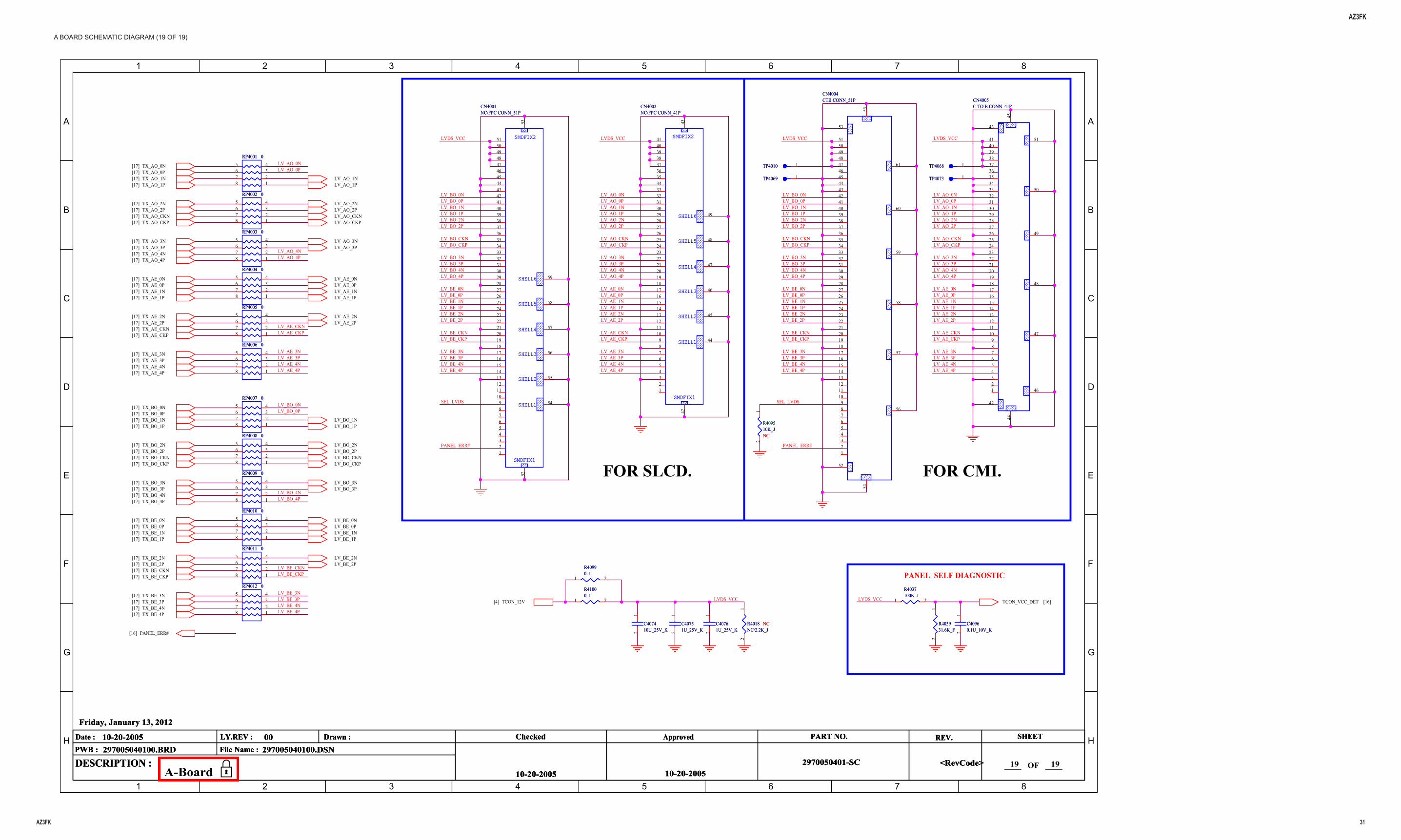
AZ3FK 31
AZ3FK
A BOARD SCHEMATIC DIAGRAM (19 OF 19)
1
1
2
2
3
3
4
4
5
5
6
6
7
7
8
8
A A
B B
C C
D D
E E
F F
G G
H H
LV_AO_0NLV_AO_0P
LV_AO_4NLV_AO_4P
LV_AE_CKNLV_AE_CKP
LV_AE_3NLV_AE_3PLV_AE_4NLV_AE_4P
LV_BO_0NLV_BO_0P
LV_BO_4NLV_BO_4P
LV_BE_CKNLV_BE_CKP
LV_BE_3NLV_BE_3PLV_BE_4NLV_BE_4P
LVDS_VCC LVDS_VCC
LV_BO_0NLV_BO_0PLV_BO_1NLV_BO_1PLV_BO_2NLV_BO_2P
LV_BO_CKNLV_BO_CKP
LV_BO_3NLV_BO_3PLV_BO_4NLV_BO_4P
LV_BE_0NLV_BE_0PLV_BE_1NLV_BE_1PLV_BE_2NLV_BE_2P
LV_BE_CKNLV_BE_CKP
LV_BE_3NLV_BE_3PLV_BE_4NLV_BE_4P
LV_AO_0NLV_AO_0PLV_AO_1NLV_AO_1PLV_AO_2NLV_AO_2P
LV_AO_CKNLV_AO_CKP
LV_AO_3NLV_AO_3PLV_AO_4NLV_AO_4P
LV_AE_0NLV_AE_0PLV_AE_1NLV_AE_1PLV_AE_2NLV_AE_2P
LV_AE_CKNLV_AE_CKP
LV_AE_3NLV_AE_3PLV_AE_4NLV_AE_4P
LV_AO_0NLV_AO_0PLV_AO_1NLV_AO_1PLV_AO_2NLV_AO_2P
LV_AO_CKNLV_AO_CKP
LV_AO_3NLV_AO_3PLV_AO_4NLV_AO_4P
LV_AE_0NLV_AE_0PLV_AE_1NLV_AE_1PLV_AE_2NLV_AE_2P
LV_AE_CKNLV_AE_CKP
LV_AE_3NLV_AE_3PLV_AE_4NLV_AE_4P
LV_BO_0NLV_BO_0PLV_BO_1NLV_BO_1PLV_BO_2NLV_BO_2P
LV_BO_CKNLV_BO_CKP
LV_BO_3NLV_BO_3PLV_BO_4NLV_BO_4P
LV_BE_0NLV_BE_0PLV_BE_1NLV_BE_1PLV_BE_2NLV_BE_2P
LV_BE_CKNLV_BE_CKP
LV_BE_3NLV_BE_3PLV_BE_4NLV_BE_4P
LVDS_VCC
SEL_LVDS
LVDS_VCC
PANEL_ERR# PANEL_ERR#
SEL_LVDS
LVDS_VCCLVDS_VCC
TX_AO_0N[17]TX_AO_0P[17]TX_AO_1N[17]TX_AO_1P[17]
TX_AO_2N[17]TX_AO_2P[17]TX_AO_CKN[17]TX_AO_CKP[17]
TX_AO_3N[17]TX_AO_3P[17]TX_AO_4N[17]TX_AO_4P[17]
TX_AE_0N[17]TX_AE_0P[17]TX_AE_1N[17]TX_AE_1P[17]
TX_AE_2N[17]TX_AE_2P[17]TX_AE_CKN[17]TX_AE_CKP[17]
TX_AE_3N[17]TX_AE_3P[17]TX_AE_4N[17]TX_AE_4P[17]
LV_AO_1NLV_AO_1P
LV_AO_CKNLV_AO_CKP
LV_AO_2NLV_AO_2P
LV_AO_3NLV_AO_3P
LV_AE_1NLV_AE_1P
LV_AE_0NLV_AE_0P
LV_AE_2NLV_AE_2P
LV_BO_1NLV_BO_1P
LV_BO_CKNLV_BO_CKP
LV_BO_2NLV_BO_2P
LV_BO_3NLV_BO_3P
LV_BE_1NLV_BE_1P
LV_BE_0NLV_BE_0P
LV_BE_2NLV_BE_2P
TX_BO_0N[17]TX_BO_0P[17]TX_BO_1N[17]TX_BO_1P[17]
TX_BO_2N[17]TX_BO_2P[17]TX_BO_CKN[17]TX_BO_CKP[17]
TX_BO_3N[17]TX_BO_3P[17]TX_BO_4N[17]TX_BO_4P[17]
TX_BE_0N[17]TX_BE_0P[17]TX_BE_1N[17]TX_BE_1P[17]
TX_BE_2N[17]TX_BE_2P[17]TX_BE_CKN[17]TX_BE_CKP[17]
TX_BE_3N[17]TX_BE_3P[17]TX_BE_4N[17]TX_BE_4P[17]
PANEL_ERR#[16]
TCON_VCC_DET [16]TCON_12V[4]
Drawn : Checked ApprovedFile Name :
PART NO.Date : LY.REV : REV. SHEET
____ OF ____
PWB :
DESCRIPTION : 19<RevCode>
10-20-2005297005040100.BRD
00297005040100.DSN
10-20-2005 10-20-20052970050401-SC 19
Friday, January 13, 2012
Drawn : Checked ApprovedFile Name :
PART NO.Date : LY.REV : REV. SHEET
PWB :
DESCRIPTION : <RevCode>
10-20-2005297005040100.BRD
00297005040100.DSN
10-20-2005 10-20-20052970050401-SC
Friday, January 13, 2012
Drawn : Checked ApprovedFile Name :
PART NO.Date : LY.REV : REV. SHEET
PWB :
DESCRIPTION : <RevCode>
10-20-2005297005040100.BRD
00297005040100.DSN
10-20-2005 10-20-20052970050401-SC
Friday, January 13, 2012
.IMC ROF.DCLS ROF
PANEL SELF DIAGNOSTIC
RP4011 0RP4011 0
12345
678
CN4004CTB CONN_51PCN4004CTB CONN_51P
4140393837363534333231302928272625242322212019181716151413121110987654321
42434445464748495051
52
53
5455
56
57
58
59
60
61RP4001 0RP4001 0
12345
678
CN4005C TO B CONN_41PCN4005C TO B CONN_41P
43
42
4445
46
47
48
49
50
514140393837363534333231302928272625242322212019181716151413121110987654321
RP4009 0RP4009 0
12345
678
TP4073TP4073 1
RP4005 0RP4005 0
12345
678
TP4010TP4010 1
C40751U_25V_KC40751U_25V_K
12
R4018NC/2.2K_J
NCR4018NC/2.2K_J
NC
12
RP4002 0RP4002 0
12345
678
C40761U_25V_KC40761U_25V_K
12
R41000_JR41000_J
1 2
RP4003 0RP4003 0
12345
678
R403931.6K_FR403931.6K_F
12
RP4007 0RP4007 0
12345
678
RP4012 0RP4012 0
12345
678
TP4069TP4069 1
SMDFIX1
SMDFIX2
SHELL1
SHELL2
SHELL3
SHELL4
SHELL5
SHELL6
CN4002NC/FPC CONN_41P
SMDFIX1
SMDFIX2
SHELL1
SHELL2
SHELL3
SHELL4
SHELL5
SHELL6
CN4002NC/FPC CONN_41P
10987654321
41
42
20191817161514131211
39383736353433323130292827262524232221
40
43
44
45
46
47
48
49
RP4006 0RP4006 0
12345
678
RP4010 0RP4010 0
12345
678
R4037100K_JR4037100K_J
1 2
SMDFIX1
SMDFIX2
SHELL1
SHELL2
SHELL3
SHELL4
SHELL5
SHELL6
CN4001NC/FPC CONN_51P
SMDFIX1
SMDFIX2
SHELL1
SHELL2
SHELL3
SHELL4
SHELL5
SHELL6
CN4001NC/FPC CONN_51P
10987654321
4142
20191817161514131211
39383736353433323130292827262524232221
40
434445464748495051
5253
54
55
56
57
58
59
R409510K_JNC
R409510K_JNC
12
RP4008 0RP4008 0
12345
678
C407410U_25V_KC407410U_25V_K
12
RP4004 0RP4004 0
12345
678
R40990_JR40990_J
1 2
C40960.1U_10V_KC40960.1U_10V_K
12
TP4068TP4068 1
A-Board

AZ3FK 32
AZ3FK
1 | 2 | 3 | 4 | 5 | 6 | 7 | 8 | 9 | 10 | 11 | 12 | 13 | 14 | 15 | 16 | 17 | 18 | 19 | 20 | 21 | 22 | 23 | 24 | 25 | 26 | 27 | 28 |
A
—
B
—
C
—
D
—
E
—
F
—
G
—
H
—
I
—
J
—
K
—
L
—
M
—
N
—
O
—
P
—
A [POWER STRUCTURE/POWER DISTRIBUTION/VGA/YPBPR AND AV/HDMI/RF TUNER/DDR/FRONT END/ETHERNET/USB/FLASH/RX-TX/CI AND SUB-BD/AUDIO AMP/LINE OUT/SPDIF/LVDS]COMPONENT SIDE
KDL-40/46/55EX640 ONLY
1 | 2 | 3 | 4 | 5 | 6 | 7 | 8 | 9 | 10 | 11 | 12 | 13 | 14 | 15 | 16 | 17 | 18 | 19 | 20 | 21 | 22 | 23 | 24 | 25 | 26 | 27 | 28 |
A
—
B
—
C
—
D
—
E
—
F
—
G
—
H
—
I
—
J
—
K
—
L
—
M
—
N
—
O
—
P
—
ACONDUCTOR SIDE[POWER STRUCTURE/POWER DISTRIBUTION/VGA/YPBPR AND AV/HDMI/RF TUNER/DDR/FRONT END/ETHERNET/USB/FLASH/RX-TX/CI AND SUB-BD/AUDIO AMP/LINE OUT/SPDIF/LVDS]

AZ3FK
AZ3FK 33
G9 BOARD SCHEMATICREFER TO “SECTION 2: ELECTRICAL PARTS LIST” ON PAGE 41 TO DETERMINE IF THIS BOARD IS USED IN THE MODEL BEING REPAIRED
G9 BOARD SCHEMATIC AND PCB NOT AVAILABLE1 | 2 | 3 | 4 | 5 | 6 | 7 | 8 | 9 | 10 |
A
—
B
—
C
—
D
—
E
—
F
—
G
—

AZ3FK
AZ3FK 34
G10 BOARD SCHEMATICREFER TO “SECTION 2: ELECTRICAL PARTS LIST” ON PAGE 41 TO DETERMINE IF THIS BOARD IS USED IN THE MODEL BEING REPAIRED
G10 BOARD SCHEMATIC AND PCB NOT AVAILABLE1 | 2 | 3 | 4 | 5 | 6 | 7 | 8 | 9 | 10 |
A
—
B
—
C
—
D
—
E
—
F
—
G
—

AZ3FK
AZ3FK 35
G11 BOARD SCHEMATICREFER TO “SECTION 2: ELECTRICAL PARTS LIST” ON PAGE 41 TO DETERMINE IF THIS BOARD IS USED IN THE MODEL BEING REPAIRED
G11 BOARD SCHEMATIC AND PCB NOT AVAILABLE1 | 2 | 3 | 4 | 5 | 6 | 7 | 8 | 9 | 10 |
A
—
B
—
C
—
D
—
E
—
F
—
G
—

AZ3FK
AZ3FK 36
GE55 BOARD SCHEMATICREFER TO “SECTION 2: ELECTRICAL PARTS LIST” ON PAGE 41 TO DETERMINE IF THIS BOARD IS USED IN THE MODEL BEING REPAIRED
GE55 BOARD SCHEMATIC AND PCB NOT AVAILABLE1 | 2 | 3 | 4 | 5 | 6 | 7 | 8 | 9 | 10 |
A
—
B
—
C
—
D
—
E
—
F
—
G
—

AZ3FK
AZ3FK 37
GL5A BOARD SCHEMATICREFER TO “SECTION 2: ELECTRICAL PARTS LIST” ON PAGE 41 TO DETERMINE IF THIS BOARD IS USED IN THE MODEL BEING REPAIRED
GL5A BOARD SCHEMATIC AND PCB NOT AVAILABLE1 | 2 | 3 | 4 | 5 | 6 | 7 | 8 | 9 | 10 |
A
—
B
—
C
—
D
—
E
—
F
—
G
—

AZ3FK
AZ3FK 38
GL5B BOARD SCHEMATICREFER TO “SECTION 2: ELECTRICAL PARTS LIST” ON PAGE 41 TO DETERMINE IF THIS BOARD IS USED IN THE MODEL BEING REPAIRED
GL5B BOARD SCHEMATIC AND PCB NOT AVAILABLE1 | 2 | 3 | 4 | 5 | 6 | 7 | 8 | 9 | 10 |
A
—
B
—
C
—
D
—
E
—
F
—
G
—

AZ3FK
AZ3FK 39
H BOARD SCHEMATIC
1 | 2 | 3 | 4 | 5 | 6 | 7 | 8 | 9 | 10 |
A
—
B
—
C
—
D
—
E
—
F
—
G
—
GND_1
GND_1
XXC103
1
2
3
4
5
6
7
7PCN100
STBY+3.3V
LED_POWER
GND
LED_STBY
LED_TIMER
LED_PIC_MUTE
SIRCS
Q100XX
Q101XX
Q102XX
Q103XX
GND_1
D104XX
D105XX
D106XX D107
XX
XXC100
R102XX
R104XX
XXC102
XXC101
D108XX
1608
10V1
X7R
C104
1/10WRN-CP
R112
5%
100
1/10WRN-CP
100R113
5%
XXR106 R111
XX
R101
5%RN-CP1/10W
2201/10WRN-CP
5%
R105820
1/10WRN-CP
5%
1kR107
1/10WRN-CP
5%
R110220
R100
CHIP0
R103
CHIP0
R108
CHIP0
R109
CHIP0
Vs
Vou
t
GN
D1
GN
D2
RS-970*IC100
SML-D13M8WT86S*D100 *D101
SML-D12Y8WT86SP SML-D12U8WT86*D102 *D103
SML-D13M8WT86S
D101:TIMER(AMBER) D103:POWER(GREEN)
Use compatible macro pattern with GOODTAKE
High: LED onLow : LED off
LED
D100:PICTURE OFF(GREEN)
Macro code=UPB472CRA
S i rcs
D102:STANDBY(RED)

AZ3FK
AZ3FK 40
H1 | 2 | 3 | 4 | 5 | 6 | 7 | 8 | 9 | 10 | 11 | 12 | 13 | 14 | 15 | 16 | 17 | 18 | 19 | 20 | 21 | 22 | 23 | 24 | 25 | 26 | 27 | 28 |
A
—
B
—
C
—
D
—
E
—
F
—
G
—
H
—
I
—
J
—
K
—
L
—
M
—
N
—
O
—
P
—
[LED/SIRCS]
[LED/SIRCS]
COMPONENT SIDE
CONDUCTOR SIDEH
1 | 2 | 3 | 4 | 5 | 6 | 7 | 8 | 9 | 10 | 11 | 12 | 13 | 14 | 15 | 16 | 17 | 18 | 19 | 20 | 21 | 22 | 23 | 24 | 25 | 26 | 27 | 28 |
A
—
B
—
C
—
D
—
E
—
F
—
G
—
H
—
I
—
J
—
K
—
L
—
M
—
N
—
O
—
P
—
( 1 - 7 3 3 - 1 7 7 - 1 1 )
1 - 8 8 5 - 5 8 4 - 1 1 R1S T B Y
IC100
C N 1 0 0
I RP - O F F
P W RT M Rcam10
cam13
cam14
cam15cam16
cam20 cam21
cam22
cam24cam25
cam26
cam28cam9
( 1 - 7 3 3 - 1 7 7 - 1 1 )1 - 8 8 5 - 5 8 4 - 1 1
R 1
MD E P G W L Pcam10
cam13
cam14
cam15 cam16
cam20cam21
cam22
cam24cam25
cam26
cam28 cam9

AZ3FK 41
AZ3FK
REF. NO. PART NO. DESCRIPTION VALUES
When ordering parts by referencenumber, please include the board name.
REF. NO. PART NO. DESCRIPTION VALUES
NOTE: The components identified by shading and ! mark are critical for safety. Replace only with part number specified.
NOTE: The components identified by a red outline and a mark contain confidential information. Specific instructions must be adhered to whenever these components are repaired and/or replaced. See Appendix A: Encryption Key Components in the back of this manual.
AFTER REPLACING THE MAIN BOARD OR LCD PANEL YOU MUST UPDATE THE SOFTWARE TO THE LATEST VERSION AND COMPLETE ANY SERVICE ADJUSTMENTS
* Items marked with an asterisk are not stocked since they are seldom required for routine service. Expect some delay when ordering these components.
RESISTORS• All resistors are in ohms• F : nonflammable• All variable and adjustable resistors have
characteristic curve B, unless otherwise noted.NOTE: Les composants identifies per un trame et une marque ! sont critiques pour la securite. Ne les remplacer que par une piece portant le numero specifie.
SECTION 2: ELECTRICAL PARTS LIST
G11 1-474-382-12 G11 BOARD COMPLETE (KDL-46BX450 ONLY)
H 1-895-183-11 H BOARD, MOUNTED
KDL-40BX451/46BX451
A 1-895-182-31 A BOARD, COMPLETE
G10 1-474-380-11 G10 BOARD, COMPLETE (KDL-40BX450 ONLY)
G11 1-474-382-12 G11 BOARD COMPLETE (KDL-46BX451 ONLY)
H 1-895-183-11 H BOARD, MOUNTED
KDL-40BX453/46BX453
A 1-895-182-61 A BOARD, COMPLETE
G10 1-474-380-11 G10 BOARD, COMPLETE (KDL-40BX453 ONLY)
G11 1-474-380-12 G11 BOARD, COMPLETE (KDL-46BX453 ONLY)
H 1-895-183-11 H BOARD, MOUNTED
KDL-32BX353/32BX354
A 1-895-182-41 A BOARD, COMPLETE (KDL-32BX353 ONLY) 1-895-182-51 A BOARD, COMPLETE (KDL-32BX354 ONLY)
G9 1-474-381-12 G9 BOARD, COMPLETE
H 1-895-183-11 H BOARD, MOUNTED
KDL-32BX355/32BX356
A 1-895-184-21 A BOARD, COMPLETE (KDL-32BX355 ONLY) 1-895-184-31 A BOARD, COMPLETE (KDL-32BX356 ONLY)
G9 1-474-381-12 G9 BOARD, COMPLETE
H 1-895-183-11 H BOARD, MOUNTED
KDL-40BX450/46BX450
A 1-895-182-11 A BOARD, COMPLETE (FOR CND/MX/US MODELS ONLY) 1-895-182-21 A BOARD, COMPLETE (FOR LA MODELS ONLY)
G10 1-474-380-11 G10 BOARD, COMPLETE (KDL-40BX450 ONLY)

AZ3FK 42
AZ3FK
REF. NO. PART NO. DESCRIPTION VALUES REF. NO. PART NO. DESCRIPTION VALUES
AFTER REPLACING THE MAIN BOARD OR LCD PANEL YOU MUST UPDATE THE SOFTWARE TO THE LATEST VERSION AND COMPLETE ANY SERVICE ADJUSTMENTS
KDL-40BX455/46BX455
A 1-895-184-11 A BOARD, COMPLETE
G10 1-474-380-11 G10 BOARD, COMPLETE (KDL-40BX455 ONLY)
G11 1-474-380-12 G11 BOARD, COMPLETE (KDL-46BX455 ONLY)
H 1-895-183-11 H BOARD, MOUNTED
KDL-40EX640/46EX640/55EX640
A 1-895-172-11 A BOARD, COMPLETE
GL5 1-895-173-11 GL5A BOARD, COMPLETE (KDL-40EX640 ONLY) 1-895-174-11 GL5B BOARD COMPLETE (KDL-46EX640 ONLY)
GE55 1-895-175-11 GE55 BOARD, COMPLETE (KDL-55EX640 ONLY)
H 1-895-176-11 H BOARD, MOUNTED
ACCESSORIES AND PACKING FOR US ONLY
4-408-075-31 BAG, PROTECTION (1400x900) (KDL-40BX450/40EX640 ONLY) 4-408-076-31 BAG, PROTECTION (1550x1050) (KDL-46BX450/46EX640 ONLY) 4-408-077-31 BAG,PROTECTION (1720X1200) (KDL-55EX640 ONLY)
4-416-841-01 CARTON, INDIVIDUAL (APO 40) (KDL-40BX450 ONLY) 4-416-845-01 CARTON, INDIVIDUAL (APO 46) (KDL-46BX450 ONLY) 4-419-122-01 CARTON, INDIVIDUAL (NK2 40) (KDL-40EX640 ONLY) 4-419-123-01 CARTON, INDIVIDUAL (NK2 46) (KDL-46EX640 ONLY)
4-423-892-01 CUSHION, LOWER (40APOF) (KDL-40BX450 ONLY) 4-400-053-11 CUSHION, LOWER (40 ZEU) (KDL-40EX640 ONLY) 4-423-894-01 CUSHION, LOWER (46APOF) (KDL-46BX450 ONLY) 4-400-054-11 CUSHION, LOWER (46 ZEU) (KDL-46EX640 ONLY) 4-400-055-12 CUSHION, LOWER (55 ZEU) (KDL-55EX640 ONLY)
4-412-149-11 CUSHION, SIDE CENTER L (55 ZEU) (KDL-55EX640 ONLY) 4-412-150-11 CUSHION, SIDE CENTER R (55 ZEU) (KDL-55EX640 ONLY)
4-423-891-01 CUSHION, UPPER (40APOF) (KDL-40BX450 ONLY) 4-400-047-11 CUSHION, UPPER (40 ZEU) (KDL-40EX640 ONLY) 4-423-893-01 CUSHION, UPPER (46APOF) (KDL-46BX450 ONLY) 4-400-048-11 CUSHION, UPPER (46 ZEU) (KDL-46EX640 ONLY) 4-400-049-11 CUSHION, UPPER (55 ZEU) (KDL-55EX640 ONLY)
4-419-434-11 LABEL, ENERGY GUIDE(APO) (KDL-40BX450 ONLY) 4-420-093-01 LABEL, ENERGY GUIDE(NK2) (KDL-40EX640 ONLY) 4-419-434-21 LABEL, ENERGY GUIDE(APO) (KDL-46BX450 ONLY) 4-420-093-11 LABEL, ENERGY GUIDE(NK2) (KDL-46EX640 ONLY) 4-420-093-21 LABEL, ENERGY GUIDE(NK2) (KDL-55EX640 ONLY)
4-419-125-01 LABEL, FRONT (NK2 40) (KDL-40EX640 ONLY) 4-419-126-01 LABEL, FRONT (NK2 46) (KDL-46EX640 ONLY) 4-419-127-01 LABEL, FRONT (NK2 55) (KDL-55EX640 ONLY)
3-674-673-22 STOPPER (A) (KDL-55EX640 ONLY)
4-400-062-11 TRAY (55 ZEU) (KDL-55EX640 ONLY)

AZ3FK
Sony CorporationSony Technology Center
Technical ServicesService Publication Department9-883-884-53
English2012BJ74WEB-1
Printed in USA© 2012.2
is a trademark of Sony Electronics
Reproduction in whole or part without written permission is prohibited. All rights reserved
AZ3FK A-1
APPENDIX A: ENCRYPTION KEY COMPONENTS
Encryption key components developed by Sony Corporation contain confidential information, and shall be handled under the non-disclosure obligations provided in the applicable agreement with Sony Corporation (and/or its subsidiary).
As part of this agreement specific instructions must be adhered to whenever a Circuit Board containing encryption key components is repaired and/or replaced pursuant to the following:
1. In the service manual the Circuit Board(s. containing encryption key components shall be identified with a red outline and a .
2. Only repair boards or components listed in the service manual shall be utilized for replacement and/or repair.
3. Disassembly, decryption, or reverse-engineering component(s. is strictly prohibited.
4. Any board in which the Servicer replaces an encryption key component must be placed back into the set it orignally came from and the replaced defective component MUST BE DESTROYED. Boards cannot be swapped.
5. If a Circuit Board identified with a red outline and a in the service manual is deemed to be defective:
a. and if a core charge is imposed and is covered under the product warranty, the defective un-repaired or modified board MUST BE RETURNED to Sony.
b. and if the core charge is NOT covered under the product warranty, the defective un-repaired or modified board MUST BE DESTROYED.
6. If a unit is destroyed (such as field scrap., the Circuit Board identified with a red outline and a in the service manual MUST BE DESTROYED.