shaping amplifier - iuac
TRANSCRIPT

TECHNICAL REPORT
TITLE :Technical Report on Spectroscopy Amplifier
AUTHORS : S.Venkataramanan, Arti Gupta
CATEGORY : Instrumentation
REFERENCE NO : NSC/TR/SV/2002-03/29
NUCLEAR SCIENCE CENTRE(An Autonomous Inter-University Centre of UGC)
Post Box No.: 10502, Aruna Asaf Ali Marg,New Delhi 110067 (India) Phone: 2689 3955, 2689 2603, 2689 2601
Fax: 091-11-2689 3666 Email: [email protected]

TECHNICAL REPORT
ON SPECTROSCOPY AMPLIFIER
CONTENTS
1. Abstract
2. Acknowledgment
3. Specifications
4. Introduction
5. Principle of operations
6. Pile Up rejection
7. Performances
8. Assembly Procedure
9. References
10.Schematic, Block and signal level diagrams
11.Bill of material
12.PCB artwork TOP, BOTTOM layers
13.Silk screen TOP, BOTTOM layers
14.Drill drawing
Prepared by
ELECTRONICS LABORATORY
NUCLEAR SCIENCE CENTRE,
P.B.10502,
NEW DELHI 110067.

Technical Report on
Spectroscopy AmplifierS.Venkataramanan*, Arti Gupta
Electronics Laboratory, Nuclear Science Centre, P.B.10502, Aruna Asaf Ali Marg,
New Delhi 110067.*email: [email protected]
AbstractAs a part of on going nuclear electronics development activities for INGA
project at NSC, we have successfully developed a high density Spectroscopy amplifier
for Clover detector with SMD technology. It essentially consists of active Pole-Zero
(P/Z) compensation, gain stages, active shaping, Gated BLR correction, Pileup
Rejection (PUR) logic and buffer circuits. It has the options for remote P/Z adjustment
and threshold setting for base line restorer (BLR) correction.
Various prototypes have been tested with Clover detectors. In this report the
principle of operation of various circuit blocks are explained along with representative
test point signals. Assembly and troubleshooting procedures are given. The amplifier
specifications and test results are given and possible improvements are also suggested.
Acknowledgment
We would like to thank engineers from GIP, Ganil, France for their constant
support in simulating various circuit blocks and fruitful discussions. We also would like
to thank INGA project group at NSC for specifying and evaluating spectroscopy
amplifiers and providing funds for development. At last, our sincere thanks to Prof.
G.K.Mehta, Dr.Amit Roy and Ajith Kumar.B.P, for their constant encouragement and
providing the necessary infrastructure inorder to complete this project successfully.
Introduction

A nuclear spectroscopy (shaping) amplifier is a signal amplifier with complete
DC correction control loop, while shaping the nuclear detector pulses of short rise time
and long fall time into a finite width semi-Gaussian shape, which can be digitized with
ADC. A typical modern shaping amplifier consists of a P/Z correction, gain stages,
active integration, Active gated base line restorer and coaxial cable driver while
providing convenient synchronous (BUSY) and pile up reject (PUR) logic pulses.
We have incorporated all above features in our shaping amplifier, in which the
shaping time constant is fixed. The Pole-Zero adjustment and manual threshold settings
can be done from either front panel or thorough remotely controlled digital to analog
converter(DAC). Three gain selections are possible with onboard jumper selection. In
order to reduce dead time related to overload, we have incorporated limiters in gain
stages for fast recovery. The Quasigaussian pulse shaping is achieved with early passive
differentiation stage and 2 stages of second order active integration. Slow base line shift
due to power line pickup or offset errors due to operational amplifier are corrected with
sophisticated gated base line restorer. The piled up events, which would cause poor
energy resolution can be rejected with PUR logic pulse at ADC level. A 50 ohm coaxial
buffer amplifier is wired in a composite amplifier configuration in order to achieve good
high frequency and DC responses.
The entire amplifier is wired as a daughter card on a double sided glass epoxy
PCB with surface mount components to achieve required high density.

Principle of OperationThe shaping amplifier schematic is divided into Analog and digital sections and
a block diagram is also attached for quick reference. The nuclear radiation pulses
received from HPGe which have nominal amplitude of -200mV/MeV and decay time of
50µS(±5%). The early differentiation is done with passive RC components for 3µS
(C3,C4,R13). The Coarse Pole-Zero(P/Z) correction is done with (R19, C3,C4) and fine
adjustment with in ±5% can be done from front panel potentiometer (R14) when remote
control is not desired. The remote P/Z adjustment is implemented with wide bandwidth
Analog multiplier, which replaces potentiometer. It can also accept control voltage
(P/Z_adj.) from remote DAC. The multiplier output can also be used for P/Z
compensation in timing channel (TFA).
The differentiated pulse is amplified with low noise high quality operational
amplifier (U2). The feedback resistor is varied (jumper selected) for different gain
settings (2MeV, 4MeV, 6MeV) as per the user requirement. The pulse is further
amplified with low noise operational amplifier (U1). These two stages are wired with
clamping circuit in feedback path to speedup overload recovery. The amplified pulses
are shaped with 2 stages of 2nd order active integration (U3 A&B), where RC
components are chosen for required shaping time constant 3µS, to provide smooth
quasigaussian shaped pulses. While amplifying the signals in previous stages, any
offset or DC shift voltages generated are to be corrected for obtaining correct energy
information. This is achieved with sophisticated gated base line restorer (U6A&B, U7,
C19, Q1) which is essentially a closed control loop, with active integration in its
feedback path to provide overall differentiation action.
Since the BLR correction cannot be done during presence of pulses, the
integrator is gated with elaborate gating circuit (U8 to U11) and level converter. The
gate for BLR is generated from Look ahead command, which indicates the presence of
energy signal and Wrap around command, which indicates the end of energy pulse.

The look ahead command is generated in U9A, which is an ultra fast comparator
(TTL) which compares, the differentiated (300nS) BLR corrected input pulse (BG_IN)
and external BLR threshold (U8), which is usually set above input noise level. The
presence of energy pulse is indicated by activating a monoshot (U10). The Wrap around
command is generated by comparing (U9B) BLR threshold and V_SHAPE, the shaped
output pulse, to indicate the end of energy pulse, where the BLR threshold is set just
above output noise level. These two commands are processed (U11) to generate a
BLR_CONT control command, which would switch the transconductance amplifier
(U7) accordingly in BLR control loop. The "BUSY" logic pulse essentially indicates
the presence of energy pulse, which is often used to synchronize the ADC.
Pile-Up Rejection
In a HPGe detector, when two gamma rays arrive within the width of the shaping
amplifier output pulse, the respective amplifier pulses pileup and generate a distorted
pulse and cause poor energy resolution. In such cases, where charge collection time is
shorter than peaking time of the amplifier, a PUR pulse can be used to reject such pulses
from being processed further.
In this amplifier, the presence of energy signal is indicated by Look ahead
command, CLK, in turn a 20µS width pulse is generated which is inspection interval
for PUR. The associated D flip-flop, would output pulse having width of inspection
interval as PUR logic pulse, upon receiving another Look ahead command within the
inspection interval.

Assembly Procedure
The currently (PT-5_CORR) available PCB is of glass epoxy, double sided with
0.7mm drill PTH having dimension of 4" x 1.75" with all above features. This has
additional provision of PUR logic output. All developed prototypes have common PCB
foot prints in order to use them conveniently.
It is recommended to have solder mask and silk screen printed on both sides for
easy assembly as well to protect it from solder bridges etc.,. Use of 0.8mm sharp solder
tip, IC solder tips are recommended in order to solder narrowly spaced SMT devices.
SMT devices shall be picked only by fine quality tweezers. While soldering a magnifier
x5 (large) and x12 (eye piece) is used to assure the soldering. It is essential to use solder
cleaning liquid with cotton swab to remove dust attracting solder paste.
The PCB shall be checked with magnifiers and multimeter for any unwanted
connections and PTHs. Then components shall be soldered in a orderly manner, to start
with all low profile chip resistors and capacitors. It is essential to check the impedance
between various nodes after soldering resistors, capacitors and inductors. Active
components like diodes, transistors and ICS are soldered thereafter. At last tantalum
capacitors, connectors, jumpers and any non-SMT devices. All PCBs shall be marked
distinctly with unique number for any future references.
ReferencesThe following references were proven to be very useful to design and test our
shaper.
1. Radiation detection systems, Lecture notes on Pulse Processing techniques in
radiation & spectrometry, S.K.Kataria, BARC.
2. EG&G ORTEC catalogue
3. Opamps for Everyone, Ron Moncini, M/s. TI, USA (SL0D006A)
4. Design with OPAMPS and Analog Integrated Circuits, Sergio Franco, McGraw-
Hill
5.Techniques for Nuclear & Particle physics Experiments, W.R.Leo, Springer Verlog
6. Radiation Detectors Physical Principles & Applications, Delaney, Finch,
Clardrendon Press
7. Spectroscopy Amplifier, Instruction manual, M/s. SILENA, Italy.
8. Signal processing for semi-conductor detectors, F.S.Goulding, A.Landis, IEEE
Transact. NS-29, Vol:3, June 1982.

SPECIFICATIONS: SPECTROSCOPY AMPLIFIER
Input Impedance ~1000 ohmPole/Zero adj. Input pulse having decay time about 50µSec (±5%)
can be corrected through potentiometer (FP) or remote controlled through DAC. Zin: 1Kohm.Control voltage not to exceed ± 1Volt.
Shaping time & type ~3 µSec. Fixed, Active integration (4th order)Quasi Gaussian having peaking time of ~2.4τs.
Input signal* -200mV/MeV is expected to generate +10Volts at the output for 3 gain settings. Not to exceed ±5V.
Gain 2MeV, 4MeV and 6 MeV for +10V output. Jumper selection on board. Default is 2 MeV.
BLR threshold Manual baseline restorer threshold is set through Potentiometer (FP) or remotely. Range is 0 to 500mV when provided. Zin: 1k. Control voltage not to exceed ±5V.
Output Unipolar, Gated BLR DC restored. Width :~20µSec. Zo: 50 ohms.
BUSY A TTL negative logic pulse for the duration of presence of output pulse exceeds BLR threshold.Zo: 10 ohms
PUR Pile up reject signal is a TTL logic signal, with pileup inspection interval of 20µSec. Zo: 10 ohms
Power required +/-6V, 40mA/20mA+/-12V 40mA/30mA+24V 5mA
Size & Weight W x H x L : 1.75"x0.5"x 4", 30 grams.
PERFORMANCES:
The module has been subjected to various tests at NSC with 60Co and 152Eu sources and in beam, in parallel with commercial modules with 8K MCA. The typical results obtained are :
Resolution: 1.3KeV (122KeV), 2.0 KeV (1408 KeV) of 60Co @ 9 Kcps.Integral non-linearity: ± 100 eV for 152Eu spectrum, 2MeV/~8V. Stability: With 60Co, no significant shift observed at 6 kcps in 55 hours.

Fig: Photo of Shaper Daughter Card
Fig: Typical BUSY, P/Z Monitor Signals of a Ge. Detector.

Gain Selection Procedure:
The Shaper is designed to work with one of the three different GAIN settings
2MeV*/4MeV/6MeV as per user requirement. The GAIN can be selected on the
SHAPER daughter card by the procedure given here.
1. Open the side panel of Clover Electronics Module
2. Locate the SHAPERS in TOP of Mother Board.
3. Identify JUMPER SOCKETS in extreme right corner facing top. (Ref. Photograph)
4. By plugging 'in' any on the jumper will select 4MeV.
5. By plugging 'in' both jumpers will select 6MeV.
* Default GAIN selection when jumpers not used.
Pole_Zero Adjustment:
The Shaper is designed to work with Eurisys Measures Clover detectors with
preamplifiers having 50µS (±10%) decay time constant. The Pole_Zero adjustment can
be done with front panel PZ_Adj. Potentiometer while monitoring corresponding front
panel PZ_ Mon. on a CRO.
BLR Adjustment:
The Shaper is designed to have stable zero reference at all specified working
conditions. This is achieved by Gated BLR operation. The required threshold level
above system noise is fed through front panel BLR adj. potentiometer. This is set while
monitoring front panel BUSY (TTL) signal on a CRO for a minimum count rate when
no radiation sources are used. It is essential to set proper Pole Zero adjustment for
proper functioning of BLR.
During above procedures, it is recommanded to use BUSY signal to trigger CRO.
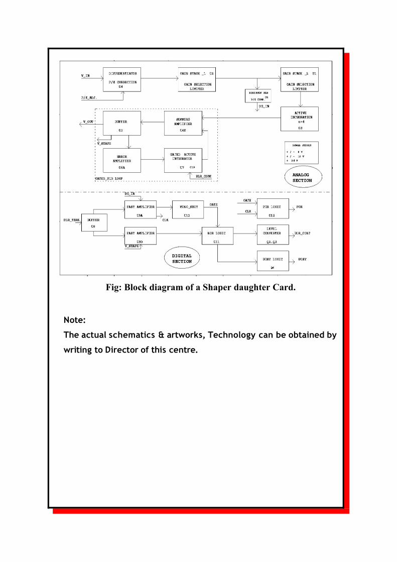
Fig: Block diagram of a Shaper daughter Card.
Note:
The actual schematics & artworks, Technology can be obtained by
writing to Director of this centre.