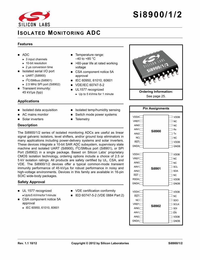
si8900/1/2 - silicon labs · pdf filepin assignments vddb nc nc scl sda nc vddb gndb si8901...
TRANSCRIPT
Rev. 1.1 10/12 Copyright © 2012 by Silicon Laboratories Si8900/1/2
Si8900/1/2
ISOLATED MONITORING ADC
Features
Applications
Description
The Si8900/1/2 series of isolated monitoring ADCs are useful as linearsignal galvanic isolators, level shifters, and/or ground loop eliminators inmany applications including power-delivery systems and solar inverters.These devices integrate a 10-bit SAR ADC subsystem, supervisory statemachine and isolated UART (Si8900), I2C/SMbus port (Si8901), or SPIPort (Si8902) in a single package. Based on Silicon Labs’ proprietaryCMOS isolation technology, ordering options include a choice of 2.5 or5 kV isolation ratings. All products are safety certified by UL, CSA, andVDE. The Si8900/1/2 devices offer a typical common-mode transientimmunity performance of 45 kV/µs for robust performance in noisy andhigh-voltage environments. Devices in this family are available in 16-pinSOIC wide-body packages.
Safety Approval
ADC3 input channels10-bit resolution2 µs conversion time
Isolated serial I/O portUART (Si8900)I2C/SMbus (Si8901)2.5 MHz SPI port (Si8902)
Transient immunity:45 kV/µs (typ)
Temperature range:–40 to +85 °C
>60-year life at rated working voltage
CSA component notice 5A approval
IEC 60950, 61010, 60601 VDE/IEC 60747-5-2 UL1577 recognized
Up to 5 kVrms for 1 minute
Isolated data acquisition AC mains monitor Solar inverters
Isolated temp/humidity sensing Switch mode power systems Telemetry
UL 1577 recognizedUp to 5 kVrms for 1 minute
CSA component notice 5A approvalIEC 60950, 61010, 60601
VDE certification conformity IED 60747-5-2 (VDE 0884 Part 2)
Ordering Information:See page 25.
Pin Assignments
VDDB
NC
NCSCL
SDA
NC
VDDB
GNDB
Si8901
VDDA
VREF
RST
AIN0
AIN1
AIN2
RSDA
GNDA
AIN2
VDDB
NC
NCRx
Tx
NC
VDDB
GNDB
Si8900
VDDA
VREF
AIN0AIN1
NC
RST
GNDA
VDDB
NC
SDOSCLK
SDI
EN
VDDB
GNDB
Si8902
VDDA
RST
NCVREF
AIN0
AIN1
AIN2
GNDA

Si8900/1/2
2 Rev. 1.1

Si8900/1/2
Rev. 1.1 3
TABLE OF CONTENTS
Section Page1. Electrical Specifications . . . . . . . . . . . . . . . . . . . . . . . . . . . . . . . . . . . . . . . . . . . . . . . . . . .42. Regulatory Information . . . . . . . . . . . . . . . . . . . . . . . . . . . . . . . . . . . . . . . . . . . . . . . . . . . .93. Functional Description . . . . . . . . . . . . . . . . . . . . . . . . . . . . . . . . . . . . . . . . . . . . . . . . . . .104. ADC Data Transmission Modes . . . . . . . . . . . . . . . . . . . . . . . . . . . . . . . . . . . . . . . . . . . .11
4.1. UART (Si8900) . . . . . . . . . . . . . . . . . . . . . . . . . . . . . . . . . . . . . . . . . . . . . . . . . . . . .134.2. I2C/SMBus (Si8901) . . . . . . . . . . . . . . . . . . . . . . . . . . . . . . . . . . . . . . . . . . . . . . . . .144.3. SPI Port (Si8902) . . . . . . . . . . . . . . . . . . . . . . . . . . . . . . . . . . . . . . . . . . . . . . . . . . .164.4. Master Controller Firmware . . . . . . . . . . . . . . . . . . . . . . . . . . . . . . . . . . . . . . . . . . . .17
5. Si8900/1/2 Configuration Registers . . . . . . . . . . . . . . . . . . . . . . . . . . . . . . . . . . . . . . . . .186. Applications . . . . . . . . . . . . . . . . . . . . . . . . . . . . . . . . . . . . . . . . . . . . . . . . . . . . . . . . . . . .20
6.1. Isolated Outputs . . . . . . . . . . . . . . . . . . . . . . . . . . . . . . . . . . . . . . . . . . . . . . . . . . . .206.2. Device Reset . . . . . . . . . . . . . . . . . . . . . . . . . . . . . . . . . . . . . . . . . . . . . . . . . . . . . . .216.3. Application Example . . . . . . . . . . . . . . . . . . . . . . . . . . . . . . . . . . . . . . . . . . . . . . . . .22
7. Device Pin Assignments . . . . . . . . . . . . . . . . . . . . . . . . . . . . . . . . . . . . . . . . . . . . . . . . . .238. Ordering Guide . . . . . . . . . . . . . . . . . . . . . . . . . . . . . . . . . . . . . . . . . . . . . . . . . . . . . . . . . .259. Package Outline: 16-Pin Wide Body SOIC . . . . . . . . . . . . . . . . . . . . . . . . . . . . . . . . . . . .2610. Land Pattern: 16-Pin Wide-Body SOIC . . . . . . . . . . . . . . . . . . . . . . . . . . . . . . . . . . . . . .2811. Top Marking: 16-Pin Wide Body SOIC . . . . . . . . . . . . . . . . . . . . . . . . . . . . . . . . . . . . . .29
11.1. Si8900/1/2 Top Marking . . . . . . . . . . . . . . . . . . . . . . . . . . . . . . . . . . . . . . . . . . . . .2911.2. Top Marking Explanation . . . . . . . . . . . . . . . . . . . . . . . . . . . . . . . . . . . . . . . . . . . .29
Document Change List . . . . . . . . . . . . . . . . . . . . . . . . . . . . . . . . . . . . . . . . . . . . . . . . . . . . .30Contact Information . . . . . . . . . . . . . . . . . . . . . . . . . . . . . . . . . . . . . . . . . . . . . . . . . . . . . . . .32

Si8900/1/2
4 Rev. 1.1
1. Electrical Specifications
Table 1. Recommended Operating Conditions
Parameter Symbol Condition Min Typ Max Unit
Input Side Supply Voltage VDDA With respect to GND1 2.7 — 3.6 V
Input Side Supply Current IDDA VDDA = 3.3 V, Si890x active — 10 13.3 mA
VDDA = 3.3 V, Si890x idle — 8.6 11.4
Output Side Supply Voltage VDDB With respect to GND2 2.7 — 5.5 V
Output Side Supply Current IDDB VDDB = 3.3 V to 5.5 V, Si890x active — 4.4 5.8 mA
VDDB = 3.3 V to 5.5 V, Si890x idle — 3.3 3.9
Operating Temperature TA –40 — +85 °C
Table 2. Electrical Specifications
Parameter Symbol Test Condition Min Typ Max Unit
ADC
Resolution R 10 bits
Integral Nonlinearity INL VREF = 2.4 V — ±0.5 ±1 LSB
Differential Nonlinearity DNL VREF = 2.4 V, Guaranteed Monotonic
— ±0.5 ±1 LSB
Offset Error OFS –2 0 +2 LSB
Full Scale Error FSE –2 0 +2 LSB
Offset Tempco TOS — 45 — ppm/°C
Input Voltage Range VIN 0 VREF V
Sampling Capacitance CIN — 5 — pF
Input MUX Impedance RMUX — 5 — k
Power Supply Rejection
PSRR — –70 — dB
Reference Voltage VREF Default VREF = VDDA 0 — VDDA V
VREF Supply Current IVREF — 12 — µA
ADC Conversion Time tCONV 2 µs

Si8900/1/2
Rev. 1.1 5
Reset and Undervoltage Lockout
Power-on RESET Voltage Threshold High
VRSTH — — 1.8 V
Power-on RESET Voltage Threshold Low
VRSTL 1.7 — — V
VDDA Power-On Reset Ramp Time
tRAMP Time from VDDA = 0 V to VDDA > VRST
— — 1 ms
Power-On Reset Delay Time
tPOR tRAMP < 1 ms 0.3 ms
Output Side UVLO Threshold UVLO — 2.3 — V
Output side UVLO Hysteresis
H — 100 — mV
Digital Inputs
Logic High Level Input Voltage VIH 0.7 x VDDB — — V
Logic Low Level Input Voltage VIL — — 0.6 V
Logic Input Current IIN VIN = 0 V or VDD –10 +10 µA
Input Capacitance CIN — 15 — pF
Digital Outputs
Logic High Level Output Voltage VOH VDDB = 5 V, IOH = –4 mA
VDDB–0.4 4.8 — V
VDDB = 3.3 V, IOH = –4 mA
3.1 — — V
Logic Low Level Output Voltage VOL VDDB = 3.3 to 5 V, IOL = 4 mA
— 0.2 0.4 V
Digital Output Series Impedance ROUT — 85 —
Serial Ports
UART Bit Rate 60 — 234 kbps
SMBus/I2C Bit Rate Slave Address = 1111000x
— — 240 kbps
SPI Port — — 2.5 Mbps
Table 2. Electrical Specifications (Continued)
Parameter Symbol Test Condition Min Typ Max Unit

Si8900/1/2
6 Rev. 1.1
Figure 1. SPI Port Timing Characteristics
SPI Port Timing
EN Falling Edge to SCLK Rising Edge
tSE 80 — — ns
Last Clock Edge to /EN Rising tSD 80 — — ns
EN Falling to SDO Valid tSEZ — — 160 ns
EN Rising to SDO High-Z tSDZ — — 160 ns
SCLK High Time tCKH 200 — — ns
SCLK Low Time tCKL 200 — — ns
SDI Valid to SCLK Sample Edge tSIS 80 — — ns
SCLK Sample Edge to SDI Change
tSIH 80 — — ns
SCLK Shift Edge to SDO Change
tSOH — — 160 ns
Table 2. Electrical Specifications (Continued)
Parameter Symbol Test Condition Min Typ Max Unit
tSEZtSOH
tSIS tSIH
tCLKH
tSDZ
SCLK
SDI
SDO
EN
tCKLtSE tSD

Si8900/1/2
Rev. 1.1 7
Figure 2. (WB SOIC-16) Thermal Derating Curve, Dependence of Safety Limiting Values with Case Temperature per DIN EN 60747-5-2
Figure 3. (NB SOIC-16) Thermal Derating Curve, Dependence of Safety Limiting Values with Case Temperature per DIN EN 60747-5-2
Table 3. Thermal Characteristics
Parameter Symbol Test Condition WB SOIC-16 NB SOIC-16 Unit
IC Junction-to-Air Thermal Resistance
JA 100 105 ºC/W
0 20015010050
500
400
200
100
0
Temperature (ºC)
Saf
ety-
Lim
iting
Cur
rent
(mA
) 450
300
370
220
VDD1, VDD2 = 2.70 V
VDD1, VDD2 = 3.6 V
VDD1, VDD2 = 5.5 V
0 20015010050
500
400
200
100
0
Temperature (ºC)
Saf
ety-
Lim
iting
Cur
rent
(mA
) 430
300
360
210
VDD1, VDD2 = 2.70 V
VDD1, VDD2 = 3.6 V
VDD1, VDD2 = 5.5 V

Si8900/1/2
8 Rev. 1.1
Table 4. Absolute Maximum Ratings
Parameter Symbol Min Typ Max Unit
Storage Temperature TSTG –65 — 150 °C
Ambient Temperature under Bias TA –40 — 85 °C
Input-Side Supply Voltage VDDA –0.5 — 6.0 V
Output-Side Supply Voltage VDDB –0.5 — 6.0 V
Input/Output Voltage VI –0.5 — VDD +0.5 V
Output Current Drive IO — — 10 mA
Lead Solder Temperature (10 s) — — 260 °C
Maximum Isolation Voltage — — 6500 VRMS
*Note: Permanent device damage may occur if the absolute maximum ratings are exceeded. Functional operation should be restricted to conditions as specified in the operational sections of this data sheet. Exposure to absolute maximum rating conditions for extended periods may affect device reliability.

Si8900/1/2
Rev. 1.1 9
2. Regulatory InformationThe Si8900/1/2 family is certified by Underwriters Laboratories, CSA International, and VDE. Table 5 summarizesthe certification levels supported.
Table 5. Regulatory Information
CSAThe Si89xx is certified under CSA Component Acceptance Notice 5A. For more details, see File 232873.61010-1: Up to 600 VRMS reinforced insulation working voltage; up to 600 VRMS basic insulation working voltage.60950-1: Up to 600 VRMS reinforced insulation working voltage; up to 1000 VRMS basic insulation working voltage.60601-1: Up to 125 VRMS reinforced insulation working voltage; up to 380 VRMS basic insulation working voltage.
VDEThe Si89xx is certified according to IEC 60747-5-2. For more details, see File 5006301-4880-0001.60747-5-2: Up to 1200 Vpeak for basic insulation working voltage.60950-1: Up to 600 VRMS reinforced insulation working voltage; up to 1000 VRMS basic insulation working voltage.
ULThe Si89xx is certified under UL1577 component recognition program. For more details, see File E257455.Rated up to 5000 VRMS isolation voltage for basic protection.

Si8900/1/2
10 Rev. 1.1
3. Functional DescriptionThe Si8900/1/2 (Figure 4) are isolated monitoring ADCs that convert linear input signals into digital format andtransmit the resulting data through an on-chip isolated serial port to an external master processor (typically amicrocontroller). The Si890x access protocol is simple: The master configures and controls the start of ADCconversion by writing a configuration register (CNFG_0) Command Byte to the Si890x. The master then acquiresADC conversion data by reading the Si890x serial port. Devices in this series differ only in the type of serial port.Options include a UART with on-chip baud rate generator that operates at 234 kbps max (Si8900), an SMBus/I2Cport that operates at 240 kbps max (Si8901), and an SPI Port that operates at 2.5 MHz max (Si8902).The integrated ADC subsystem consists of a three-channel analog input multiplexer (MUX) followed by a seriesgain amplifier (selectable 1x or 0.5x gain) and 10-bit SAR ADC. Serial-port-accessible ADC options allow the userto select an internal or external voltage reference, set the programmable gain amplifier (PGA), and select the ADCMUX address. The master can configure the Si890x to return ADC data on-demand (Demand Mode) orcontinuously (Burst Mode). For more information, see "CNFG_0 Command Byte" on page 18.
Figure 4. Si8900/1/2 Block Diagrams
VDDA
GNDA
AIN0
AIN1
AIN2
VREF
Si8900
ADC Subsystem
UARTPGAMUX 10‐BitADC
ISOLATION
Tx
Rx
GNDB
VDDB
All Blocks
Rx Data
Tx Data
VREF
State Machine/ User Registers
VDDA
GND1
AIN0
AIN1
AIN2
VREF
Si8902
ADC Subsystem
SPI PortPGAMUX 10‐Bit
ADC
ISOLATION
SCK
GND2
VDDB
All BlocksR
x Data
Tx Data
VREF
State Machine/ User Registers
SDI
SDO
VDDA
GNDA
AIN0
AIN1
AIN2
VREF
Si8901
ADC Subsystem
SMBus/I2C
PGAMUX 10‐BitADC
ISOLATION
SDA
SCL
GNDB
VDDB
All BlocksRx Data
Tx Data
VREF
State Machine/ User Registers
RSDA
RST
RST
RST
EN
Si8900/1/2
Rev. 1.1 11
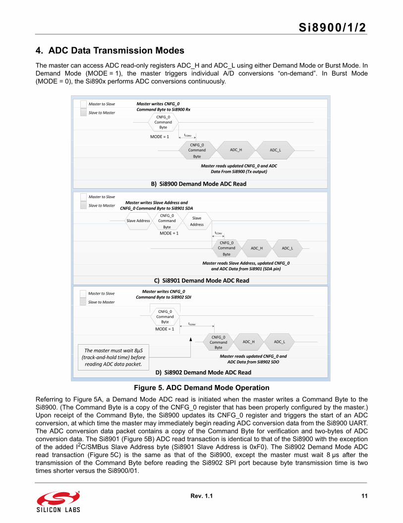
4. ADC Data Transmission ModesThe master can access ADC read-only registers ADC_H and ADC_L using either Demand Mode or Burst Mode. InDemand Mode (MODE = 1), the master triggers individual A/D conversions “on-demand”. In Burst Mode(MODE = 0), the Si890x performs ADC conversions continuously.
Figure 5. ADC Demand Mode OperationReferring to Figure 5A, a Demand Mode ADC read is initiated when the master writes a Command Byte to theSi8900. (The Command Byte is a copy of the CNFG_0 register that has been properly configured by the master.)Upon receipt of the Command Byte, the Si8900 updates its CNFG_0 register and triggers the start of an ADCconversion, at which time the master may immediately begin reading ADC conversion data from the Si8900 UART.The ADC conversion data packet contains a copy of the Command Byte for verification and two-bytes of ADCconversion data. The Si8901 (Figure 5B) ADC read transaction is identical to that of the Si8900 with the exceptionof the added I2C/SMBus Slave Address byte (Si8901 Slave Address is 0xF0). The Si8902 Demand Mode ADCread transaction (Figure 5C) is the same as that of the Si8900, except the master must wait 8 µs after thetransmission of the Command Byte before reading the Si8902 SPI port because byte transmission time is twotimes shorter versus the Si8900/01.
C) Si8901 Demand Mode ADC Read
B) Si8900 Demand Mode ADC Read
Master to Slave
Slave to MasterCNFG_0Command
Byte
tCONV
Master writes CNFG_0 Command Byte to Si8900 Rx
Master reads updated CNFG_0 and ADC Data From Si8900 (Tx output)
MODE = 1
ADC_H ADC_LCNFG_0Command
Byte
Master to Slave
Slave to Master
Master reads Slave Address, updated CNFG_0 and ADC Data from Si8901 (SDA pin)
MODE = 1
ADC_H
tCONV
ADC_L
CNFG_0Command
Byte
CNFG_0Command
Byte
CNFG_0Command
Byte tCONV
D) Si8902 Demand Mode ADC Read
Master writes CNFG_0 Command Byte to Si8902 SDI
Master reads updated CNFG_0 and ADC Data from Si8902 SDO
Master to Slave
Slave to Master
MODE = 1
ADC_H ADC_LCNFG_0 Command
Byte
Slave Address
Master writes Slave Address and CNFG_0 Command Byte to Si8901 SDA
The master must wait 8µS (track‐and‐hold time) before reading ADC data packet.
Slave
Address
Si8900/1/2
12 Rev. 1.1
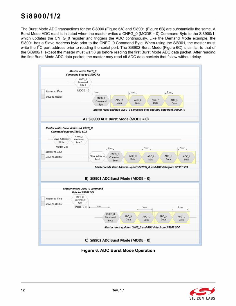
The Burst Mode ADC transactions for the Si8900 (Figure 6A) and Si8901 (Figure 6B) are substantially the same. ABurst Mode ADC read is initiated when the master writes a CNFG_0 (MODE = 0) Command Byte to the Si8900/1,which updates the CNFG_0 register and triggers the ADC continuously. Like the Demand Mode example, theSi8901 has a Slave Address byte prior to the CNFG_0 Command Byte. When using the Si8901, the master mustwrite the I2C port address prior to reading the serial port. The Si8902 Burst Mode (Figure 6C) is similar to that ofthe Si8900/1, except the master must wait 8 µs before reading the first Burst Mode ADC data packet. After readingthe first Burst Mode ADC data packet, the master may read all ADC data packets that follow without delay.
Figure 6. ADC Burst Mode Operation
A) Si8900 ADC Burst Mode (MODE = 0)
Master to Slave
Slave to Master
CNFG_0Command Byte 0
tCONV
Master writes CNFG_0 Command Byte to Si8900 Rx
Master reads updated CNFG_0 Command Byte and ADC data from Si8900 Tx
MODE = 0
ADC_HData
ADC_LData
ADC_HData
ADC_LData
tCONV
CNFG_0 Command
Byte
tCONV
B) Si8901 ADC Burst Mode (MODE = 0)
Master to Slave
Slave to Master
MODE = 0 tCONV
Master reads Slave Address, updated CNFG_0 and ADC data from Si8901 SDA
ADC_HData
ADC_LData
ADC_HData
ADC_LData
tCONV tCONV
CNFG_0Command Byte 0
CNFG_0 Command
Byte
Master writes Slave Address & CNFG_0 Command Byte to Si8901 SDA
Slave AddressRead
Slave Addrress Write
C) Si8902 ADC Burst Mode (MODE = 0)
Master to Slave
Slave to Master
Master writes CNFG_0 Command Byte to Si8902 SDI
CNFG_0Command
Byte
Master reads updated CNFG_0 and ADC data from Si8902 SDO
MODE = 0
ADC_HData
ADC_LData
ADC_HData
ADC_LData
CNFG_0Command
Byte
tCONV tCONVtCONV

Si8900/1/2
Rev. 1.1 13
4.1. UART (Si8900)The UART is a two-wire interface (Tx, Rx) and operates as an asynchronous, full-duplex serial port with internalauto baud rate generator that measures the period of incoming data stream and automatically adjusts the internalbaud rate generator to match. The auto baud rate detection and matching optimizes UART timing for minimum biterror rate. For more information, see “AN635: AC Line Monitoring Using the Si890x Family of Isolated ADCs”.There are a total of 10 bits per data read/write: One start bit, eight data bits (LSB first), and one stop bit with datatransmitted LSB first as shown in Figure 7. Figure 8A and Figure 8B show master/Si8900 ADC read transactionsfor Demand Mode and Burst Mode, respectively.
Figure 7. UART Data Byte
Figure 8. Si8900 ADC Read Operation
D7D6D5D4D3D2D1D0Start BitMARK
SPACE
BIT TIMES
BIT SAMPLING
STOP BIT
Master to Slave
Slave to Master
A) Si8900 Demand Mode ADC Read
D0 D1 D2 D3 D4 D5 D6 D7 D0 D1 D2 D3 D4 D5 D6 D7
STOP
START
START
STOPD0 D1 D2 D3 D4 D5 D6 D7
STOP
START
S
START
P
CNFG_0 Write Command Byte
B) Si8900 Burst Mode ADC Read
START
STOP
D0 D1 D2 D3 D4 D5 D6 D7
CNFG_0 Read Data STOP
START
STOP
START
Periodic ADC Data
CNFG_0 Read Data
ADC Data
D0 D1 D2 D3 D4 D5 D6 D7 D0 D1 D2 D3 D4 D5 D6 D7 D0 D1 D2 D3 D4 D5 D6 D7 D0 D1 D2 D3 D4 D5 D6 D7
S P
D0 D1 D2 D3 D4 D5 D6 D7
CNFG_0 Write Command Byte
STOP
START
STOP
START
STOP
START
D0 D1 D2 D3 D4 D5 D6 D7
‐
MX1
MODE = 1
MX0
PGA
11
VREF
‐
MX1
MODE=0
MX0
PGA
11
VREF
SS P P S SP
VREF
MX0
PGA
MODE = 0
MX1
‐ 11 D9 0 1
MX0
MX1
D8
D7
D6
D1
D0 00 D5
D4
D3
D2 P SD9 0 1
MX0
MX1
D8
D7
D6
S P SS P SD9 0 1
MX0
MX1
D8
D7
D6
D1
D0 00 D5
D4
D3
D2
MX0
PGA
MODE = 1
MX1
11
VREF‐
STOP
START
SPD1
D0 00 D5
D4
D3
D2

Si8900/1/2
14 Rev. 1.1
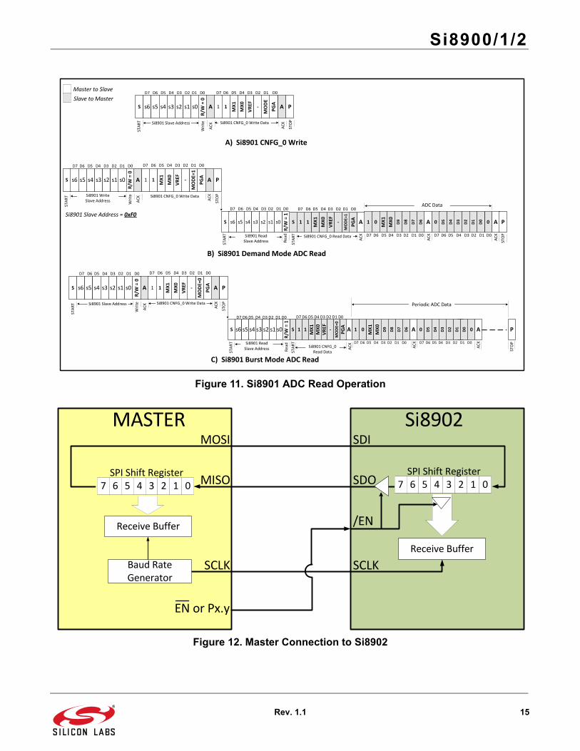
4.2. I2C/SMBus (Si8901)The I2C/SMBus serial port is a two-wire serial bus where data line SDA is bidirectional and clock line SCL isunidirectional. Reads and writes to this interface by the master are byte-oriented, with the I2C/SMBus mastercontrolling the serial data rates up to 240 kbps. The SDA and SCL lines must be pulled high through pull-upresistors of 5 k or less. An Si8901 ADC read transaction begins with a START condition (“S” or Repeated STARTcondition “SR”), which is defined as a high-to-low transition on SDA while SCL is high (Figure 9). The masterterminates a transmission with a STOP condition (P), defined as a low-to-high transition on SDA while SCL is high.The data on SDA must remain stable during the high period of the SCL clock pulse because such changes in eitherline will be interpreted as a control command (e.g., S, P SR). SDA and SCL idle in the high state when the bus isnot busy. Acknowledge bits (Figure 10) provide detection of successful data transfers, whereas unsuccessfultransfers conclude with a not-acknowledge bit (NACK). Both the master and the Si8901 generate ACK and NACKbits. An ACK bit is generated when the receiving device pulls SDA low before the rising edge of the acknowledgedrelated (ninth) SCL pulse and maintains it low during the high period of the clock pulse. A NACK bit is generatedwhen the receiver allows SDA to be pulled high before the rising edge of the acknowledged related SCL pulse andmaintains it high during the high period of the clock pulse. An unsuccessful data transfer occurs if a receivingdevice is busy or if a system fault has occurred. In the event of an unsuccessful data transfer, the bus masterattempts communication at a later time. Figure 11A shows the I2C Slave Address Byte and CNFG_0 byte for theSi8901. Figure 11B and Figure 11C show master/Si8901 ADC read transactions for Demand Mode and BurstMode, respectively.
Figure 9. Start and Stop Conditions
Figure 10. Acknowledge Cycle
SDA
SCL
S SR P
SDA
SCL
S Not Acknowledge (NACK)
Acknowledge (ACK)
1 2 9
Si8900/1/2
Rev. 1.1 15
Figure 11. Si8901 ADC Read Operation
Figure 12. Master Connection to Si8902
Master to Slave
Slave to Master
A) Si8901 CNFG_0 Write
B) Si8901 Demand Mode ADC Read
S s6 s5 s4 s3 s2 s1 A 1 A
START
ACK
ACKSi8901 CNFG_0 Write Data
Write
MX0
PGA
P
VREF
STOP
R/W
= 0
D7 D6 D5 D4 D3 D2 D1 D0
MX1
MODE
1
D7 D6 D5 D4 D3 D2 D1 D0
ACK
ADC Data
STOP
ACKD7 D6 D5 D4 D3 D2 D1 D0 D7 D6 D5 D4 D3 D2 D1 D0
C) Si8901 Burst Mode ADC Read
Si8901 Slave Address
s0
ACKSi8901 CNFG_0 Read Data
D7 D6 D5 D4 D3 D2 D1 D0
S s6 s5 s4 s3 s2 s1 A A
START
ACK
ACKSi8901 CNFG_0 Write Data
Write
P
STOP
R/W
= 0
D7 D6 D5 D4 D3 D2 D1 D0D7 D6 D5 D4 D3 D2 D1 D0
Si8901 Write Slave Address
s0
START
ACK
ACKSi8901 CNFG_0 Write Data
Write
STOP
D7 D6 D5 D4 D3 D2 D1 D0D7 D6 D5 D4 D3 D2 D1 D0
Si8901 Slave Address
STOP
Si8901 Slave Address = 0xF0
START
Read
D7 D6 D5 D4 D3 D2 D1 D0
Si8901 Read Slave Address
START
ACK
ACKD7 D6 D5 D4 D3 D2 D1 D0 D7 D6 D5 D4 D3 D2 D1 D0
ACK
Si8901 CNFG_0 Read Data
D7 D6 D5 D4 D3 D2 D1 D0
Periodic ADC Data
P
START
Read
D7 D6 D5 D4 D3 D2 D1 D0
Si8901 Read Slave Address
START
‐
1
MX0
PGA
VREF
MX1
MODE=1
1 ‐
A A0 0 0 P
MX1
MX0
D9
D8 AD7
D6
D5
D4
D3
D2
D1
D0S 1
MX0
PGA
VREF
MX1
MODE=1
1S s6 s5 s4 s3 s2 s1
R/W
= 1
s0 ‐ 1
S 1 A
MX0
PGA
VREF
MX1
MODE=0
1 AS s6 s5 s4 s3 s2 s1
R/W
= 1
s0 ‐ 0 0 0
MX1
MX0
D9
D8 AD7
D6
D5
D4
D3
D2
D1
D01 A
S s6 s5 s4 s3 s2 s1 A A P
R/W
= 0
s0 1
MX0
PGA
VREF
MX1
MODE=0
1 ‐
MASTER Si8902MOSI
MISO
SCLK
SDI
SDO
SCLK
/EN
7 6 5 4 3 2 1 0SPI Shift Register
Receive Buffer
Baud Rate Generator
EN or Px.y
7 6 5 4 3 2 1 0SPI Shift Register
Receive Buffer

Si8900/1/2
16 Rev. 1.1
4.3. SPI Port (Si8902)
Figure 13. Si8902 Data/Clock TimingThe Serial Peripheral Interface (SPI port) is a slave mode, full-duplex, synchronous, 4-wire serial bus that connectsto the master as shown in Figure 12. The master's clock and data timing must match the Si8902 timing shownFigure 12 (for more information about clock and data timing, please see the “SPI Port” section of Table 2 onpage 6).As shown in Figure 13, an SPI bus transaction begins with the master driving EN low and maintaining this state forthe duration of the read transaction(s). The master transmits data from its master-out/slave-in terminal (MOSI) tothe Si8902 serial read/write input terminal (SDI). The Si8902 transmits data to the master from its serial data-outterminal (SDO) to the master-in/slave-out terminal (MISO), and data transfer ends when the master returns /EN tothe high state. Figure 14A shows the Si8902 CNFG_0 Command Byte format, while Figures 14B and 14C showSi8902 Demand Mode and Burst Mode ADC reads.
MSB Bit 6 Bit 5 Bit 4 Bit 3 Bit 2 Bit 1 Bit 0
MSB Bit 6 Bit 5 Bit 4 Bit 3 Bit 2 Bit 1 Bit 0
SCLK
SDI
SDO
EN

Si8900/1/2
Rev. 1.1 17
Figure 14. Si8902 ADC Read Operation
4.4. Master Controller Firmware The user's master controller must include firmware to manage the Si890x Demand and Burst operating modes andserial port control. In some cases, the master controller may also require a firmware moving average function toreduce noise. For more information on master controller firmware, see “AN637: Si890x Master ControllerRecommendations”, available for download at www.silabs.com/isolation.
Master to Slave
Slave to Master
B) Si8902 ADC Demand Mode Read
ADC Data
1 0
MX1
MX0
D9
D8
D7
D6
D5
D4
D3
D2
D1
D0
D7 D6 D5 D4 D3 D2 D1 D0
A) Si8902 CNFG_0 Command Byte
CNFG_0 Write Command Byte
D7 D6 D5 D4 D3 D2 D1 D0
C) Si8902 ADC Burst Mode Read
Si8902 CNFG_0 Read Byte
D7 D6 D5 D4 D3 D2 D1 D0
CNFG_0 Write Command Byte
MX0
PGA
VREF
D7 D6 D5 D4 D3 D2 D1 D0
MX1
MODE
11
D7 D6 D5 D4 D3 D2 D1 D0
Periodic ADC Data
CNFG_0 Write Command Byte
Si8902 CNFG_0 Read Byte
‐MX0
PGA
VREF
MX1
MODE=1
11 ‐
MX0
PGA
VREF
MX1
MODE = 1
1 ‐1 0 0
MX0
PGA
VREF
MX1
MODE=0
11 ‐
D7 D6 D5 D4 D3 D2 D1 D0
8µS Delay
8µS Delay D7 D0 D7 D0
1
MX1
MX0
D9
D8
D7
D60 0 D5
D4
D3
D2
D1
D0 01
MX1
MX0
D9
D8
D7
D6
MX0
PGA
VREF
MX1
MODE = 0
1 ‐1 0 0 D5
D4
D3
D2
D1
D0 0
D7 D0 D7 D0 D7 D0
Si8900/1/2
18 Rev. 1.1
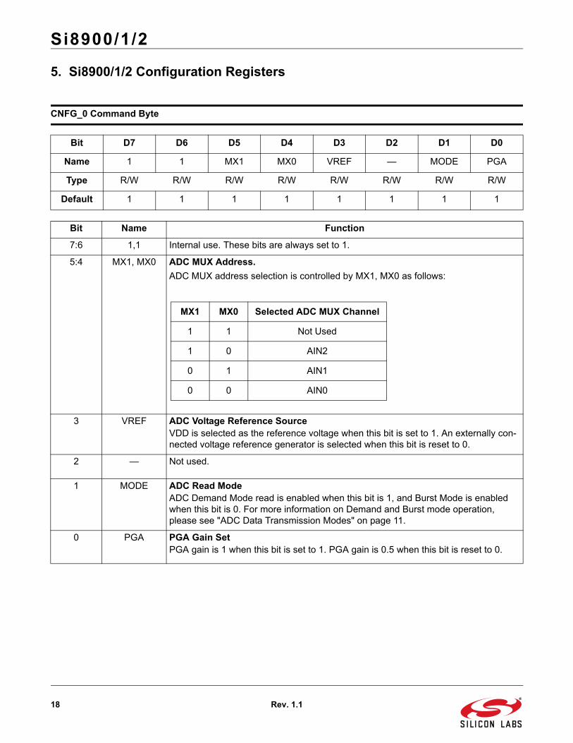
5. Si8900/1/2 Configuration Registers
CNFG_0 Command Byte
Bit D7 D6 D5 D4 D3 D2 D1 D0
Name 1 1 MX1 MX0 VREF — MODE PGA
Type R/W R/W R/W R/W R/W R/W R/W R/W
Default 1 1 1 1 1 1 1 1
Bit Name Function
7:6 1,1 Internal use. These bits are always set to 1.
5:4 MX1, MX0 ADC MUX Address.ADC MUX address selection is controlled by MX1, MX0 as follows:
3 VREF ADC Voltage Reference SourceVDD is selected as the reference voltage when this bit is set to 1. An externally con-nected voltage reference generator is selected when this bit is reset to 0.
2 — Not used.
1 MODE ADC Read ModeADC Demand Mode read is enabled when this bit is 1, and Burst Mode is enabled when this bit is 0. For more information on Demand and Burst mode operation, please see "ADC Data Transmission Modes" on page 11.
0 PGA PGA Gain SetPGA gain is 1 when this bit is set to 1. PGA gain is 0.5 when this bit is reset to 0.
MX1 MX0 Selected ADC MUX Channel
1 1 Not Used
1 0 AIN2
0 1 AIN1
0 0 AIN0
Si8900/1/2
Rev. 1.1 19
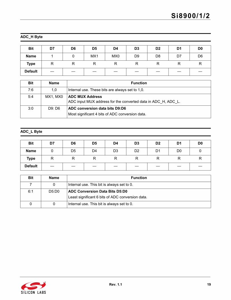
ADC_H Byte
Bit D7 D6 D5 D4 D3 D2 D1 D0
Name 1 0 MX1 MX0 D9 D8 D7 D6
Type R R R R R R R R
Default — — — — — — — —
Bit Name Function
7:6 1,0 Internal use. These bits are always set to 1,0.
5:4 MX1, MX0 ADC MUX AddressADC input MUX address for the converted data in ADC_H, ADC_L.
3:0 D9: D6 ADC conversion data bits D9:D6Most significant 4 bits of ADC conversion data.
ADC_L Byte
Bit D7 D6 D5 D4 D3 D2 D1 D0
Name 0 D5 D4 D3 D2 D1 D0 0
Type R R R R R R R R
Default — — — — — — — —
Bit Name Function
7 0 Internal use. This bit is always set to 0.
6:1 D5:D0 ADC Conversion Data Bits D5:D0Least significant 6 bits of ADC conversion data.
0 0 Internal use. This bit is always set to 0.
Si8900/1/2
20 Rev. 1.1
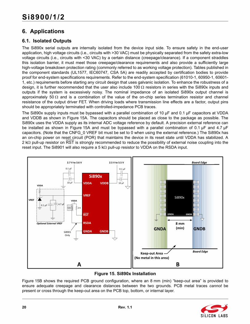
6. Applications6.1. Isolated OutputsThe Si890x serial outputs are internally isolated from the device input side. To ensure safety in the end-userapplication, high voltage circuits (i.e., circuits with >30 VAC) must be physically separated from the safety extra-lowvoltage circuits (i.e., circuits with <30 VAC) by a certain distance (creepage/clearance). If a component straddlesthis isolation barrier, it must meet those creepage/clearance requirements and also provide a sufficiently largehigh-voltage breakdown protection rating (commonly referred to as working voltage protection). Tables published inthe component standards (UL1577, IEC60747, CSA 5A) are readily accepted by certification bodies to provideproof for end-system specifications requirements. Refer to the end-system specification (61010-1, 60950-1, 60601-1, etc.) requirements before starting any circuit design that uses galvanic isolation. To enhance the robustness of adesign, it is further recommended that the user also include 100 resistors in series with the Si890x inputs andoutputs if the system is excessively noisy. The nominal impedance of an isolated Si890x output channel isapproximately 50 and is a combination of the value of the on-chip series termination resistor and channelresistance of the output driver FET. When driving loads where transmission line effects are a factor, output pinsshould be appropriately terminated with controlled-impedance PCB traces.The Si890x supply inputs must be bypassed with a parallel combination of 10 µF and 0.1 µF capacitors at VDDAand VDDB as shown in Figure 15A. The capacitors should be placed as close to the package as possible. TheSi890x uses the VDDA supply as its internal ADC voltage reference by default. A precision external reference canbe installed as shown in Figure 15A and must be bypassed with a parallel combination of 0.1 µF and 4.7 µFcapacitors. (Note that the CNFG_0 VREF bit must be set to 0 when using the external reference.) The Si890x hasan on-chip power on reset circuit (POR) that maintains the device in its reset state until VDDA has stabilized. A2 k pull-up resistor on RST is strongly recommended to reduce the possibility of external noise coupling into thereset input. The Si8901 will also require a 5 k pull-up resistor to VDDA on the RSDA input.
Figure 15. Si890x InstallationFigure 15B shows the required PCB ground configuration, where an 8 mm (min) “keep-out area” is provided toensure adequate creepage and clearance distances between the two grounds. PCB metal traces cannot bepresent or cross through the keep-out area on the PCB top, bottom, or internal layer.
Si890x
GNDA GNDB
0.1 µF 4.7 µF
VDDA
Si890x
VREF
RST
RSDA
VDDA
GNDA
VDDB
GNDB
VREF
2 K
VDDA
5 K
Si8901 Only
0.1 µF
10 µF
2.7 V to 3.6 V
0.1 µF
10 µF
2.5 V to 5.5 V
8 mm (min) GNDB GNDA
Keep‐out Area(No metal in this area)
Board Edge
Board Edge
A B
Optional External VREF

Si8900/1/2
Rev. 1.1 21
6.2. Device ResetDuring power-up, the Si890x is held in the reset state by the internal power-on reset signal (POR) until VDDAsettles above VRST. When this condition is met, a delay is initiated that maintains the Si890x in the reset state fortime period tPOR, after which the reset signal is driven high allowing the Si890x to start-up. Note the maximumallowable VDD ramp time (i.e. time from 0 V to VDDA settled above VRST) is 1 ms. Slower ramp times may causethe Si890x to be released from reset before VDDA reaches the VRST level.Figure 16 shows typical VDDA monitor reset timing where the internal reset is driven low (Si890x in reset) whenVDDA falls below VRST (e.g., during a power down or VDDA brownout). The internal reset is released to its highstate when VDDA again settles above VRST. External circuitry can also be used to force a reset event by drivingthe external RST input low. A 2 k pull-up resistor on RST is recommended to avoid erroneous reset events fromexternal noise coupling to the RST input.
Figure 16. Si890x Power-on and Monitor Reset
VDDA Monitor ResetPower‐On Reset
tPOR
VRSTH
VDDA
VDDA(min)
VDDA
VRSTL
Internal RESET

Si8900/1/2
22 Rev. 1.1
6.3. Application ExampleFigure 17 shows the Si8900 operating as a single-phase ac line voltage and current monitor. The VDDA dc biascircuit uses a low-cost 3.3 V linear regulator referenced to the neutral (white wire). The ac current is measured onADC input AIN0. The ac line voltage is scaled by resistors R17 and R18 and level-shifted by the 1.5 V VREF. ACline current is measured using differential amplifier U1 connected across shunt resistor R1. Data is transferred tothe external controller or processor via the isolated UART.
Figure 17. AC Line Monitor Application Example
U1Low Cost
Dual OpAmp
R1
C1
U23.3 V LDO
C4 C5
Si8900AIN0
VDDA
GNDA
AIN1
WHITE
BLACK
D1
TX
RX
VDDB
GNDB
External Master Controller
Output Side Bias Supply
C2
1.5 V
R2 R3
R6
R5
R7
R8R9
1.5 V
R11
C3
1.5 V
R12
R13R14
R15
R4
Single‐PhaseAC Line
R10
R17
R18
Si8900/1/2
Rev. 1.1 23
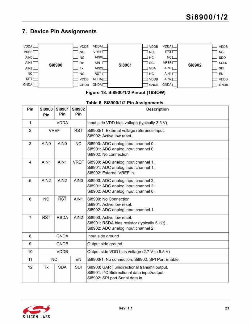
7. Device Pin Assignments
Figure 18. Si8900/1/2 Pinout (16SOW)
Table 6. Si8900/1/2 Pin AssignmentsPin Si8900
PinSi8901
PinSi8902
PinDescription
1 VDDA Input side VDD bias voltage (typically 3.3 V)
2 VREF RST Si8900/1: External voltage reference input.Si8902: Active low reset.
3 AIN0 AIN0 NC Si8900: ADC analog input channel 0.Si8901: ADC analog input channel 0.Si8902: No connection
4 AIN1 AIN1 VREF Si8900: ADC analog input channel 1.Si8901: ADC analog input channel 1.Si8902: External VREF in.
5 AIN2 AIN2 AIN0 Si8900: ADC analog input channel 2.Si8901: ADC analog input channel 2.Si8902: ADC analog input channel 0.
6 NC RST AIN1 Si8900: No Connection.Si8901: Active low reset.Si8902: ADC analog input channel 1.
7 RST RSDA AIN2 Si8900: Active low reset.Si8901: RSDA bias resistor (typically 5 k).Si8902: ADC analog input channel 2.
8 GNDA Input side ground
9 GNDB Output side ground
10 VDDB Output side VDD bias voltage (2.7 V to 5.5 V)
11 NC EN Si8900/1: No connection. Si8902: SPI Port Enable.
12 Tx SDA SDI Si8900: UART unidirectional transmit output.Si8901: I2C Bidirectional data input/output.Si8902: SPI port Serial data in.
AIN2
VDDB
NC
NCRx
Tx
NC
VDDB
GNDB
Si8900
VDDA
VREF
AIN0AIN1
NC
RST
GNDA
VDDB
NC
NCSCL
SDA
NC
VDDB
GNDB
Si8901
VDDA
VREF
RST
AIN0
AIN1
AIN2
RSDA
GNDA
VDDB
NC
SDOSCLK
SDI
EN
VDDB
GNDB
Si8902
VDDA
RST
NCVREF
AIN0
AIN1
AIN2
GNDA

Si8900/1/2
24 Rev. 1.1
13 Rx SCL SCLK Si8900: UART unidirectional receive input.Si8901: I2C port unidirectional serial clock input.Si8902: SPI port unidirectional serial clock input.
14 NC SDO Si8900/1: No connection.Si8902: SPI port Serial data out (SDO)
15 NC No connection
16 VDDB Si8900/1/2: Output side VDD bias voltage (2.7 V to 5.5 V).
Table 6. Si8900/1/2 Pin Assignments (Continued)Pin Si8900
PinSi8901
PinSi8902
PinDescription

Si8900/1/2
Rev. 1.1 25
8. Ordering Guide
Table 7. Product Ordering Information1,2,3
Part Number (OPN) Serial Port Package Isolation Rating Temp Range
Si8900B-A01-GS UART WB SOIC 2.5 kV –40 to +85 °C
Si8900D-A01-GS UART WB SOIC 5.0 kV –40 to +85 °C
Si8901B-A01-GS I2C/SMBus WB SOIC 2.5 kV –40 to +85 °C
Si8901D-A01-GS I2C/SMBus WB SOIC 5.0 kV –40 to +85 °C
Si8902B-A01-GS SPI Port WB SOIC 2.5 kV –40 to +85 °C
Si8902D-A01-GS SPI Port WB SOIC 5.0 kV –40 to +85 °C
Notes:1. Add an “R” suffix to the part number to specify the tape and reel option. Example: “Si8900AB-A-ISR”.2. All packages are RoHS-compliant.3. Moisture sensitivity level is MSL3 for wide-body SOIC-16 package with peak reflow temperatures of 260 °C according
to the JEDEC industry standard classifications and peak solder temperatures.

Si8900/1/2
26 Rev. 1.1
9. Package Outline: 16-Pin Wide Body SOICFigure 19 illustrates the package details for the Si8900/1/2 Digital Isolator. Table 8 lists the values for thedimensions shown in the illustration.
Figure 19. 16-Pin Wide Body SOIC

Si8900/1/2
Rev. 1.1 27
Table 8. Package Diagram Dimensions
SymbolMillimeters
Min MaxA — 2.65
A1 0.10 0.30
A2 2.05 —
b 0.31 0.51
c 0.20 0.33
D 10.30 BSC
E 10.30 BSC
E1 7.50 BSC
e 1.27 BSC
L 0.40 1.27
h 0.25 0.75
θ 0° 8°
aaa — 0.10
bbb — 0.33
ccc — 0.10
ddd — 0.25
eee — 0.10
fff — 0.20
Notes:1. All dimensions shown are in millimeters (mm) unless otherwise
noted.2. Dimensioning and Tolerancing per ANSI Y14.5M-1994.3. This drawing conforms to JEDEC Outline MS-013, Variation AA.4. Recommended reflow profile per JEDEC J-STD-020C specification
for small body, lead-free components.

Si8900/1/2
28 Rev. 1.1
10. Land Pattern: 16-Pin Wide-Body SOICFigure 20 illustrates the recommended land pattern details for the Si8900/1/2 in a 16-pin wide-body SOIC. Table 9lists the values for the dimensions shown in the illustration.
Figure 20. 16-Pin SOIC Land Pattern
Table 9. 16-Pin Wide Body SOIC Land Pattern Dimensions
Dimension Feature (mm)
C1 Pad Column Spacing 9.40
E Pad Row Pitch 1.27
X1 Pad Width 0.60
Y1 Pad Length 1.90
Notes:1. This Land Pattern Design is based on IPC-7351 pattern SOIC127P1032X265-16AN
for Density Level B (Median Land Protrusion).2. All feature sizes shown are at Maximum Material Condition (MMC) and a card
fabrication tolerance of 0.05 mm is assumed.

Si8900/1/2
Rev. 1.1 29
11. Top Marking: 16-Pin Wide Body SOIC11.1. Si8900/1/2 Top Marking
11.2. Top Marking Explanation
Line 1 Marking:
Base Part Number Ordering Options
(See Ordering Guide for more information).
Si890 = Isolator product seriesX = Serial Port
0 = UART1 = I2C2 = SPI
Y = Insulation ratingB = 2.5 kV; D = 5.0 kV
Line 2 Marking:
YY = YearWW = Workweek
Assigned by assembly subcontractor. Corresponds to the year and workweek of the mold date.
RTTTTT = Mfg Code Manufacturing code from assembly house“R” indicates revision
Line 3 Marking:
Circle = 1.7 mm Diameter(Center-Justified) “e4” Pb-Free Symbol
Country of Origin ISO Code Abbreviation TW = Taiwan
Si890XYYYWWRTTTTT
TW e4
Si8900/1/2
30 Rev. 1.1
DOCUMENT CHANGE LIST
Revision 0.5 to Revision 1.0 No changes.
Revision 1.0 to Revision 1.1 Removed “pending” throughout. Changed AN638 reference to AN637. Updated "Top Marking: 16-Pin Wide Body SOIC" on
page 29.
Si8900/1/2
Rev. 1.1 31
NOTES:

DisclaimerSilicon Laboratories intends to provide customers with the latest, accurate, and in-depth documentation of all peripherals and modules available for system and software implementers using or intending to use the Silicon Laboratories products. Characterization data, available modules and peripherals, memory sizes and memory addresses refer to each specific device, and "Typical" parameters provided can and do vary in different applications. Application examples described herein are for illustrative purposes only. Silicon Laboratories reserves the right to make changes without further notice and limitation to product information, specifications, and descriptions herein, and does not give warranties as to the accuracy or completeness of the included information. Silicon Laboratories shall have no liability for the consequences of use of the information supplied herein. This document does not imply or express copyright licenses granted hereunder to design or fabricate any integrated circuits. The products must not be used within any Life Support System without the specific written consent of Silicon Laboratories. A "Life Support System" is any product or system intended to support or sustain life and/or health, which, if it fails, can be reasonably expected to result in significant personal injury or death. Silicon Laboratories products are generally not intended for military applications. Silicon Laboratories products shall under no circumstances be used in weapons of mass destruction including (but not limited to) nuclear, biological or chemical weapons, or missiles capable of delivering such weapons.
Trademark InformationSilicon Laboratories Inc., Silicon Laboratories, Silicon Labs, SiLabs and the Silicon Labs logo, CMEMS®, EFM, EFM32, EFR, Energy Micro, Energy Micro logo and combinations thereof, "the world’s most energy friendly microcontrollers", Ember®, EZLink®, EZMac®, EZRadio®, EZRadioPRO®, DSPLL®, ISOmodem ®, Precision32®, ProSLIC®, SiPHY®, USBXpress® and others are trademarks or registered trademarks of Silicon Laboratories Inc. ARM, CORTEX, Cortex-M3 and THUMB are trademarks or registered trademarks of ARM Holdings. Keil is a registered trademark of ARM Limited. All other products or brand names mentioned herein are trademarks of their respective holders.
http://www.silabs.com
Silicon Laboratories Inc.400 West Cesar ChavezAustin, TX 78701USA
Smart.Connected.Energy-Friendly
Productswww.silabs.com/products
Qualitywww.silabs.com/quality
Support and Communitycommunity.silabs.com