signal processing and data transmission using … · jorge cervera signal processing and data...
TRANSCRIPT

Jorge Cervera Signal Processing and Data Transmission using a FPGA
1
SIGNAL PROCESSING AND DATA TRANSMISSION USING
A FPGA
Autor: Jorge Cervera
Tutors: Baran Cürüklü.
University: Mälardalens Hogskola (Västerås, SWEDEN).
Home University: Escuela Universitaria de La Almunia de Doña Godina (Zaragoza, España)
Date: Spring Semester 2008.

Jorge Cervera Signal Processing and Data Transmission using a FPGA
2
ABSTRACT:
This thesis work has three main parts: the first one is to implement the hardware design of a FPGA capable of reading in parallel 64 digital signals and process them. The second part is about implementing a component that allows a PC machine to interact with a FPGA. In the third part, both components will be assembled in the final design.
First of all, an overview of the FPGA technologies, and its main developers and suppliers is given to provide a major understanding of how this technology works. Then the two main HDL languages and their characteristics are explained. The design tools used to develop the project are then showed before the explanation of the development of this first part of the project; After that, in the first part of the project a suitable design to process a digital signal generated by a square array of 8×8 ITO electrodes photo lithographically defined in a 0.5_m thick photoresist layer previously filtered amplified and converted to digital electronically is going to be implemented step by step. In the second part is about an attempt to create an interface between the FPGA and a PC machine. This interface should be able to “order” the FPGA to record data and then send them to the PC. As a final part, those two components will be assembled and tested to give the final design, a design capable of reading, processing and sending the signals received from the electrodes to a PC machine. Once this design is finished and tested, the characteristics that the FPGA needs to have to perform all the needed functions will be known. The main purpose is to find a FPGA that can manage to process 64 signals in parallel so all the tests and results can be taken in the same time lapse. Rather than focusing on hardware programming, finding a FPGA fast enough and with the required amount of memory and pins is the aim of the document. The results of a simple test run and simulated in each device is shown, besides of the description of the implementation of the interface.
Jorge Cervera Signal Processing and Data Transmission using a FPGA
3
Acknowledgements:
First acknowledgements are for all my family, specially to my mother Mª Dolores, because thanks to you and to your effort I am where I am and I am what I am. To my sister Mará you made my childhood a wonderful time and for being my best friend now. To my sisters Nuria and Idoya, mothers and sisters at one time, thank you for your patience. To my niece Sara, because with less than one year you have taught me to fight. To Nadia and Sheila, my crazy nieces. And to my father, because you tried to show me what I didn´t want to see, thank you for teaching me what is the bad way, although you are not here.
I don´t want to forget my friends: All my friends from La Salle, someday we will pass through the adolescence and we´ll be adults. To the people from the Ludoteque that taught me that Sparta does not retreat. And to all my friends in Sweden, the love brigade, the fellowship of the ring, the north troglodytes, the troll women and the girls from Madrid, Örebro, Västerås or Ibarrekolanda.
Thanks to all of you for supporting me and being there.
Agradecimientos:
Primero quiero agradecérselo a toda mi familia, en especial a mi madre, Mª Dolores, porque gracias a ti y a tu esfuerzo estoy donde estoy y soy quien soy. A mi hermana María por hacer de mi infancia una época maravillosa y por ser ahora mi mejor amiga. A mis hermanas Nuria e Idoya, que fuisteis madres y hermanas a un tiempo, gracias por vuestra paciencia. A mi sobrina Sara, porque con menos de un año tu me has enseñado lo que es luchar. A Nadia y Sheila, mis sobrinas que están aun mas locas que yo.Y a mi padre, por intentar hacerme ver lo que yo no quería, gracias por enseñarme cual es el mal camino, aunque ya no estés.
Tampoco quiero olvidar a mis amigos: todos los del colegio la Salle, algún día superaremos la pubertad y nos haremos adultos. A la gente de la Ludoteque, que me enseñó que Esparta no se retira. Y a todos mis amigos en Suecia, la brigada del amor, la comunidad del Anillo, los trogloditas del norte, las mujeres troll y sin olvidarme de las chicas de Madrid, Örebro, Västeras o Ibarrekolanda.
Gracias a todos por apoyarme y estar ahí.
Jorge Cervera Signal Processing and Data Transmission using a FPGA
4
Index
1. Background ...…………………………………………………………………………8
2. FPGAS ...……………………………………………………………………………...8
2.1. Historical Overview ...………………………………………………………8
2.2. Basic Functioning ...………………………………………………………...9
2.3. Developers ...………………………………………………………………10
2.3.1. Altera ………………………………………………………….....10
2.3.2 Xilinx ...…………………………………………………………..11
3. Hardware Description Languages ...………………………………………………...11
3.1. VHDL ...…………………………………………………………………...12
3.1.1.Program Structure ...……………………………………………...13
3.2. Verilog ...…………………………………………………………………..14
4. VHDL/Verilog Compared & Contrasted …………………………………………....15
5. Hardware Design and Simulating Tools ...…………………………………………..15
5.1. Altera’s Quartus II 7.2sp3 Web Edition ...………………………………...15
5.2. Xilinx’s ISE Design Suite 10.1. ..………………………………………….16
5.3. ModelSim PE Student Edition 6.3.c ……………………………………....16
5.4. Choosing a Design Tool …………………………………………………..16
6. Developing of the design …...……………………………………………………….16
6.1. First Part: Design of a system capable of receiving, processing and sending signals in a FPGA ……………………………………………………………...17
6.1.1. First Design ……………………………………………………...17
6.1.2. Second Design ...………………………………………………...19
6.1.3. Third Design …………………………………………………….21
6.1.4. Fourth Design ……………………………………………………23
6.1.5. Fifth Design ...…………………………………………………...27
6.2. Second Part: Design of a system capable of interact with a PC machine…………29

Jorge Cervera Signal Processing and Data Transmission using a FPGA
5
6.2.1. Hardware ………………………………………………………………..30
6.2.2. Transmitter Device ……………………………………………………...31
6.2.3. Receiver Device …………………………………………………………36
6.3. Third Part: Assembling of the three components …………………………………41
6.4. Final Test ………………………………………………………………………….46
7. Conclussions ………………………………………………………………………...48
7.1. Advantages ………………………………………………………………...49
7.2. Drawbacks ………………………………………………………………...49
7.3. Future Work ……………………………………………………………….49
8. References …………………………………………………………………………..50
Appendix A: The util package …………………………………………………………53
Appendix B: Time Planning …………………………………………………………...54

Jorge Cervera Signal Processing and Data Transmission using a FPGA
6
List of Figures
Figure 1: Basic Overview .................................................................................................8 Figure 2: Top FPGA 2007 suppliers ................................................................................9 Figure 3: Logic Cell .........................................................................................................9 Figure 4: Interconnection of Logic Blocks .....................................................................10 Figure 5: VHDL entities and architectures ....................................................................13 Figure 6: Verilog modules ..............................................................................................14 Figure 7: First Design ....................................................................................................18 Figure 8: First Design Code ..........................................................................................18 Figure 9: First Design Test ............................................................................................19 Figure 10: Second Design ..............................................................................................19 Figure 11: Second Design Code 1st Part .......................................................................20 Figure 12: Second Design Code 2nd Part ......................................................................20 Figure 13: Second Design Test ......................................................................................21 Figure 14: Third Design .................................................................................................22 Figure 15: Third Design Code .......................................................................................22 Figure 16: Third Design Test .........................................................................................23 Figure 17: Fourth Design................................................................................................23 Figure 18: Fourth Design Code Part 1...........................................................................24 Figure 19: Fourth Design Table of Signals ...................................................................24 Figure 20: Fourth Design Code Part 2 ..........................................................................25 Figure 21: Fourth Design Code Part 3 ..........................................................................26 Figure 22: Fourth Design Test .......................................................................................26 Figure 23: Fifth Design ..................................................................................................27 Figure 24: Fifth Design Code Part 1 .............................................................................27 Figure 25: Fifth Design Code Part 2 .............................................................................28 Figure 26: Fifth Design Test ..........................................................................................29 Figure 27: Male RS-232 plug .........................................................................................30 Figure 28: Female to Female DB-9 Cable .....................................................................30 Figure 29: Transmitter entity .........................................................................................31 Figure 30: Transmitter entity, constants and signals .....................................................32 Figure 31: Transmitter Table of Signals ........................................................................32 Figure 32: Transmitter Baud Generator ........................................................................33 Figure 33: Serializer State Machine ..............................................................................34 Figure 34: Multiplexor ...................................................................................................35 Figure 35: Transmitter Test ...........................................................................................36 Figure 36: Receiver Entity .............................................................................................37 Figure 37: Receiver Entity, Constants and Signals ........................................................37 Figure 38: Receiver Table of Signals .............................................................................37 Figure 39: Receiver Baud Generator .............................................................................38 Figure 40: D-Flip-Flop ..................................................................................................39 Figure 41: Received Data Filter ....................................................................................40 Figure 42: Receiver State Machine ................................................................................40 Figure 43: Receiver Shift Register .................................................................................40 Figure 44: Receiver Test ................................................................................................41 Figure 45: Final Design .................................................................................................42 Figure 46: Processor Entity ...........................................................................................42 Figure 47: Component Transmitter ................................................................................43
Jorge Cervera Signal Processing and Data Transmission using a FPGA
7
Figure 48: Component Receiver .....................................................................................43 Figure 49: Port Mapping ...............................................................................................43 Figure 50: Counter Signal with PC Start Order ............................................................44 Figure 51: Processing signals with PC start order ........................................................44 Figure 52: Stop Signal PC Order ...................................................................................44 Figure 53: Final Test, Record Code Received ...............................................................46 Figure 54: Final Test, Signal not Valid ..........................................................................47 Figure 55: Final Test, Valid Signal Recorded ...............................................................47 Figure 56: Final Test, Transmission Finished ...............................................................48 Figure 57: Package Util User Defined Types ................................................................51 Figure 58: Package Util Code .......................................................................................52 Figure 59: Time Planning...............................................................................................53
Jorge Cervera Signal Processing and Data Transmission using a FPGA
8
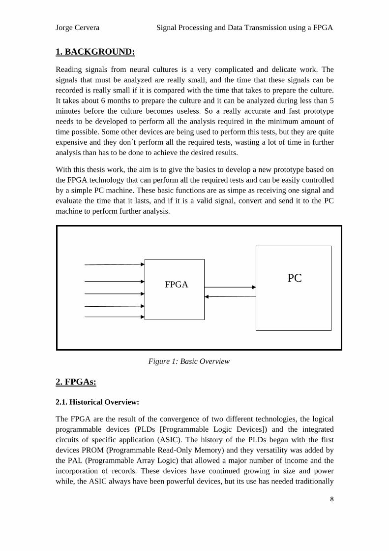
1. BACKGROUND:
Reading signals from neural cultures is a very complicated and delicate work. The signals that must be analyzed are really small, and the time that these signals can be recorded is really small if it is compared with the time that takes to prepare the culture. It takes about 6 months to prepare the culture and it can be analyzed during less than 5 minutes before the culture becomes useless. So a really accurate and fast prototype needs to be developed to perform all the analysis required in the minimum amount of time possible. Some other devices are being used to perform this tests, but they are quite expensive and they don´t perform all the required tests, wasting a lot of time in further analysis than has to be done to achieve the desired results.
With this thesis work, the aim is to give the basics to develop a new prototype based on the FPGA technology that can perform all the required tests and can be easily controlled by a simple PC machine. These basic functions are as simpe as receiving one signal and evaluate the time that it lasts, and if it is a valid signal, convert and send it to the PC machine to perform further analysis.
Figure 1: Basic Overview 2. FPGAs: 2.1. Historical Overview:
The FPGA are the result of the convergence of two different technologies, the logical programmable devices (PLDs [Programmable Logic Devices]) and the integrated circuits of specific application (ASIC). The history of the PLDs began with the first devices PROM (Programmable Read-Only Memory) and they versatility was added by the PAL (Programmable Array Logic) that allowed a major number of income and the incorporation of records. These devices have continued growing in size and power while, the ASIC always have been powerful devices, but its use has needed traditionally
FPGA
PC

Jorge Cervera Signal Processing and Data Transmission using a FPGA
9
a considerable investment of time and money. Attempts of reducing this load have come from the modularization of the elements of the circuits, as the ASIC based on cells, and from the standardization of the masks, as Ferranti was pioneering with the ULA (Uncommitted Logic Array). The final step was to combine both strategies with a mechanism of interconnection that could be programmed using fuses, antifuses or RAM cells, as the innovative devices Xilinx of middle of the 80. The resultant circuits are similar in capacity and applications to the biggest PLDs, though there are punctual differences that aim to different origins. Besides computation reconfigurable, the FPGAs are in use in controllers, coders/decoders, VLSI circuits’ prototyping.
The first manufacturer of these devices was Xilinx and Xilinx's devices are still the most popular devices. Other FPGA suppliers are Atmel, Actel, Altera and Lattice Semiconductor.
Figure 2: Top FPGA 2007 suppliers
2.2. Basic Functioning:
To build a FPGA, a basic "logic-cell" is duplicated hundreds or thousands of times. Basically this cells is a small lookup table ("LUT"), a D-flipflop and a 2-to-1 mux (to bypass the flipflop if desired).
Figure 3: Logic cell

Jorge Cervera Signal Processing and Data Transmission using a FPGA
10
A hierarchy of programmable interconnections allows the logical blocks of a FPGA to be interconnected according to the need of the designer of the system, something similar to a programmable breadboard. These logical blocks and interconnections can be programmed after the process of manufacture by the user / designer, so the FPGA can perform any logical necessary function.
Figure 4: Interconnection of logic blocks
A recent trend has been to combine the logical blocks and interconnections of the FPGA with microprocessors and peripheral related to form a “programmable System in a chip ". Example of such hybrid technologies they can be found in the devices Virtex-II PRO and Virtex-4 of Xilinx, which include one or more processors PowerPC absorbed together with the logic of the FPGA. Atmel's FPSLIC is another similar device, which uses a processor AVR in combination with Atmel's logical programmable architecture. Another alternative is use cores of implemented processors using the logic of the FPGA. These cores include the processors MicroBlaze and PicoBlaze de Xlinx, Nios and Nios II of Altera, and the processors of opened code LatticeMicro32 and LatticeMicro8.
Many modern FPGA support the partial reconfiguration of the system, allowing a part of the design to be rescheduled, while other parts continue working. This one is the principle of the “computation reconfigurable computation” idea.
2.3. Developers:
2.3.1. Altera:
Altera Corporation is the pioneer of programmable logic solutions. Today, Altera offers FPGAs, CPLDs, and structured ASICs in combination with software tools, intellectual property, and customer support to provide high-value programmable solutions. Altera is headquartered in San Jose, California, USA.

Jorge Cervera Signal Processing and Data Transmission using a FPGA
11
Altera´s devices can be divided in two main families: The Cyclone family and the Stratix family. The main difference between these two families is that Stratix FPGAs uses ALUTs instead of normal LUTs. Altera estimates than an ALUT to be equivalent to 2.5 LUTs. This makes Stratix FPGAs much better but more expensive that Cyclone ones.
2.3.2. Xilinx:
One of the world’s largest developers of FPGAs is Xilinx, Inc. It was founded in 1984 and was based in Silicon Valley. Today, their HQ resides in San Jose, California (U.S.); the European HQ is based in Dublin (Ireland) and the Asia Pacific/Japan HQ is based in Singapore.
Xilinx FPGAs can be divided in two main families: The Virtex family and the Spartan 3 family. The Virtex family targets high performance applications that require higher clock rates, extensive math operations, or significant use of single cycle timed loops. The Spartan 3 family is intended for higher volume applications and as such has some tradeoffs when it comes to the number of resources available on the chip as well as over-all performance. The Spartan 3 resource mix works well for applications that require more logic operations and rely less heavily on specialty resources
3. Hardware Description Languages:
In previous decades, most logic design was performed graphically, using block diagrams and schematics. However, the rise of synthesizable HDLs coupled with programmable logic devices and very-large-scale ASIC technology in the 1990s has radically changed the way that typical digital designs are done.
In traditional software design, high-level programming languages like C, C++, and Java have raised the level of abstraction so that programmers can design larger, more complex systems with some sacrifice in performance compared to hand-tuned assembly-language programs. The situation for hardware design is similar. The circuit produced by a VHDL or Verilog synthesis tool may not be as small or fast as one designed and tweaked by hand by an experienced designer, but in the right hands these tools can support much larger system designs. This is, of course, a requirement if we are ever to take advantage of the millions of gates offered by the most advanced CPLD, FPGA, and ASIC technologies.
3.1. VHDL
VHDL was originally developed at the behest of the US Department of Defense in order to document the behavior of the ASICs that supplier companies were including in equipment. That is to say, VHDL was developed as an alternative to huge, complex manuals which were subject to implementation-specific details.

Jorge Cervera Signal Processing and Data Transmission using a FPGA
12
The idea of being able to simulate this documentation was so obviously attractive that logic simulators were developed that could read the VHDL files. The next step was the development of logic synthesis tools that read the VHDL, and output a definition of the physical implementation of the circuit. Modern synthesis tools can extract RAM, counter, and arithmetic blocks out of the code, and implement them according to what the user specifies. Thus, the same VHDL code could be synthesized differently for lowest cost, highest power efficiency, highest speed, or other requirements.
VHDL borrows heavily from the Ada programming language in both concepts (for example, the slice notation for indexing part of a one-dimensional array) and syntax. VHDL has constructs to handle the parallelism inherent in hardware designs, but these processes differ in syntax from the parallel tasks in Ada. Like Ada, VHDL is strongly-typed and is case insensitive. There are many features of VHDL which are not found in Ada, such as an extended set of Boolean operators including nand and nor, in order to represent directly operations which are common in hardware. VHDL also allows arrays to be indexed in either direction (ascending or descending) because both conventions are used in hardware, whereas Ada (like most programming languages) provides ascending indexing only. The reason for the similarity between the two languages is that the Department of Defense required as much as possible of the syntax to be based on Ada, in order to avoid re-inventing concepts that had already been thoroughly tested in the development of Ada.
VHDL is a fairly general-purpose language, although it requires a simulator on which to run the code. It can read and write files on the host computer, so a VHDL program can be written that generates another VHDL program to be incorporated in the design being developed. Because of this general-purpose nature, it is possible to use VHDL to write a testbench that verifies the functionality of the design using files on the host computer to define stimuli, interacts with the user, and compares results with those expected. The key advantage of VHDL when used for systems design is that it allows the behavior of the required system to be described and simulated before synthesis tools translates the design into real hardware.
Another benefit is that VHDL allows the description of a concurrent system (many parts, each with its own sub-behavior, working together at the same time). VHDL is a dataflow language, unlike procedural computing languages such as BASIC, C, and assembly code, which all run sequentially, one instruction at a time.
A final point is that when a VHDL model is translated into the "gates and wires" that are mapped onto a programmable logic device such as a CPLD or FPGA, and then it is the actual hardware being configured, rather than the VHDL code being "executed" as if on some form of a processor chip.
3.1.1. Program Structure:
VHDL was designed with principles of structured programming in mind, borrowing ideas from the Pascal and Ada software programming languages. A key idea is to define the interface of a hardware module while hiding its internal details. Thus, a VHDL

Jorge Cervera Signal Processing and Data Transmission using a FPGA
13
entity is simply a declaration of a module’s inputs and outputs, while VHDL architecture is a detailed description of the module’s internal behavior or structure.
A VHDL entity declaration is a “wrapper” for the architecture, hiding the details of what’s inside while providing the “hooks” for other modules to use it. This forms the basis for hierarchical system design-the architecture of a top-level entity may use, or instantiate, other entities, while hiding the architectural details of lower-level entities from the higher-level ones.
Figure 5: VHDL entities and architectures
3.2. Verilog
The designers of Verilog wanted a language with syntax similar to the C programming language so that it would be familiar to engineers and readily accepted. The language is case-sensitive, has a preprocessor like C, and the major control flow keywords, such as "if" and "while", are similar. The formatting mechanism in the printing routines and language operators and their precedence are also similar.
The language differs in some fundamental ways. Verilog uses Begin/End instead of curly braces to define a block of code. The definition of constants in Verilog require a bit width along with their base, consequently these differ. Verilog 95 and 2001 don't have structures, pointers, or recursive subroutines; however SystemVerilog now includes these capabilities. Finally, the concept of time —so important to a HDL— won't be found in C.

Jorge Cervera Signal Processing and Data Transmission using a FPGA
14
The language differs from a conventional programming language in that the execution of statements is not strictly sequential. A Verilog design consists of a hierarchy of modules. Modules are defined with a set of input, output, and bidirectional ports. Internally, a module contains a list of wires and registers. Concurrent and sequential statements define the behavior of the module by defining the relationships between the ports, wires, and registers. Sequential statements are placed inside a begin/end block and executed in sequential order within the block. But all concurrent statements and all begin/end blocks in the design are executed in parallel, qualifying Verilog as a Dataflow language. A module can also contain one or more instances of another module to define sub-behavior.
A subset of statements in the language is synthesizable. If the modules in a design contain only synthesizable statements, software can be used to transform or synthesize the design into a netlist that describes the basic components and connections to be implemented in hardware. The netlist may then be transformed into, for example, a form describing the standard cells of an integrated circuit (e.g. an ASIC) or a bitstream for a programmable logic device (e.g. a FPGA).
3.2.1 Program Structure:
The basic unit of design and programming in Verilog is a module –a text file containing declarations and statements. A typical Verilog module corresponds to a single piece of hardware, in much the same sense as a “module” in traditional hardware design. A Verilog module has declarations that describe the names and types of the module’s inputs and outputs, as well as local signals, variables, constants, and functions that are used strictly internally to the module, and are not visible outside. The rest of the module contains statements that specify the operation of the module’s outputs and internal signals.
Figure 6: Verilog Modules

Jorge Cervera Signal Processing and Data Transmission using a FPGA
15
4. VHDL/Verilog Compared & contrasted
VHDL is a strongly typed language, and as a result is considered by some to be superior to Verilog. VHDL proves to be specially useful in the first stages of the design, at the moment of choosing architectures, partitions of the circuit, types of logic, etc and for the accomplishment of simulations to functional level.
Also it allows the documentation of the project a level that is independent from the technology and even from the type of logic, which allows its re-utilization in other designs.
The project needs to be implemented and tested in a wide known programming language, as this is only the beginning and there will be further development of it.
All software development tools that are going to be used to develop and test the program , ModelSim, Altera’s Quartus II and Xilinx’s ISE, supports VHDL, and the same code can be compiled and used in the three applications.
5. Hardware design and simulating tools: Many design tools are available to implement the project. Here an overview of the three main applications that can be used to develop the project is going to be given. In the final part of the section, the reasons to choose ModelSim as the main developing tool are given. 5.1. Altera’s Quartus II 7.2sp3 Web Edition:
The Quartus II development software provides a complete design environment for system-on-a-programmable-chip design.
The Quartus II software offers a graphical user interface complemented with an easy-to-use online help system. The Quartus II system comprises an integrated design environment that includes every step from design entry to device programming.
The user interface to the Quartus II software allows working with multiple files at the same time, editing multiple design files to transfer information between them, while simultaneously compiling or simulating another project. It is possible to view an entire hierarchy of design files and move from one hierarchical level to another.
The Quartus II Compiler lies at the heart of the system, providing powerful design processing that is customizable to achieve the best possible silicon implementation of the project. Automatic error location and extensive documentation on error and warning messages make design modifications as simple as possible.

Jorge Cervera Signal Processing and Data Transmission using a FPGA
16
5.2. Xilinx’s ISE Design Suite 10.1:
ISE software offers a complete EDA flow: synthesis from Verilog or VHDL, place-and-route (PAR), and creation of the bit files that are used to configure the chip. Xilinx's Embedded Developer's Kit supports the embedded PowerPC 405 core, and the Microblaze. Xilinx's System Generator for DSP simulates and implements high-performance DSP designs on Xilinx's FPGAs.
ISE Design Suite include PlanAhead Lite. PlanAhead Lite provides the I/O pin planning capabilities of the PinAhead technology. It also includes design analysis and floorplanning capabilities as well as implementation control with the ExploreAhead environment.
5.3. ModelSim PE Student Edition 6.3.c.:
ModelSim PE offers VHDL, Verilog, or mixed-language simulation. Model Technology enables transparent mixing of VHDL and Verilog in one design. ModelSim architecture allows platform independent compile with the outstanding performance of native compiled code. An easy-to-use graphical user interface enables to quickly identify and debug problems, aided by dynamically updated windows. These cross linked ModelSim windows create a powerful easy-to-use debug environment. ModelSim PE fully supports the VHDL and Verilog language standards. Behavioral, RTL, and gate-level code can be simulated separately or simultaneously. ModelSim PE also supports all ASIC and FPGA libraries, ensuring accurate timing simulations. ModelSim PE provides initial support for VHDL 2002. 5.4 Choosing a Design Tool: Altera and Xilinx software are really complete applications, very usefull and with many features. Both of them and ModelSim are completely free for academic use. However, bot Quartus II and ISE have a handicap: They are designed to work with the specific models of Altera and Xilinx respectively. As the project is a prototype, and only the design will be implemented and simulated, a tool that could work with any FPGA is needed. For this reason, ModelSim is the tool chosen. For further development, once the system resources were well defined, Quartus II or ISE should be selected instead of ModelSim. 6. Developing of the design The project is divided in three parts. In the first part the development of a system capable of receiving and processing the signal according to the time requirements will be developed. In the second part, the interface between the FPGA and the PC machine will be investigated and developed, and in the third part the entire project will be assembled to finish the application.

Jorge Cervera Signal Processing and Data Transmission using a FPGA
17
6.1. First Part: Designing of a system capable of receiving, processing and sending signals in a FPGA
Requirements:
The FPGA must be able to perform the following actions:
• Receiving 64 digital signals (1 bit) in parallel • Process this signal in parallel:
1. The signals must have a duration of at least 100 µs 2. The signals must be received in a maximum time of 3.2 ms
• The components must be implemented in the best way to make the physical components as cheap as possible
This is a first prototype, so all the implementation is aim to develop all the previous functions but only receiving one digital signal. Real Design: It has not been possible for me to test the system connecting it to the real signal generator system. Thus, the system is implemented with only two input ports, hoping that in the future real tests can be made. However the system is easily implemented and it is easy to understand and to implement all the capabilities to fulfill the project requirements. Design: The first thing that I was thinking about was about the needed of storing data in the FPGA device. As the device is connected to a PC machine that has in comparison a huge storing capacity, I resolved that it was much better if the data were evaluated in the FPGA device and then sent to the PC to be stored. But this drives to another problem: Working with high values inside a FPGA machine in parallel requires a lot of the FPGA pins, and this take me to have to choose really expensive devices to develop a simple design. But after many tests and designs I found the solution to the problem as it is going to be explained. 6.1.1. First Design As a first approach to the design I thought that the easiest way to develop the project was to implement a system with the desired number of bit input ports and the same number of 32 bits output ports that could send the signal to the PC machine, plus another input port for the clock signal that was set in 100µs. This output port contained two important data: the position inside the array aimed to the time, and the value of each position showed the value of the signals. A process activated by the clock signal record the value of the signal in the array.

Jorge Cervera Signal Processing and Data Transmission using a FPGA
18
Figure 7: First design
Watching at the code it can be seen that the most important parts of the design are:
- Entity processor: contains all the input and output ports.
- Process clk_counter: stores the value of the input signal received through the in0 port, and increases the value of the counter signal with each clock tick.
Figure 8: First design code
However, two problems come with this design: Some valid signals were missed as it is showed in Fig.9, and the number of pins that should be used for the final implementation were too high; one port for the clock signal, 64 bit ports that use 64 pins
1 in0
32 out0
Clk
FPGA
Recorder

Jorge Cervera Signal Processing and Data Transmission using a FPGA
19
and 64 output ports that use 32 pins each one, giving a final number of pins equal to 2113, a very complex hardware design for such a simple operation.
Figure 9: First design test
Signal lost appeared as the biggest problem with this design, as all the system was completely useless if some signals were not registered. To solve it, a new design was implemented, trying to send value of the initial time of the signal and the value of the end of the signal if it last for at least 100µs.
6.1.2. Second design
This design kept one input pin for each signal, one input port for the clock signal, an integer output port for the initial value of the signal and another integer output port for the final value of the signal. Two processes were implemented. The first one just increases a counter signal with each clock tick.
Figure 10: Second design
1 in0 32 init
1 clk 32 fin
recorder

Jorge Cervera Signal Processing and Data Transmission using a FPGA
20
Figure 11: Second design code 1st part
Figure 12: Second design code 2nd part
The second one measures the time every time that the input signal changes, evaluates it and if it lasts for at least 100µs, the initial value and the final value of the time are sent to the PC machine. Every clock tick was adjusted to take 1 µs, getting a more accurate design.
Jorge Cervera Signal Processing and Data Transmission using a FPGA
21
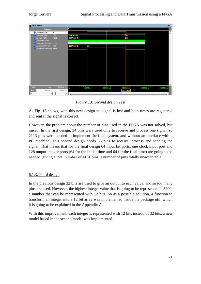
Figure 13: Second design Test
As Fig. 13 shows, with this new design no signal is lost and both times are registered and sent if the signal is correct.
However, the problem about the number of pins used in the FPGA was not solved, but raised. In the first design, 34 pins were used only to receive and process one signal, so 2113 pins were needed to implement the final system, and without an interface with a PC machine. This second design needs 66 pins to receive, process and sending the signal. That means that for the final design 64 input bit ports, one clock input port and 128 output integer ports (64 for the initial time and 64 for the final time) are going to be needed, giving a total number of 4161 pins, a number of pins totally unacceptable.
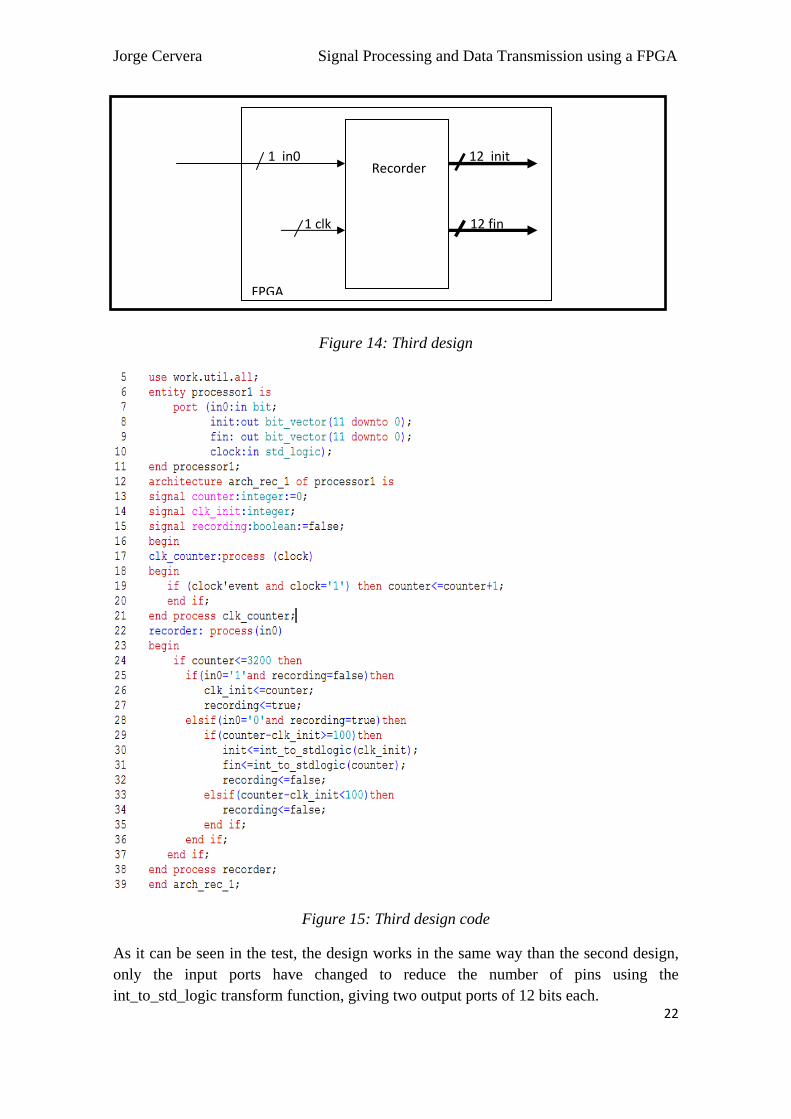
6.1.3. Third design
In the previous design 32 bits are used to give an output to each value, and so too many pins are used. However, the highest integer value that is going to be represented is 3200, a number that can be represented with 12 bits. So as a possible solution, a function to transform an integer into a 12 bit array was implemented inside the package util, which it is going to be explained in the Appendix A.
With this improvement, each integer is represented with 12 bits instead of 32 bits, a new model based in the second model was implemented.
Jorge Cervera Signal Processing and Data Transmission using a FPGA
22
Figure 14: Third design
Figure 15: Third design code
As it can be seen in the test, the design works in the same way than the second design, only the input ports have changed to reduce the number of pins using the int_to_std_logic transform function, giving two output ports of 12 bits each.
1 in0 12 init
1 clk 12 fin
FPGA
Recorder

Jorge Cervera Signal Processing and Data Transmission using a FPGA
23
Figure 16: Third design test
This was an improvement to the design, but not a solution, because in this third design 26 pins are utilized with just one input signal, so if 64 signals were going to be processed, 1601 pins would have to be utilized, still a very high number.
6.1.4. Fourth Design
After this third design I thought that it could not be improved, as two integer values had to be sent to the PC machine, and after implementing the int_to_std_logic transform function to make the integer bit representation as small as possible I thought that nothing else could be done. But then I realized that according to the project requirements, the input signals had to be received and processed in parallel, but then they could be stored in a data matrix and after sent to the PC machine sequentially, through a bit port. As the maximum time of recording is 3.2 ms, and a signal has to last a minimum time lapse of 100 µs, that gives a maximum of 32 measures for the initial time of the signal and 32 measures for the final time of the signal in the worst case, one valid signal every 100 µs.
Figure 17: Fourth design
1 in0
12 out0
1 clock
FPGA
Recorder
Jorge Cervera Signal Processing and Data Transmission using a FPGA
24
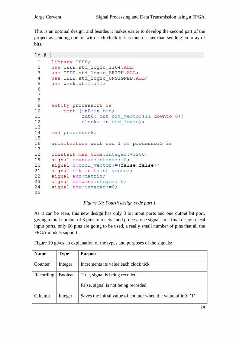
This is an optimal design, and besides it makes easier to develop the second part of the project as sending one bit with each clock tick is much easier than sending an array of bits.
Figure 18: Fourth design code part 1
As it can be seen, this new design has only 3 bit input ports and one output bit port, giving a total number of 3 pins to receive and process one signal. In a final design of 64 input ports, only 66 pins are going to be used, a really small number of pins that all the FPGA models support.
Figure 19 gives an explanation of the types and purposes of the signals:
Name Type Purpose
Counter Integer Increments its value each clock tick
Recording Boolean True, signal is being recoded.
False, signal is not being recorded.
Clk_init Integer Saves the initial value of counter when the value of in0=’1’

Jorge Cervera Signal Processing and Data Transmission using a FPGA
25
Aux Matrix Saves the value of the initial and ending times of a valid signal. The value of the rows indicates the number of the port.
Column Integer Value of the columns of the matrix
Aux1 Bit vector
Saves the value of the bit vector that is being sent to the PC machine
Row Integer Value of the rows of the matrix
Figure 19: Fourth design Table of signals
Figure 20: Fourth design code part 2
The basic processes keep doing the same functions than in the previous design, but now the values of the initial time and of the final time of a valid signal are stored in the signal aux after being converted in an 11 bit vector.

Jorge Cervera Signal Processing and Data Transmission using a FPGA
26
Figure 21: Fourth design code part 3
This new process is the one that makes possible to send all the information bit by bit. It is activated with each clock tick after the maximum time of recording has been exceeded, and it begins to read the matrix aux, keeping the value in the signal aux1 that is sent bit by bit through the port out0, beginning from the msb to give the exact values of initial and final time. These values should be processed in the PC machine to reconvert them into integer values for further use.
Figure 22: Fourth designn test

Jorge Cervera Signal Processing and Data Transmission using a FPGA
27
6.1.5. Fifth design
The fifth and final design contains the implementation of the design using two input ports instead of one. Some user-defined data are utilized; they are implemented in the package util, which is widely explained in the Appendix A.
Figure 23: Fifth design
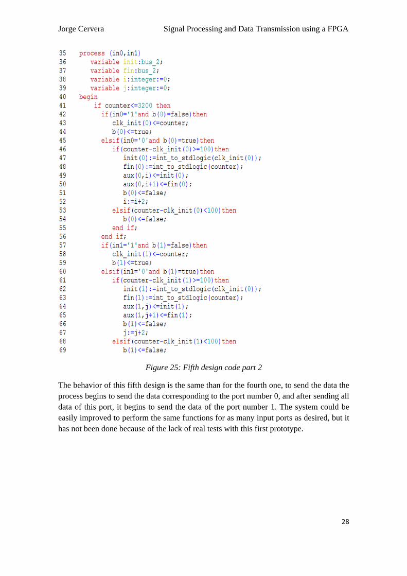
Figure 24: Fifth design code part 1
The basic functioning is the same than in the previous design, only one process changes a little bit, including a second input signal in the sensitivity list, and some signals changes to store the values corresponding to the second signal data, as it can be seen in Figures 24 and 25.
1 in0
1 in1
12 out0
1 clock
FPGA
Recorder
Jorge Cervera Signal Processing and Data Transmission using a FPGA
28
Figure 25: Fifth design code part 2
The behavior of this fifth design is the same than for the fourth one, to send the data the process begins to send the data corresponding to the port number 0, and after sending all data of this port, it begins to send the data of the port number 1. The system could be easily improved to perform the same functions for as many input ports as desired, but it has not been done because of the lack of real tests with this first prototype.

Jorge Cervera Signal Processing and Data Transmission using a FPGA
29
Figure 16: Fifth design test
Figure 26 shows how two valid signals are recorded (one in each input signal port) and then sent bit by bit through the same output port.
6.2. Second Part: Designing of a system capable of interact with a PC machine:
In this second part of the project, a design capable of interact with a PC machine is developed. The system is based on a interface through the RS-232 port of the PC and the machine. This part is also divided into three sub-parts, to make the developing process easier and more understandable. First, a brief explanation of the hardware needed will be given. In the second part, a transmitter design will be explained implemented and tested. The device is capable of sending data bit by bit. In the third part, a design capable of receiving data from the pc is implemented. This device is needed because the PC must be able to give some simple orders to the FPGA, such start-record, or stop-record. Both devices use an "asynchronous" protocol. That means that no clock signal is transmitted along the data. The receiver has to have a way to "time" itself to the incoming data bits. In the case of RS-232, that's done this way:
1. Both side of the cable agree in advance on the communication parameters (speed, format...). That's done manually before communication starts.
2. The transmitter sends a "1" when and as long as the line is idle. 3. The transmitter sends a "start" (a "0") before each byte transmitted, so that the
receiver can figure out that data is coming. 4. After the "start", data comes in the agreed speed and format, so the receiver can
interpret it. 5. The transmitter sends a "stop" (a "1") after each data byte.

Jorge Cervera Signal Processing and Data Transmission using a FPGA
30
6.2.1. Hardware:
RS-232 (Recommended Standard 232) is a standard for serial binary data signals connecting between a DTE (Data terminal equipment) and a DCE (Data Circuit-terminating Equipment). It is commonly used in computer serial ports.
An RS-232 interface has the following characteristics:
• Uses a 9 pins connector "DB-9". • Allows bidirectional full-duplex communication (the PC can send and receive
data at the same time). • Can communicate at a maximum speed of roughly 10KBytes/s.
Figure 27: Male RS-232 plug
It has 9 pins, but the 3 important ones are:
• pin 2: RxD (receive data). • pin 3: TxD (transmit data). • pin 5: GND (ground).
Using just 3 wires, you can send and receive data.
To connect the FPGA with a regular PC a j is needed.
Figure 28: Female to female DB-9 cable
Jorge Cervera Signal Processing and Data Transmission using a FPGA
31
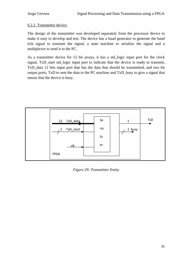
6.2.2. Transmitter device:
The design of the transmitter was developed separately from the processor device to make it easy to develop and test. The device has a baud generator to generate the baud tick signal to transmit the signal, a state machine to serialize the signal and a multiplexor to send it to the PC.
As a transmitter device for 12 bit arrays, it has a std_logic input port for the clock signal, TxD_start std_logic input port to indicate that the device is ready to transmit, TxD_data 12 bits input port that has the data that should be transmitted, and two bit output ports, TxD to sent the data to the PC machine and TxD_busy to give a signal that means that the device is busy.
Figure 29: Transmitter Entity
TxD
12 TxD_data 1
1 TxD_start 1 busy
clk
FPGA
Se
ria
liz
er

Jorge Cervera Signal Processing and Data Transmission using a FPGA
32
Figure 30: Transmitter Entity,Constants and Signals
Name Type Purpose
BaudGeneratorACC Std_logic_vector Baud generator accuracy, changes its value when the device is busy
State Std_logic_vector Points to the state of the device
TxD_ready Std_logic ‘1’ means the device is ready to transmit, ‘0’ means it is busy
TxD_dataReg Std_logic_vector It is used to store the data that is being sent to the PC
BaudTick Std_logic Signal to point each baud tick (speed)
Muxbit Std_logic Aims to the beginning of a new data

Jorge Cervera Signal Processing and Data Transmission using a FPGA
33
busy Std_logic ‘1’ the device is busy, ‘0’ the device is ready to transmit
Figure 31: Transmitter Table of signals
Baud generator: As a first step I thought about the speed that is desired for the transmission. The speed is specified in baud, i.e. how many bits-per-seconds can be sent. For example, 1000 bauds would mean 1000 bits-per-seconds, or that each bit lasts one millisecond.
Common implementations of the RS-232 interface (like the one used in PCs) don't allow just any speed to be used. One of the following “standard” speeds has to be selected:
• 200 bauds. • 9600 bauds. • 38400 bauds. • 115200 bauds.
The device must be as fast as possible, and as RS-232 are not very fast actually, for instance, at 115200 bauds, each bit lasts (1/115200) = 8.7µs. If you transmit 12-bits data, that lasts 12 x 8.7µs = 104.4µs. But each byte requires an extra start and stop bit, so you actually need 14 x 8.7µs = 121.8µs. So the highest value for the speed is selected to provide an acceptable time transfer value.
Here's a design with a 25MHz clock and a 16 bits accumulator. The design is parameterized, so easy to customize.
Figure 32: Transmitter Baud Generator
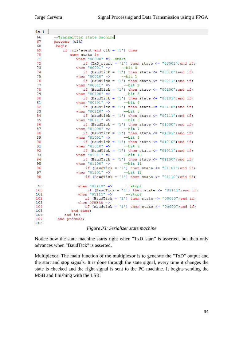
State machine: The first state machine takes a 12-bits data signal, and serializes it starting when the TxD_start signal is asserted. The "busy" signal is asserted while a transmission occurs. The "TxD_start" signal is ignored during that time. The RS-232 parameters used are fixed: 12-bits data, 2 stop bits, no-parity. The state machine is activated every clock tick.
Jorge Cervera Signal Processing and Data Transmission using a FPGA
34
Figure 33: Serializer state machine
Notice how the state machine starts right when "TxD_start" is asserted, but then only advances when "BaudTick" is asserted.
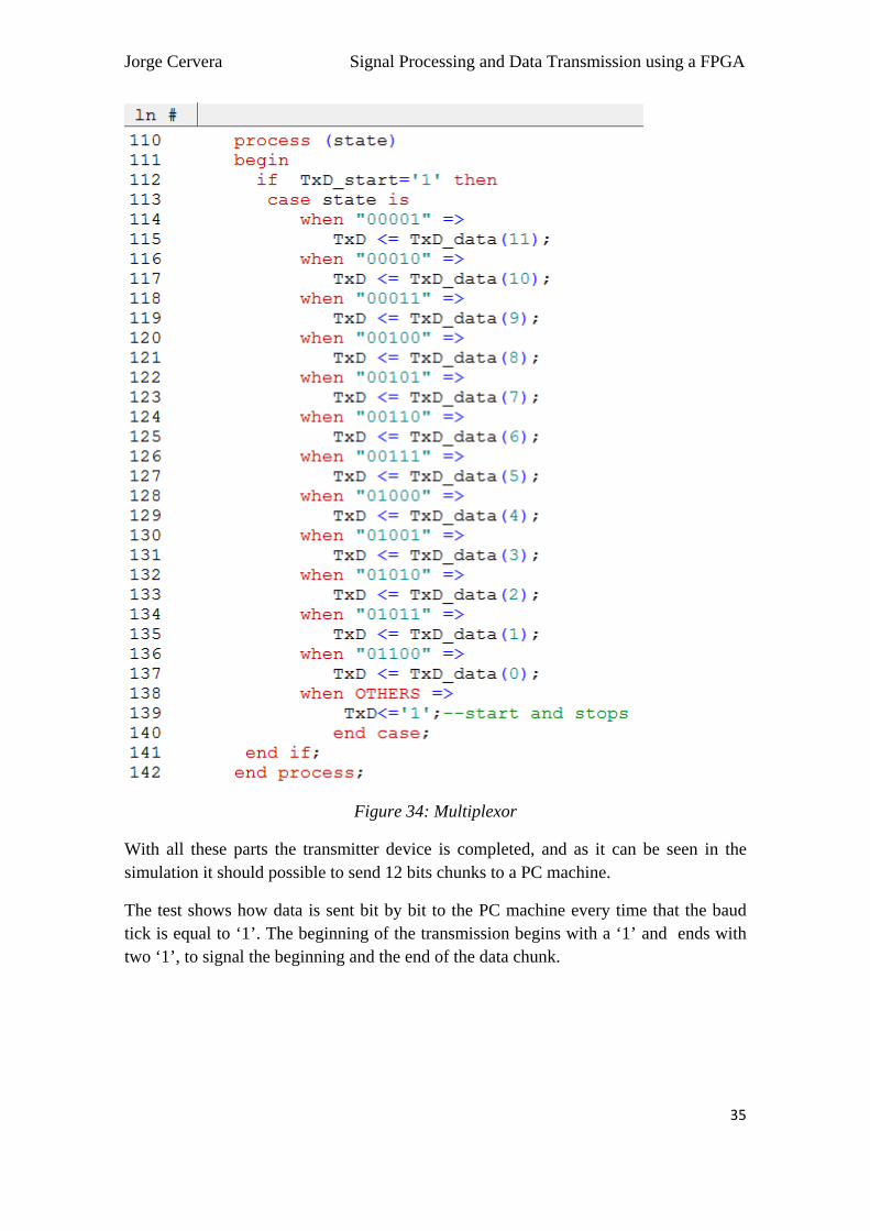
Multiplexor: The main function of the multiplexor is to generate the "TxD" output and the start and stop signals. It is done through the state signal, every time it changes the state is checked and the right signal is sent to the PC machine. It begins sending the MSB and finishing with the LSB.
Jorge Cervera Signal Processing and Data Transmission using a FPGA
35
Figure 34: Multiplexor
With all these parts the transmitter device is completed, and as it can be seen in the simulation it should possible to send 12 bits chunks to a PC machine.
The test shows how data is sent bit by bit to the PC machine every time that the baud tick is equal to ‘1’. The beginning of the transmission begins with a ‘1’ and ends with two ‘1’, to signal the beginning and the end of the data chunk.

Jorge Cervera Signal Processing and Data Transmission using a FPGA
36
Figure 35: Transmitter test
6.2.3. Receiver device:
The design of the receiver was developed separately from the processor device to make it easy to develop and test. A baud generator like in the transmitter device is used.
First, the incoming "RxD" signal has no relationship with our clock. Two D-flipflops are used to oversample it, and synchronize it to our clock. The data are filtered, so that short spikes on the RxD line aren't mistaken with start bits. Then a state machine allows to go through each bit received, once a "start" is detected, and finally a shift register collects the data bits as they come.
As a receiver, the device has one input std_logic port for the clock signal, the RxD iniput port that receives the data sent by the PC, RxD_data_ready that is activated when the data are synchronized and ready to be read, and RxD_endofpacket that indicates when a packet has been read.

Jorge Cervera Signal Processing and Data Transmission using a FPGA
37
Figure 36: Receiver Entity
Figure 37: Receiver Entity, Constants and Signals
Name Type Purpose
Baud8GeneratorAcc Std_logic_vector Baud generator accuracy, changes its value when the device is busy
Baud8Tick Std_logic Signal to point each baud tick (speed)
RxD_sync_inv Std_logic_vector Signal used to synchronize (Flip- Flop)
RxD
1 8
data
clk 1 data_ready
FPGA
De
se
ria
li
zer

Jorge Cervera Signal Processing and Data Transmission using a FPGA
38
RxD_cnt_inv Std_logic_vector Signal used to synchronize, it is used as a counter
RxD_bit_inv Std_logic_vector Signal that changes the state of the device
State Std_logic_vector Points to the state of the device Bit_spacing Std_logic_vector Signal used for “timing” when receiving data.
Next_bit Std_logic Indicates when a next bit can be received
RxD_data_error Std_logic Indicates when a there is an error, and no transmission is made
RxD_d Std_logic_vector It is used to store the data that is being received by the FPGA
Index Integer Points to the position when the data is going to be saved
Figure 38: Receiver Table of Signals
Baud Generator: The baud generator follows the same process than for the transmitter machine, only the constant BaudGeneratorInc has changed because the timing of receiving signals is higher than for transmitting, and after reading some papers it has been set that this is the most adapted value.
Figure 39: Receiver Baud Generator
D- Flip-Flops: The flip-flops are implemented by the RxD_sync_inv, signal. The value of the LSB bit of the signal and set it as the MSB, and then the value of the RxD port is added. RxD is inverted, so that the idle becomes "0", to prevent a phantom character to be received at startup

Jorge Cervera Signal Processing and Data Transmission using a FPGA
39
Figure 40: D-Flip-Flop
The data are filtered, so that short spikes on the RxD line aren't mistaken with start bits.
Figure 41: Received data filter
State machine: The state machine goes through different states to point to the position of the array signal where the data must be writen, once a start is detected. Notice that a "next_bit" signal is used to go from bit to bit.

Jorge Cervera Signal Processing and Data Transmission using a FPGA
40
Figure 42: Receiver state machine
Shift register: The shift register evaluates which are the conditions to write, and if so, it sends the information through the RxD_d signal and eventually it sends the complete 8 bit array to the output port. The signal is only registered if the input signal is a “0” or a “1”.
Figure 43: Receiver Shift register

Jorge Cervera Signal Processing and Data Transmission using a FPGA
41
With all these parts the transmitter device is completed, and as it can be seen in the simulation it should possible to receive 8 bit chunks from a PC machine.
Figure 44: Receiver Test
6.3. Third Part: Assembling of the three components: Once every component has been developed and simulated, it is time to assemble the three of them. VHDL allows a very easy way to link components, so it has not been very difficult to do it. Just a few modifications have been needed to make all the components to work together.

Jorge Cervera Signal Processing and Data Transmission using a FPGA
42
Figure 45: Final design
The processor is the main component, and the receiver and the transmitter work as components of it, so the main difference with the previous version of the processor is that some ports have been added to it to make possible to connect it with the other two components. The port that took the output signal (out0) has been substituted by the PC_TxD_data port, that has the same function.
Figure 46: Processor entity
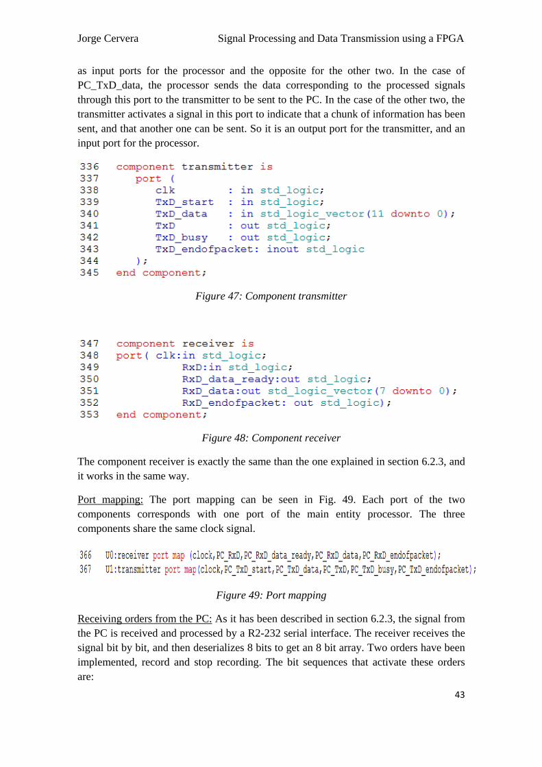
The transmitter and the receiver are declared as components of the main entity processor. The PC_TxD_data, TxD_start and the PC_TxD_endofpacket ports of the processor are declared as inout, as the first work as output ports for the transmitter, and
RxD
In0 1
1 8 data 12 data 1 TxD
1 ready 1 start 1busy
Clk clk
Clk
FPGA
Transmitter
Receiver
Processor
Jorge Cervera Signal Processing and Data Transmission using a FPGA
43
as input ports for the processor and the opposite for the other two. In the case of PC_TxD_data, the processor sends the data corresponding to the processed signals through this port to the transmitter to be sent to the PC. In the case of the other two, the transmitter activates a signal in this port to indicate that a chunk of information has been sent, and that another one can be sent. So it is an output port for the transmitter, and an input port for the processor.
Figure 47: Component transmitter
Figure 48: Component receiver
The component receiver is exactly the same than the one explained in section 6.2.3, and it works in the same way.
Port mapping: The port mapping can be seen in Fig. 49. Each port of the two components corresponds with one port of the main entity processor. The three components share the same clock signal.
Figure 49: Port mapping
Receiving orders from the PC: As it has been described in section 6.2.3, the signal from the PC is received and processed by a R2-232 serial interface. The receiver receives the signal bit by bit, and then deserializes 8 bits to get an 8 bit array. Two orders have been implemented, record and stop recording. The bit sequences that activate these orders are:

Jorge Cervera Signal Processing and Data Transmission using a FPGA
44
• 10000001 – Record.
• 10000010 – Stop recording.
When the system receives the Record signal sequence, it begins to receive the signals and processing them. The counter signal is initialized and the process that measures the timing of the signals begins to work.
Figure 50: Counter signal with PC start order
Figure 51: Processing signals with PC start order

Jorge Cervera Signal Processing and Data Transmission using a FPGA
45
When the system receives the Stop recording signal sequence, it stops recording and sends all the information to the PC, the same action that the system takes when a complete recording sequence has been complete.
Figure 52: Stop signal PC order
Watching at the code, some differences between the code in the fifth design of the processor and the final design can be seen, and it is not only the “if” clause corresponding to the PC signal to stop. In the fifth design, one value of the aux signal was sent with each clock tick. But this is too fast for our transmitter that works sending one bit each baud tick, so the variable has to keep the same value until all the data bits plus the two stop bits are sent to the PC. This is made through the PC_TxD_endofpacket port, that keeps a value of ‘0’ until the last stop bit has been sent, taking the value of ‘1’ and letting the process to take other data value to send to the PC machine. Besides, the port PC_TxD_Start is set to ‘1’ to make the transmission of data begin.
The final design requires the following resources:
• 3444 logic elements
• 30 pins
• 0 memory bits

Jorge Cervera Signal Processing and Data Transmission using a FPGA
46
The number of pins is still very low, for a 64 input port device we will need 92 pins, a really small number. The device needs 3444 logic elements. More logic elements will be used with a more complex device, however it is not a really high number for the FPGA devices that can be found in the market. For instance, a Cyclone device from Altera has about 250 pins and 4.000 logic elements, and this is the most cheap and simple device from Altera.
6.4. Final Test:
Now it is time to test the whole application, testing each one of the functions.
Figure 53 shows how the counter signal does not begin to increase until the code for recording has been received by the FPGA, and no other processes are activated.
Figure 53: Final Test, Record code received
In Fig.54, we can see how an impulse has been received in the in0 port, but as it lasts less than 100 µs, it is rejected and the values of the initial and the final time of the signal are not recorded in aux(0,0) and aux(0,1).
Jorge Cervera Signal Processing and Data Transmission using a FPGA
47
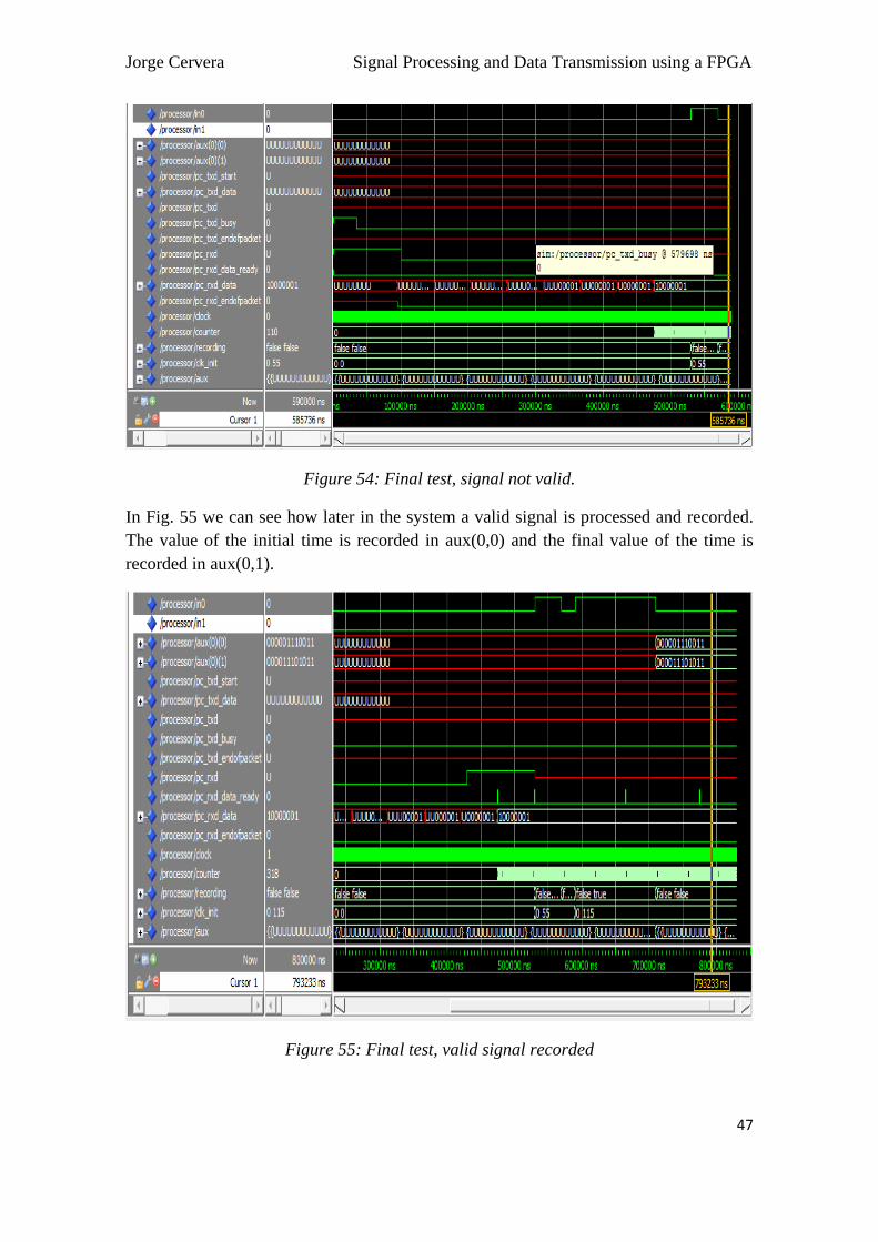
Figure 54: Final test, signal not valid.
In Fig. 55 we can see how later in the system a valid signal is processed and recorded. The value of the initial time is recorded in aux(0,0) and the final value of the time is recorded in aux(0,1).
Figure 55: Final test, valid signal recorded

Jorge Cervera Signal Processing and Data Transmission using a FPGA
48
Now in case of another valid signal, the values of the initial and final time of the signal would be recorded in aux (0,2) and aux (0,3). The same process using the same algorithm is used for the signals that come from the input port in1, so no further tests are going to be done of this algorithm because it is clear that it is working.
Now the stop record signal is given, so the system must start to transmit the recorded data. As it can be seen in Fig.56, as soon as the complete code for the order Stop recording is received, the counter signal stops, the port pc_txd_start is activated and the transmission starts. The complete sequence of transmitted bits can be seen in the pc_txd port and in the pc_txd_data port.
Figure 56: Final test, Transmission finished.
Note than the end of the transmission of each chunk of data is denoted with a ‘1’ in the pc_txd_endofpacket port.
7. Conclusions Finally a system capable of processing signals coming from an external source, receiving simple orders from a PC machine and transmit the processed data has been developed. The purpose of this work is to serve as a prototype for future development and improvements. As a first approach it has some advantages and many drawbacks.
Jorge Cervera Signal Processing and Data Transmission using a FPGA
49
7.1. Advantages:
All the project requirements are fulfilled. The system is capable of receiving a digital signal and processing it, finding if it is a valid signal or not. The algorithms used to implement the processing function are quite easy to understand, and they can be easily improved to receive as many signals as desired.
The receiver and transmitter components provide serial asynchronous transmission of data from and to a PC machine.
7.2. Drawbacks:
The algorithm used to process the signal works and can be used to process more signals simply doing some copy-paste job and adjusting three parameters. However this is not a good way of programming, as it takes to a lot of “rubbish code” and to the consumption of many unneeded resources.
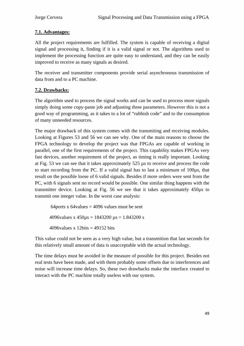
The major drawback of this system comes with the transmiting and receiving modules. Looking at Figures 53 and 56 we can see why. One of the main reasons to choose the FPGA technology to develop the project was that FPGAs are capable of working in parallel, one of the first requirements of the project. This capability makes FPGAs very fast devices, another requirement of the project, as timing is really important. Looking at Fig. 53 we can see that it takes approximately 525 µs to receive and process the code to start recording from the PC. If a valid signal has to last a minimum of 100µs, that result on the possible loose of 6 valid signals. Besides if more orders were sent from the PC, with 6 signals sent no record would be possible. One similar thing happens with the transmitter device. Looking at Fig. 56 we see that it takes approximately 450µs to transmit one integer value. In the worst case analysis:
64ports x 64values = 4096 values must be sent
4096values x 450µs = 1843200 µs = 1.843200 s
4096values x 12bits = 49152 bits
This value could not be seen as a very high value, but a transmition that last seconds for this relatively small amount of data is unacceptable with the actual technology.
The time delays must be avoided in the measure of possible for this project. Besides not real tests have been made, and with them probably some offsets due to interferences and noise will increase time delays. So, these two drawbacks make the interface created to interact with the PC machine totally useless with our system.

Jorge Cervera Signal Processing and Data Transmission using a FPGA
50
7.3 Future Work:
This section has only the purpose of giving a guide of what I would do if I could continue working with the project, and to help other people that maybe will continue with it.
As I said before, the algorithm to process the signal works, but it is not ”good programming”. One algorithm could manage all the processing work for all the ports, not one algorithm per each port. This could be make through some kind of loop, but taking count of the increased logic units that will be needed.
My work with the interface with the PC has proved to be completely useless due to time delays. Serial and asynchronous communication is the easiest way to implement an interface, and as I am not an expert in VHDL, I took this as a first option. I knew that it would be slow, but I hoped that the time delays would not be significant for the system. Unfortunately tests have proved that this kind of interface is completely useless for the project. For future improvements, a synchronous and parallel interface should be investigated and implemented if possible. Synchronous transmissions take time at the beginning during synchronization, but then the transmission is faster than if it is asynchronous. And of course parallel transmission are much faster that serial, and FPGAs support this kind of transmission as well as PC machines.
And as a final recommendation, real tests with the FPGA should be made. It is easy to simulate a design and to make it work “virtually”, but in reality things are different. You will never know if your design works only simulating tests.
8. References
1. http://en.wikipedia.org/wiki/FPGA, last access 4th April 2008
2. http://en.wikipedia.org/wiki/VHDL, last access 7th April 2008
3. http://en.wikipedia.org/wiki/Verilog, last access 7th April 2008
4. http://www.altera.com, last access 15th April 2008
5. http://www.xilinx.com, last access 10th April 2008
6. http://www.fpga4fun.com last access 28th May 2008
7. http://www.model.com, last access 12th April 2008
8. “Digital Design Principles and Practices4th Edition”, John F. Wakerly, Prentice Hall.
9. “VHDL 3rd Edition”, Douglas Perry, McGraw-Hill.

Jorge Cervera Signal Processing and Data Transmission using a FPGA
51
10. John V. Oldfield and Richard C. Dorf “Field Programmable Gate Arrays-Reconfigurable Logic for Rapid Prototyping and Implementation of Digital Systems”, Wiley Interscience, 1995.
11. Lennart Lindh, Tommy Klevin. Progammerbara kretsar, ”Utveckling av inbyggda system”.
12. Richard A. Blum, “An Electronic System For Extracellular Neural Stimulation And Recording”, Georgia Institute of Technology August 2007.
13. Tobias Nyberg, Akiyoshi Shimada, Keiichi Torimitsu, “Ion conducting polymer microelectrodes for interfacing with neural networks”, NTT Basic Research Laboratories, NTT Corporation, Atsugi, Kanagawa 243-0198, Japan, 9 August 2006.
14. Yasuhiko Jimbo, Nahoko Kasai, Keiichi Torimitsu, Takashi Tateno, and Hugh P. C. Robinson, “A System for MEA-Based Multisite Stimulation”, IEEE Transactions on Biomedical Engineering, Vol.50, No.2, February 2003.
15. Douglas E. Ott and Thomas J. Wilderotter, "A Designer's Guide to VHDL Synthesis", Kluwer Academic Publishers.
16. David Pellerin and Douglas Taylor, "VHDL Made Easy", Prentice Hall.
17. Charles E. Roth, Jr., "Digital System Design Using VHDL" , PWS Publishing Company.

Jorge Cervera Signal Processing and Data Transmission using a FPGA
52
Appendix A: The util package:
The util package is a package that contains some user defined types and constants and the function used to transform an integer into a 12 bit array. It is really simple and useful. All the future conversion functions and user defined types should be placed in this package.
The only constant defined is max_ports, that is equal to the maximum number of input signal ports of the processor minus 1, due to 0.
The following are the used defined types:
Name Type
Bool_vector array (max_ports downto 0) of boolean
Int_vector array(max_ports downto 0)of integer range 0 to 3200
Bus_2 array(max_ports downto 0) of std_logic_vector(11 downto 0)
Bus_6 array (5 downto 0)of bit_vector(11 downto 0)
matrix array (max_ports downto 0,64 downto 0)of std_logic_vector(11 downto 0);
Figure 57: Package util user defined types

Jorge Cervera Signal Processing and Data Transmission using a FPGA
53
Figure 58: Package util code
Appendix B: Time Planning
I had a very clear idea of how to divide the project from the beginning. One was a processor, the other one was about creating an interface with the PC, and the last part was to assemble all the parts. I had to spent a lot of time learning VHDL after choosing it as the programming language of the projcec, as it was a new programming language for me.
After that, programming the three parts took most of my time, being the problems with the resources when working with the processor the main problem, and the problems of synchronizing were a problem too when assembling. During all the time of developing, I wrote this paper, so no important details were forgotten.

Jorge Cervera Signal Processing and Data Transmission using a FPGA
54
Figure 59: Time planning