silicon-integrated short-wavelength hybrid- cavity … · silicon-integrated short-wavelength...
TRANSCRIPT
Silicon-integrated short-wavelength hybrid-cavity VCSEL
Emanuel P. Haglund,1,4,* Sulakshna Kumari,2,3,4 Petter Westbergh,1 Johan S. Gustavsson,1 Gunther Roelkens,2,3 Roel Baets,2,3 and Anders Larsson1
1Photonics Laboratory, Department of Microtechnology and Nanoscience, Chalmers University of Technology, SE-41296 Göteborg, Sweden
2Photonics Research Group, INTEC Department, Ghent University–IMEC, Belgium 3Center for Nano-and Biophotonics, Ghent University, Belgium
4contributed equally *[email protected]
Abstract: We demonstrate a short-wavelength hybrid-cavity vertical-cavity surface-emitting laser (VCSEL) heterogeneously integrated on silicon. A GaAs-based “half-VCSEL” has been attached to a dielectric distributed Bragg reflector (DBR) on a silicon wafer using ultra-thin divinylsiloxane-bis-benzocyclobutene (DVS-BCB) adhesive bonding, thereby creating a cavity with the standing-wave optical field extending over the silicon- and GaAs-based parts of the cavity. A 9 µm oxide aperture diameter VCSEL with a threshold current of 1.2 mA produces 1.6 mW optical output power at 6.0 mA bias current with a wavelength of ~845 nm.
©2015 Optical Society of America
OCIS codes: (250.5300) Photonic integrated circuits; (250.5960) Semiconductor lasers; (250.7260) Vertical cavity surface emitting lasers.
References and links 1. A. Z. Subramanian, P. Neutens, A. Dhakal, R. Jansen, T. Claes, X. Rottenberg, F. Peyskens, S. Selvaraja, P.
Helin, B. DuBois, K. Leyssens, S. Severi, P. Deshpande, R. Baets, and P. Van Dorpe, “Low-loss singlemode PECVD silicon nitride photonic wire waveguides for 532–900 nm wavelength window fabricated within a CMOS pilot line,” IEEE Photonics J. 5(6), 2202809 (2013).
2. K. Takaki, N. Iwa, K. Hiraiwa, S. Imai, H. Shimizu, T. Kageyama, Y. Kawakita, N. Tsukiji, and A. Kasukawa, “A recorded 62% PCE and low series and thermal resistance VCSEL with a double intra-cavity structure,” in Proceedings of IEEE International Semiconductor Laser Conference (IEEE, 2008), post deadline paper PDP1.
3. E. Haglund, P. Westbergh, J. S. Gustavsson, E. P. Haglund, A. Larsson, M. Geen, and A. Joel, “30 GHz bandwidth 850 nm VCSEL with sub-100 fJ/bit energy dissipation at 25–50 Gbit/s,” Electron. Lett. 51(14), 1096–1098 (2015).
4. D. M. Kuchta, A. V. Rylyakov, F. E. Doany, C. L. Schow, J. E. Proesel, C. W. Baks, P. Westbergh, J. S. Gustavsson, and A. Larsson, “A 71-Gb/s NRZ modulated 850-nm VCSEL-based optical link,” IEEE Photonics Technol. Lett. 27(6), 577–580 (2015).
5. P. Moser, J. A. Lott, P. Wolf, G. Larisch, H. Li, N. N. Ledentsov, and D. Bimberg, “56 fJ dissipated energy per bit of oxide-confined 850 nm VCSELs operating at 25 Gbit/s,” Electron. Lett. 48(20), 1292–1294 (2012).
6. Y. Tsunemi, N. Yokota, S. Majima, K. Ikeda, T. Katayama, and H. Kawaguchi, “1.55-μm VCSEL with polarization-independent HCG mirror on SOI,” Opt. Express 21(23), 28685–28692 (2013).
7. J. Ferrara, W. Yang, L. Zhu, P. Qiao, and C. J. Chang-Hasnain, “Heterogeneously integrated long-wavelength VCSEL using silicon high contrast grating on an SOI substrate,” Opt. Express 23(3), 2512–2523 (2015).
8. R. Wang, D. Sanchez, and G. Roelkens, “Design of a high contrast grating GaSb-based VCSEL integrated on silicon-on-insulator,” in Proceedings of IEEE Photonics Conference (IEEE, 2013), pp. 91–92.
9. D. A. Louderback, G. W. Pickrell, H. C. Lin, M. A. Fish, J. J. Hindi, and P. S. Guilfoyle, “VCSELs with monolithic coupling to internal horizontal waveguides using integrated diffraction gratings,” Electron. Lett. 40(17), 1064–1065 (2004).
10. S. Keyvaninia, M. Muneeb, S. Stanković, P. J. Van Veldhoven, D. Van Thourhout, and G. Roelkens, “Ultra-thin DVS-BCB adhesive bonding of III-V wafers, dies and multiple dies to a patterned silicon-on-insulator substrate,” Opt. Mater. Express 3(1), 35–46 (2013).
11. P. Westbergh, J. S. Gustavsson, B. Kögel, A. Haglund, and A. Larsson, “Impact of photon lifetime on high-speed VCSEL performance,” IEEE J. Sel. Top. Quantum Electron. 17(6), 1603–1613 (2011).
12. V. Karagodsky, B. Pesala, C. Chase, W. Hofmann, F. Koyama, and C. J. Chang-Hasnain, “Monolithically integrated multi-wavelength VCSEL arrays using high-contrast gratings,” Opt. Express 18(2), 694–699 (2010).
13. I. S. Chung and J. Mørk, “Silicon-photonics light source realized by III-V/Si-grating-mirror laser,” Appl. Phys. Lett. 97(15), 151113 (2010).
#251697 Received 12 Oct 2015; revised 11 Dec 2015; accepted 11 Dec 2015; published 21 Dec 2015 © 2015 OSA 28 Dec 2015 | Vol. 23, No. 26 | DOI:10.1364/OE.23.033634 | OPTICS EXPRESS 33634
14. G. C. Park, W. Xue, E. Semenova, K. Yvind, J. Mørk, and I. Chung, “III-V/SOI Vertical cavity laser with in-plane output into a Si waveguide,” in Optical Fiber Communication Conference, OSA Technical Digest (online) (Optical Society of America, 2015), paper W2A.17.
15. S. Kumari, J. S. Gustavsson, R. Wang, E. P. Haglund, P. Westbergh, D. Sanchez, E. Haglund, Å. Haglund, J. Bengtsson, N. Le Thomas, G. Roelkens, A. Larsson, and R. Baets, “Integration of GaAs-based VCSEL array on SiN platform with HCG reflectors for WDM applications,” Proc. SPIE 9372, 93720U (2015).
16. G. C. DeSalvo, A. Bozada Christopher, J. L. Ebel, D. C. Look, J. P. Barrette, C. L. A. Cerny, R. W. Dettmer, J. K. Gillespie, C. K. Havasy, T. J. Jenkins, K. Nakano, C. I. Pettiford, T. K. Quach, J. S. Sewell, and G. D. Via, “Wet chemical digital etching of GaAs at room temperature,” J. Electrochem. Soc. 143(11), 3652–3656 (1996).
17. W. Kern, “The evolution of silicon wafer cleaning technology,” J. Electrochem. Soc. 137(6), 1887–1892 (1990). 18. E. Haglund, P. Westbergh, J. S. Gustavsson, E. P. Haglund, and A. Larsson, “High-speed VCSELs with strong
confinement of optical fields and carriers,” J. Lightwave Technol. (posted 21 July 2015, in press). 19. A. N. Al-Omari and K. L. Lear, “VCSELs with a self-aligned contact and copper-plated heatsink,” IEEE
Photonics Technol. Lett. 17(9), 1767–1769 (2005). 20. E. P. Haglund, S. Kumari, P. Westbergh, J. S. Gustavsson, R. G. Baets, G. Roelkens, and A. Larsson, “20 Gb/s
modulation of silicon-integrated short-wavelength hybrid-cavity VCSELs,” IEEE Photon. Technol. Lett. (to be published).
1. Introduction
The development of photonic integrated circuits (PICs) on a silicon nitride waveguide platform [1] would benefit applications using light in the visible and near infrared (where silicon nitride is transparent, in contrast to Si), such as life sciences and short wavelength optical interconnects. Such PICs need an integrated, low current and high efficiency light source. For optical interconnects, the light source should also be capable of high speed operation. The GaAs-based vertical-cavity surface-emitting laser (VCSEL) has demonstrated power conversion efficiencies exceeding 60% [2], modulation bandwidths up to 30 GHz [3], data rates exceeding 70 Gb/s [4], and energy dissipation less than 100 fJ/bit at data rates up to 50 Gb/s [3,5] with drive currents of only a few milliamperes. Therefore, the GaAs-based VCSEL is attractive as a light source on the silicon nitride waveguide platform for applications requiring wavelengths in the range ~650–1100 nm.
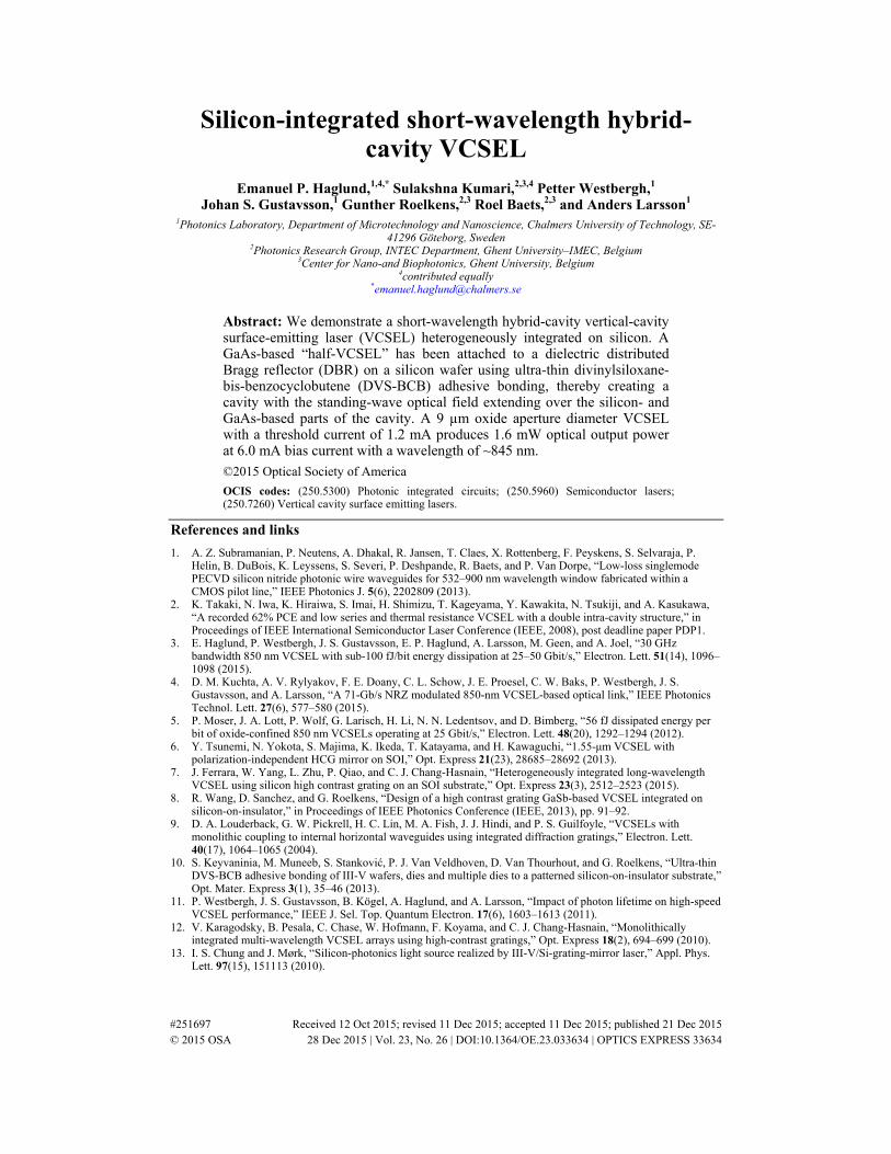
An approach for VCSEL integration that lends itself to wafer-level processing is heterogeneous integration, where a III-V semiconductor epitaxial structure containing a distributed Bragg reflector (DBR) and an active region (“half-VCSEL”) is attached to an optical reflector on the Si wafer. This forms a hybrid cavity where the standing-wave optical field extends over the III-V and the Si-integrated parts [6–8]. One example is illustrated in Fig. 1 where the reflector on Si is a dielectric DBR and a weak diffraction grating in the hybrid cavity is used to tap off power to an in-plane silicon nitride waveguide. A similar technology has previously been explored for an all III-V semiconductor based design [9].
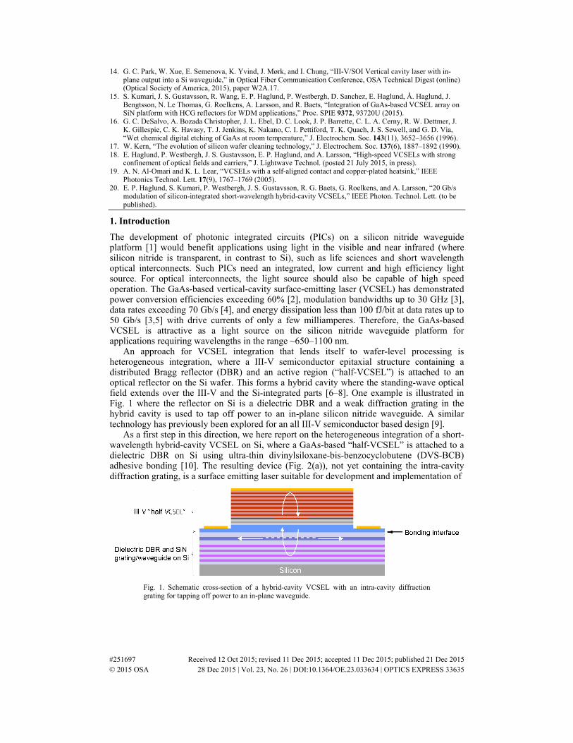
As a first step in this direction, we here report on the heterogeneous integration of a short- wavelength hybrid-cavity VCSEL on Si, where a GaAs-based “half-VCSEL” is attached to a dielectric DBR on Si using ultra-thin divinylsiloxane-bis-benzocyclobutene (DVS-BCB) adhesive bonding [10]. The resulting device (Fig. 2(a)), not yet containing the intra-cavity diffraction grating, is a surface emitting laser suitable for development and implementation of
Fig. 1. Schematic cross-section of a hybrid-cavity VCSEL with an intra-cavity diffraction grating for tapping off power to an in-plane waveguide.
#251697 Received 12 Oct 2015; revised 11 Dec 2015; accepted 11 Dec 2015; published 21 Dec 2015 © 2015 OSA 28 Dec 2015 | Vol. 23, No. 26 | DOI:10.1364/OE.23.033634 | OPTICS EXPRESS 33635
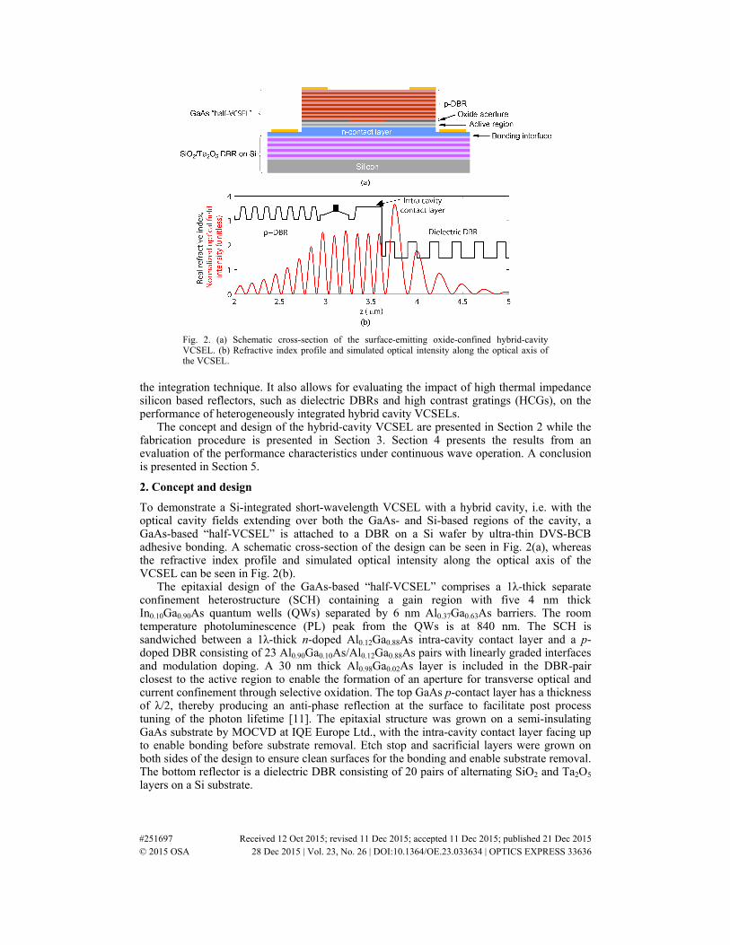
Fig. 2. (a) Schematic cross-section of the surface-emitting oxide-confined hybrid-cavity VCSEL. (b) Refractive index profile and simulated optical intensity along the optical axis of the VCSEL.
the integration technique. It also allows for evaluating the impact of high thermal impedance silicon based reflectors, such as dielectric DBRs and high contrast gratings (HCGs), on the performance of heterogeneously integrated hybrid cavity VCSELs.
The concept and design of the hybrid-cavity VCSEL are presented in Section 2 while the fabrication procedure is presented in Section 3. Section 4 presents the results from an evaluation of the performance characteristics under continuous wave operation. A conclusion is presented in Section 5.
2. Concept and design
To demonstrate a Si-integrated short-wavelength VCSEL with a hybrid cavity, i.e. with the optical cavity fields extending over both the GaAs- and Si-based regions of the cavity, a GaAs-based “half-VCSEL” is attached to a DBR on a Si wafer by ultra-thin DVS-BCB adhesive bonding. A schematic cross-section of the design can be seen in Fig. 2(a), whereas the refractive index profile and simulated optical intensity along the optical axis of the VCSEL can be seen in Fig. 2(b).
The epitaxial design of the GaAs-based “half-VCSEL” comprises a 1λ-thick separate confinement heterostructure (SCH) containing a gain region with five 4 nm thick In0.10Ga0.90As quantum wells (QWs) separated by 6 nm Al0.37Ga0.63As barriers. The room temperature photoluminescence (PL) peak from the QWs is at 840 nm. The SCH is sandwiched between a 1λ-thick n-doped Al0.12Ga0.88As intra-cavity contact layer and a p-doped DBR consisting of 23 Al0.90Ga0.10As/Al0.12Ga0.88As pairs with linearly graded interfaces and modulation doping. A 30 nm thick Al0.98Ga0.02As layer is included in the DBR-pair closest to the active region to enable the formation of an aperture for transverse optical and current confinement through selective oxidation. The top GaAs p-contact layer has a thickness of λ/2, thereby producing an anti-phase reflection at the surface to facilitate post process tuning of the photon lifetime [11]. The epitaxial structure was grown on a semi-insulating GaAs substrate by MOCVD at IQE Europe Ltd., with the intra-cavity contact layer facing up to enable bonding before substrate removal. Etch stop and sacrificial layers were grown on both sides of the design to ensure clean surfaces for the bonding and enable substrate removal. The bottom reflector is a dielectric DBR consisting of 20 pairs of alternating SiO2 and Ta2O5 layers on a Si substrate.
#251697 Received 12 Oct 2015; revised 11 Dec 2015; accepted 11 Dec 2015; published 21 Dec 2015 © 2015 OSA 28 Dec 2015 | Vol. 23, No. 26 | DOI:10.1364/OE.23.033634 | OPTICS EXPRESS 33636
Fig. 3. Fabrication process flow for the silicon-integrated hybrid-cavity VCSEL: the GaAs-based “half-VCSEL” epitaxial structure (a) is attached to the dielectric DBR on silicon, spin-coated with DVS-BCB (b–c). The GaAs substrate is removed, followed by p-contact deposition (d). After the mesa etching and SixNy deposition/opening (e), an oxide aperture is formed (f), the SixNy is removed, and the n-contact is deposited (g). Finally, the structure is planarized with BCB (h) to allow deposition of bondpads (i).
For wavelength division multiplexed (WDM) optical interconnects, the dielectric DBR on Si can be replaced by a silicon nitride HCG on Si since this allows for setting the wavelengths of individual VCSELs in an array by the grating parameters [12]. In addition, a silicon nitride waveguide can be connected to the HCG for in-plane emission, which has been demonstrated for long-wavelength VCSELs [7,13,14]. Together with an integrated wavelength multiplexer, this would enable the fabrication of fully integrated high speed and high efficiency short-wavelength transmitters for WDM optical interconnects [15].
3. Fabrication
The “half-VCSEL” epitaxial structure was attached to the dielectric DBR using ultra-thin DVS-BCB adhesive bonding. The fabrication process flow is shown in Fig. 3. Before bonding, the sacrificial layers (GaAs/AlAs) on top of the intra-cavity contact layer were selectively removed, simultaneously also removing any particles and contaminants. The GaAs layer was selectively removed using citric acid and H2O2, whereas the AlAs layer was removed using diluted HCl. Beneath the AlAs layer there is a very thin layer of GaAs (4 nm) to protect the device layers. To avoid optical band-to-band absorption in the final devices, this
#251697 Received 12 Oct 2015; revised 11 Dec 2015; accepted 11 Dec 2015; published 21 Dec 2015 © 2015 OSA 28 Dec 2015 | Vol. 23, No. 26 | DOI:10.1364/OE.23.033634 | OPTICS EXPRESS 33637
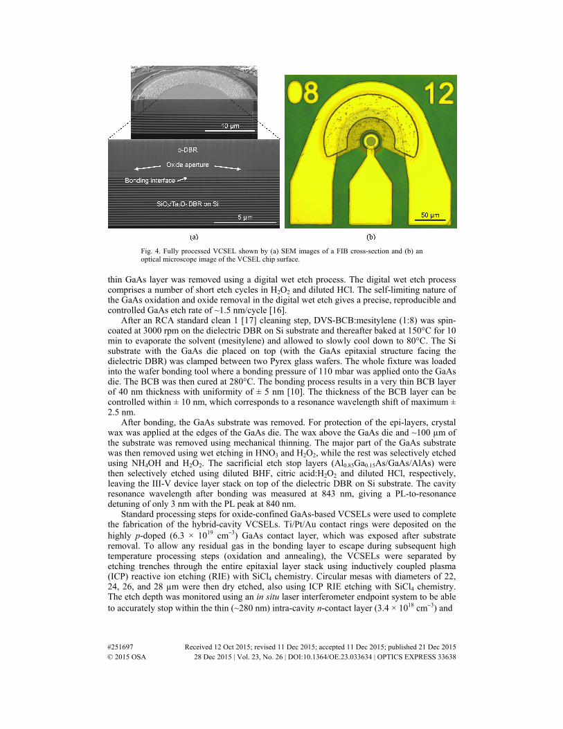
Fig. 4. Fully processed VCSEL shown by (a) SEM images of a FIB cross-section and (b) an optical microscope image of the VCSEL chip surface.
thin GaAs layer was removed using a digital wet etch process. The digital wet etch process comprises a number of short etch cycles in H2O2 and diluted HCl. The self-limiting nature of the GaAs oxidation and oxide removal in the digital wet etch gives a precise, reproducible and controlled GaAs etch rate of ~1.5 nm/cycle [16].
After an RCA standard clean 1 [17] cleaning step, DVS-BCB:mesitylene (1:8) was spin-coated at 3000 rpm on the dielectric DBR on Si substrate and thereafter baked at 150°C for 10 min to evaporate the solvent (mesitylene) and allowed to slowly cool down to 80°C. The Si substrate with the GaAs die placed on top (with the GaAs epitaxial structure facing the dielectric DBR) was clamped between two Pyrex glass wafers. The whole fixture was loaded into the wafer bonding tool where a bonding pressure of 110 mbar was applied onto the GaAs die. The BCB was then cured at 280°C. The bonding process results in a very thin BCB layer of 40 nm thickness with uniformity of ± 5 nm [10]. The thickness of the BCB layer can be controlled within ± 10 nm, which corresponds to a resonance wavelength shift of maximum ± 2.5 nm.
After bonding, the GaAs substrate was removed. For protection of the epi-layers, crystal wax was applied at the edges of the GaAs die. The wax above the GaAs die and ~100 µm of the substrate was removed using mechanical thinning. The major part of the GaAs substrate was then removed using wet etching in HNO3 and H2O2, while the rest was selectively etched using NH4OH and H2O2. The sacrificial etch stop layers (Al0.85Ga0.15As/GaAs/AlAs) were then selectively etched using diluted BHF, citric acid:H2O2 and diluted HCl, respectively, leaving the III-V device layer stack on top of the dielectric DBR on Si substrate. The cavity resonance wavelength after bonding was measured at 843 nm, giving a PL-to-resonance detuning of only 3 nm with the PL peak at 840 nm.
Standard processing steps for oxide-confined GaAs-based VCSELs were used to complete the fabrication of the hybrid-cavity VCSELs. Ti/Pt/Au contact rings were deposited on the highly p-doped (6.3 × 1019 cm−3) GaAs contact layer, which was exposed after substrate removal. To allow any residual gas in the bonding layer to escape during subsequent high temperature processing steps (oxidation and annealing), the VCSELs were separated by etching trenches through the entire epitaxial layer stack using inductively coupled plasma (ICP) reactive ion etching (RIE) with SiCl4 chemistry. Circular mesas with diameters of 22, 24, 26, and 28 µm were then dry etched, also using ICP RIE etching with SiCl4 chemistry. The etch depth was monitored using an in situ laser interferometer endpoint system to be able to accurately stop within the thin (~280 nm) intra-cavity n-contact layer (3.4 × 1018 cm−3) and
#251697 Received 12 Oct 2015; revised 11 Dec 2015; accepted 11 Dec 2015; published 21 Dec 2015 © 2015 OSA 28 Dec 2015 | Vol. 23, No. 26 | DOI:10.1364/OE.23.033634 | OPTICS EXPRESS 33638
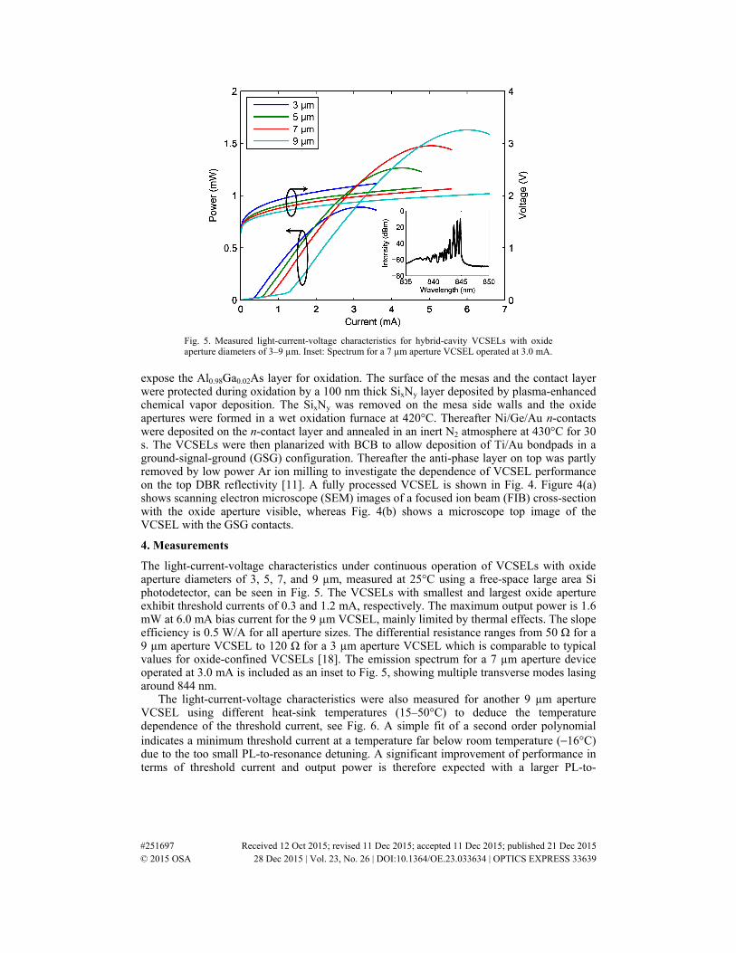
Fig. 5. Measured light-current-voltage characteristics for hybrid-cavity VCSELs with oxide aperture diameters of 3–9 µm. Inset: Spectrum for a 7 µm aperture VCSEL operated at 3.0 mA.
expose the Al0.98Ga0.02As layer for oxidation. The surface of the mesas and the contact layer were protected during oxidation by a 100 nm thick SixNy layer deposited by plasma-enhanced chemical vapor deposition. The SixNy was removed on the mesa side walls and the oxide apertures were formed in a wet oxidation furnace at 420°C. Thereafter Ni/Ge/Au n-contacts were deposited on the n-contact layer and annealed in an inert N2 atmosphere at 430°C for 30 s. The VCSELs were then planarized with BCB to allow deposition of Ti/Au bondpads in a ground-signal-ground (GSG) configuration. Thereafter the anti-phase layer on top was partly removed by low power Ar ion milling to investigate the dependence of VCSEL performance on the top DBR reflectivity [11]. A fully processed VCSEL is shown in Fig. 4. Figure 4(a) shows scanning electron microscope (SEM) images of a focused ion beam (FIB) cross-section with the oxide aperture visible, whereas Fig. 4(b) shows a microscope top image of the VCSEL with the GSG contacts.
4. Measurements
The light-current-voltage characteristics under continuous operation of VCSELs with oxide aperture diameters of 3, 5, 7, and 9 µm, measured at 25°C using a free-space large area Si photodetector, can be seen in Fig. 5. The VCSELs with smallest and largest oxide aperture exhibit threshold currents of 0.3 and 1.2 mA, respectively. The maximum output power is 1.6 mW at 6.0 mA bias current for the 9 µm VCSEL, mainly limited by thermal effects. The slope efficiency is 0.5 W/A for all aperture sizes. The differential resistance ranges from 50 Ω for a 9 µm aperture VCSEL to 120 Ω for a 3 µm aperture VCSEL which is comparable to typical values for oxide-confined VCSELs [18]. The emission spectrum for a 7 µm aperture device operated at 3.0 mA is included as an inset to Fig. 5, showing multiple transverse modes lasing around 844 nm.
The light-current-voltage characteristics were also measured for another 9 µm aperture VCSEL using different heat-sink temperatures (15–50°C) to deduce the temperature dependence of the threshold current, see Fig. 6. A simple fit of a second order polynomial indicates a minimum threshold current at a temperature far below room temperature (−16°C) due to the too small PL-to-resonance detuning. A significant improvement of performance in terms of threshold current and output power is therefore expected with a larger PL-to-
#251697 Received 12 Oct 2015; revised 11 Dec 2015; accepted 11 Dec 2015; published 21 Dec 2015 © 2015 OSA 28 Dec 2015 | Vol. 23, No. 26 | DOI:10.1364/OE.23.033634 | OPTICS EXPRESS 33639
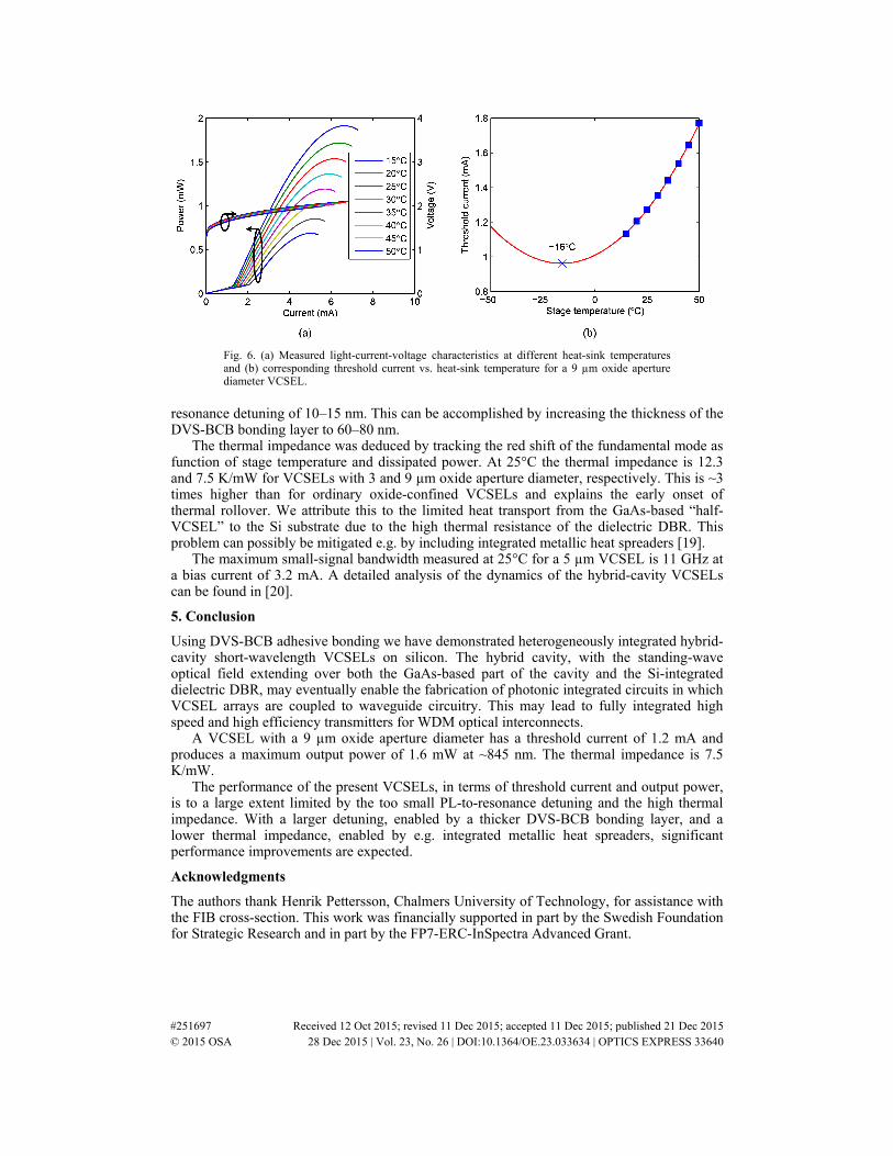
Fig. 6. (a) Measured light-current-voltage characteristics at different heat-sink temperatures and (b) corresponding threshold current vs. heat-sink temperature for a 9 µm oxide aperture diameter VCSEL.
resonance detuning of 10–15 nm. This can be accomplished by increasing the thickness of the DVS-BCB bonding layer to 60–80 nm.
The thermal impedance was deduced by tracking the red shift of the fundamental mode as function of stage temperature and dissipated power. At 25°C the thermal impedance is 12.3 and 7.5 K/mW for VCSELs with 3 and 9 µm oxide aperture diameter, respectively. This is ~3 times higher than for ordinary oxide-confined VCSELs and explains the early onset of thermal rollover. We attribute this to the limited heat transport from the GaAs-based “half-VCSEL” to the Si substrate due to the high thermal resistance of the dielectric DBR. This problem can possibly be mitigated e.g. by including integrated metallic heat spreaders [19].
The maximum small-signal bandwidth measured at 25°C for a 5 µm VCSEL is 11 GHz at a bias current of 3.2 mA. A detailed analysis of the dynamics of the hybrid-cavity VCSELs can be found in [20].
5. Conclusion
Using DVS-BCB adhesive bonding we have demonstrated heterogeneously integrated hybrid-cavity short-wavelength VCSELs on silicon. The hybrid cavity, with the standing-wave optical field extending over both the GaAs-based part of the cavity and the Si-integrated dielectric DBR, may eventually enable the fabrication of photonic integrated circuits in which VCSEL arrays are coupled to waveguide circuitry. This may lead to fully integrated high speed and high efficiency transmitters for WDM optical interconnects.
A VCSEL with a 9 µm oxide aperture diameter has a threshold current of 1.2 mA and produces a maximum output power of 1.6 mW at ~845 nm. The thermal impedance is 7.5 K/mW.
The performance of the present VCSELs, in terms of threshold current and output power, is to a large extent limited by the too small PL-to-resonance detuning and the high thermal impedance. With a larger detuning, enabled by a thicker DVS-BCB bonding layer, and a lower thermal impedance, enabled by e.g. integrated metallic heat spreaders, significant performance improvements are expected.
Acknowledgments
The authors thank Henrik Pettersson, Chalmers University of Technology, for assistance with the FIB cross-section. This work was financially supported in part by the Swedish Foundation for Strategic Research and in part by the FP7-ERC-InSpectra Advanced Grant.
#251697 Received 12 Oct 2015; revised 11 Dec 2015; accepted 11 Dec 2015; published 21 Dec 2015 © 2015 OSA 28 Dec 2015 | Vol. 23, No. 26 | DOI:10.1364/OE.23.033634 | OPTICS EXPRESS 33640