toshiba cdmos integrated circuit silicon monolithic
TRANSCRIPT

TC78H653FTG
2018-11-13 1
Toshiba CDMOS Integrated Circuit Silicon Monolithic
TC78H653FTG 1.8-V Dual H-bridge driver IC The TC78H653FTG is a dual H-bridge driver IC for one or two DC brushed motors or one Stepping motor which incorporates DMOS with low ON resistance in output transistors. The TC78H653FTG has selectable forward, reverse, stop or brake mode. Over current detection, thermal shutdown, and under voltage lockout functions are implemented. The device is housed in a compact QFN-16 3.0 mm×3.0 mm package.
Features • Power supply maximum voltage: 8.0 V • Power supply operating voltage: 1.8 V to 7.5 V • Brushed motor output current ratings (DC)
4.0A (max) in Large mode 2.0A (max) in Small mode
• Brushed motor output current ratings (Peak) 5.0A (max) at 10 ms or less in Large mode 2.5A (max) at 10 ms or less in Small mode
• Stepping motor output current ratings (DC) 2.0A (DC) 2.5A (peak)
• Output ON resistance 0.11Ω (typ.) (Ta = 25 °C, Sum of upper and lower side, VM = 5.0 V, Large mode) 0.22 Ω (typ.) (Ta = 25 °C, Sum of upper and lower side, VM = 5.0 V, Small mode)
• Built-in standby function: Consumption current 0 μA (typ.) • Built-in cross conduction protection circuit • Built-in over current detection (ISD), thermal shutdown (TSD), and under voltage lockout
(UVLO) • Selectable Forward / Reverse / Stop / Brake modes • Package: P-VQFN16-0303-0.50-001(3.0 mm×3.0 mm)
P-VQFN16-0303-0.50-001 Weight: 0.02 g (typ.)
© 2018 Toshiba Electronic Devices & Storage Corporation

TC78H653FTG
2018-11-13 2
Pin Assignment (Top View) Note: In DC Brushed motor Large mode (LARGE pin is set to High), pins OUT1 and OUT2 are connected as OUT+
pin and pins OUT3 and OUT4 pin are connected as OUT- pin. Then Large mode is controlled with IN1/ENB_A pin and IN2/PHA_A pins.
IN4/PHA_B
NC
IN2/PHA_A
IN3/ENB_B
IN1/ENB_A
STBY
MODE LARGE VM
OUT2
GND NC
1
2
3
4
5 6 7 8
9
10
11
12
13 14 15 16
OUT1
OUT3
OUT4
GND

TC78H653FTG
2018-11-13 3
Block Diagram
Note: The block diagram, functional blocks or constants may be omitted or simplified for explanatory purposes.
Pin Functions
Pin name Pin number Functional description Remarks
IN4/PHA_B 1 Control input Refer to the section of “Input/Output Functions”. IN3/ENB_B 2 Control input Refer to the section of “Input/Output Functions”.
NC 3 No connection Please use this terminal open. IN1/ENB_A 4 Control input Refer to the section of “Input/Output Functions”. IN2/PHA_A 5 Control input Refer to the section of “Input/Output Functions”.
STBY 6 Control input Refer to the section of “Input/Output Functions”. NC 7 No connection Please use this terminal open.
GND 8 GND pin — OUT2 9 Output Motor coil connection pin OUT1 10 Output Motor coil connection pin OUT3 11 Output Motor coil connection pin OUT4 12 Output Motor coil connection pin GND 13 GND pin — VM 14 Power supply pin Operating range is from 1.8 V to 7.5 V.
LARGE 15 Control input Refer to the section of “Input/Output Functions”. MODE 16 Control input Refer to the section of “Input/Output Functions”.
OUT1 OUT2
OUT3 OUT4
GND
VM Regulator
UVLO
IN1/ENB_A 150 kΩ
37 kΩ
TSD
ISD
150 kΩ 37 kΩ
150 kΩ 37 kΩ
150 kΩ 37 kΩ
IN2/PHA_A
IN3/ENB_B
IN4/PHA_B
150 kΩ 37 kΩ STBY
150 kΩ 37 kΩ LARGE
150 kΩ 37 kΩ
Control Circuit
MODE

TC78H653FTG
2018-11-13 4
Input / Output Functions IN Input mode (MODE=L), in Small mode (LARGE=L)
MODE LARGE STBY IN1/ ENB_A
IN2/ PHA_A
IN3/ ENB_B
IN4/ PHA_B OUT1 OUT2 OUT3 OUT4 Mode
L L
H H L X X H L X X Forward H L H X X L H X X Reverse H X X H L X X H L Forward H X X L H X X L H Reverse H H H H H L L L L Short brake
H L L L L OFF OFF OFF OFF Stop L X X X X OFF OFF OFF OFF Standby
Note: 2 H-Bridge can be programmed and operate simultaneously. Note: X are Don’t Care. IN Input mode (MODE=L), in Large mode (LARGE=H)
MODE LARGE STBY IN1/ ENB_A
IN2/ PHA_A
IN3/ ENB_B
IN4/ PHA_B OUT1 OUT2 OUT3 OUT4 Mode
L H
H H L X X H H L L Forward H L H X X L L H H Reverse H H H X X L L L L Short brake H L L X X OFF OFF OFF OFF Stop L X X X X OFF OFF OFF OFF Standby
Note: X are Don’t Care. PHASE input mode (MODE=H) in Small mode (LARGE=L)
MODE LARGE STBY IN1/ ENB_A
IN2/ PHA_A
IN3/ ENB_B
IN4/ PHA_B OUT1 OUT2 OUT3 OUT4 Mode
H L
H H H X X H L X X Forward H H L X X L H X X Reverse
H X X H H X X H L Forward H X X H L X X L H Reverse H L X L X OFF OFF OFF OFF Stop L X X X X OFF OFF OFF OFF Standby
Note: 2 H-Bridge can be programmed and operate simultaneously. Note: X are Don’t Care. PHASE input mode (MODE=H), Large mode (LARGE=H)
MODE LARGE STBY IN1/ ENB_A
IN2/ PHA_A
IN3/ ENB_B
IN4/ PHA_B OUT1 OUT2 OUT3 OUT4 Mode
H H
H H H X X H H L L Forward H H L X X L L H H Reverse H L X L X OFF OFF OFF OFF Stop
L X X X X OFF OFF OFF OFF Standby Note: X are Don’t Care.
TC78H653FTG
2018-11-13 5
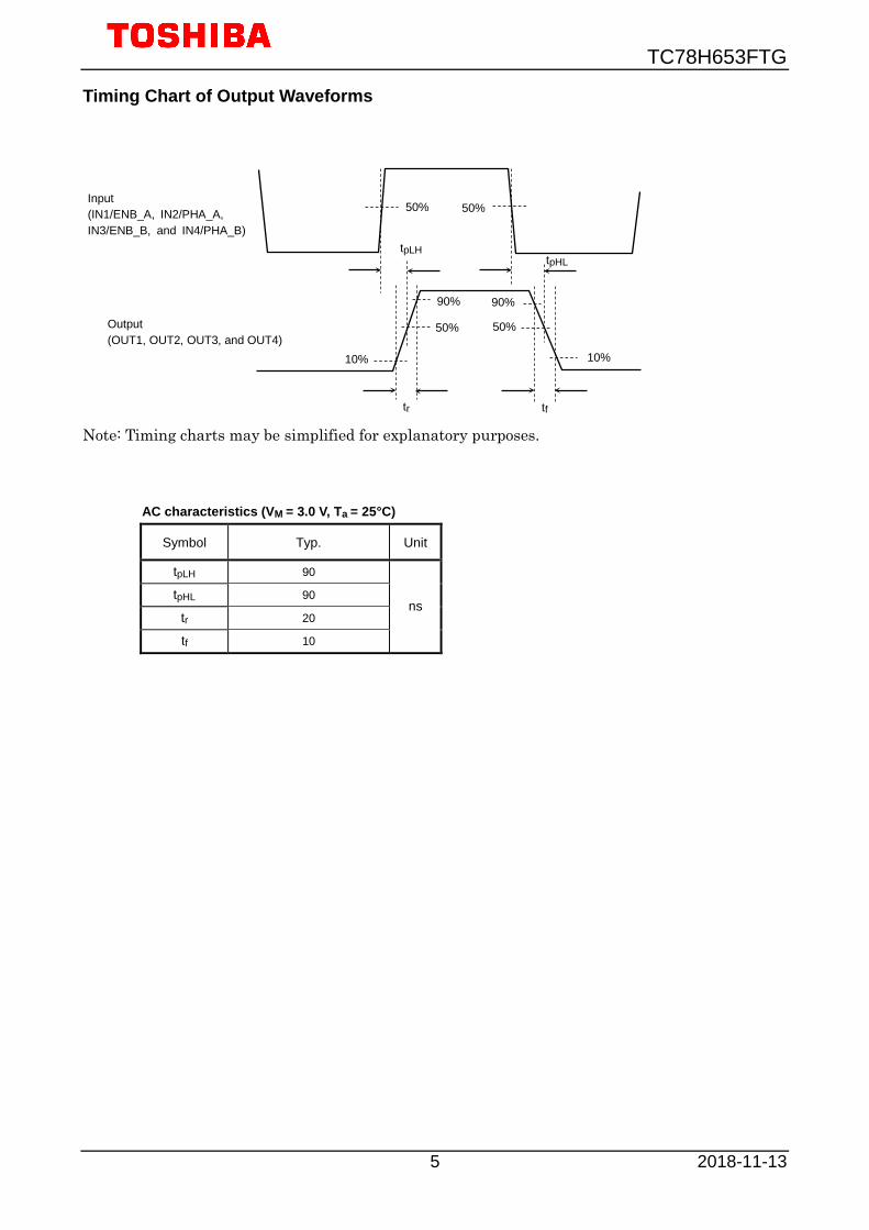
Timing Chart of Output Waveforms
Note: Timing charts may be simplified for explanatory purposes.
AC characteristics (VM = 3.0 V, Ta = 25°C)
Symbol Typ. Unit
tpLH 90
ns tpHL 90
tr 20
tf 10
Output (OUT1, OUT2, OUT3, and OUT4)
90%
10%
50%
tpLH
tr
50%
tpHL
90%
10%
tf
Input (IN1/ENB_A, IN2/PHA_A, IN3/ENB_B, and IN4/PHA_B)
50% 50%

TC78H653FTG
2018-11-13 6
Absolute Maximum Ratings (Ta = 25°C)
Characteristics Symbol Rating Unit Remarks
Power supply voltage VM 8.0 V ―
Input voltage VIN −0.3 to 6 V ―
Output current IOUT
4.0 A In Large mode
2.0 A In Small mode
5.0 A In Large mode, Peak at 10 ms
2.5 A In Small mode, Peak at 10 ms
Output DMOS body diode forward current If
2.0 A In Small mode
4.0 A In Large mode
Power dissipation PD 1.79 W ―
Operating range Topr −40 to 105 °C ―
Storage temperature Tstg −55 to 150 °C ―
Note: When mounted on the board (JEDEC 4 layers), if Ta exceeds 25°C, it is necessary to do the derating with 14.3mW/°C.
Back-EMF While a motor is rotating, there is a timing at which power is fed back to the power supply. At that timing, the motor current recirculates back to the power supply due to the effect of the motor back-EMF. If the power supply does not have enough current sinking capability, the power supply and output pins of the device may rise above the rated voltage of 8.0 V. The magnitude of the motor back-EMF varies with usage conditions and motor characteristics. It must be fully verified that there is no risk that the device or other components will not be damaged or failed due to the motor back-EMF. When the power is fed back to the power supply, the body diode of the output DMOS may turn on and a regenerative current may flow. At this time, the voltage applied to one of the output pins may become a negative value by the voltage of the body diode (Vf). It is not a concern if the current of the body diode (If) is within the rated value (shown in above table) or less, it is no problem. Over Current Detection (ISD) and Thermal Shutdown (TSD) The ISD and TSD circuits are only intended to provide temporary protection against irregular conditions such as an output short-circuits; they do not necessarily guarantee the complete IC safety. If the device is used beyond the specified operating ranges, these circuits may not operate properly: then the device may be damaged due to an output short-circuit. The ISD circuit is only intended to provide a temporary protection against an output short-circuit. If such condition persists for a long time, the device may be damaged due to overstress. Overcurrent conditions must be removed immediately by external hardware. IC Mounting Do not insert devices incorrectly or in the wrong orientation. Otherwise, it may cause breakdown, damage and/or deterioration of the device.
Operating Conditions (Ta = −40 to 105°C)
Characteristics Symbol Min Typ. Max Unit Remarks
Power supply voltage VM 1.8 3.0 7.5 V ―
Output current IOUT ― ― 4.0 A In Large mode, VM =5.0V
― ― 2.0 A In Small mode, VM =5.0V
PWM frequency fPWM ― ― 500 kHz Duty=50%

TC78H653FTG
2018-11-13 7
Electrical Characteristics (Unless otherwise specified, VM = 1.8 to 7.0 V, Ta = 25°C)
Characteristics Symbol Test condition Min Typ. Max Unit
Consumption current ICC (W)
Forward / Reverse mode, VM = 3.0 V, Output open ― 0.6 1.0 mA
ICC (STB) Standby mode, VM = 3.0 V ― 0 0.22 μA
Control circuit
Input voltage
VIH1 VM = 1.8 V 1.5 ― 5.5
V
VIH2 VM = 3.0 V 1.7 ― 5.5
VIH3 VM = 5.0 V 2.0 ― 5.5
VIH4 VM = 7.0 V 2.0 ― 5.5
VIL ― - 0.3 ― 0.5
Input current IIH VIN=3.0 V 10 16 22
μA IIL ― ― ― 1.0
ON-resistance between drain and source of output transistor
(Sum of upper and lower side)
RON(D-S) IOUT = 1.0 A , VM =5.0 V
In Small mode ― 0.22 0.35 Ω
RON(D-S) IOUT = 1.0 A , VM =5.0 V
In Large mode ― 0.11 0.175 Ω
Output leakage current IOH
VM = 3.0 V ― ― 0.5
μA IOL ― ― 0.5
Output DMOS body diode forward voltage Vf If = 0.4 A, VM = 5.0 V ― 0.7 1.0 V

TC78H653FTG
2018-11-13 8
(Reference data) PD - Ta Characteristics
0.0
0.2
0.4
0.6
0.8
1.0
1.2
1.4
1.6
1.8
2.0
0 25 50 75 100 125 150
P D(W
)
Ta (°C)
PD-Ta
When mounted on the board (JEDEC 4 layers) Note: Characteristics shown above are reference values and not guaranteed.

TC78H653FTG
2018-11-13 9
Fault Detections
Thermal Shut Down (TSD) When the junction temperature (Tj) of the IC exceeds 170°C (typ.), all outputs are turned off. When the junction temperature (Tj) falls by 40°C (typ.) or more, it returns to the normal mode. Note: Above TSD operation and release thresholds are reference values, and are not guaranteed. Over Current Detection (ISD) When the IC detects an over current in the output transistors (exceeding ISD operation threshold value), all outputs are turned off. It has a dead band time of 1.5 μs (typ.) to avoid ISD false triggering by switching noise. ISD releases when one of the followings occur: 1. Operation mode is re-configured after setting to the standby mode, set STBY to L then H. 2. Recycle the power supply.
Characteristics in Small mode Characteristic in Large mode
0.0
1.0
2.0
3.0
4.0
5.0
6.0
7.0
1 2 3 4 5 6 7
ISD
thre
shol
d (A
)
VM (V)
VM-ISD threshold (Reference data)
0.0
1.0
2.0
3.0
4.0
5.0
6.0
7.0
1 2 3 4 5 6 7
ISD
thre
shol
d (A
)
VM (V)
VM-ISD threshold (Reference data)
Note: Above ISD operation threshold value and dead band time are reference values, and are not
guaranteed. Under Voltage Lockout (UVLO) When VM pin voltage falls to less than 1.7 V (typ.), all outputs are turned off. UVLO is released when VM pin voltage rises at or above 1.7 V (typ.). Note: Above UVLO operation and release thresholds are reference values, and are not guaranteed.
Dead band time: 1.5 μs (typ.) Output OFF
Motor output current
ISD threshold
H bridge high side
Pch DMOS
H bridge lower side
Nch DMOS
H bridge lower side
Nch DMOS
H bridge high side
Pch DMOS

TC78H653FTG
2018-11-13 10
Examples of Application Circuit
In Small mode for two Brushed motors (LARGE = L)
In Large mode for one Brushed motor (LARGE = H)
Note1: A power supply ceramics capacitor for noise absorption should be connected as close to the IC as possible.
Note2: Utmost care is necessary in the design of VM and GND line since the IC may be destroyed by short-circuiting between outputs, by short-circuiting to the power supply or ground, or by short-circuiting between contiguous pins.
M
IN2/PHA_A
IN1/ENB_A
GND
OUT1
OUT2
TC78H653FTG
VM
VM
OUT3
OUT4
IN4/PHA_B
IN3/ENB_B
Note 1
M
LARGE
MODE
OUT1
OUT2
TC78H653FTG
VM
VM
OUT3
OUT4
Note 1
M
STBY
IN2/PHA_A
IN1/ENB_A
LARGE
MODE
STBY
GND

TC78H653FTG
2018-11-13 11
Package Dimensions
P-VQFN16-0303-0.50-001 Unit: mm
Weight: 0.02 g (Typ.)

TC78H653FTG
2018-11-13 12
Notes on Contents 1. Block Diagrams
Some of the functional blocks, circuits, or constants in the block diagram may be omitted or simplified for explanatory purposes.
2. Equivalent Circuits
The equivalent circuit diagrams may be simplified or some parts of them may be omitted for explanatory purposes.
3. Timing Charts
Timing charts may be simplified for explanatory purposes. 4. Application Circuits
The application circuits shown in this document are provided for reference purposes only. Thorough evaluation is required, especially at the mass production design stage. Providing these application circuit examples does not grant a license for industrial property rights.
5. Test Circuits
Components in the test circuits are used only to obtain and confirm the device characteristics. These components and circuits are not guaranteed to prevent malfunction or failure from occurring in the application equipment.
IC Usage Considerations
Notes on handling of ICs [1] The absolute maximum ratings of a semiconductor device are a set of ratings that must not be
exceeded, even for a moment. Do not exceed any of these ratings. Exceeding the rating(s) may cause the device breakdown, damage or deterioration, and may result injury by explosion or combustion.
[2] Use an appropriate power supply fuse to ensure that a large current does not continuously flow in
case of over current and/or IC failure. The IC will fully break down when used under conditions that exceed its absolute maximum ratings, when the wiring is routed improperly or when an abnormal pulse noise occurs from the wiring or load, causing a large current to continuously flow and the breakdown can lead smoke or ignition. To minimize the effects of the flow of a large current in case of breakdown, appropriate settings, such as fuse capacity, fusing time and insertion circuit location, are required.
[3] If your design includes an inductive load such as a motor coil, incorporate a protection circuit into
the design to prevent device malfunction or breakdown caused by the current resulting from the inrush current at power ON or the negative current resulting from the back electromotive force at power OFF. IC breakdown may cause injury, smoke or ignition. Use a stable power supply with ICs with built-in protection functions. If the power supply is unstable, the protection function may not operate, causing IC breakdown. IC breakdown may cause injury, smoke or ignition.
[4] Do not insert devices in the wrong orientation or incorrectly. Make sure that the positive and negative terminals of power supplies are connected properly. Otherwise, the current or power consumption may exceed the absolute maximum rating, and exceeding the rating(s) may cause the device breakdown, damage or deterioration, and may result injury by explosion or combustion. In addition, do not use any device that is applied the current with inserting in the wrong orientation or incorrectly even just one time.

TC78H653FTG
2018-11-13 13
Points to remember on handling of ICs (1) Thermal Shutdown Circuit
Thermal shutdown circuits do not necessarily protect ICs under all circumstances. If the thermal shutdown circuits operate against the over temperature, clear the heat generation status immediately. Depending on the method of use and usage conditions, such as exceeding absolute maximum ratings can cause the thermal shutdown circuit to not operate properly or IC breakdown before operation.
(2) Heat Radiation Design
In using an IC with large current flow such as power amp, regulator or driver, please design the device so that heat is appropriately radiated, not to exceed the specified junction temperature (TJ) at any time and condition. These ICs generate heat even during normal use. An inadequate IC heat radiation design can lead to decrease in IC life, deterioration of IC characteristics or IC breakdown. In addition, please design the device taking into considerate the effect of IC heat radiation with peripheral components.
(3) Back-EMF
When a motor rotates in the reverse direction, stops or slows down abruptly, a current flow back to the motor’s power supply due to the effect of back-EMF. If the current sink capability of the power supply is small, the device’s motor power supply and output pins might be exposed to conditions beyond absolute maximum ratings. To avoid this problem, take the effect of back-EMF into consideration in system design.
TC78H653FTG
2018-11-13 14
RESTRICTIONS ON PRODUCT USE Toshiba Corporation and its subsidiaries and affiliates are collectively referred to as “TOSHIBA”. Hardware, software and systems described in this document are collectively referred to as “Product”.
• TOSHIBA reserves the right to make changes to the information in this document and related Product without notice.
• This document and any information herein may not be reproduced without prior written permission from TOSHIBA. Even with TOSHIBA's written permission, reproduction is permissible only if reproduction is without alteration/omission.
• Though TOSHIBA works continually to improve Product's quality and reliability, Product can malfunction or fail. Customers are responsible for complying with safety standards and for providing adequate designs and safeguards for their hardware, software and systems which minimize risk and avoid situations in which a malfunction or failure of Product could cause loss of human life, bodily injury or damage to property, including data loss or corruption. Before customers use the Product, create designs including the Product, or incorporate the Product into their own applications, customers must also refer to and comply with (a) the latest versions of all relevant TOSHIBA information, including without limitation, this document, the specifications, the data sheets and application notes for Product and the precautions and conditions set forth in the "TOSHIBA Semiconductor Reliability Handbook" and (b) the instructions for the application with which the Product will be used with or for. Customers are solely responsible for all aspects of their own product design or applications, including but not limited to (a) determining the appropriateness of the use of this Product in such design or applications; (b) evaluating and determining the applicability of any information contained in this document, or in charts, diagrams, programs, algorithms, sample application circuits, or any other referenced documents; and (c) validating all operating parameters for such designs and applications. TOSHIBA ASSUMES NO LIABILITY FOR CUSTOMERS' PRODUCT DESIGN OR APPLICATIONS.
• PRODUCT IS NEITHER INTENDED NOR WARRANTED FOR USE IN EQUIPMENTS OR SYSTEMS THAT REQUIRE EXTRAORDINARILY HIGH LEVELS OF QUALITY AND/OR RELIABILITY, AND/OR A MALFUNCTION OR FAILURE OF WHICH MAY CAUSE LOSS OF HUMAN LIFE, BODILY INJURY, SERIOUS PROPERTY DAMAGE AND/OR SERIOUS PUBLIC IMPACT ("UNINTENDED USE"). Except for specific applications as expressly stated in this document, Unintended Use includes, without limitation, equipment used in nuclear facilities, equipment used in the aerospace industry, lifesaving and/or life supporting medical equipment, equipment used for automobiles, trains, ships and other transportation, traffic signaling equipment, equipment used to control combustions or explosions, safety devices, elevators and escalators, and devices related to power plant. IF YOU USE PRODUCT FOR UNINTENDED USE, TOSHIBA ASSUMES NO LIABILITY FOR PRODUCT. For details, please contact your TOSHIBA sales representative or contact us via our website.
• Do not disassemble, analyze, reverse-engineer, alter, modify, translate or copy Product, whether in whole or in part.
• Product shall not be used for or incorporated into any products or systems whose manufacture, use, or sale is prohibited under any applicable laws or regulations.
• The information contained herein is presented only as guidance for Product use. No responsibility is assumed by TOSHIBA for any infringement of patents or any other intellectual property rights of third parties that may result from the use of Product. No license to any intellectual property right is granted by this document, whether express or implied, by estoppel or otherwise.
• ABSENT A WRITTEN SIGNED AGREEMENT, EXCEPT AS PROVIDED IN THE RELEVANT TERMS AND CONDITIONS OF SALE FOR PRODUCT, AND TO THE MAXIMUM EXTENT ALLOWABLE BY LAW, TOSHIBA (1) ASSUMES NO LIABILITY WHATSOEVER, INCLUDING WITHOUT LIMITATION, INDIRECT, CONSEQUENTIAL, SPECIAL, OR INCIDENTAL DAMAGES OR LOSS, INCLUDING WITHOUT LIMITATION, LOSS OF PROFITS, LOSS OF OPPORTUNITIES, BUSINESS INTERRUPTION AND LOSS OF DATA, AND (2) DISCLAIMS ANY AND ALL EXPRESS OR IMPLIED WARRANTIES AND CONDITIONS RELATED TO SALE, USE OF PRODUCT, OR INFORMATION, INCLUDING WARRANTIES OR CONDITIONS OF MERCHANTABILITY, FITNESS FOR A PARTICULAR PURPOSE, ACCURACY OF INFORMATION, OR NONINFRINGEMENT.
• Do not use or otherwise make available Product or related software or technology for any military purposes, including without limitation, for the design, development, use, stockpiling or manufacturing of nuclear, chemical, or biological weapons or missile technology products (mass destruction weapons). Product and related software and technology may be controlled under the applicable export laws and regulations including, without limitation, the Japanese Foreign Exchange and Foreign Trade Law and the U.S. Export Administration Regulations. Export and re-export of Product or related software or technology are strictly prohibited except in compliance with all applicable export laws and regulations.
• Please contact your TOSHIBA sales representative for details as to environmental matters such as the RoHS compatibility of Product. Please use Product in compliance with all applicable laws and regulations that regulate the inclusion or use of controlled substances, including without limitation, the EU RoHS Directive. TOSHIBA ASSUMES NO LIABILITY FOR DAMAGES OR LOSSES OCCURRING AS A RESULT OF NONCOMPLIANCE WITH APPLICABLE LAWS AND REGULATIONS.
https://toshiba.semicon-storage.com/