simulation-iss4
TRANSCRIPT

SYNERGIE CADConfidential
Page 1

SYNERGIE CADConfidential
Page 2
Design EngineeringSimulation Overview - Tool Set
• ANSYS HFSS software is the industry-standard simulation tool for 3-D full-wave electromagnetic field simulation and is essential for the design of high-frequency and high-speed circuit design.
– Provides accuracy for the design of high-speed circuits, test sockets, PCB interconnects, high-frequency components and RF/microwave components.
– Evaluate signal quality, including transmission path losses, reflection losses due to impedance mismatches, parasitic coupling and radiation.
– Visualize 3-D electromagnetic fields.
• ANSYS SIWave to analyse complete designs (includes multiple, arbitrarily shaped power/ground layers, vias, signal traces and circuit elements).
– Perform complete signal-integrity and power-integrity analysis from DC to beyond 10 GHz.
• Extract matrix parameters (S,Y, Z parameters), of signal nets and power distribution networks directly from EDA layout databases*.
• Aids in the identification of signal-integrity and power-integrity problems and is critical to first-pass system success.
* ODB++ is used as a common transfer method. It must be verified if the ODB++ file created by a particular package is compatible.

SYNERGIE CADConfidential
Page 3
SimulationEDA Data Import
• ODB++ data files from the EDA Layout tool are directly imported.– Synergie-Cad can also provide simulation as a separate service.
• Measurement ports are place at the required points on the layout• Extraction of matrix parameters (S,Y, Z parameters) for analysis.• Cut-out sections of the layout to perform detailed 3D full-wave simulation of
High-frequency and RF/microwave areas.
Verigy 93K 9.5”, Vertical Probe Card, 32 Layer

SYNERGIE CADConfidential
Page 4
Simulation - Signal Integrity Matrix Data (S,Y,Z, Parameters) Analysis
Transmission and Return Loss Signal Isolation
RF, Inductance and Capacitance Measurements
RF, Impedance, VSWR, Matching

SYNERGIE CADConfidential
Page 5
Simulation - Signal IntegrityTDR Analysis
Open circuit seen:~7ns / 2 (return time of signal path) = ~3ns
Disturbance from Components
Tester pogo, t = 0ns

SYNERGIE CADConfidential
Page 6
Simulation - Signal IntegrityMatrix Data Exported for use with Circuit
Simulators
• Terminal data exported• Port[1] = N1_1022• Port[2] = P1_1022• Port[3] = N2_1022• Port[4] = N1_1025• Port[5] = N2_1025• Port[6] = N1_1021• Port[7] = N2_1021• Port[8] = N1_1024• Port[9] = N2_1024• Port[10] = P2_1022• Port[11] = P1_1025• Port[12] = P2_1025• Port[13] = P1_1021• Port[14] = P2_1021• Port[15] = P1_1024• Port[16] = P2_1024
S7,6
Net: n1021Net: p1021
S6,6
S13,13
S7,7
S14,14
S14,13
Port[6] = N1_1021 Port[7] = N2_1021
Port[13] = P1_1021 Port[14] = P2_1021
Example, Net 1021
Touchstone S-Parameter data files
SYNERGIE CADConfidential
Page 7
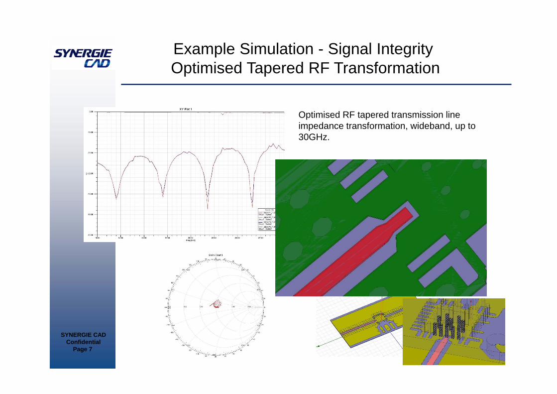
Example Simulation - Signal IntegrityOptimised Tapered RF Transformation
Optimised RF tapered transmission lineimpedance transformation, wideband, up to 30GHz.

SYNERGIE CADConfidential
Page 8
Simulation – Usage Scenario #1
• Simulate the performance of standard cantilever needle at RF frequencies.
• The complete needle assembly, epoxy ring and PCB is included in the model.
Port 1 (S1)Needle Tip
Port 2 (S2)PCB launch track
Simulation results.Freq. sweep: 1GHz to 10Ghz.

SYNERGIE CADConfidential
Page 9
Simulation – Usage Scenario #2
• Model of the needle assembly used to understand the inductance of a cantilever needle at ~920MHz.
• S-Parameters simulated for S11, S22.
SYNERGIE CADConfidential
Page 10
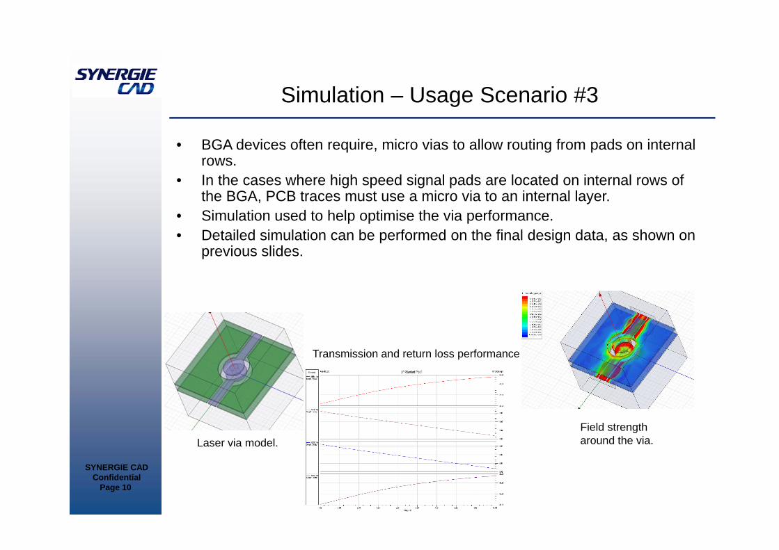
• BGA devices often require, micro vias to allow routing from pads on internal rows.
• In the cases where high speed signal pads are located on internal rows of the BGA, PCB traces must use a micro via to an internal layer.
• Simulation used to help optimise the via performance.• Detailed simulation can be performed on the final design data, as shown on
previous slides.
Field strengtharound the via.
Transmission and return loss performance
Laser via model.
Simulation – Usage Scenario #3

SYNERGIE CADConfidential
Page 11
Example Simulation - Signal IntegrityOptimised 50 ohm Via, Transmission and
Reflection Loss

SYNERGIE CADConfidential
Page 12
Simulation – Usage Scenario #4
• Possible to simulate and include as part of a larger simulation the performance of springs pins from a socket body or vertical probe head.
0
1
2
3
4
5
0 1 2 3 4 5 6 7Frequency (GHz)
Indu
ctan
ce (n
H)
-3
-2
-1
0
0 1 2 3 4 5 6 7Frequency (GHz)
Inse
rtion
Los
s S2
1(dB
)
-60
-50
-40
-30
-20
-10
0
0 1 2 3 4 5 6 7Frequency (GHz)
Ret
urn
Loss
S11
(dB)
Fig.1 Inductance
Fig.2 Insertion Loss Fig.3 Insertion Loss
SYNERGIE CADConfidential
Page 13
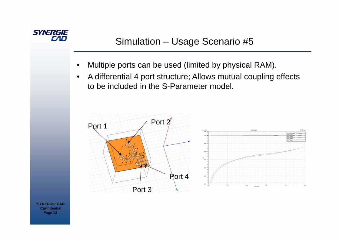
Simulation – Usage Scenario #5
• Multiple ports can be used (limited by physical RAM).• A differential 4 port structure; Allows mutual coupling effects
to be included in the S-Parameter model.
Port 4
Port 2
Port 3
Port 1

SYNERGIE CADConfidential
Page 14
Simulation – Exported Data
• S-Parameter data file can be provided to customers, to allow in circuit simulation of the PCB before it is manufactured.
• Allows for confidence in the PCB layout and design before committing to the manufacture.
• Can save time and cost, if in the unlikely event a problem is found on the PCB after manufacture during functional test.
! Touchstone file from project RF-probe! Exported from HFSS 12.0.0# GHZ S DB R 50.000000! Modal data exported! Port[1] = 1:1! Port[2] = 2:11.000000000000000E+000 -1.591625431137832E+001 6.038651181469610E+001 -1.717771359540705E-001 1.574416881357343E+002 -1.717771359776334E-001 1.574416881357361E+002 -1.591195795430505E+001 7.239763240570214E+001 ! Gamma ! 3.208151732005790E-001 3.325143588579720E+001 5.466199417260070E-001 2.153677718539890E+001 ! Port Impedance 5.000000000000000E+001 0.000000000000000E+000 5.000000000000000E+001 0.000000000000000E+000
1.020000000000000E+000 -1.576155621619889E+001 5.985904360802454E+001 -1.766716037997347E-001 1.570001641968290E+002 -1.766716038225167E-001 1.570001641968333E+002 -1.575655129063723E+001 7.207979692165326E+001 ! Gamma ! 3.255003515711610E-001 3.391460264595060E+001 5.522104634251370E-001 2.196188115903890E+001 ! Port Impedance 5.000000000000000E+001 0.000000000000000E+000 5.000000000000000E+001 0.000000000000000E+000
1.040000000000000E+000 -1.561036871747129E+001 5.933085863626302E+001 -1.816183221631865E-001 1.565590161471024E+002 -1.816183221760694E-001 1.565590161471050E+002 -1.560465439970176E+001 7.176258651197038E+001 ! Gamma ! 3.301673057542710E-001 3.457775255480910E+001 5.577466864496830E-001 2.238693032252120E+001 ! Port Impedance 5.000000000000000E+001 0.000000000000000E+000 5.000000000000000E+001 0.000000000000000E+000
1.060000000000000E+000 -1.546256739218918E+001 5.880199511398957E+001 -1.866161704299441E-001 1.561182461765168E+002 -1.866161704158439E-001 1.561182461765162E+002 -1.545614286407101E+001 7.144601059557014E+001 ! Gamma ! 3.348165516777520E-001 3.524088620358890E+001 5.632302265895430E-001 2.281192631963770E+001 ! Port Impedance 5.000000000000000E+001 0.000000000000000E+000 5.000000000000000E+001 0.000000000000000E+000
1.080000000000000E+000 -1.531803494120466E+001 5.827248792205044E+001 -1.916640036873145E-001 1.556778563474119E+002 -1.916640036891304E-001 1.556778563474121E+002 -1.531089896310634E+001 7.113007977290391E+001 ! Gamma ! 3.394485815203670E-001 3.590400416555220E+001 5.686625484260600E-001 2.323687063456820E+001 ! Port Impedance 5.000000000000000E+001 0.000000000000000E+000 5.000000000000000E+001 0.000000000000000E+000
1.100000000000000E+000 -1.517666038426494E+001 5.774236919951760E+001 -1.967606620369866E-001 1.552378485811792E+002 -1.967606620519684E-001 1.552378485811796E+002 -1.516881142000810E+001 7.081480431003746E+001 ! Gamma ! 3.440638652636880E-001 3.656710698309110E+001 5.740450196510690E-001 2.366176480297920E+001 ! Port Impedance 5.000000000000000E+001 0.000000000000000E+000 5.000000000000000E+001 0.000000000000000E+000
1.120000000000000E+000 -1.503833869203307E+001 5.721166700504775E+001 -2.019049684669666E-001 1.547982247028583E+002 -2.019049684601701E-001 1.547982247028581E+002 -1.502977500566388E+001 7.050019583243576E+001 ! Gamma ! 3.486628520458660E-001 3.723019517758280E+001 5.793790270819260E-001 2.408661001759890E+001 ! Port Impedance 5.000000000000000E+001 0.000000000000000E+000 5.000000000000000E+001 0.000000000000000E+000

SYNERGIE CADConfidential
Page 15
Signal Integrity Applications using S-Parameters
– Single port• Measure impedance• Model interconnections• Smith charts – measure complex impedance by frequency.
– Two port• Return loss - losses due mismatches• Transmission line impedance, electrical length, losses.• Cross talk at any frequency.
– Four ports, multiple ports• Complete coupled line characterisation, single ended, differential,
return losses, transmission losses, impedance, electrical length.

SYNERGIE CADConfidential
Page 16
Simulation - Power IntegrityBasic Requirement: Target Impedance
• The Impedance looking in the DPS from the device should be kept low over a broad frequency range.
• The Desired Frequency Range and Impedance Value is referred to as the Target Impedance.
DUTDPS
I
V Z
SYNERGIE CADConfidential
Page 17
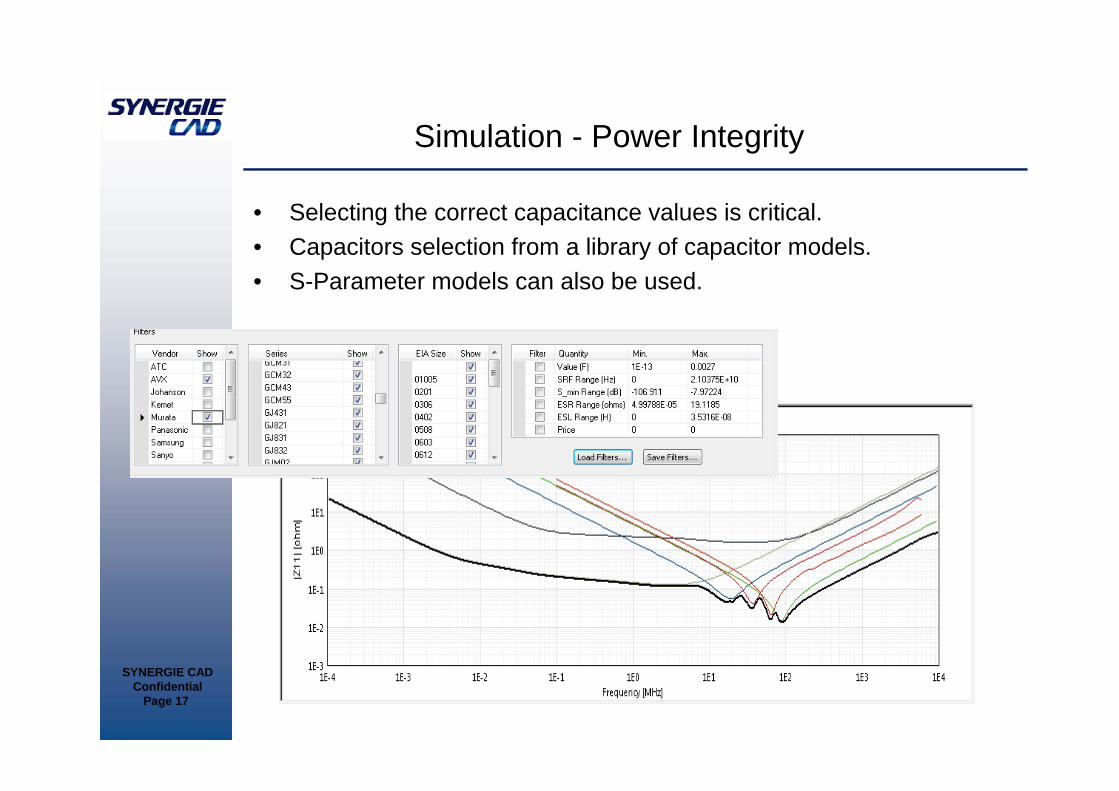
Simulation - Power Integrity
• Selecting the correct capacitance values is critical.• Capacitors selection from a library of capacitor models.• S-Parameter models can also be used.
SYNERGIE CADConfidential
Page 18
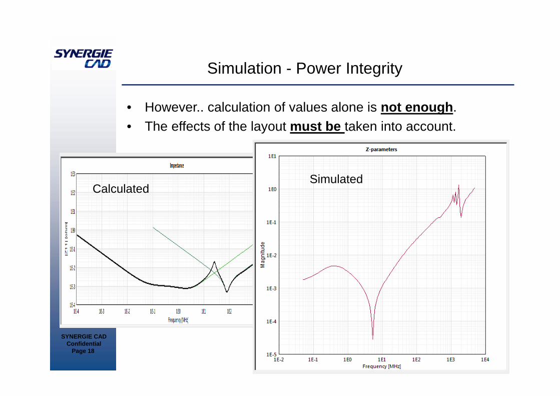
Simulation - Power Integrity
• However.. calculation of values alone is not enough.• The effects of the layout must be taken into account.
CalculatedSimulated
SYNERGIE CADConfidential
Page 19
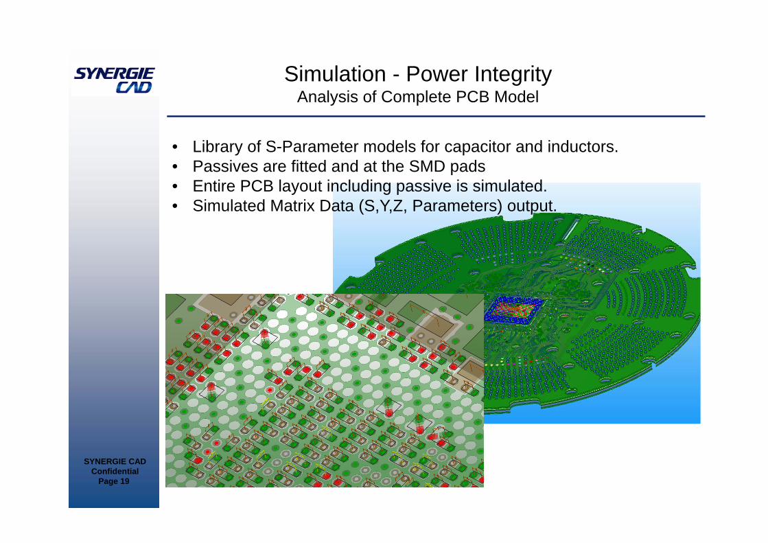
Simulation - Power Integrity Analysis of Complete PCB Model
• Library of S-Parameter models for capacitor and inductors.• Passives are fitted and at the SMD pads• Entire PCB layout including passive is simulated. • Simulated Matrix Data (S,Y,Z, Parameters) output.

SYNERGIE CADConfidential
Page 20
Simulation - Power Integrity Placement effect on Target Impedance
1KHz 1MHz 100MHz GHz
BulkCapacitors
CeramicCapacitors
Planes
• The effect of the placement and layout must be included in the overall model.
• Optimisation of the placement of components is required to minimise plane resonances.
• Optimisation of capacitor type / placement for the required performance over the desired frequency range.
• Optimisation of the layout to improve performance.– Inductance loops– Via length– Plane impedance
SYNERGIE CADConfidential
Page 21
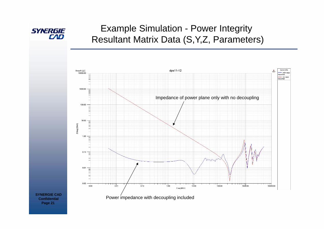
Example Simulation - Power Integrity Resultant Matrix Data (S,Y,Z, Parameters)
Impedance of power plane only with no decoupling
Power impedance with decoupling included
SYNERGIE CADConfidential
Page 22
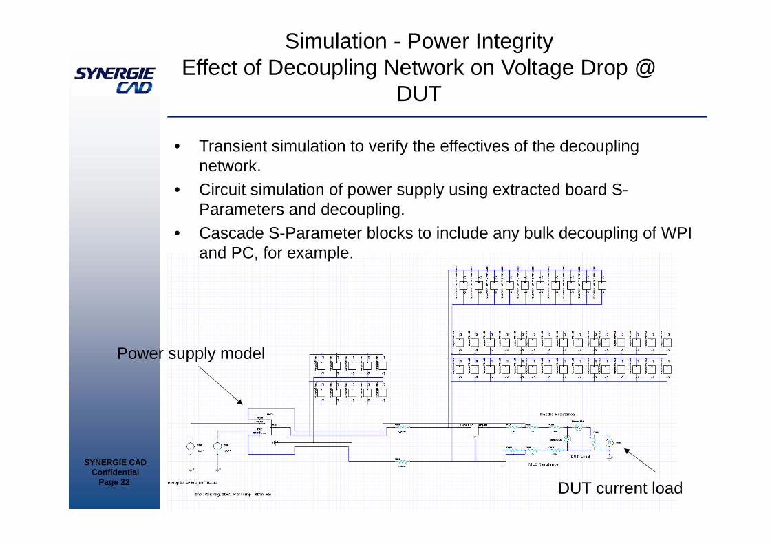
Simulation - Power Integrity Effect of Decoupling Network on Voltage Drop @
DUT
• Transient simulation to verify the effectives of the decoupling network.
• Circuit simulation of power supply using extracted board S-Parameters and decoupling.
• Cascade S-Parameter blocks to include any bulk decoupling of WPI and PC, for example.
Power supply model
DUT current load

SYNERGIE CADConfidential
Page 23
Simulation - Power Integrity Effect of Decoupling Network on Voltage Drop @ DUT (cont.)
• Transient simulation to verify the effectives of the decoupling network.
• Power supply models of the tester hardware provided by the tester manufacturer.
• Simulate and verify the effects of a current transient on the overall network.

SYNERGIE CADConfidential
Page 24
Thank You