simultaneous read/write operations in dual-port sram in
TRANSCRIPT
Application Note AC374
Simultaneous Read-Write Operations in Dual-Port SRAM for Flash-Based cSoCs and FPGAs
IntroductionAs design complexity grows, greater demands are placed upon embedded memory. MicrosemiSmartFusion® customizable system-on-chip (cSoC) and Fusion, IGLOO®, and ProASIC®3 FPGAsprovide the flexibility of true dual-port SRAM blocks. The dual-port configuration has two separate blocks(block A and block B) and corresponding clocks (CLKA and CLKB). This allows the user to perform bothread and write operations on both blocks A and B. However, when performing simultaneous operationsthere may be data collisions and undesired data may be obtained at the output. There are four possiblesimultaneous memory access operations occurring in the same clock cycle at the same address in adual-port SRAM: read-write, write-write, read-read, and write-read. While a read-read operation on thesame address is not affected in any way, proper measures need to be taken for the other threeoperations to ensure that no data collision occurs. The intent of this application note is to discuss these three operations in detail. This application noteconsists of three chapters. "Chapter 1: IGLOO and ProASIC3L/EL Series FPGAs" – The first chapter describes the simultaneousread-write operations of dual-port SRAM in IGLOO series FPGAs and ProASIC3L/EL series devices."Chapter 2: ProASIC3 Series FPGAs " – The second chapter describes the simultaneous read-writeoperations of dual-port SRAM in ProASIC3 series FPGAs. "Chapter 3: SmartFusion cSoCs and Fusion FPGAs" – The third chapter describes the simultaneousread-write operations of dual-port SRAM in SmartFusion and Fusion devices.
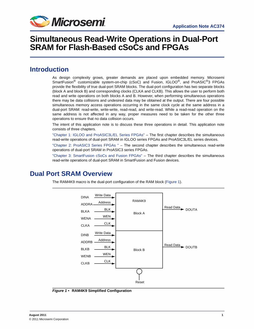
Dual Port SRAM OverviewThe RAM4K9 macro is the dual-port configuration of the RAM block (Figure 1).
Figure 1 • RAM4K9 Simplified Configuration
DOUTA
DOUTB
Write DataDINAAddressADDRA
BLKBLKAWENWENACLKCLKA
Read Data
Write DataDINBAddressADDRB
BLKBLKBWENWENBCLKCLKB
Read Data
RAM4K9
Block A
Block B
Reset
August 2011 1© 2011 Microsemi Corporation

Simultaneous Read-Write Operations in Dual-Port SRAM for Flash-Based cSoCs and FPGAs
The RAM4K9 nomenclature refers to both the deepest possible configuration and the widest possibleconfiguration the dual-port RAM block can assume, and does not denote a possible memory aspect ratio.The RAM block can be configured to the following aspect ratios: 4,096×1, 2,048×2, 1,024×4, and 512×9.RAM4K9 is fully synchronous and has the following features:
• Two ports that allow fully independent reads and writes at different frequencies• Selectable pipelined or nonpipelined read• Active low block enables for each port• Toggle control between read and write mode for each port• Active low asynchronous reset• Pass-through writes data or holds existing data on output. In pass-through mode, the data written
to the write port will immediately appear on the read port.• Designer software will automatically facilitate falling-edge clocks by bubble-pushing the inversion
to previous stages.The SRAM architecture, modes of operation, and signal descriptions for each family can be found in theirrespective user’s guides. Similarly, total embedded SRAM for each device can be found in theirrespective datasheets. Each chapter provides a table with list of supported devices and links to theiruser’s guides and datasheets.
2

Chapter 1: IGLOO and ProASIC3L/EL Series FPGAs
Chapter 1: IGLOO and ProASIC3L/EL Series FPGAsThis chapter describes the simultaneous read-write operations of dual-port SRAM in IGLOO seriesFPGAs and ProASIC3/EL series devices. This chapter is applicable only to listed devices in Table 1.
Simultaneous Write-Write OperationsSimultaneous write-write is defined as a situation when the two clocks, CLKA and CLKB, turn on veryclose to one another to initiate a write operation on the same address of the RAM.The behavior in a write-write situation depends on what occurs at the negative or closing edge of theclock. The word line—access to SRAM cell is enabled by word line—is asserted at the positive edge ofthe clock and deasserted at the negative edge. This means that once a write operation is commencedwith port A, the content of the memory cannot be overwritten with port B until the clock signal (or wordline) goes low. Therefore, a small delay is required between the negative edges of CLKA and CLKB inorder to successfully perform a simultaneous write. The various behaviors are described in Table 2. Eachcase is discussed in detail in the following sections.
Table 1 • Supported Devices in Chapter 1
Series Datasheet User’s Guide
IGLOO IGLOO Low Power Flash FPGAs IGLOO FPGA Fabric User’s Guide
IGLOOe Low Power Flash FPGAs IGLOOe FPGA Fabric User’s Guide
IGLOO nano Low Power Flash FPGAs IGLOO nano FPGA Fabric User’s Guide
IGLOO PLUS Low Power Flash FPGAs IGLOO PLUS FPGA Fabric User’s Guide
ProASIC3 ProASIC3L Low Power Flash FPGAs ProASIC3L FPGA Fabric User’s Guide
Radiation-Tolerant ProASIC3 Low PowerSpaceflight Flash FPGAs
RT ProASIC3EL FPGA Fabric User’s Guide
Military ProASIC3/EL Low Power FlashFPGAs (A3PE600L and A3PE3000L)
Military ProASIC3EL FPGA Fabric User’sGuide (A3PE600L and A3PE3000L)
Table 2 • List of Simultaneous Write-Write Scenarios
Case DescriptionOutput When Data is Read
After Write-Write Operations
1 Simultaneous clock on rising edge, CLKB falls before CLKA Data from CLKA
2 Simultaneous clock on rising edge, CLKB falls after CLKA Data from CLKB
3 CLKB rises after CLKA, CLKB falls before CLKA Data from CLKA
4 CLKB rises after CLKA, CLKB falls after CLKA Data from CLKB
5 CLKB rises when CLKA falls, CLKB falls after CLKA Data from CLKB
6 CLKB rises after CLKA falls, CLKB falls after CLKA falls Data from CLKB
3
Simultaneous Read-Write Operations in Dual-Port SRAM for Flash-Based cSoCs and FPGAs
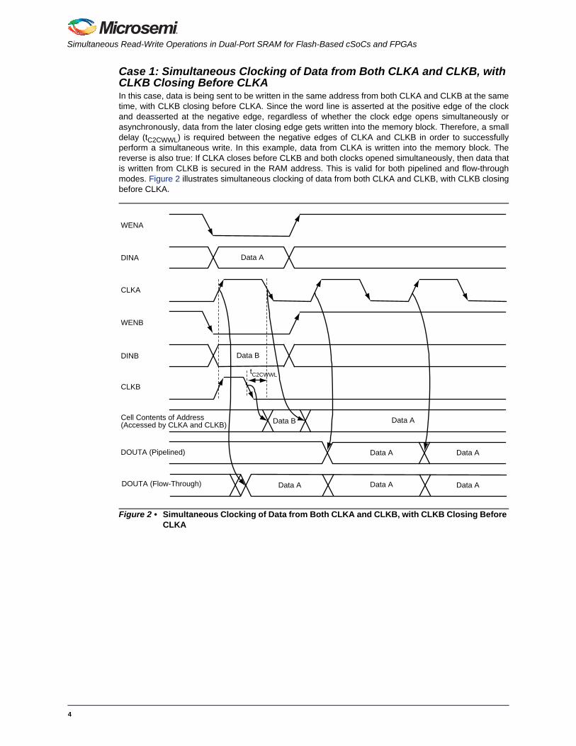
Case 1: Simultaneous Clocking of Data from Both CLKA and CLKB, with CLKB Closing Before CLKAIn this case, data is being sent to be written in the same address from both CLKA and CLKB at the sametime, with CLKB closing before CLKA. Since the word line is asserted at the positive edge of the clockand deasserted at the negative edge, regardless of whether the clock edge opens simultaneously orasynchronously, data from the later closing edge gets written into the memory block. Therefore, a smalldelay (tC2CWWL) is required between the negative edges of CLKA and CLKB in order to successfullyperform a simultaneous write. In this example, data from CLKA is written into the memory block. Thereverse is also true: If CLKA closes before CLKB and both clocks opened simultaneously, then data thatis written from CLKB is secured in the RAM address. This is valid for both pipelined and flow-throughmodes. Figure 2 illustrates simultaneous clocking of data from both CLKA and CLKB, with CLKB closingbefore CLKA.
Figure 2 • Simultaneous Clocking of Data from Both CLKA and CLKB, with CLKB Closing Before CLKA
WENA
DINA Data A
CLKA
WENB
DINB Data B
CLKB
Cell Contents of Address (Accessed by CLKA and CLKB)
DOUTA (Pipelined)
tC2CWWL
DOUTA (Flow-Through)
Data B Data A
Data A Data A
Data AData AData A
4
Chapter 1: IGLOO and ProASIC3L/EL Series FPGAs
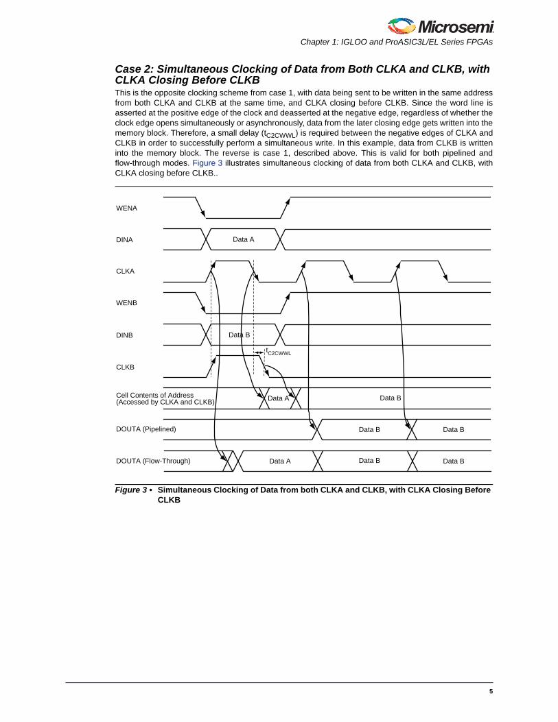
Case 2: Simultaneous Clocking of Data from Both CLKA and CLKB, with CLKA Closing Before CLKBThis is the opposite clocking scheme from case 1, with data being sent to be written in the same addressfrom both CLKA and CLKB at the same time, and CLKA closing before CLKB. Since the word line isasserted at the positive edge of the clock and deasserted at the negative edge, regardless of whether theclock edge opens simultaneously or asynchronously, data from the later closing edge gets written into thememory block. Therefore, a small delay (tC2CWWL) is required between the negative edges of CLKA andCLKB in order to successfully perform a simultaneous write. In this example, data from CLKB is writteninto the memory block. The reverse is case 1, described above. This is valid for both pipelined andflow-through modes. Figure 3 illustrates simultaneous clocking of data from both CLKA and CLKB, withCLKA closing before CLKB..
Figure 3 • Simultaneous Clocking of Data from both CLKA and CLKB, with CLKA Closing Before CLKB
WENA
DINA Data A
CLKA
WENB
DINB Data B
CLKB
Cell Contents of Address (Accessed by CLKA and CLKB)
DOUTA (Pipelined)
tC2CWWL
DOUTA (Flow-Through)
Data A Data B
Data B Data B
Data BData BData A
5
Simultaneous Read-Write Operations in Dual-Port SRAM for Flash-Based cSoCs and FPGAs
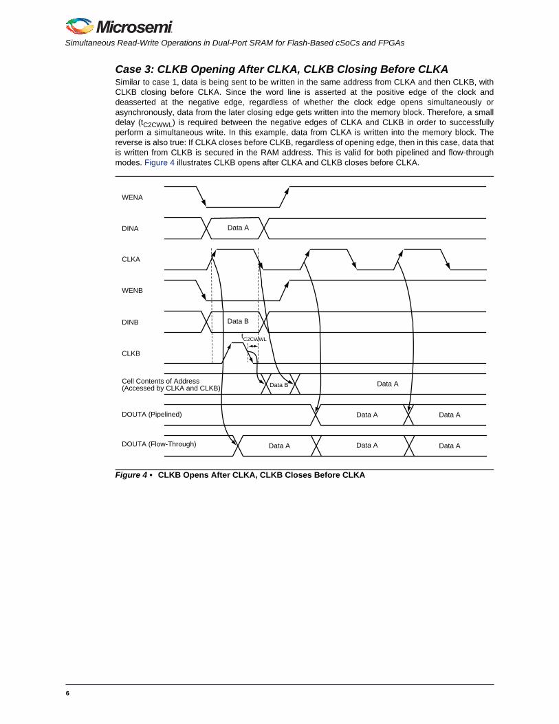
Case 3: CLKB Opening After CLKA, CLKB Closing Before CLKASimilar to case 1, data is being sent to be written in the same address from CLKA and then CLKB, withCLKB closing before CLKA. Since the word line is asserted at the positive edge of the clock anddeasserted at the negative edge, regardless of whether the clock edge opens simultaneously orasynchronously, data from the later closing edge gets written into the memory block. Therefore, a smalldelay (tC2CWWL) is required between the negative edges of CLKA and CLKB in order to successfullyperform a simultaneous write. In this example, data from CLKA is written into the memory block. Thereverse is also true: If CLKA closes before CLKB, regardless of opening edge, then in this case, data thatis written from CLKB is secured in the RAM address. This is valid for both pipelined and flow-throughmodes. Figure 4 illustrates CLKB opens after CLKA and CLKB closes before CLKA.
Figure 4 • CLKB Opens After CLKA, CLKB Closes Before CLKA
WENA
DINA Data A
CLKA
WENB
DINB Data B
CLKB
Cell Contents of Address (Accessed by CLKA and CLKB)
DOUTA (Pipelined)
tC2CWWL
DOUTA (Flow-Through)
Data B Data A
Data A Data A
Data AData AData A
6
Chapter 1: IGLOO and ProASIC3L/EL Series FPGAs
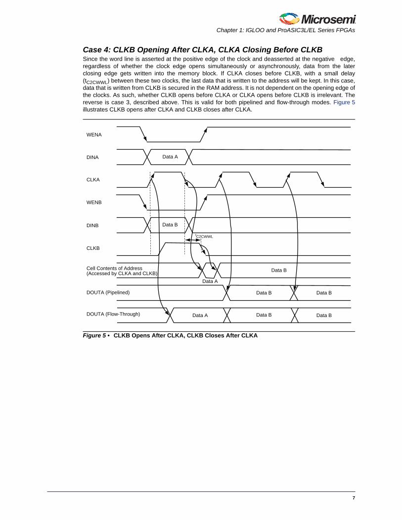
Case 4: CLKB Opening After CLKA, CLKA Closing Before CLKBSince the word line is asserted at the positive edge of the clock and deasserted at the negative edge,regardless of whether the clock edge opens simultaneously or asynchronously, data from the laterclosing edge gets written into the memory block. If CLKA closes before CLKB, with a small delay(tC2CWWL) between these two clocks, the last data that is written to the address will be kept. In this case,data that is written from CLKB is secured in the RAM address. It is not dependent on the opening edge ofthe clocks. As such, whether CLKB opens before CLKA or CLKA opens before CLKB is irrelevant. Thereverse is case 3, described above. This is valid for both pipelined and flow-through modes. Figure 5illustrates CLKB opens after CLKA and CLKB closes after CLKA.
Figure 5 • CLKB Opens After CLKA, CLKB Closes After CLKA
WENA
DINA Data A
CLKA
WENB
DINB Data B
CLKB
Cell Contents of Address (Accessed by CLKA and CLKB)
DOUTA (Pipelined)
tC2CWWL
DOUTA (Flow-Through)
Data A
Data B
Data B Data B
Data BData BData A
7

Simultaneous Read-Write Operations in Dual-Port SRAM for Flash-Based cSoCs and FPGAs
Case 5: CLKB Opening When CLKA Closes, CLKB Closes After CLKA ClosesThere is actually no collision in this case; it is normal operation. Thus, there is no additional constraintunder this condition. Since data written by CLKA is completed before data written by CLKB isinstantiated, no collisions occur. By intuition, the last data written to the address is stored. In thisexample, the data written from CLKB is stored in the memory. As a result, in the next cycle where thedata is read, data B is read from the memory. The reverse is also true: if data written by CLKA precedesdata written by CLKB, data that is written from CLKA is secured into the memory. This is valid for bothpipelined and flow-through modes. Figure 6 illustrates CLKB opens when CLKA closes and CLKB closesafter CLKA closes.
Figure 6 • CLKB Opens When CLKA Closes; CLKB Closes After CLKA Closes
WENA
DINA Data A
CLKA
WENB
DINB Data B
CLKB
Cell Contents of Address (Accessed by CLKA and CLKB)
DOUTA (Pipelined)
DOUTA (Flow-Through)
Data A Data B
Data B
Data BData A
8
Chapter 1: IGLOO and ProASIC3L/EL Series FPGAs
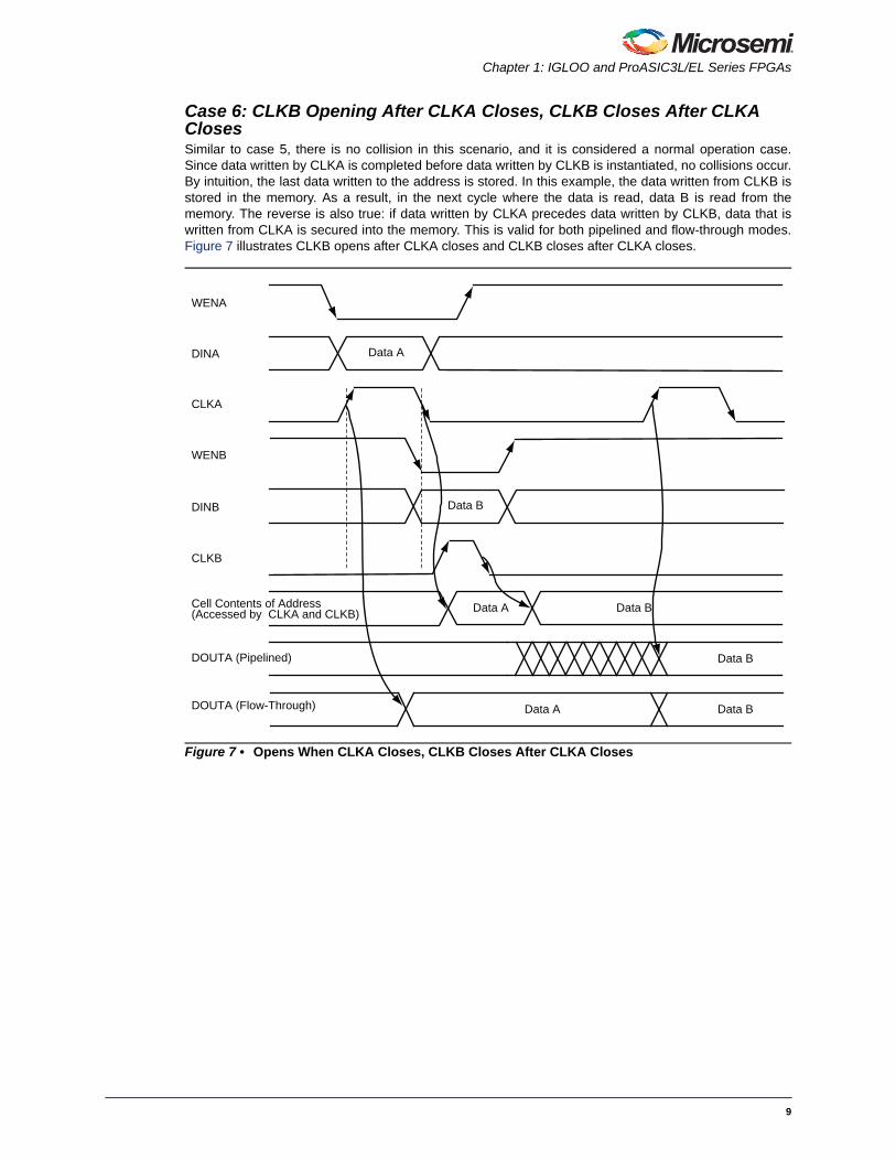
Case 6: CLKB Opening After CLKA Closes, CLKB Closes After CLKA ClosesSimilar to case 5, there is no collision in this scenario, and it is considered a normal operation case.Since data written by CLKA is completed before data written by CLKB is instantiated, no collisions occur.By intuition, the last data written to the address is stored. In this example, the data written from CLKB isstored in the memory. As a result, in the next cycle where the data is read, data B is read from thememory. The reverse is also true: if data written by CLKA precedes data written by CLKB, data that iswritten from CLKA is secured into the memory. This is valid for both pipelined and flow-through modes.Figure 7 illustrates CLKB opens after CLKA closes and CLKB closes after CLKA closes.
Figure 7 • Opens When CLKA Closes, CLKB Closes After CLKA Closes
WENA
DINA Data A
CLKA
WENB
DINB Data B
CLKB
Cell Contents of Address (Accessed by CLKA and CLKB)
DOUTA (Pipelined)
DOUTA (Flow-Through)
Data A Data B
Data B
Data BData A
9

Simultaneous Read-Write Operations in Dual-Port SRAM for Flash-Based cSoCs and FPGAs
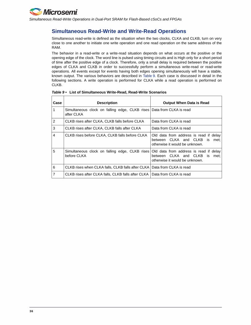
Simultaneous Read-Write and Write-Read OperationsSimultaneous read-write is defined as the situation when the two clocks, CLKA and CLKB, turn on veryclose to one another to initiate one write operation and one read operation on the same address of theRAM.The behavior in a read-write or a write-read situation depends on what occurs at the positive or theopening edge of the clock. Since it takes time for the write operation to occur and also the read operation,a small delay is required between the positive edges of CLKA and CLKB in order to successfully performa simultaneous write-read or read-write operations. All events except for events having both edgesopening simultaneously will have a stable, known output. A write operation is performed for CLKA while aread operation is performed on CLKB. The various behaviors are described in Table 3. Each case will bediscussed in detail in the following sections.
Table 3 • List of Simultaneous Write-Read, Read-Write Scenarios
Case Description Output When Data is Read
1 Simultaneous clock on falling edge, CLKB risesafter CLKA
Data from CLKA is read
2 CLKB rises after CLKA, CLKB falls before CLKA Data from CLKA is read
3 CLKB rises after CLKA, CLKB falls after CLKA Data from CLKA is read
4 CLKB rises before CLKA, CLKB falls before CLKA Old data from address is read if delaybetween CLKA and CLKB is met, else itwould be unknown
5 Simultaneous clock on falling edge, CLKB risesbefore CLKA
Old data from address is read if delaybetween CLKA and CLKB is met;otherwise it would be unknown
6 CLKB rises when CLKA falls, CLKB falls after CLKA Data from CLKA is read
7 CLKB rises after CLKA falls, CLKB falls after CLKA Data from CLKA is read
10
Chapter 1: IGLOO and ProASIC3L/EL Series FPGAs
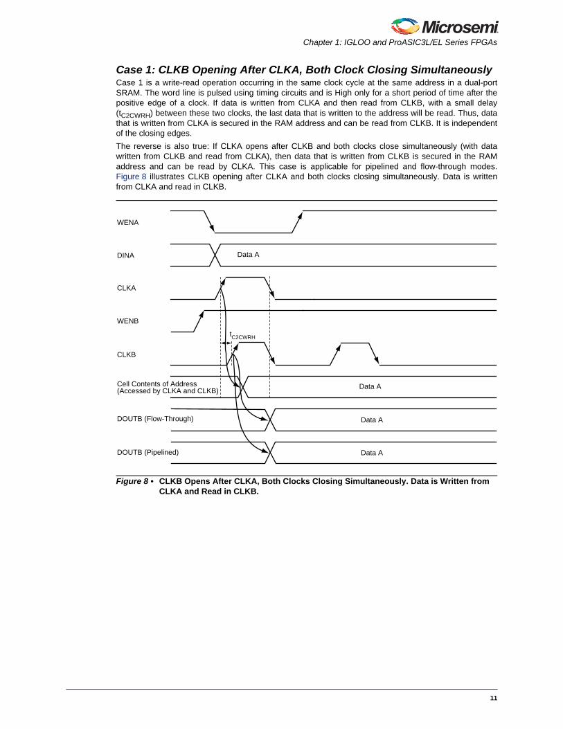
Case 1: CLKB Opening After CLKA, Both Clock Closing SimultaneouslyCase 1 is a write-read operation occurring in the same clock cycle at the same address in a dual-portSRAM. The word line is pulsed using timing circuits and is High only for a short period of time after thepositive edge of a clock. If data is written from CLKA and then read from CLKB, with a small delay(tC2CWRH) between these two clocks, the last data that is written to the address will be read. Thus, datathat is written from CLKA is secured in the RAM address and can be read from CLKB. It is independentof the closing edges. The reverse is also true: If CLKA opens after CLKB and both clocks close simultaneously (with datawritten from CLKB and read from CLKA), then data that is written from CLKB is secured in the RAMaddress and can be read by CLKA. This case is applicable for pipelined and flow-through modes.Figure 8 illustrates CLKB opening after CLKA and both clocks closing simultaneously. Data is writtenfrom CLKA and read in CLKB.
Figure 8 • CLKB Opens After CLKA, Both Clocks Closing Simultaneously. Data is Written from CLKA and Read in CLKB.
WENA
DINA Data A
CLKA
WENB
CLKB
Cell Contents of Address (Accessed by CLKA and CLKB)
DOUTB (Flow-Through)
Data A
tC2CWRH
DOUTB (Pipelined)
Data A
Data A
11

Simultaneous Read-Write Operations in Dual-Port SRAM for Flash-Based cSoCs and FPGAs
Case 2: CLKB Opening After CLKA, CLKB Closes Before CLKASimilar to case 1, case 2 is a write-read operation occurring in the same clock cycle at the same addressin a dual-port SRAM. The word line is pulsed using timing circuits and is High only for a short period oftime after the positive edge of a clock. If data is written from CLKA and then read from CLKB, with a smalldelay (tC2CWRH) between these two clocks, the last data that is written to the address will be read. Thus,data that is written from CLKA is secured in the RAM address and can be read from CLKB. The ability ofthe data to be read accurately is independent of the closing edges, regardless of whether the clockedges close simultaneously or asynchronously.The reverse is also true: If CLKA opens after CLKB and CLKA closes before CLKB (with data writtenfrom CLKB and read from CLKA), then data that is written from CLKB is secured in the RAM address andcan be read by CLKA. This case is applicable for pipelined and flow-through modes. Figure 9 illustratesCLKB opens after CLKA and CLKB closes before CLKA. Data is written from CLKA and read in CLKB.
Figure 9 • CLKB Opens After CLKA, CLKB Closes Before CLKA. Data is Written from CLKA and Read in CLKB.
WENA
DINA Data A
CLKA
WENB
CLKB
Cell Contents of Address (Accessed by CLKA and CLKB)
DOUTB (Flow-Through)
Data A
tC2CWRH
DOUTB (Pipelined)
Data A
Data A
12
Chapter 1: IGLOO and ProASIC3L/EL Series FPGAs
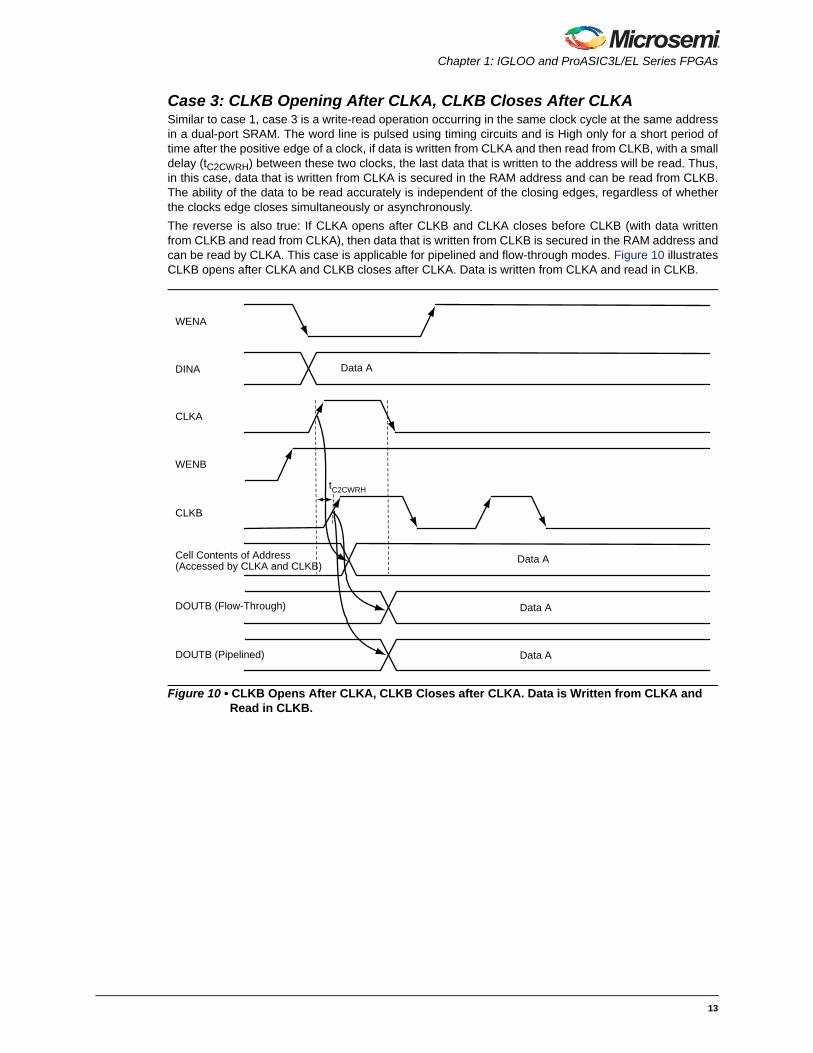
Case 3: CLKB Opening After CLKA, CLKB Closes After CLKASimilar to case 1, case 3 is a write-read operation occurring in the same clock cycle at the same addressin a dual-port SRAM. The word line is pulsed using timing circuits and is High only for a short period oftime after the positive edge of a clock, if data is written from CLKA and then read from CLKB, with a smalldelay (tC2CWRH) between these two clocks, the last data that is written to the address will be read. Thus,in this case, data that is written from CLKA is secured in the RAM address and can be read from CLKB.The ability of the data to be read accurately is independent of the closing edges, regardless of whetherthe clocks edge closes simultaneously or asynchronously.The reverse is also true: If CLKA opens after CLKB and CLKA closes before CLKB (with data writtenfrom CLKB and read from CLKA), then data that is written from CLKB is secured in the RAM address andcan be read by CLKA. This case is applicable for pipelined and flow-through modes. Figure 10 illustratesCLKB opens after CLKA and CLKB closes after CLKA. Data is written from CLKA and read in CLKB.
Figure 10 • CLKB Opens After CLKA, CLKB Closes after CLKA. Data is Written from CLKA and Read in CLKB.
WENA
DINA Data A
CLKA
WENB
CLKB
Cell Contents of Address (Accessed by CLKA and CLKB)
DOUTB (Flow-Through)
Data A
tC2CWRH
DOUTB (Pipelined)
Data A
Data A
13

Simultaneous Read-Write Operations in Dual-Port SRAM for Flash-Based cSoCs and FPGAs
Case 4: CLKB Opening Before CLKA Opens, CLKB Closes Before CLKA ClosesIn this case, it is a read-write operation rather than a write-read operation. Since write and readoperations cannot occur instantaneously, a small delay occurs between the read and write operations(tC2CRWH). If this delay is met, the old data from the address is read by CLKB before new data overwritesthe old data by CLKA. The reverse is also true: if data being read by CLKA precedes data written byCLKB, the old data in the address is read before new data from CLKB is secured into the memory. Thisis valid for both pipelined and flow-through modes. Figure 11 illustrates CLKB opens before CLKA opensand CLKB before CLKA closes. Data is written from CLKA and read in CLKB.
Figure 11 • CLKB Opens Before CLKA Opens, CLKB Closes Before CLKA Closes. Data is Written from CLKA and Read in CLKB.
WENA
DINA Data A
CLKA
WENB
CLKB
Cell Contents of Address (Accessed by CLKA and CLKB) Data A
DOUTB (Flow-Through) Data A
tC2CRWH
Old Data
Old Data
DOUTB (Pipelined) Data AOld Data
14

Chapter 1: IGLOO and ProASIC3L/EL Series FPGAs
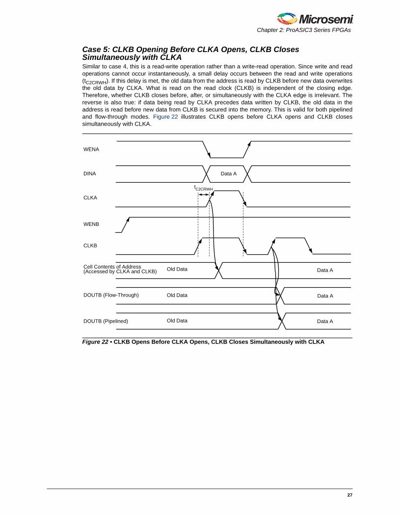
Case 5: CLKB Opening Before CLKA Opens, CLKB Closes Simultaneously with CLKASimilar to case 4, this is a read-write operation rather than a write-read operation. Since write and readoperations cannot occur instantaneously, a small delay occurs between the read and write operations(tC2CRWH). If this delay is met, the old data from the address is read by CLKB before new data overwritesthe old data by CLKA. What is read on the read clock (CLKB) is independent of the closing edge.Therefore, whether CLKB closes before, after, or simultaneously with the CLKA edge is irrelevant. Thereverse is also true: if data being read by CLKA precedes data written by CLKB, the old data in theaddress is read before new data from CLKB is secured into the memory. This is valid for both pipelinedand flow-through modes. Figure 12 illustrates CLKB opens before CLKA opens and CLKB closessimultaneously with CLKA. Data is written from CLKA and read in CLKB.
Figure 12 • CLKB Opens Before CLKA Opens, CLKB Closes Simultaneously with CLKA. Data is Written from CLKA and Read in CLKB.
WENA
DINA Data A
CLKA
WENB
CLKB
Cell Contents of Address (Accessed by CLKA and CLKB) Data A
DOUTB (Flow-Through) Data A
tC2CRWH
Old Data
Old Data
DOUTB (Pipelined) Data AOld Data
15

Simultaneous Read-Write Operations in Dual-Port SRAM for Flash-Based cSoCs and FPGAs
Case 6: CLKB Opening when CLKA Closes, CLKB Closes After CLKAThere is no collision in case 6, and it is considered a normal operation case. Thus, there is no additionalconstraint under this condition. Since data written by CLKA is completed before data is read by CLKB, nocollisions occur. By intuition, the last data written to the address is stored and read. In this example, thedata written from CLKA is stored in the memory. As a result, when CLKB opens, the data written byCLKA in the same memory location is read. The reverse is also true: If data written by CLKB precedesdata read by CLKA, data that is written from CLKB is secured into the memory and is read by CLKA. Thisis valid for both pipelined and flow-through modes. Figure 13 illustrates CLKB opens when CLKA closes,CLKB closes after CLKA. Data is written from CLKA and read in CLKB, in pipelined mode.
Figure 13 • CLKB Opens When CLKA Closes; CLKB Closes After CLKA. Data Is Written from CLKA and Read in CLKB, Pipelined Mode.
WENA
DINA Data A
CLKA
WENB
CLKB
Cell Contents of Address (Accessed by CLKA and CLKB)
Data A
DOUTB (Pipelined) Data A
16
Chapter 1: IGLOO and ProASIC3L/EL Series FPGAs
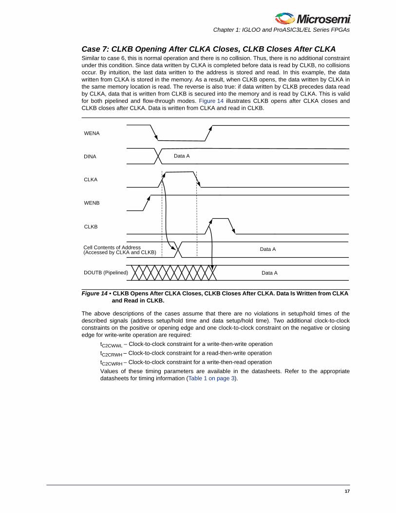
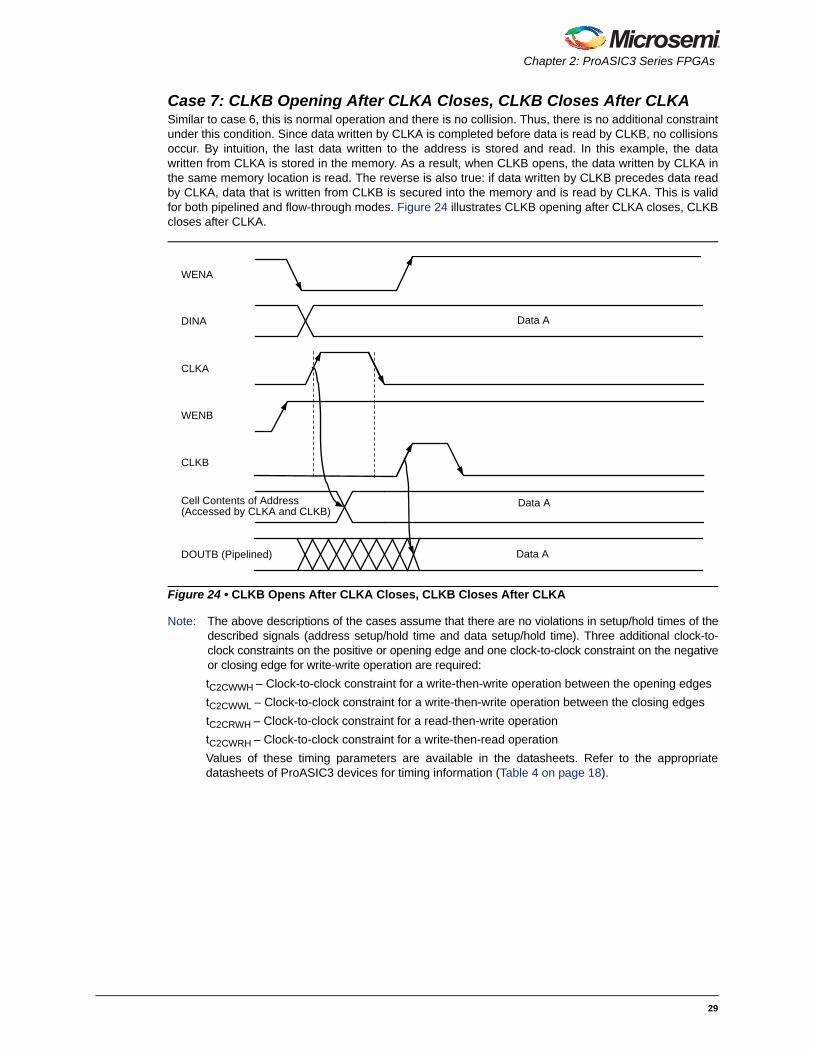
Case 7: CLKB Opening After CLKA Closes, CLKB Closes After CLKASimilar to case 6, this is normal operation and there is no collision. Thus, there is no additional constraintunder this condition. Since data written by CLKA is completed before data is read by CLKB, no collisionsoccur. By intuition, the last data written to the address is stored and read. In this example, the datawritten from CLKA is stored in the memory. As a result, when CLKB opens, the data written by CLKA inthe same memory location is read. The reverse is also true: if data written by CLKB precedes data readby CLKA, data that is written from CLKB is secured into the memory and is read by CLKA. This is validfor both pipelined and flow-through modes. Figure 14 illustrates CLKB opens after CLKA closes andCLKB closes after CLKA. Data is written from CLKA and read in CLKB.
The above descriptions of the cases assume that there are no violations in setup/hold times of thedescribed signals (address setup/hold time and data setup/hold time). Two additional clock-to-clockconstraints on the positive or opening edge and one clock-to-clock constraint on the negative or closingedge for write-write operation are required:
tC2CWWL – Clock-to-clock constraint for a write-then-write operationtC2CRWH – Clock-to-clock constraint for a read-then-write operationtC2CWRH – Clock-to-clock constraint for a write-then-read operationValues of these timing parameters are available in the datasheets. Refer to the appropriatedatasheets for timing information (Table 1 on page 3).
Figure 14 • CLKB Opens After CLKA Closes, CLKB Closes After CLKA. Data Is Written from CLKA and Read in CLKB.
WENA
DINA
CLKA
WENB
CLKB
Cell Contents of Address (Accessed by CLKA and CLKB)
DOUTB (Pipelined)
Data A
Data A
Data A
17

Simultaneous Read-Write Operations in Dual-Port SRAM for Flash-Based cSoCs and FPGAs
Chapter 2: ProASIC3 Series FPGAs This section describes the simultaneous read-write operations of dual-port SRAM in ProASIC3 seriesFPGAs. This section is applicable only to listed devices in Table 4.
Simultaneous Write-Write OperationsSimultaneous write-write is defined as the situation when the two clocks, CLKA and CLKB, turn on veryclose to one another to initiate a write operation on the same address of the RAM.The behavior in a write-write situation depends on what occurs at both the negative or closing edge ofthe clock and the positive or opening edge of the clock. Therefore, a small delay is required between thenegative edges of CLKA and CLKB as well as the positive edges of CLKA and CLKB in order tosuccessfully perform simultaneous write. In addition, neither clock can fully overlap one another.Example cases are described in Table 5 and discussed further in the next section.
Table 4 • Supported Devices in Chapter 2
Datasheet User’s Guide
ProASIC3 Flash Family FPGAs ProASIC3 FPGA Fabric User’s Guide
ProASIC3E Flash Family FPGAs ProASIC3E FPGA Fabric User’s Guide
ProASIC3 nano Flash FPGAs ProASIC3 nano FPGA Fabric User’s Guide
Military ProASIC3/EL Low Power Flash FPGAs (A3P250 and A3P1000)
Military ProASIC3/EL FPGA Fabric User’s Guide (A3P250 and A3P1000)
Automotive ProASIC3 Flash Family FPGAs Automotive ProASIC3 FPGA Fabric User’s Guide
Table 5 • List of Simultaneous Write-Write Scenarios
Case DescriptionOutput When Data is Read After
Write-Write Operations
1 CLKB rises after CLKA, CLKB falls after CLKA Data from CLKB
2 CLKB rises when CLKA falls, CLKB falls after CLKA Data from CLKB
3 CLKB rises after CLKA falls, CLKB falls after CLKA falls Data from CLKB
18
Chapter 2: ProASIC3 Series FPGAs
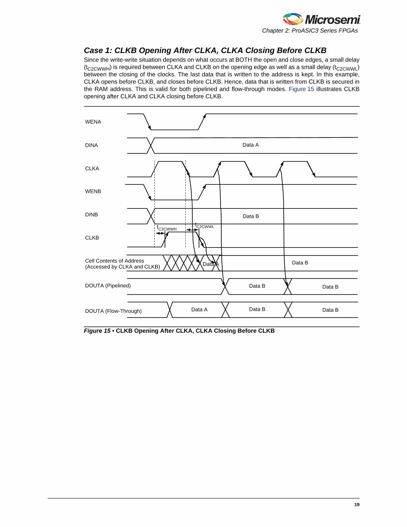
Case 1: CLKB Opening After CLKA, CLKA Closing Before CLKBSince the write-write situation depends on what occurs at BOTH the open and close edges, a small delay(tC2CWWH) is required between CLKA and CLKB on the opening edge as well as a small delay (tC2CWWL)between the closing of the clocks. The last data that is written to the address is kept. In this example,CLKA opens before CLKB, and closes before CLKB. Hence, data that is written from CLKB is secured inthe RAM address. This is valid for both pipelined and flow-through modes. Figure 15 illustrates CLKBopening after CLKA and CLKA closing before CLKB.
Figure 15 • CLKB Opening After CLKA, CLKA Closing Before CLKB
Data A
WENA
DINA
CLKA
WENB
Data BDINB
CLKB
Data B
Data A
Data ACell Contents of Address (Accessed by CLKA and CLKB)
DOUTA (Pipelined)
DOUTA (Flow-Through)
Data BData B
Data B Data B
tC2CWWHtC2CWWL
19

Simultaneous Read-Write Operations in Dual-Port SRAM for Flash-Based cSoCs and FPGAs
Case 2: CLKB Opening When CLKA Closes, CLKB Closes After CLKA ClosesThere is actually no collision in this case; it is normal operation. Thus, there is no additional constraintunder this condition. Since data written by CLKA is completed before data written by CLKB isinstantiated, no collisions occur. By intuition, the last data written to the address is stored. In thisexample, the data written from CLKB is stored in the memory. As a result, in the next cycle where thedata is read, data B is read from the memory. The reverse is also true: if data written by CLKA precedesdata written by CLKB, data that is written from CLKA is secured into the memory. This is valid for bothpipelined and flow-through modes. Figure 16 illustrates CLKB opening when CLKA closes and CLKBclosing after CLKA closes.
Figure 16 • CLKB Opens When CLKA Closes, CLKB Closes After CLKA Closes
Data A
Data B
WENA
DINA
CLKA
WENB
DINB
CLKB
Cell Contents of Address (Accessed by CLKA and CLKB)
DOUTA (Pipelined)
DOUTA (Flow-Through)
Data B
Data B
Data B
Data A
Data A
20

Chapter 2: ProASIC3 Series FPGAs
Case 3: CLKB Opening After CLKA Closes, CLKB Closes After CLKA ClosesSimilar to case 2, there is no collision in this scenario, and it is considered a normal operation case.Since data written by CLKA is completed before data written by CLKB is instantiated, no collisions occur.By intuition, the last data written to the address is stored. In this example, the data written from CLKB isstored in the memory. As a result, in the next cycle where the data is read, data B is read from thememory. The reverse is also true: if data written by CLKA precedes data written by CLKB, data that iswritten from CLKA is secured into the memory. This is valid for both pipelined and flow-through modes.Figure 17 illustrates CLKB opening after CLKA closes, CLKB closes after CLKA closes.
Figure 17 • CLKB Opens After CLKA Closes, CLKB Closes After CLKA Closes
WENA
DINA
CLKA
WENB
DINB
CLKB
Cell Contents of Address (Accessed by CLKA and CLKB)
DOUTA (Pipelined)
DOUTA (Flow-Through)
Data A
Data B
Data A Data B
Data B
Data A Data B
21
Simultaneous Read-Write Operations in Dual-Port SRAM for Flash-Based cSoCs and FPGAs
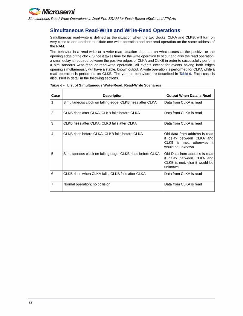
Simultaneous Read-Write and Write-Read OperationsSimultaneous read-write is defined as the situation when the two clocks, CLKA and CLKB, will turn onvery close to one another to initiate one write operation and one read operation on the same address ofthe RAM. The behavior in a read-write or a write-read situation depends on what occurs at the positive or theopening edge of the clock. Since it takes time for the write operation to occur and also the read operation,a small delay is required between the positive edges of CLKA and CLKB in order to successfully performa simultaneous write-read or read-write operation. All events except for events having both edgesopening simultaneously will have a stable, known output. A write operation is performed for CLKA while aread operation is performed on CLKB. The various behaviors are described in Table 6. Each case isdiscussed in detail in the following sections.
Table 6 • List of Simultaneous Write-Read, Read-Write Scenarios
Case Description Output When Data is Read
1 Simultaneous clock on falling edge, CLKB rises after CLKA Data from CLKA is read
2 CLKB rises after CLKA, CLKB falls before CLKA Data from CLKA is read
3 CLKB rises after CLKA, CLKB falls after CLKA Data from CLKA is read
4 CLKB rises before CLKA, CLKB falls before CLKA Old data from address is readif delay between CLKA andCLKB is met; otherwise itwould be unknown
5 Simultaneous clock on falling edge, CLKB rises before CLKA Old Data from address is readif delay between CLKA andCLKB is met, else it would beunknown
6 CLKB rises when CLKA falls, CLKB falls after CLKA Data from CLKA is read
7 Normal operation; no collision Data from CLKA is read
22
Chapter 2: ProASIC3 Series FPGAs
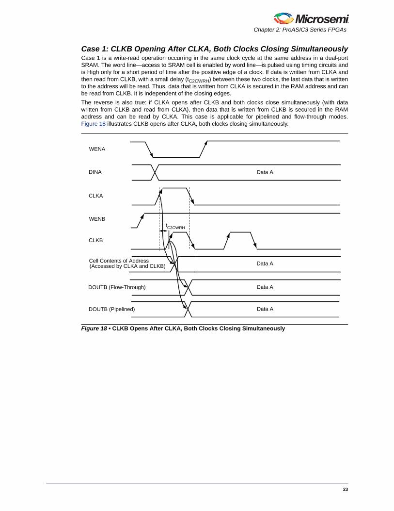
Case 1: CLKB Opening After CLKA, Both Clocks Closing SimultaneouslyCase 1 is a write-read operation occurring in the same clock cycle at the same address in a dual-portSRAM. The word line—access to SRAM cell is enabled by word line—is pulsed using timing circuits andis High only for a short period of time after the positive edge of a clock. If data is written from CLKA andthen read from CLKB, with a small delay (tC2CWRH) between these two clocks, the last data that is writtento the address will be read. Thus, data that is written from CLKA is secured in the RAM address and canbe read from CLKB. It is independent of the closing edges. The reverse is also true: if CLKA opens after CLKB and both clocks close simultaneously (with datawritten from CLKB and read from CLKA), then data that is written from CLKB is secured in the RAMaddress and can be read by CLKA. This case is applicable for pipelined and flow-through modes.Figure 18 illustrates CLKB opens after CLKA, both clocks closing simultaneously.
Figure 18 • CLKB Opens After CLKA, Both Clocks Closing Simultaneously
Data ADINA
CLKA
CLKB
Data A
Data A
Data A
WENB
WENA
Cell Contents of Address (Accessed by CLKA and CLKB)
DOUTB (Pipelined)
DOUTB (Flow-Through)
tC2CWRH
23

Simultaneous Read-Write Operations in Dual-Port SRAM for Flash-Based cSoCs and FPGAs
Case 2: CLKB Opening After CLKA, CLKB Closes Before CLKASimilar to case 1, case 2 is a write-read operation occurring in the same clock cycle at the same addressin a dual-port SRAM. The word line is pulsed using timing circuits and is High only for a short period oftime after the positive edge of a clock. If data is written from CLKA and then read from CLKB, with a smalldelay (tC2CWRH) between these two clocks, the last data that is written to the address will be read. Thus,data that is written from CLKA is secured in the RAM address and can be read from CLKB. The ability ofthe data to be read accurately is independent of the closing edges, regardless of whether the clockedges close simultaneously or asynchronously.The reverse is also true: If CLKA opens after CLKB and CLKA closes before CLKB (with data writtenfrom CLKB and read from CLKA), then data that is written from CLKB is secured in the RAM address andcan be read by CLKA. This case is applicable for pipelined and flow-through modes. Figure 19 illustratesCLKB opens after CLKA and CLKB closes before CLKA.
Figure 19 • CLKB Opens After CLKA, CLKB Closes Before CLKA
DINA Data A
CLKA
CLKB
Data A
Data A
Data A
WENB
WENA
Cell Contents of Address (Accessed by CLKA and CLKB)
DOUTB (Flow-Through)
DOUTB (Pipelined)
tC2CWRH
24

Chapter 2: ProASIC3 Series FPGAs
Case 3: CLKB Opening After CLKA, CLKB Closes After CLKASimilar to case 1, case 3 is a write-read operation occurring in the same clock cycle at the same addressin a dual-port SRAM. The word line is pulsed using timing circuits and is High only for a short period oftime after the positive edge of a clock. If data is written from CLKA and then read from CLKB, with a smalldelay (tC2CWRH) between these two clocks, the last data that is written to the address will be read. Thus,data that is written from CLKA is secured in the RAM address and can be read from CLKB. The ability ofthe data to be read accurately is independent of the closing edges, regardless of whether the clockedges close simultaneously or asynchronously.The reverse is also true: if CLKA opens after CLKB and CLKA closes before CLKB (with data writtenfrom CLKB and read from CLKA), then data that is written from CLKB is secured in the RAM address andcan be read by CLKA. This case is applicable for pipelined and flow-through modes. Figure 20 illustratesCLKB opens after CLKA, CLKB closes after CLKA.
Figure 20 • CLKB Opens After CLKA, CLKB Closes After CLKA
DINA
CLKA
CLKB
WENB
WENA
Data A
Data A
Data A
Data A
Cell Contents of Address (Accessed by CLKA and CLKB)
DOUTB (Flow-Through)
DOUTB (Pipelined)
tC2CWRH
25

Simultaneous Read-Write Operations in Dual-Port SRAM for Flash-Based cSoCs and FPGAs
Case 4: CLKB Opening Before CLKA Opens, CLKB Closes Before CLKA ClosesIn this case, it is a read-write operation rather than a write-read operation. Since write and readoperations cannot occur instantaneously, a small delay occurs between the read and write operations(tC2CRWH). If this delay is met, the old data from the address is read by CLKB before new data overwritesthe old data by CLKA. The reverse is also true: if data being read by CLKA precedes data written byCLKB, the old data in the address is read before new data from CLKB is secured into the memory. This isvalid for both pipelined and flow-through modes. Figure 21 illustrates CLKB opens before CLKA opensand CLKB closes before CLKA closes.
Figure 21 • CLKB Opens Before CLKA Opens, CLKB Closes Before CLKA Closes
Data ADINA
CLKA
CLKB
Old Data Data A
Old Data Data A
WENA
Data A
WENB
Old Data
Cell Contents of Address (Accessed by CLKA and CLKB)
DOUTB (Flow-Through)
DOUTB (Pipelined)
tC2CRWH
26
Chapter 2: ProASIC3 Series FPGAs
Case 5: CLKB Opening Before CLKA Opens, CLKB Closes Simultaneously with CLKASimilar to case 4, this is a read-write operation rather than a write-read operation. Since write and readoperations cannot occur instantaneously, a small delay occurs between the read and write operations(tC2CRWH). If this delay is met, the old data from the address is read by CLKB before new data overwritesthe old data by CLKA. What is read on the read clock (CLKB) is independent of the closing edge.Therefore, whether CLKB closes before, after, or simultaneously with the CLKA edge is irrelevant. Thereverse is also true: if data being read by CLKA precedes data written by CLKB, the old data in theaddress is read before new data from CLKB is secured into the memory. This is valid for both pipelinedand flow-through modes. Figure 22 illustrates CLKB opens before CLKA opens and CLKB closessimultaneously with CLKA.
Figure 22 • CLKB Opens Before CLKA Opens, CLKB Closes Simultaneously with CLKA
Data ADINA
CLKA
CLKB
WENA
WENB
Cell Contents of Address (Accessed by CLKA and CLKB)
DOUTB (Flow-Through)
DOUTB (Pipelined)
Old Data
Old Data
Old Data
Data A
Data A
Data A
tC2CRWH
27

Simultaneous Read-Write Operations in Dual-Port SRAM for Flash-Based cSoCs and FPGAs
Case 6: CLKB Opening When CLKA Closes, CLKB Closes After CLKAThere is no collision in case 6; it is considered a normal operation case. Thus, there is no additionalconstraint under this condition. Since data written by CLKA is completed before data is read by CLKB, nocollisions occur. By intuition, the last data written to the address is stored and read. In this example, thedata written from CLKA is stored in the memory. As a result, when CLKB opens, the data written byCLKA in the same memory location is read. The reverse is also true: if data written by CLKB precedesdata read by CLKA, data that is written from CLKB is secured into the memory and is read by CLKA. Thisis valid for both pipelined and flow-through modes. Figure 23 illustrates CLKB opening when CLKAcloses, CLKB closes after CLKA.
Figure 23 • CLKB Opens When CLKA Closes, CLKB Closes After CLKA
DINA
CLKA
CLKB
WENA
WENB
Cell Contents of Address (Accessed by CLKA and CLKB)
DOUTB (Pipelined)
Data A
Data A
Data A
28
Chapter 2: ProASIC3 Series FPGAs
Case 7: CLKB Opening After CLKA Closes, CLKB Closes After CLKASimilar to case 6, this is normal operation and there is no collision. Thus, there is no additional constraintunder this condition. Since data written by CLKA is completed before data is read by CLKB, no collisionsoccur. By intuition, the last data written to the address is stored and read. In this example, the datawritten from CLKA is stored in the memory. As a result, when CLKB opens, the data written by CLKA inthe same memory location is read. The reverse is also true: if data written by CLKB precedes data readby CLKA, data that is written from CLKB is secured into the memory and is read by CLKA. This is validfor both pipelined and flow-through modes. Figure 24 illustrates CLKB opening after CLKA closes, CLKBcloses after CLKA.
Note: The above descriptions of the cases assume that there are no violations in setup/hold times of thedescribed signals (address setup/hold time and data setup/hold time). Three additional clock-to-clock constraints on the positive or opening edge and one clock-to-clock constraint on the negativeor closing edge for write-write operation are required:tC2CWWH – Clock-to-clock constraint for a write-then-write operation between the opening edgestC2CWWL – Clock-to-clock constraint for a write-then-write operation between the closing edgestC2CRWH – Clock-to-clock constraint for a read-then-write operationtC2CWRH – Clock-to-clock constraint for a write-then-read operationValues of these timing parameters are available in the datasheets. Refer to the appropriatedatasheets of ProASIC3 devices for timing information (Table 4 on page 18).
Figure 24 • CLKB Opens After CLKA Closes, CLKB Closes After CLKA
DINA
CLKA
CLKB
WENA
WENB
Cell Contents of Address (Accessed by CLKA and CLKB)
DOUTB (Pipelined)
Data A
Data A
Data A
29

Simultaneous Read-Write Operations in Dual-Port SRAM for Flash-Based cSoCs and FPGAs
Chapter 3: SmartFusion cSoCs and Fusion FPGAsThis section describes the simultaneous read-write operations of dual-port SRAM in SmartFusion andFusion devices. This section is applicable only to listed devices in Table 7.
Simultaneous Write-Write OperationsSimultaneous write-write is defined as the situation when the two clocks, CLKA and CLKB, turn on veryclose to one another to initiate a write operation on the same address of the RAM.The behavior in a write-write situation depends on what occurs at the positive or the opening edge of theclock. The word line—access to SRAM cell is enabled by word line—is pulsed using timing circuits and isHigh only for a short period of time after the positive edge of a clock. Therefore, only a small delay isrequired between the positive edges of CLKA and CLKB in order to successfully perform a simultaneouswrite. The various behaviors are described in Table 8. Each case is discussed in detail in the followingsections.
Table 7 • Supported Devices in Chapter 3
Series Datasheet User’s Guide
SmartFusion SmartFusion Customizable System-on-Chip (cSoC)
SmartFusion FPGA Fabric User’s Guide
Fusion Fusion Family of Mixed Signal FPGAs Fusion and Extended Temperature Fusion FPGA Fabric User’s Guide
Table 8 • List of Simultaneous Write-Write Scenarios
Case Description Write-Write Operations
1 Simultaneous clock on falling edge, CLKB rises after CLKA Data from CLKB
2 CLKB rises after CLKA, CLKB falls before CLKA Data from CLKB
3 CLKB rises after CLKA, CLKB falls after CLKA Data from CLKB
4 CLKB rises when CLKA falls, CLKB falls after CLKA Data from CLKB
5 CLKB rises after CLKA falls, CLKB falls after CLKA falls Data from CLKB
30
Chapter 3: SmartFusion cSoCs and Fusion FPGAs
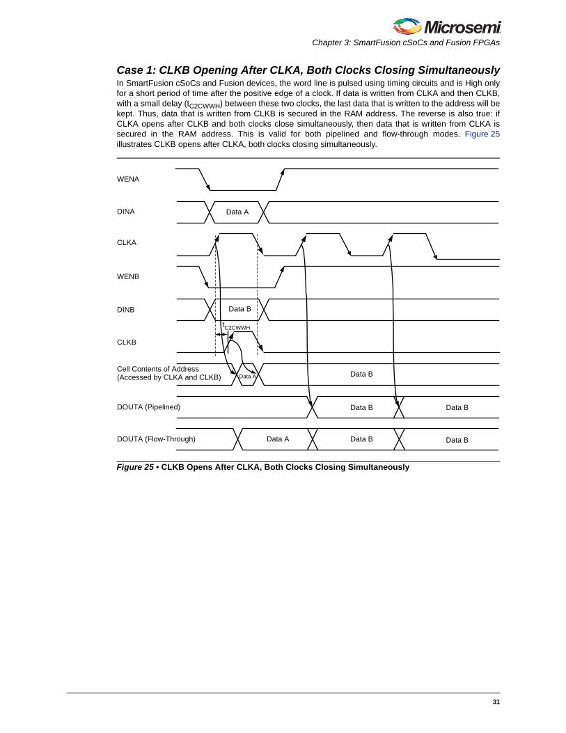
Case 1: CLKB Opening After CLKA, Both Clocks Closing SimultaneouslyIn SmartFusion cSoCs and Fusion devices, the word line is pulsed using timing circuits and is High onlyfor a short period of time after the positive edge of a clock. If data is written from CLKA and then CLKB,with a small delay (tC2CWWH) between these two clocks, the last data that is written to the address will bekept. Thus, data that is written from CLKB is secured in the RAM address. The reverse is also true: ifCLKA opens after CLKB and both clocks close simultaneously, then data that is written from CLKA issecured in the RAM address. This is valid for both pipelined and flow-through modes. Figure 25illustrates CLKB opens after CLKA, both clocks closing simultaneously.
Figure 25 • CLKB Opens After CLKA, Both Clocks Closing Simultaneously
Data A
WENA
DINA
CLKA
WENB
Data BDINB
CLKB
Data A Data B
Data A
Cell Contents of Address (Accessed by CLKA and CLKB)
DOUTA (Pipelined)
DOUTA (Flow-Through)
Data B
Data B
Data B
Data B
tC2CWWH
31
Simultaneous Read-Write Operations in Dual-Port SRAM for Flash-Based cSoCs and FPGAs
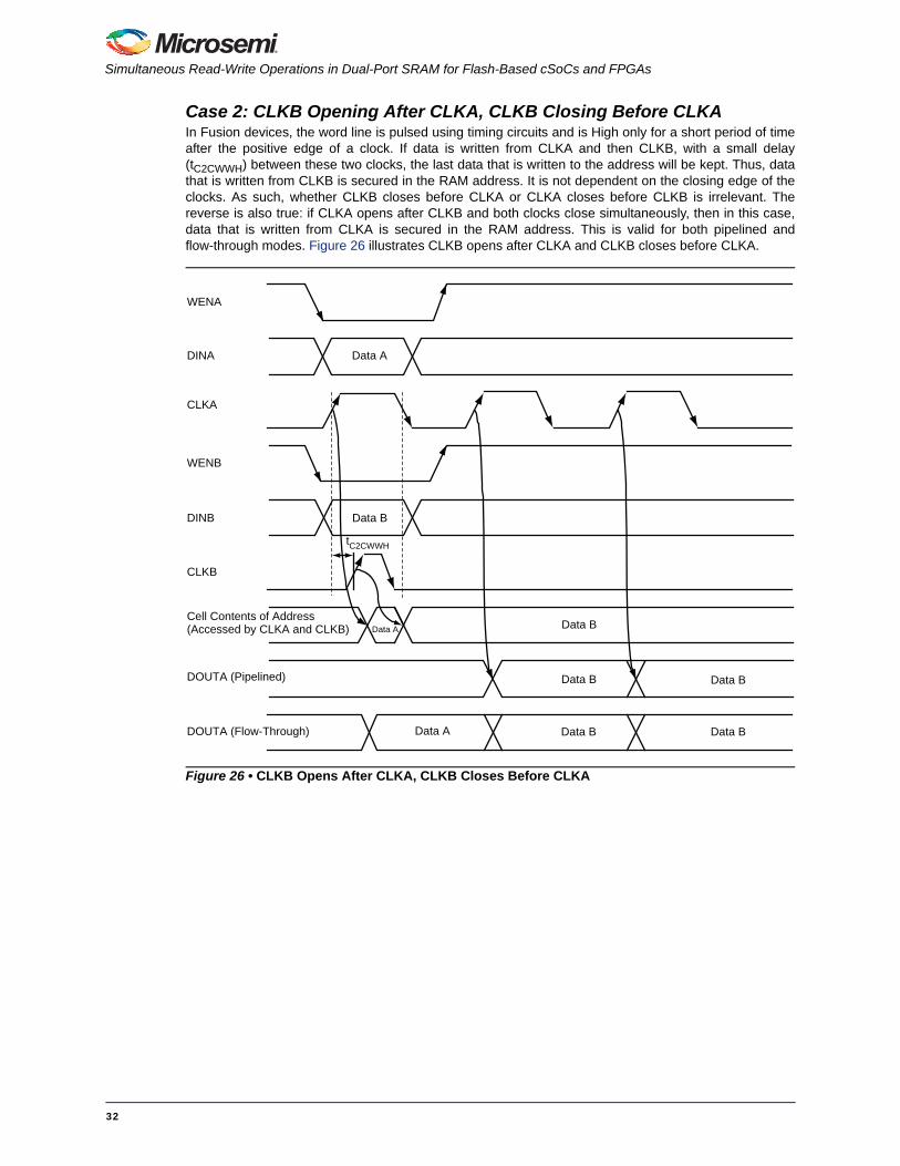
Case 2: CLKB Opening After CLKA, CLKB Closing Before CLKAIn Fusion devices, the word line is pulsed using timing circuits and is High only for a short period of timeafter the positive edge of a clock. If data is written from CLKA and then CLKB, with a small delay(tC2CWWH) between these two clocks, the last data that is written to the address will be kept. Thus, datathat is written from CLKB is secured in the RAM address. It is not dependent on the closing edge of theclocks. As such, whether CLKB closes before CLKA or CLKA closes before CLKB is irrelevant. Thereverse is also true: if CLKA opens after CLKB and both clocks close simultaneously, then in this case,data that is written from CLKA is secured in the RAM address. This is valid for both pipelined andflow-through modes. Figure 26 illustrates CLKB opens after CLKA and CLKB closes before CLKA.
Figure 26 • CLKB Opens After CLKA, CLKB Closes Before CLKA
Data A
WENA
DINA
CLKA
WENB
Data BDINB
CLKB
Data A Data B
Data A
Cell Contents of Address (Accessed by CLKA and CLKB)
DOUTA (Pipelined)
DOUTA (Flow-Through)
Data B
Data B
Data B
Data B
tC2CWWH
32

Chapter 3: SmartFusion cSoCs and Fusion FPGAs
Case 3: CLKB Opening After CLKA, CLKA Closing Before CLKBSimilar to case 2, the word line is pulsed using timing circuits and is High only for a short period of timeafter the positive edge of a clock. If data is written from CLKA and then CLKB, with a small delay(tC2CWWH) between these two clocks, the last data that is written to the address will be kept. Thus, datathat is written from CLKB is secured in the RAM address. It is not dependent on the closing edge of theclocks. As such, whether CLKB closes before CLKA or CLKA closes before CLKB is irrelevant. Thereverse is also true: if CLKA opens after CLKB and both clocks close simultaneously, then data that iswritten from CLKA is secured in the RAM address. This is valid for both pipelined and flow-throughmodes. Figure 27 illustrates CLKB opens after CLKA and CLKB closes after CLKA.
Figure 27 • CLKB Opens After CLKA, CLKB Closes After CLKA
Data ADINA
CLKA
Data BDINB
CLKB
Data B
WENB
Data A
WENA
Data ACell Contents of Address (Accessed by CLKA and CLKB)
DOUTA (Pipelined)
DOUTA (Flow-Through)
Data B
Data B
Data B
Data B
Data B
tC2CWWH
33
Simultaneous Read-Write Operations in Dual-Port SRAM for Flash-Based cSoCs and FPGAs
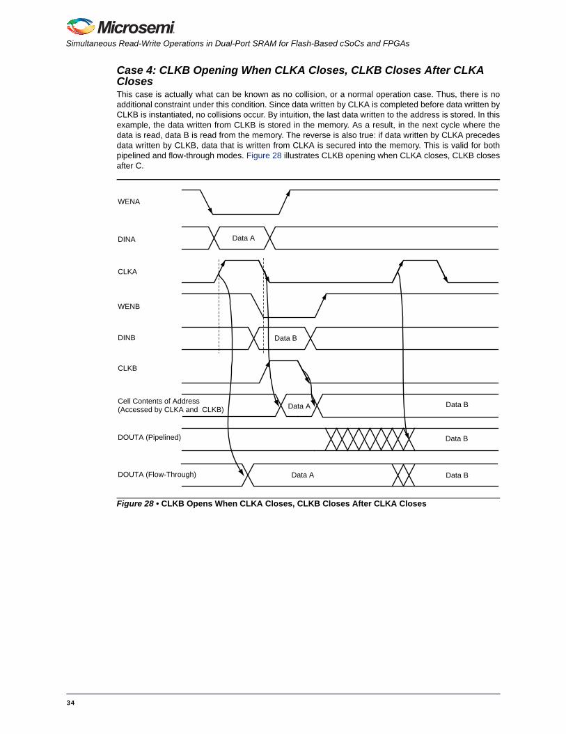
Case 4: CLKB Opening When CLKA Closes, CLKB Closes After CLKA ClosesThis case is actually what can be known as no collision, or a normal operation case. Thus, there is noadditional constraint under this condition. Since data written by CLKA is completed before data written byCLKB is instantiated, no collisions occur. By intuition, the last data written to the address is stored. In thisexample, the data written from CLKB is stored in the memory. As a result, in the next cycle where thedata is read, data B is read from the memory. The reverse is also true: if data written by CLKA precedesdata written by CLKB, data that is written from CLKA is secured into the memory. This is valid for bothpipelined and flow-through modes. Figure 28 illustrates CLKB opening when CLKA closes, CLKB closesafter C.
Figure 28 • CLKB Opens When CLKA Closes, CLKB Closes After CLKA Closes
CLKA
CLKB
WENB
WENA
Cell Contents of Address (Accessed by CLKA and CLKB)
DOUTA (Pipelined)
DOUTA (Flow-Through)
DINA
DINB
Data A
Data B
Data B
Data B
Data B
Data A
Data A
34

Chapter 3: SmartFusion cSoCs and Fusion FPGAs
Case 5: CLKB Opening After CLKA Closes, CLKB Closes After CLKA ClosesSimilar to case 4, there is no collision in this scenario; it is considered a normal operation case. Sincedata written by CLKA is completed before data written by CLKB is instantiated, no collisions occur. Byintuition, the last data written to the address is stored. In this example, the data written from CLKB isstored in the memory. As a result, in the next cycle where the data is read, data B is read from thememory. The reverse is also true: if data written by CLKA precedes data written by CLKB, data that iswritten from CLKA is secured into the memory. This is valid for both pipelined and flow-through modes.Figure 29 illustrates CLKB opening after CLKA closes and CLKB closing after CLKA closes.
Figure 29 • CLKB Opens After CLKA Closes, CLKB Closes After CLKA Closes
Data A
CLKA
CLKB
WENB
WENA
Cell Contents of Address (Accessed by CLKA and CLKB)
DOUTA (Pipelined)
DOUTA (Flow-Through)
Data B
DINA
DINB
Data A
Data A Data B
Data B
Data B
35
Simultaneous Read-Write Operations in Dual-Port SRAM for Flash-Based cSoCs and FPGAs
Simultaneous Read-Write and Write-Read OperationsSimultaneous read-write is defined as the situation when the two clocks, CLKA and CLKB, turn on veryclose to one another to initiate one write operation and one read operation on the same address of theRAM. The behavior in a read-write or a write-read situation depends on what occurs at the positive or theopening edge of the clock. The word line is pulsed using timing circuits and is High only for a short periodof time after the positive edge of a clock. Therefore, only a small delay is required between the positiveedges of CLKA and CLKB in order to successfully perform a simultaneous write-read or read-writeoperations. All events except for events having both edges opening simultaneously will have a stable,known output. The various behaviors are described in Table 9. Each case is discussed in detail in thefollowing sections. A write operation is performed for CLKA while a read operation is performed onCLKB.
Table 9 • List of Simultaneous Write-Read, Read-Write Scenarios
Case Description Output When Data is Read
1 Simultaneous clock on falling edge, CLKB risesafter CLKA
Data from CLKA is read
2 CLKB rises after CLKA, CLKB falls before CLKA Data from CLKA is read
3 CLKB rises after CLKA, CLKB falls after CLKA Data from CLKA is read
4 CLKB rises before CLKA, CLKB falls before CLKA Old data from address is read if delaybetween CLKA and CLKB is met;otherwise it would be unknown.
5 Simultaneous clock on falling edge, CLKB risesbefore CLKA
Old data from address is read if delaybetween CLKA and CLKB is met;otherwise it would be unknown.
6 CLKB rises when CLKA falls, CLKB falls after CLKA Data from CLKA is read
7 CLKB rises after CLKA falls, CLKB falls after CLKA Data from CLKA is read
36
Chapter 3: SmartFusion cSoCs and Fusion FPGAs
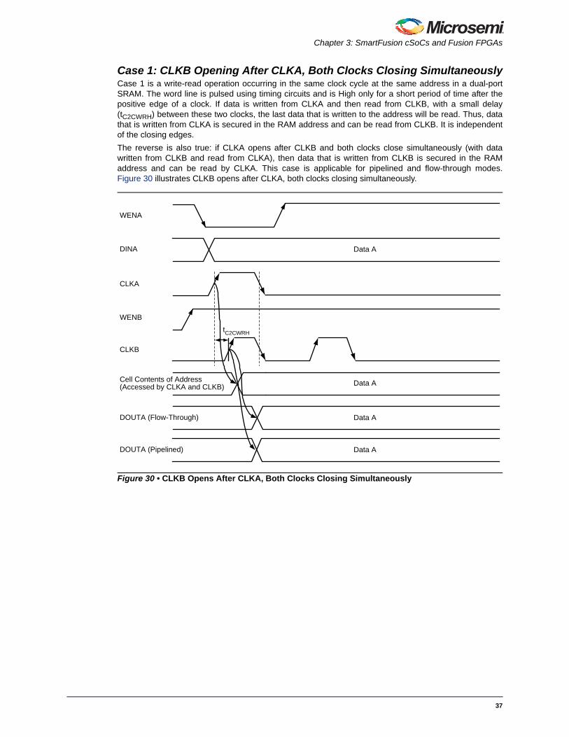
Case 1: CLKB Opening After CLKA, Both Clocks Closing SimultaneouslyCase 1 is a write-read operation occurring in the same clock cycle at the same address in a dual-portSRAM. The word line is pulsed using timing circuits and is High only for a short period of time after thepositive edge of a clock. If data is written from CLKA and then read from CLKB, with a small delay(tC2CWRH) between these two clocks, the last data that is written to the address will be read. Thus, datathat is written from CLKA is secured in the RAM address and can be read from CLKB. It is independentof the closing edges. The reverse is also true: if CLKA opens after CLKB and both clocks close simultaneously (with datawritten from CLKB and read from CLKA), then data that is written from CLKB is secured in the RAMaddress and can be read by CLKA. This case is applicable for pipelined and flow-through modes.Figure 30 illustrates CLKB opens after CLKA, both clocks closing simultaneously.
Figure 30 • CLKB Opens After CLKA, Both Clocks Closing Simultaneously
Data ADINA
CLKA
CLKB
Data A
Data A
Data A
WENB
WENA
Cell Contents of Address (Accessed by CLKA and CLKB)
DOUTA (Pipelined)
DOUTA (Flow-Through)
tC2CWRH
37

Simultaneous Read-Write Operations in Dual-Port SRAM for Flash-Based cSoCs and FPGAs
Case 2: CLKB Opening After CLKA, CLKB Closes Before CLKASimilar to case 1, case 2 is a write-read operation occurring in the same clock cycle at the same addressin a dual-port SRAM. The word line is pulsed using timing circuits and is High only for a short period oftime after the positive edge of a clock. If data is written from CLKA and then read from CLKB, with a smalldelay (tC2CWRH) between these two clocks, the last data that is written to the address will be read. Thus,data that is written from CLKA is secured in the RAM address and can be read from CLKB. The ability ofthe data to be read accurately is independent of the closing edges, regardless of whether the clockedges close simultaneously or asynchronously.The reverse is also true: if CLKA opens after CLKB and CLKA closes before CLKB (with data writtenfrom CLKB and read from CLKA), then data that is written from CLKB is secured in the RAM address andcan be read by CLKA. This case is applicable for pipelined and flow-through modes. Figure 31 illustratesCLKB opens after CLKA and CLKB closes before CLKA.
Figure 31 • CLKB Opens After CLKA, CLKB Closes Before CLKA
DINA Data A
CLKA
CLKB
WENB
WENA
Cell Contents of Address (Accessed by CLKA and CLKB)
DOUTA (Flow-Through)
DOUTA (Pipelined)
Data A
Data A
Data A
tC2CWRH
38

Chapter 3: SmartFusion cSoCs and Fusion FPGAs
Case 3: CLKB Opening After CLKA, CLKB Closes After CLKASimilar to case 1, case 3 is a write-read operation occurring in the same clock cycle at the same addressin a dual-port SRAM. The word line is pulsed using timing circuits and is High only for a short period oftime after the positive edge of a clock, if data is written from CLKA and then read from CLKB, with a smalldelay (tC2CWRH) between these two clocks, the last data that is written to the address will be read. Thus,data that is written from CLKA is secured in the RAM address and can be read from CLKB. The ability ofthe data to be read accurately is independent of the closing edges, regardless of whether the clockedges close simultaneously or asynchronously.The reverse is also true: if CLKA opens after CLKB and CLKA closes before CLKB (with data writtenfrom CLKB and read from CLKA), then in this case, data that is written from CLKB is secured in the RAMaddress and can be read by CLKA. This case is applicable for pipelined and flow-through modes.Figure 32 illustrates CLKB opens after CLKA and CLKB closes after CLKA.
Figure 32 • CLKB Opens After CLKA, CLKB Closes After CLKA
Data ADINA
CLKA
CLKB
WENB
WENA
Cell Contents of Address (Accessed by CLKA and CLKB)
DOUTA (Flow-Through)
DOUTA (Pipelined)
Data A
Data A
Data A
tC2CWRH
39
Simultaneous Read-Write Operations in Dual-Port SRAM for Flash-Based cSoCs and FPGAs
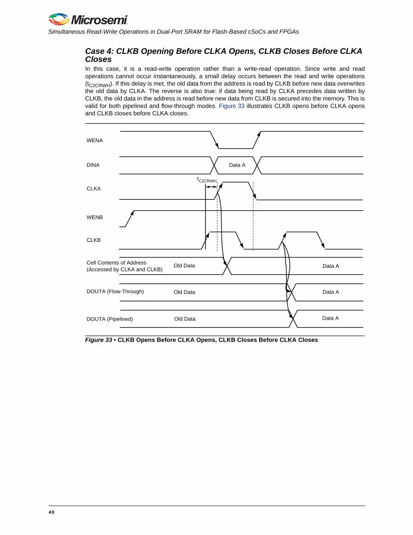
Case 4: CLKB Opening Before CLKA Opens, CLKB Closes Before CLKA ClosesIn this case, it is a read-write operation rather than a write-read operation. Since write and readoperations cannot occur instantaneously, a small delay occurs between the read and write operations(tC2CRWH). If this delay is met, the old data from the address is read by CLKB before new data overwritesthe old data by CLKA. The reverse is also true: if data being read by CLKA precedes data written byCLKB, the old data in the address is read before new data from CLKB is secured into the memory. This isvalid for both pipelined and flow-through modes. Figure 33 illustrates CLKB opens before CLKA opensand CLKB closes before CLKA closes.
Figure 33 • CLKB Opens Before CLKA Opens, CLKB Closes Before CLKA Closes
Data ADINA
CLKA
CLKB
Old Data Data A
WENA
WENB
Cell Contents of Address (Accessed by CLKA and CLKB)
DOUTA (Flow-Through)
DOUTA (Pipelined)
Old Data
Old Data
Data A
Data A
tC2CRWH
40
Chapter 3: SmartFusion cSoCs and Fusion FPGAs
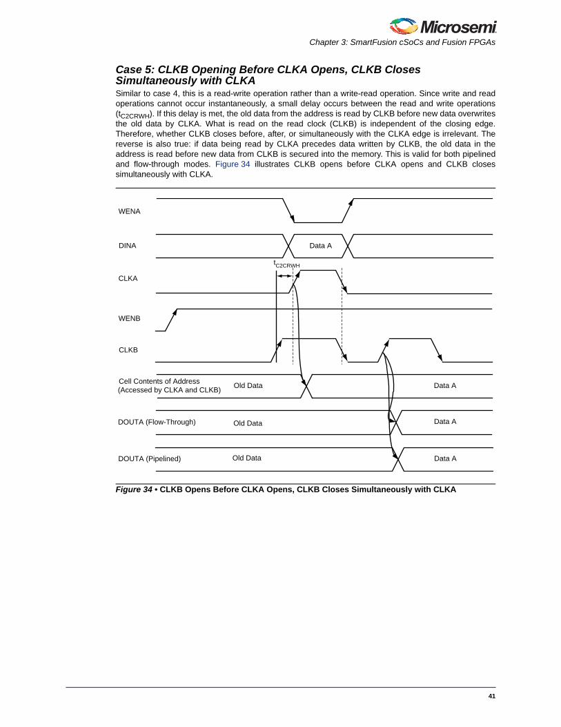
Case 5: CLKB Opening Before CLKA Opens, CLKB Closes Simultaneously with CLKASimilar to case 4, this is a read-write operation rather than a write-read operation. Since write and readoperations cannot occur instantaneously, a small delay occurs between the read and write operations(tC2CRWH). If this delay is met, the old data from the address is read by CLKB before new data overwritesthe old data by CLKA. What is read on the read clock (CLKB) is independent of the closing edge.Therefore, whether CLKB closes before, after, or simultaneously with the CLKA edge is irrelevant. Thereverse is also true: if data being read by CLKA precedes data written by CLKB, the old data in theaddress is read before new data from CLKB is secured into the memory. This is valid for both pipelinedand flow-through modes. Figure 34 illustrates CLKB opens before CLKA opens and CLKB closessimultaneously with CLKA.
Figure 34 • CLKB Opens Before CLKA Opens, CLKB Closes Simultaneously with CLKA
Data ADINA
CLKA
CLKB
Old Data Data A
WENA
WENB
Cell Contents of Address (Accessed by CLKA and CLKB)
DOUTA (Flow-Through)
DOUTA (Pipelined)
Old Data
Old Data
Data A
Data A
tC2CRWH
41
Simultaneous Read-Write Operations in Dual-Port SRAM for Flash-Based cSoCs and FPGAs
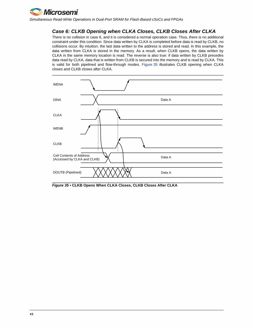
Case 6: CLKB Opening when CLKA Closes, CLKB Closes After CLKAThere is no collision in case 6, and it is considered a normal operation case. Thus, there is no additionalconstraint under this condition. Since data written by CLKA is completed before data is read by CLKB, nocollisions occur. By intuition, the last data written to the address is stored and read. In this example, thedata written from CLKA is stored in the memory. As a result, when CLKB opens, the data written byCLKA in the same memory location is read. The reverse is also true: if data written by CLKB precedesdata read by CLKA, data that is written from CLKB is secured into the memory and is read by CLKA. Thisis valid for both pipelined and flow-through modes. Figure 35 illustrates CLKB opening when CLKAcloses and CLKB closes after CLKA.
Figure 35 • CLKB Opens When CLKA Closes, CLKB Closes After CLKA
DINA
CLKA
CLKB
WENA
WENB
Cell Contents of Address (Accessed by CLKA and CLKB)
DOUTB (Pipelined)
Data A
Data A
Data A
42

Conclusion
Case 7: CLKB Opening After CLKA Closes, CLKB Closes After CLKASimilar to case 6, this is normal operation and there is no collision. Thus, there is no additional constraintunder this condition. Since data written by CLKA is completed before data is read by CLKB, no collisionsoccur. By intuition, the last data written to the address is stored and read. In this example, the datawritten from CLKA is stored in the memory. As a result, when CLKB opens, the data written by CLKA inthe same memory location is read. The reverse is also true: if data written by CLKB precedes data readby CLKA, data that is written from CLKB is secured into the memory and is read by CLKA. This is validfor both pipelined and flow-through modes. Figure 36 illustrates CLKB opening after CLKA closes andCLKB closes after CLKA.
Note: The above descriptions of the cases assume that there are no violations in setup/hold times of thedescribed signals (address setup/hold time and data setup/hold time). Three additional clock-to-clock constraints on the positive or opening edge are required:tC2CWWH – Clock-to-clock constraint for a write-then-write operationtC2CRWH – Clock-to-clock constraint for a read-then-write operationtC2CWRH – Clock-to-clock constraint for a write-then-read operationValues of these timing parameters are available in the datasheets. Refer to the appropriatedatasheets for timing information (Table 7 on page 30).
ConclusionMicrosemi suggests that where at all possible, avoid simultaneous read-write activities to ensure correctdata written and read from the same address. If it is necessary to implement such configurations, beadvised that only the aforementioned cases will provide known output when data is written or read fromthe same address. Review carefully, prior to implementation, whether or not your design satisfies thecriteria discussed here.
Figure 36 • CLKB Opens After CLKA Closes, CLKB Closes After CLKA
DINA
CLKA
CLKB
WENA
WENB
Cell Contents of Address (Accessed by CLKA and CLKB)
DOUTB (Pipelined)
Data A
Data A
Data A
43

51900242-0/8.11
© 2011 Microsemi Corporation. All rights reserved. Microsemi and the Microsemi logo are trademarks of MicrosemiCorporation. All other trademarks and service marks are the property of their respective owners.
Microsemi Corporation (NASDAQ: MSCC) offers a comprehensive portfolio of semiconductorsolutions for: aerospace, defense and security; enterprise and communications; and industrialand alternative energy markets. Products include high-performance, high-reliability analog andRF devices, mixed signal and RF integrated circuits, customizable SoCs, FPGAs, andcomplete subsystems. Microsemi is headquartered in Aliso Viejo, Calif. Learn more atwww.microsemi.com.
Microsemi Corporate HeadquartersOne Enterprise Drive, Aliso Viejo CA 92656Within the USA: (800) 713-4113 Outside the USA: (949) 221-7100 Fax: (949) 756-0308 · www.microsemi.com