single-chip li-ion charge and system power-path … · bq24070, bq24071 slus694g –march...
TRANSCRIPT

IN
BAT
OUT
bq24070/1
PACK+
PACK−
System
VDC
GND
AC Adapter
+
Q1
Q2
UDG−04082
40 mΩ
(2)
Product
Folder
Sample &Buy
Technical
Documents
Tools &
Software
Support &Community
bq24070, bq24071SLUS694G –MARCH 2006–REVISED DECEMBER 2014
bq2407x Single-Chip Li-Ion Charge and System Power-Path Management IC1 Features 3 Description
The bq24070 and bq24071 are highly integrated Li-1• Small 3.5-mm × 4.5-mm VQFN Package
ion linear charger and system power-path• Designed for Single-Cell Li-Ion- or Li-Polymer- management devices targeted at space-limitedBased Portable Applications portable applications. The bq2407x devices offer DC
• Integrated Dynamic Power-Path Management supply (AC adapter) power-path management withautonomous power-source selection, power FETs(DPPM) Feature Allowing the AC Adapter toand current sensors, high-accuracy current andSimultaneously Power the System and Charge thevoltage regulation, charge status, and chargeBatterytermination, in a single monolithic device.• Power Supplement Mode Allows Battery toThe bq2407x devices power the system whileSupplement the AC Input Currentindependently charging the battery. This feature• Autonomous Power Source Selection (AC Adapterreduces the charge and discharge cycles on theor BAT) battery, allows for proper charge termination, and
• Supports Up to 2 A Total Current allows the system to run with an absent or defectivebattery pack. This feature also allows for the system• Thermal Regulation for Charge Controlto instantaneously turn on from an external power• Charge Status Outputs for LED or Systemsource in the case of a deeply discharged batteryInterface Indicates Charge and Fault Conditions pack. The IC design is focused on supplying
• Reverse Current, Short-Circuit, and Thermal continuous power to the system when available fromProtection the AC adapter or battery sources.
• Power Good Status OutputsDevice Information(1)
• 4.4-V and 6-V Options for System OutputPART NUMBER PACKAGE BODY SIZE (NOM)Regulation Voltage
bq24070VQFN (20) 3.50 mm × 4.50 mm
bq240712 Applications(1) For all available packages, see the orderable addendum at• Smart Phones and PDAs
the end of the datasheet.• MP3 Players• Digital Cameras and Handheld Devices• Internet Appliances
Simplified Schematic(1)
(1) See Figure 2 and Functional Block Diagram for more detailed feature information.(2) P-FET back gate body diodes are disconnected to prevent body diode conduction.
1
An IMPORTANT NOTICE at the end of this data sheet addresses availability, warranty, changes, use in safety-critical applications,intellectual property matters and other important disclaimers. PRODUCTION DATA.

bq24070, bq24071SLUS694G –MARCH 2006–REVISED DECEMBER 2014 www.ti.com
Table of Contents8.4 Device Functional Modes........................................ 141 Features .................................................................. 1
9 Application and Implementation ........................ 202 Applications ........................................................... 19.1 Application Information............................................ 203 Description ............................................................. 19.2 Typical Application .................................................. 204 Revision History..................................................... 2
10 Power Supply Recommendations ..................... 235 Device Comparison Table ..................................... 311 Layout................................................................... 236 Pin Configuration and Functions ......................... 3
11.1 Layout Guidelines ................................................. 237 Specifications......................................................... 411.2 Layout Example .................................................... 237.1 Absolute Maximum Ratings ..................................... 411.3 Thermal Considerations ........................................ 247.2 ESD Ratings.............................................................. 4
12 Device and Documentation Support ................. 257.3 Recommended Operating Conditions....................... 412.1 Documentation Support ........................................ 257.4 Thermal Information .................................................. 512.2 Related Links ........................................................ 257.5 Electrical Characteristics........................................... 512.3 Trademarks ........................................................... 257.6 Typical Characteristics .............................................. 812.4 Electrostatic Discharge Caution............................ 258 Detailed Description .............................................. 912.5 Glossary ................................................................ 258.1 Overview ................................................................... 9
13 Mechanical, Packaging, and Orderable8.2 Functional Block Diagram ....................................... 10Information ........................................................... 258.3 Feature Description................................................. 11
4 Revision History
Changes from Revision F (December 2009) to Revision G Page
• Added ESD Ratings table, Feature Description section, Device Functional Modes, Application and Implementationsection, Power Supply Recommendations section, Layout section, Device and Documentation Support section, andMechanical, Packaging, and Orderable Information section .................................................................................................. 1
2 Submit Documentation Feedback Copyright © 2006–2014, Texas Instruments Incorporated
Product Folder Links: bq24070 bq24071

STAT2
IN
BAT
BAT
ISET2
MODE
CE
PG
OUT
OUT
OUT
TMR
DPPM
TS
GN
D
VR
EF
VS
S
ISE
T1
201
1110
2
3
4
5
6
7
8
9
19
18
17
16
15
14
13
12
STAT1 GND
bq24070, bq24071www.ti.com SLUS694G –MARCH 2006–REVISED DECEMBER 2014
5 Device Comparison Table
PART BATTERY PACKAGETA OUT PIN STATUSNUMBER (1) VOLTAGE (V) MARKINGbq24070 Regulated to 4.4 V (2) BRQ
–40°C to 125°C 4.2 Productionbq24071 Regulated to 6 V BTR
(1) This product is RoHS compatible, including a lead concentration that does not exceed 0.1% of total product weight, and is suitable foruse in specified lead-free soldering processes. In addition, this product uses package materials that do not contain halogens, includingbromine (Br) or antimony (Sb) above 0.1% of total product weight.
(2) If IN < VO(OUT-REG), the IN is connected to the OUT pin by a P-FET, (Q1).
6 Pin Configuration and Functions
RHL Package20 Pins
Top View
Pin FunctionsPIN
I/O DESCRIPTIONNAME NO.BAT 5, 6 I/O Battery input and output.CE 9 I Chip enable input (active high)DPPM 13 I Dynamic power-path management set point (account for scale factor)GND 19, 20 I Ground inputIN 4 I Charge input voltageISET1 10 I/O Charge current set point and precharge and termination set point
Charge current set point for USB port. (High = 500 mA, Low = 100 mA) See half-charge current modeISET2 7 I using ISET2.MODE 8 I Power source selection input (Low for USB mode current limit)OUT 15, 16, 17 O Output terminal to the systemPG 18 O Power-good status output (open-drain)STAT1 2 O Charge status output 1 (open-drain)STAT2 3 O Charge status output 2 (open-drain)
Timer program input programmed by resistor. Disable fast-charge safety timer and termination by tyingTMR 14 I/O TMR to VREF.TS 12 I/O Temperature sense input
Copyright © 2006–2014, Texas Instruments Incorporated Submit Documentation Feedback 3
Product Folder Links: bq24070 bq24071
bq24070, bq24071SLUS694G –MARCH 2006–REVISED DECEMBER 2014 www.ti.com
Pin Functions (continued)PIN
I/O DESCRIPTIONNAME NO.VREF 1 O Internal reference signal
Ground input (the thermal pad on the underside of the package) There is an internal electrical connectionbetween the exposed thermal pad and VSS pin of the device. The exposed thermal pad must beVSS 11 – connected to the same potential as the VSS pin on the printed-circuit board. Do not use the thermal pad asthe primary ground input for the device. VSS pin must be connected to ground at all times.
7 Specifications
7.1 Absolute Maximum Ratings (1)
over operating free-air temperature range (unless otherwise noted)MIN MAX UNIT
Input voltage IN (DC voltage with respect to VSS) –0.3 18BAT, CE, DPPM, PG, Mode, OUT, ISET1, ISET2, STAT1, STAT2, TS, (all DC –0.3 7voltages with respect to VSS)
VInput voltage VO(OUT) +VREF (DC voltage with respect to VSS) –0.3 0.3
TMR –0.3 VO + 0.3Input current 3.5
OUT 4 AOutput current
BAT (2) –4 3.5Output sourcecurrent (in VREF 30 mAregulation at3.3-V VREF)Output sink PG, STAT1, STAT2, 15 mAcurrentJunction temperature, TJ –40 150Lead temperature (soldering, 10 s) 300 °CStorage temperature, Tstg –65 150
(1) Stresses beyond those listed under Absolute Maximum Ratings may cause permanent damage to the device. These are stress ratingsonly, and functional operation of the device at these or any other conditions beyond those indicated under Recommended OperatingConditions is not implied. Exposure to absolute-maximum-rated conditions for extended periods may affect device reliability. All voltagevalues are with respect to the network ground terminal unless otherwise noted.
(2) Negative current is defined as current flowing into the BAT pin.
7.2 ESD RatingsVALUE UNIT
Human body model (HBM), per ANSI/ESDA/JEDEC JS-001 (1) ±1000V(ESD) Electrostatic discharge VCharged-device model (CDM), per JEDEC specification JESD22- ±250
C101 (2)
(1) JEDEC document JEP155 states that 500-V HBM allows safe manufacturing with a standard ESD control process. Manufacturing withless than 500-V HBM is possible with the necessary precautions. Pins listed as ±XXX V may actually have higher performance.
(2) JEDEC document JEP157 states that 250-V CDM allows safe manufacturing with a standard ESD control process. Manufacturing withless than 250-V CDM is possible with the necessary precautions. Pins listed as ±YYY V may actually have higher performance.
7.3 Recommended Operating ConditionsMIN MAX UNIT
VCC Supply voltage (VIN) (1) 4.35 16 VIIN Input current 2 ATJ Operating junction temperature range –40 125 °C
(1) Verify that power dissipation and junction temperatures are within limits at maximum VCC .
4 Submit Documentation Feedback Copyright © 2006–2014, Texas Instruments Incorporated
Product Folder Links: bq24070 bq24071

bq24070, bq24071www.ti.com SLUS694G –MARCH 2006–REVISED DECEMBER 2014
7.4 Thermal Informationbq2407x
THERMAL METRIC (1) RHL UNIT20 PINS
RθJA Junction-to-ambient thermal resistance 40.1RθJC(top) Junction-to-case (top) thermal resistance 42.0RθJB Junction-to-board thermal resistance 16.6
°C/WψJT Junction-to-top characterization parameter 0.7ψJB Junction-to-board characterization parameter 16.6RθJC(bot) Junction-to-case (bottom) thermal resistance 4.2
(1) For more information about traditional and new thermal metrics, see the IC Package Thermal Metrics application report, SPRA953.
7.5 Electrical Characteristicsover junction temperature range (0°C ≤ TJ ≤ 125°C) and the recommended supply voltage range (unless otherwise noted)
PARAMETER TEST CONDITIONS MIN TYP MAX UNIT
INPUT BIAS CURRENTS
ICC(SPLY) Active supply current, VCC VVCC > VVCC(min) 1 2 mA
VIN < V(BAT)Sleep current (current into BATICC(SLP) 2.6 V ≤ VI(BAT) ≤ VO(BAT-REG), 2 5pin) Excludes load on OUT pin
VI(IN) ≤ 6V, Total current into IN pin with chipICC(IN-STDBY) Input standby current disabled, Excludes all loads, CE=LOW, after 200
t(CE-HOLDOFF) delayμA
Total current into BAT pin with input presentand chip disabled;
ICC(BAT-STDBY) BAT standby current Excludes all loads, CE=LOW, 45 65after t(CE-HOLDOFF) delay,0°C ≤ TJ ≤ 85°C (1)
IIB(BAT) Charge done current, BAT Charge DONE, input supplying the load 1 5
OUT PIN-VOLTAGE REGULATION
bq24070 VI(IN) ≥ 4.4 V + VDO 4.4 4.5Output regulationVO(OUT-REG) Vvoltage bq24071 VI(IN) ≥ 6 V + VDO 6.0 6.3
OUT PIN – DPPM REGULATION
V(DPPM-SET) DPPM set point (2) VDPPM-SET < VOUT 2.6 3.8 V
I(DPPM-SET) DPPM current source Input present 95 100 105 μA
SF DPPM scale factor V(DPPM-REG) = V(DPPM-SET) × SF 1.139 1.150 1.162
OUT PIN – FET (Q1, Q2) DROP-OUT VOLTAGE RDS(on))
VI(IN) ≥ VCC(min), Mode = High,V(INDO) IN-to-OUT dropout voltage (3) 300 475II(IN) = 1 A, (IO(OUT)+ IO(BAT)), or no inputmV
BAT-to-OUT dropout voltageV(BATDO) VI (BAT) ≥ 3 V, II(BAT)= 1.0 A, VCC < VI(BAT) 40 100(discharging)
(1) This includes the quiescent current for the integrated LDO.(2) V(DPPM-SET) is scaled up by the scale factor for controlling the output voltage V(DPPM-REG).(3) VDO(max), dropout voltage is a function of the FET, RDS(on), and drain current. The dropout voltage increases proportionally to the
increase in current.
Copyright © 2006–2014, Texas Instruments Incorporated Submit Documentation Feedback 5
Product Folder Links: bq24070 bq24071
bq24070, bq24071SLUS694G –MARCH 2006–REVISED DECEMBER 2014 www.ti.com
Electrical Characteristics (continued)over junction temperature range (0°C ≤ TJ ≤ 125°C) and the recommended supply voltage range (unless otherwise noted)
PARAMETER TEST CONDITIONS MIN TYP MAX UNIT
OUT PIN - BATTERY SUPPLEMENT MODE
Enter battery supplement mode VI(OUT)VBSUP1 (battery supplements OUT current VI(BAT)> 2 V ≤ VI(BAT)
in the presence of input source – 60 mVV
VI(OUT)VBSUP2 Exit battery supplement mode VI(BAT)> 2 V ≥ VI(BAT)
– 20 mV
OUT PIN - SHORT CIRCUIT
Current source between BAT to OUT forIOSH1 BAT to OUT short-circuit recovery short-circuit recovery to 10 mA
VI(OUT) ≤ VI(BAT) –200 mV
RSHIN IN to OUT short-circuit limit VI(OUT) ≤ 1 V 500 Ω
BAT PIN CHARGING – PRECHARGE
Precharge to fast-charge transitionV(LOWV) Voltage on BAT 2.9 3 3.1 Vthreshold
Deglitch time for fast-charge to tFALL = 100 ns, 10 mV overdrive,TDGL(F) 22.5 msprecharge transition (4) VI(BAT) decreasing below threshold
1 V < VI(BAT) < V(LOWV), t < t(PRECHG),IO(PRECHG) Precharge range 10 150 mAIO(PRECHG) = (K(SET) × V(PRECHG))/ RSET
V(PRECHG) Precharge set voltage 1 V < VI(BAT) < V(LOWV), t < t(PRECHG) 225 250 275 mV
BAT PIN CHARGING - CURRENT REGULATION
VI (BAT) > V(LOWV), Mode = HighIO(BAT) Battery charge current range (5) IOUT(BAT) = (K(SET) × V(SET) / RSET), 100 1000 1500 mA
VI(OUT) > VO(OUT-REG) + V(DO-MAX)
RPBAT BAT to OUT pullup VI (BAT)< 1 V 1000 Ω
Voltage on ISET1, VVCC ≥ 4.35 V,Battery charge current setV(SET) VI(OUT)- VI(BAT) > V(DO-MAX), 2.47 2.50 2.53 Vvoltage (6)VI(BAT) > V(LOWV)
100 mA ≤ IO(BAT) ≤ 1.5 A 375 425 450K(SET) Charge current set factor, BAT
10 mA ≤ IO(BAT) ≤ 100 mA (7) 300 450 600
USB MODE INPUT CURRENT LIMIT
ISET2 = Low 80 90 100I(USB) USB input port current range mA
ISET2 = High 400 500
BAT PIN CHARGING VOLTAGE REGULATION, VO (BAT-REG) + V (DO-MAX) < VCC, ITERM < IBAT(OUT) ≤ 1 A
Battery charge voltage 4.2 V
VO(BAT-REG) TA = 25°C –0.5% 0.5%Battery charge voltage regulationaccuracy –1% 1%
CHARGE TERMINATION DETECTION
Charge termination detection VI(BAT) > V(RCH),I(TERM) 10 150 mArange I(TERM) = (K(SET) × V(TERM))/ RSET
VI(BAT) > V(RCH) , Mode = High 230 250 270Charge termination set voltage,V(TERM) mVmeasured on ISET1 VI(BAT) > V(RCH) , Mode = Low 95 100 130
tFALL = 100 ns, 10 mV overdrive,Deglitch time for terminationTDGL(TERM) ICHG increasing above or decreasing below 22.5 msdetection threshold
TEMPERATURE SENSE COMPARATORS
VLTF High voltage threshold Temp fault at V(TS) > VLTF 2.465 2.500 2.535 V
VHTF Low voltage threshold Temp fault at V(TS) < VHTF 0.485 0.500 0.515 V
ITS Temperature sense current source 94 100 106 μA
R(TMR) = 50 kΩ, VI(BAT) increasing orDeglitch time for temperature faultTDGL(TF) decreasing above and below; 22.5 msdetection (4)100-ns fall time, 10-mv overdrive
(4) All deglitch periods are a function of the timer setting and is modified in DPPM or thermal regulation modes by the percentages that theprogram current is reduced.
(5) When input current remains below 2 A, the battery charging current may be raised until the thermal regulation limits the charge current.(6) For half-charge rate, V(SET) is 1.25 V ± 25 mV.(7) Specification is for monitoring charge current through the ISET1 pin during voltage regulation mode, not for a reduced fast-charge level.
6 Submit Documentation Feedback Copyright © 2006–2014, Texas Instruments Incorporated
Product Folder Links: bq24070 bq24071
bq24070, bq24071www.ti.com SLUS694G –MARCH 2006–REVISED DECEMBER 2014
Electrical Characteristics (continued)over junction temperature range (0°C ≤ TJ ≤ 125°C) and the recommended supply voltage range (unless otherwise noted)
PARAMETER TEST CONDITIONS MIN TYP MAX UNIT
BATTERY RECHARGE THRESHOLD
VO(BAT- VO(BAT-REG) VO(BAT-REG)VRCH Recharge threshold voltage REG) V–0.100 –0.125–0.075
R(TMR) = 50 kΩ, VI(BAT) increasingDeglitch time for rechargeTDGL(RCH) or decreasing below threshold, 22.5 msdetection (4)100-ns fall time, 10-mv overdrive
STAT1, STAT2, AND PG, OPEN-DRAIN (OD) OUTPUTS (8)
IOL = 5 mA, An external pullupVOL Low-level output saturation voltage 0.25 Vresistor ≥ 1 K required.
ILKG Input leakage current 1 5 μA
ISET2, CE INPUTS
VIL Low-level input voltage 0 0.4V
VIH High-level input voltage 1.4
IIL Low-level input current, CE –1
IIH High-level input current, CE 1μA
IIL Low-level input current, ISET2 VISET2 = 0.4 V –20
IIH High-level input current, ISET2 VISET2 = VCC 40
t(CE-HLDOFF) Holdoff time, CE CE going low only 3.3 6.2 ms
MODE INPUT
Falling Hi→Low; 280 K ± 10% applied whenVIL Low-level input voltage 0.975 1 1.025 Vlow.
VIH High-level input voltage Input RMode sets external hysteresis VIL + .01 VIL + .024 V
IIL Low-level input current, Mode –1 μA
TIMERS
K(TMR) Timer set factor t(CHG) = K(TMR) × R(TMR) 0.313 0.360 0.414 s/Ω
R(TMR)(9) External resistor limits 30 100 kΩ
0.09 ×t(PRECHG) Precharge timer 0.10 × t(CHG) 0.11 × t(CHG) st(CHG)
Timer fault recovery pullup fromI(FAULT) 1 kΩOUT to BAT
CHARGER SLEEP THRESHOLDS (PG THRESHOLDS, LOW → POWER GOOD)
VVCC ≤V(UVLO) ≤ VI(BAT) ≤ VO(BAT-REG),V(SLPENT)(10) Sleep-mode entry threshold VI(BAT)No t(BOOT-UP) delay +125 mV
VVVCC ≥V(UVLO) ≤ VI(BAT) ≤ VO(BAT-REG),V(SLPEXIT)
(10) Sleep-mode exit threshold VI(BAT)No t(BOOT-UP) delay +190 mV
R(TMR) = 50 kΩ,t(DEGL) Deglitch time for sleep mode (11) V(IN) decreasing below threshold, 100-ns fall 22.5 ms
time, 10-mv overdrive
START-UP CONTROL BOOT-UP
On the first application of input with Modet(BOOT-UP) Boot-up time 120 150 180 msLow
(8) See Charger Sleep mode for PG (VCC = VIN) specifications.(9) To disable the fast-charge safety timer and charge termination, tie TMR to the VREF pin. Tying the TMR pin high changes the timing
resistor from the external value to an internal 50 kΩ ±25%, which can add an additional tolerance to any timed specification. The TMRpin normally regulates to 2.5 V when the charge current is not restricted by the DPPM or thermal feedback loops. If these loops becomeactive, the TMR pin voltage will be reduced proportionally to the reduction in charge current and the clock frequency will be reduced bythe same percentage (timed durations will count down slower, extending their time). The TMR pin is clamped at 0.80 V, for a maximumtime extension of 2.5 V ÷ 0.8 V × 100 = 310%.
(10) The IC is considered in sleep mode when IN is absent (PG = OPEN DRAIN).(11) Does not declare sleep mode until after the deglitch time and implement the needed power transfer immediately according to the
switching specification.
Copyright © 2006–2014, Texas Instruments Incorporated Submit Documentation Feedback 7
Product Folder Links: bq24070 bq24071
T - Temperatures - Co
Vo
ltag
e -
V
4.36
4.32140
4.38
4.42
4.4
4.44
4.34
-60 -40 -20 0 20 40 60 80 100 120
V , V = 5.5 V
I = 100 AOUT AC
I +3 Sigma
-3 Sigma
Mean
bq24070, bq24071SLUS694G –MARCH 2006–REVISED DECEMBER 2014 www.ti.com
Electrical Characteristics (continued)over junction temperature range (0°C ≤ TJ ≤ 125°C) and the recommended supply voltage range (unless otherwise noted)
PARAMETER TEST CONDITIONS MIN TYP MAX UNIT
SWITCHING POWER SOURCE TIMING
When input applied. Measure from:Switching power source from input [PG: Lo → Hi to I(IN) > 5 mA],tSW-BAT 50 μsto battery I(OUT) = 100 mA,
RTRM = 50 K
THERMAL SHUTDOWN REGULATION (12)
T(SHTDWN) Temperature trip TJ (Q1 and Q3 only) 155
Thermal hysteresis TJ (Q1 and Q3 only) 30 °C
TJ(REG) Temperature regulation limit TJ (Q2) 115 135
UVLO
V(UVLO) Undervoltage lockout Decreasing VCC 2.45 2.50 2.65 V
Hysteresis 27 mV
VREF OUTPUT
Active only if IN or USB is present,VO(VREF) Output regulation voltage 3.3 VVI(OUT) ≥ VO(VREF) + (IO(VREF) × RDS(on))
Regulation accuracy (13) –5% 5%
IO(VREF) Output current 20 mA
RDS(on) On resistance OUT to VREF 50 Ω
C(OUT)(14) Output capacitance 1 μF
(12) Reaching thermal regulation reduces the charging current. Battery supplement current is not restricted by either thermal regulation orshutdown. Input power FETs turn off during thermal shutdown. The battery FET is only protected by a short-circuit limit which typicallydoes not cause a thermal shutdown (input FETs turning off) by itself.
(13) In standby mode (CE low) the accuracy is ±10%.(14) VREF output capacitor not required, but one with a value of 0.1 μF is recommended.
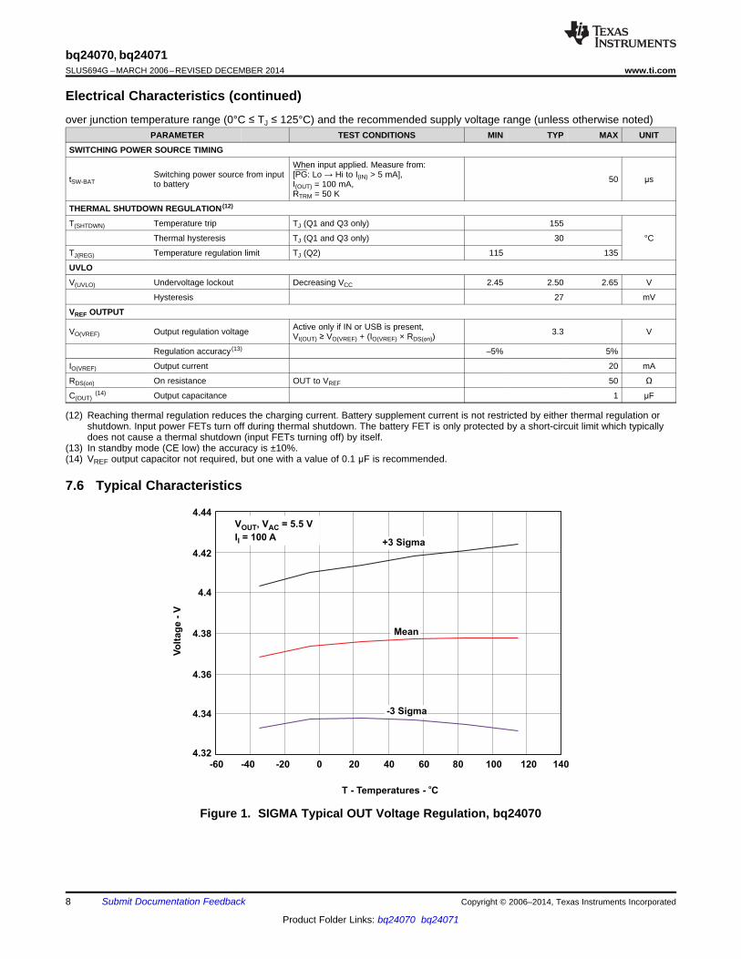
7.6 Typical Characteristics
Figure 1. SIGMA Typical OUT Voltage Regulation, bq24070
8 Submit Documentation Feedback Copyright © 2006–2014, Texas Instruments Incorporated
Product Folder Links: bq24070 bq24071

Pre-ConditioningPhase Current Regulation Phase Voltage Regulation and Charge T ermination Phase
RegulationVoltage
RegulationCurrent
MinimumChargeVoltage
Pre−Conditioning
and TermDetect
ChargeCurrent
ChargeComplete
UDG−04087
ChargeVoltage
bq24070, bq24071www.ti.com SLUS694G –MARCH 2006–REVISED DECEMBER 2014
8 Detailed Description
8.1 OverviewThe bq2407x device is a highly-integrated Li-ion linear charger and system power-path management devicetargeted at space-limited portable applications. The bq2407x devices offer DC supply (AC adapter) power-pathmanagement with autonomous power-source selection, power FETs and current sensors, high-accuracy currentand voltage regulation, charge status, and charge termination, in a single monolithic device.
The bq2407x devices support a precision Li-ion or Li-polymer charging system suitable for single-cell portabledevices. See a typical charge profile, application circuits, and an operational flow chart in Figure 2 throughFigure 6, respectively.
Figure 2. Charge Profile
The bq2407x devices power the system while independently charging the battery. This feature reduces thecharge and discharge cycles on the battery, allows for proper charge termination and allows the system to runwith an absent or defective battery pack. This feature also allows for the system to instantaneously turn on froman external power source in the case of a deeply discharged battery pack. The IC design is focused on supplyingcontinuous power to the system when available from the AC adapter or battery sources.
Copyright © 2006–2014, Texas Instruments Incorporated Submit Documentation Feedback 9
Product Folder Links: bq24070 bq24071

IN
ISET2
Thermal
Shutdown
Precharge
Recharge
Term
STAT1
STAT2
MODE
Suspend
Sleep
VSS
TS
BAT Charge Enable
500 mA/ 100 mA
*
*
*
*
*
*
*Signal Deglitched
UVLO
+
+
1 V
DPPM
Power Source Selection
+
+
++
60 mV
200 mV
+
+
+
+
Disable−
Sleep
DPPM
Scaling
ISET1
BAT
AC Charge Enable
Q2
BATShort−Circuit
Recovery
BAT
Charge
Enable
Short−Circuit Recovery
+
Q1
AC
100 mA /
500 mA
+
GND
Oscillator
500 Ω
VO(OUT)
VI(BAT)
VI(ISET1)
1 kΩ
I(SNS)
VO(OUT)
VO(OUT−REG)
VIO(AC) ChargeEnable
VO(BAT−REG)
VI(BAT)VO(BAT−REG)
VI(BAT)
VI(ISET1)
Fast PrechargeVO(OUT)
I(DPPM)
VSET
VSET
VDPPM
TJ
TJ(REG)V(HTF)
V(LTF)
VO(BAT−REG)
VBAT
VBAT
CE
I(TS)
VI(ISET1)
VBAT
VIN
VI(BAT)
VO(OUT)
V(SET)
C/S − 100 mA
1C − 500 mA
Fast Precharge
PG
GND
ChargeControlTimerand
DisplayLogic
UDG−04084
Recovery
Fault
10 mA
1 V
280 kΩ
VI (SNS)
TMR
OUT
VREF3.3 V
bq24070, bq24071SLUS694G –MARCH 2006–REVISED DECEMBER 2014 www.ti.com
8.2 Functional Block Diagram
10 Submit Documentation Feedback Copyright © 2006–2014, Texas Instruments Incorporated
Product Folder Links: bq24070 bq24071

IN
BAT
OUT
bq24070/1
PACK+
PACK−
System
VDC
GND
AC Adapter
+
Q1
Q2
UDG−04082
40 mΩ
(2)
bq24070, bq24071www.ti.com SLUS694G –MARCH 2006–REVISED DECEMBER 2014
8.3 Feature Description
8.3.1 Power-Path ManagementThe bq2407x devices power the system while independently charging the battery. This feature reduces thecharge and discharge cycles on the battery, allows for proper charge termination, and allows the system to runwith an absent or defective battery pack. This feature gives the system priority on input power, allowing thesystem to power up with a deeply discharged battery pack. This feature works as follows:
Figure 3. Power-Path Management
8.3.1.1 Case 1: IN Mode (Mode = High)
8.3.1.1.1 System Power
In this case, the system load is powered directly from the AC adapter through the internal transistor Q1 (seeFigure 3). The output is regulated at 4.4 V (bq24070). If the system load exceeds the capacity of the supply, theoutput voltage drops down to the voltage of the battery.
8.3.1.1.2 Charge Control
When in IN mode, the battery is charged through switch Q2 based on the charge rate set on the ISET1 input.
8.3.1.1.3 Dynamic Power-Path Management (DPPM)
This feature monitors the output voltage (system voltage) for input power loss due to brown outs, current limiting,or removal of the input supply. If the voltage on the OUT pin drops to a preset value, V(DPPM) × SF, due to alimited amount of input current, then the battery charging current is reduced until the output voltage stopsdropping. The DPPM control tries to reach a steady-state condition where the system gets its needed current andthe battery is charged with the remaining current. No active control limits the current to the system; therefore, ifthe system demands more current than the input can provide, the output voltage drops just below the batteryvoltage and Q2 turns on which supplements the input current to the system. DPPM has three main advantages.1. This feature allows the designer to select a lower power wall adapter, if the average system load is moderate
compared to its peak power. For example, if the peak system load is 1.75 A, average system load is 0.5 Aand battery fast-charge current is 1.25 A, the total peak demand could be 3 A. With DPPM, a 2-A adaptorcould be selected instead of a 3.25-A supply. During the system peak load of 1.75 A and charge load of 1.25A, the smaller adaptor’s voltage drops until the output voltage reaches the DPPM regulation voltagethreshold. The charge current is reduced until there is no further drop on the output voltage. The system getsits 1.75-A charge and the battery charge current is reduced from 1.25 A to 0.25 A. When the peak systemload drops to 0.5 A, the charge current returns to 1 A and the output voltage returns to its normal value.
2. Using DPPM provides a power savings compared to configurations without DPPM. Without DPPM, if thesystem current plus charge current exceed the supply’s current limit, then the output is pulled down to thebattery. Linear chargers dissipate the unused power (VIN-VOUT) × ILOAD. The current remains high (at currentlimit) and the voltage drop is large for maximum power dissipation. With DPPM, the voltage drop is less (VIN-V(DPPM-REG)) to the system which means better efficiency. The efficiency for charging the battery is the samefor both cases. The advantages include less power dissipation, lower system temperature, and better overallefficiency.
3. If possible, the DPPM sustains the system voltage no matter what causes it to drop. The DPPM does this byreducing the noncritical charging load while maintaining the maximum power output of the adaptor.
Copyright © 2006–2014, Texas Instruments Incorporated Submit Documentation Feedback 11
Product Folder Links: bq24070 bq24071

V(DPPM−REG) I(DPPM) R(DPPM) SF= × ×
V(DPPM−REG) I(DPPM) R(DPPM) SF= × ×
bq24070, bq24071SLUS694G –MARCH 2006–REVISED DECEMBER 2014 www.ti.com
Feature Description (continued)The DPPM voltage, V(DPPM), is programmed as follows:
where• R(DPPM) is the external resistor connected between the DPPM and VSS pins• I(DPPM) is the internal current source• SF is the scale factor as specified in the specification table (1)
The safety timer is dynamically adjusted while in DPPM mode. The voltage on the ISET1 pin is directlyproportional to the programmed charging current. When the programmed charging current is reduced, due toDPPM, the ISET1 and TMR voltages are reduced and the timer clock is proportionally slowed, extending thesafety time. In normal operation V(TMR) = 2.5 V; and, when the clock is slowed, V(TMR) is reduced. WhenV(TMR) = 1.25 V, the safety timer has a value close to 2 times the normal operation timer value. See Figure 10through Figure 9.
8.3.1.2 Case 2: USB Mode (Mode = L)
8.3.1.2.1 System Power
In this case, the system load is powered from a USB port through the internal switch Q1 (see Figure 3). In thiscase, Q1 regulates the total current to the 100-mA or 500-mA level, as selected on the ISET2 input. The output,VOUT, is regulated to 4.4 V (bq24070). The power management of the system is responsible for keeping itssystem load below the USB current level selected (if the battery is critically low or missing). Otherwise, the outputdrops to the battery voltage; therefore, the system should have a low-power mode for USB power application.The DPPM feature keeps the output from dropping below its programmed threshold, due to the battery chargingcurrent, by reducing the charging current.
8.3.1.2.2 Charge Control
When in USB mode, Q1 regulates the input current to the value selected by the ISET2 pin (0.1/0.5 A). Thecharge current to the battery is set by the ISET1 resistor (typically > 0.5 A). Because the charge current typicallyis programmed for more current than the USB current limit allows, the output voltage drops to the battery voltageor DPPM voltage, whichever is higher. If the DPPM threshold is reached first, the charge current is reduced untilVOUT stops dropping. If VOUT drops to the battery voltage, the battery is able to supplement the input current tothe system.
8.3.1.2.3 Dynamic Power-Path Management (DPPM)
The theory of operation is the same as described in CASE 1, except that Q1 is restricted to the USB current levelselected by the ISET2 pin.
The DPPM voltage, V(DPPM), is programmed as follows:
where• R(DPPM) is the external resistor connected between the DPPM and VSS pins• I(DPPM) is the internal current source• SF is the scale factor as specified in the specification table (2)
8.3.1.2.4 Application Curve Descriptions
Refer to the applications section to view the curves. Figure 10 illustrates DPPM and battery supplement modesas the output current (IOUT) is increased; channel 1 (CH1) VIN (VAC) = 5.4 V; channel 2 (CH2) VOUT; channel 3(CH3) IOUT = 0 to 2.2 A to 0 A; channel 4 (CH4) VBAT = 3.5 V; I(PGM-CHG) = 1 A. The output load is increased from0 A to approximately 2.2 A and back to 0 A as shown in the bottom waveform. As the IOUT load reaches 0.5 A,along with the 1-A charge current, the adaptor starts to current limit, the output voltage drops to the DPPM-OUTthreshold of 4.26 V. This is DPPM mode. The IN input tracks the output voltage by the dropout voltage of the INFET. The battery charge current is then adjusted back as necessary to keep the output voltage from falling any
12 Submit Documentation Feedback Copyright © 2006–2014, Texas Instruments Incorporated
Product Folder Links: bq24070 bq24071

12
TS
bq24070/1
LTF
HTF
+
BATTERYPACK
PACK+
PACK−
NTC
ITS
VLTF
VHTF
UDG−04085
12
TS
bq24070/1
LTF
HTF
+
BATTERYPACK
PACK+
PACK−
NTCTEMP
ITS
VLTF
VHTF
RT1
RT2
UDG−04086
bq24070, bq24071www.ti.com SLUS694G –MARCH 2006–REVISED DECEMBER 2014
Feature Description (continued)further. Once the output load current exceeds the input current, the battery has to supplement the excess currentand the output voltage falls just below the battery voltage by the dropout voltage of the battery FET. This is thebattery supplement mode. When the output load current is reduced, the operation described is reversed asshown. If the DPPM-OUT voltage was set below the battery voltage, during input current limiting, the output fallsdirectly to the battery's voltage.
Under USB operation, when the loads exceeds the programmed input current thresholds a similar pattern isobserved. If the output load exceeds the available USB current, the output instantly goes into the batterysupplement mode.
Figure 8 illustrates when a battery is inserted for power up; channel 1 (CH1) VIN = 0 V; channel 2 (CH2) VUSB =0 V; channel 3 (CH3) VOUT; output current, IOUT = 0.25 A for VOUT > 2 V; channel 4 (CH4) VBAT = 3.5 V; C(DPPM) =0 pF. When there are no power sources and the battery is inserted, the output tracks the battery voltage if thereis no load (<10 mA of load) on the output, as shown. If a load is present that keeps the output more than 200 mVbelow the battery, a short-circuit condition is declared. At this time, the load has to be removed to recover. Acapacitor can be placed on the DPPM pin to delay implementing the short-circuit mode and get unrestricted (notlimited) current.
Figure 9 illustrates USB boot up and power-up through USB; channel 1 (CH1) V(IN) (VAC) = 0 to 5 V; channel 2(CH2) IN input current (0.2 A/div); Mode = Low; CE = High; ISET2 = High; VBAT = 3.85 V; V(DPPM) = 3.0 V (V(DPPM)× 1.15 < VBAT, otherwise DPPM mode increases time duration). When a USB source is applied (if IN is notpresent), the CE pin and ISET2 pin are ignored during the boot-up time and a maximum input current of 100 mAis made available to the OUT or BAT pins. After the boot-up time, the IC implements the CE and ISET2 pins asprogrammed.
8.3.2 Battery Temperature MonitoringThe bq2407x continuously monitors battery temperature by measuring the voltage between the TS and VSSpins. An internal current source provides the bias for most-common 10 kΩ negative-temperature coefficientthermistors (NTC) (see Figure 4). The device compares the voltage on the TS pin against the internal V(LTF) andV(HTF) thresholds to determine if charging is allowed. Once a temperature outside the V(LTF) and V(HTF) thresholdsis detected, the device immediately suspends the charge. The device suspends charge by turning off the powerFET and holding the timer value (that is, timers are not reset). Charge is resumed when the temperature returnsto the normal range. The allowed temperature range for 103AT-type thermistor is 0°C to 45°C. However, the usermay increase the range by adding two external resistors. See Figure 5.
Figure 5. TS Pin ThresholdsFigure 4. TS Pin Configuration
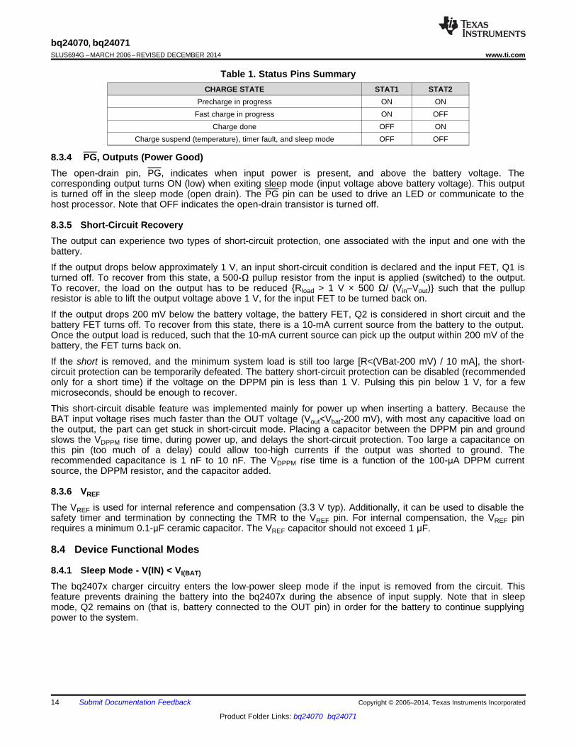
8.3.3 Charge Status OutputsThe open-drain (OD) STAT1 and STAT2 outputs indicate various charger operations as shown in Table 1. Thesestatus pins can be used to drive LEDs or communicate to the host processor. Note that OFF indicates the open-drain transistor is turned off. Note that OFF assumes CE = High.
Copyright © 2006–2014, Texas Instruments Incorporated Submit Documentation Feedback 13
Product Folder Links: bq24070 bq24071
bq24070, bq24071SLUS694G –MARCH 2006–REVISED DECEMBER 2014 www.ti.com
Table 1. Status Pins SummaryCHARGE STATE STAT1 STAT2
Precharge in progress ON ONFast charge in progress ON OFF
Charge done OFF ONCharge suspend (temperature), timer fault, and sleep mode OFF OFF
8.3.4 PG, Outputs (Power Good)The open-drain pin, PG, indicates when input power is present, and above the battery voltage. Thecorresponding output turns ON (low) when exiting sleep mode (input voltage above battery voltage). This outputis turned off in the sleep mode (open drain). The PG pin can be used to drive an LED or communicate to thehost processor. Note that OFF indicates the open-drain transistor is turned off.
8.3.5 Short-Circuit RecoveryThe output can experience two types of short-circuit protection, one associated with the input and one with thebattery.
If the output drops below approximately 1 V, an input short-circuit condition is declared and the input FET, Q1 isturned off. To recover from this state, a 500-Ω pullup resistor from the input is applied (switched) to the output.To recover, the load on the output has to be reduced Rload > 1 V × 500 Ω/ (Vin–Vout) such that the pullupresistor is able to lift the output voltage above 1 V, for the input FET to be turned back on.
If the output drops 200 mV below the battery voltage, the battery FET, Q2 is considered in short circuit and thebattery FET turns off. To recover from this state, there is a 10-mA current source from the battery to the output.Once the output load is reduced, such that the 10-mA current source can pick up the output within 200 mV of thebattery, the FET turns back on.
If the short is removed, and the minimum system load is still too large [R<(VBat-200 mV) / 10 mA], the short-circuit protection can be temporarily defeated. The battery short-circuit protection can be disabled (recommendedonly for a short time) if the voltage on the DPPM pin is less than 1 V. Pulsing this pin below 1 V, for a fewmicroseconds, should be enough to recover.
This short-circuit disable feature was implemented mainly for power up when inserting a battery. Because theBAT input voltage rises much faster than the OUT voltage (Vout<Vbat-200 mV), with most any capacitive load onthe output, the part can get stuck in short-circuit mode. Placing a capacitor between the DPPM pin and groundslows the VDPPM rise time, during power up, and delays the short-circuit protection. Too large a capacitance onthis pin (too much of a delay) could allow too-high currents if the output was shorted to ground. Therecommended capacitance is 1 nF to 10 nF. The VDPPM rise time is a function of the 100-μA DPPM currentsource, the DPPM resistor, and the capacitor added.
8.3.6 VREF
The VREF is used for internal reference and compensation (3.3 V typ). Additionally, it can be used to disable thesafety timer and termination by connecting the TMR to the VREF pin. For internal compensation, the VREF pinrequires a minimum 0.1-μF ceramic capacitor. The VREF capacitor should not exceed 1 μF.
8.4 Device Functional Modes
8.4.1 Sleep Mode - V(IN) < VI(BAT)
The bq2407x charger circuitry enters the low-power sleep mode if the input is removed from the circuit. Thisfeature prevents draining the battery into the bq2407x during the absence of input supply. Note that in sleepmode, Q2 remains on (that is, battery connected to the OUT pin) in order for the battery to continue supplyingpower to the system.
14 Submit Documentation Feedback Copyright © 2006–2014, Texas Instruments Incorporated
Product Folder Links: bq24070 bq24071

bq24070, bq24071www.ti.com SLUS694G –MARCH 2006–REVISED DECEMBER 2014
Device Functional Modes (continued)8.4.2 Standy Mode - V(IN) > VI(BAT)and CE (Chip Enable) Pin = LowThe CE (chip enable) digital input is used to disable or enable the IC. A high-level signal on this pin enables thechip, and a low-level signal disables the device and initiates the standby mode. The bq2407x enters the low-power standby mode when the CE input is low with input present. In this suspend mode, internal power FET Q1(see Figure 3) is turned off; the battery (BAT pin) is used to power the system through Q2 and the OUT pin. Thisfeature is designed to limit the power drawn from the input supply (such as USB suspend mode).
8.4.3 Battery Charge Mode - V(IN) > VI(BAT), Battery Present, CE pin = High and DPPM Pin Not Floating
8.4.3.1 Automous Power Selection and Boot-Up Sequence
The MODE control pin selects the priority of the input sources. If an input source is not available, the battery isselected as the source. With the MODE pin high, the bq2407x charges from the input at the charge rate set bythe ISET1 pin. With the MODE pin low, the bq2407x defaults to the USB charging at the charge rate, and thesupply current is limited by the ISET2 pin (100 mA for ISET2 = Low, 500 mA for ISET2 = High). This featureallows the use of a single connector (mini-USB cable), where the host programs the MODE pin according to thesource that is connected (AC adaptor or USB port). Table 2 summarizes the MODE pin function.
Table 2. Power Source Selection Function SummaryMODE STATE AC MAXIMUM SYSTEM USB BOOT-UP
ADAPTER CHARGE RATE (1) POWER FEATURESOURCE
Low Present ISET2 USB EnabledAbsent N/A Battery Disabled
High Present ISET1 IN DisabledAbsent N/A Battery Disabled
(1) Battery charge rate is always set by ISET1, but may be reduced by a limited input source (ISET2 USB mode) and IOUT system load.
With Mode= Low, in order to facilitate the system start-up and USB enumeration, the bq2407x offers aproprietary boot-up sequence. On the first application of power to the bq2407x, this feature enables the 100-mAUSB charge rate for a period of approximately 150 ms, (t(BOOT-UP)), ignoring the ISET2 and CE inputs setting.At the end of this period, the bq2407x implement CE and ISET2 input settings. See Figure 9.
V(OUT) is regulated to VO(OUT-REG) as long as the the system load, I(SYS), plus the battery charge current, IO(BAT),set by ISET1 does not exceed the maximum input current of
IIN = 2 A if MODE is high orIIN set by ISET2 if MODE is low.
If V(OUT) drops to the DPPM pin preset value, V(DPPM) × SF, due to a limited amount of input current, then thebattery charging current is dynamically reduced until the output voltage stops dropping. If the system demandsmore current than the input can provide, the output voltage drops just below the battery voltage and Q2 turns onwhich allows the battery to supplement the input current to the system. The DPPM circuity is explained in detailin Power-Path Management. The following sections explain the battery charge process in detail. Floating theDPPM pin disables battery charging.
Copyright © 2006–2014, Texas Instruments Incorporated Submit Documentation Feedback 15
Product Folder Links: bq24070 bq24071
Vcc > VI(BAT)checked at all
V I(BAT) < V(LOWV) Yes
No
t(PRECHG)
Expired?
No
Yes
Indicate Fault
Yes
No
Yes
t (CHG)
Expired?
No
Indicate Charge−
In−Progress
Regulate
IO(PRECHG)
Indicate Charge−
In−Progress
Regulate Currentor Voltage
No
Reset and Startt(PRECHG) timer
POR
Yes
Reset all timers,Start t (CHG) timer
No
Yes
V I(BAT) < V(RCH)
?
No
V I(BAT) <V(LOWV)
No
Fault Condition
Yes
Yes
Indicate DONE
T urn off charge
Indicate SLEEP
MODE
SLEEP MODE
V I(BAT) <V(LOWV)
I(TERM)
detection?No
Yes
Yes
V I(BAT) > V(RCH)
?
Enable I(F AUL T)
current
V I(BAT) > V(RCH)
?
No
Yes
Disable I(F AUL T)
current
?
times?
?
bq24070, bq24071SLUS694G –MARCH 2006–REVISED DECEMBER 2014 www.ti.com
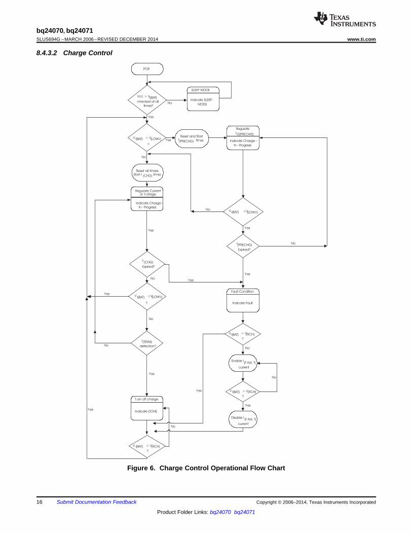
8.4.3.2 Charge Control
Figure 6. Charge Control Operational Flow Chart
16 Submit Documentation Feedback Copyright © 2006–2014, Texas Instruments Incorporated
Product Folder Links: bq24070 bq24071

IO (OUT)
V(SET) K(SET)
RSET
=
×
IO (PRECHG)
V(PRECHG) K(SET)
RSET
=
×
bq24070, bq24071www.ti.com SLUS694G –MARCH 2006–REVISED DECEMBER 2014
8.4.3.3 Battery PreconditioningDuring a charge cycle, if the battery voltage is below the V(LOWV) threshold, the bq2407x applies a prechargecurrent, IO(PRECHG), to the battery. This feature revives deeply discharged cells. The RSET resistor, connectedbetween the ISET1 and VSS pins, determines the precharge rate. The V(PRECHG) and K(SET) parameters arespecified in the specifications table. Note that this applies to both IN-mode and USB-mode charging.
(3)
The bq2407x activates a safety timer, t(PRECHG), during the conditioning phase. If V(LOWV) threshold is not reachedwithin the timer period, the bq2407x turns off the charger and enunciates FAULT on the STAT1 and STAT2 pins.The time-out is extended if the charge current is reduced by DPPM or thermal regulation. See the Timer FaultRecovery section for additional details.
8.4.3.4 Battery Charge CurrentThe bq2407x offers on-chip current regulation with programmable set point. The RSET resistor, connectedbetween the ISET1 and VSS pins, determines the charge level. The charge level may be reduced to give thesystem priority on input current (see DPPM). The V(SET) and K(SET) parameters are specified in the specificationstable.
(4)
When powered from a USB port, the input current available (0.1 A/0.5 A) is typically less than the programmed(ISET1) charging current, and therefore, the DPPM feature attempts to keep the output from being pulled downby reducing the charging current.
The charge level, during IN mode operation only (Mode = High), can be changed by a factor of 2 by setting theISET2 pin high (full charge) or low (half charge). The voltage on the ISET1 pin, VSET1, is divided by 2 when inthe half constant current charge mode. Note that with Mode low, the ISET2 pin controls only the 0.1 A/0.5 A USBcurrent level.
See Power-Path Management for additional details.
8.4.3.5 Battery Voltage RegulationThe voltage regulation feedback is through the BAT pin. This input is tied directly to the positive side of thebattery pack. The bq2407x monitors the battery-pack voltage between the BAT and VSS pins. When the batteryvoltage rises to the VO(REG) threshold, the voltage regulation phase begins and the charging current begins totaper down.
If the battery is absent, the BAT pin cycles between charge done (VO(REG)) and charging (battery rechargethreshold, approximately 4.1 V).
See Figure 8 for power up by battery insertion.
As a safety backup, the bq2407x also monitors the charge time in the charge mode. If charge is not terminatedwithin this time period, t(CHG), the bq2407x turns off the charger and enunciates FAULT on the STAT1 andSTAT2 pins. See the DPPM operation under Case 1 for information on extending the safety timer during DPPMoperation. See the Timer Fault Recovery section for additional details.
8.4.3.6 Temperature Regulation and Thermal ProtectionTo maximize charge rate, the bq2407x features a junction temperature regulation loop. If the power dissipation ofthe IC results in a junction temperature greater than the TJ(REG) threshold, the bq2407x throttles back on thecharge current to maintain a junction temperature around the TJ(REG) threshold. To avoid false termination, thetermination detect function is disabled while in this mode.
The bq2407x also monitors the junction temperature, TJ, of the die and disconnects the OUT pin from the INinput if TJ exceeds T(SHTDWN). This operation continues until TJ falls below T(SHTDWN) by the hysteresis levelspecified in the specification table.
Copyright © 2006–2014, Texas Instruments Incorporated Submit Documentation Feedback 17
Product Folder Links: bq24070 bq24071

V(SET−TREG)
I(OUT) R(SET)
K(SET)
=
×
t(CHG−TREG)
t(CHG) V(SET)
V(SET REG)
=
×
–
t(CHG) K(TMR) R(TMR)= ×
bq24070, bq24071SLUS694G –MARCH 2006–REVISED DECEMBER 2014 www.ti.com
The battery supplement mode has no thermal protection. The Q2 FET continues to connect the battery to theoutput (system), if input power is not sufficient; however, a short-circuit protection circuit limits the batterydischarge current such that the maximum power dissipation of the part is not exceeded under typical designconditions.
8.4.3.7 Charge Timer OperationAs a safety backup, the bq2407x monitors the charge time in the charge mode. If the termination threshold is notdetected within the time period, t(CHG), the bq2407x turns off the charger and enunciates FAULT on the STAT1and STAT2 pins. The resistor connected between the TMR and VSS, RTMR, determines the timer period. TheK(TMR) parameter is specified in the specifications table. In order to disable the charge timer, eliminate RTMR,connect the TMR pin directly to the VREF pin. Note that this action eliminates the fast-charge safety timer (it doesnot disable or reset the precharge safety timer), and also clears any timer fault. TMR pin should not be leftfloating.
(5)
While in the thermal regulation mode or DPPM mode, the bq2407x dynamically adjusts the timer period in orderto provide the additional time needed to fully charge the battery. This proprietary feature is designed to preventagainst early or false termination. The maximum charge time in this mode, t(CHG-TREG), is calculated byEquation 6.
(6)
Note that because this adjustment is dynamic and changes as the ambient temperature changes and the chargelevel changes, the timer clock is adjusted. It is difficult to estimate a total safety time without integrating theabove equation over the charge cycle. Therefore, understanding the theory that the safety time is adjustedinversely proportionately with the charge current and the battery is a current-hour rating, the safety timedynamically adjusts appropriately.
The V(SET) parameter is specified in the specifications table. V(SET-TREG) is the voltage on the ISET pin during thethermal regulation or DPPM mode and is a function of charge current. (Note that charge current is dynamicallyadjusted during the thermal regulation or DPPM mode.)
(7)
All deglitch times also adjusted proportionally to t(CHG-TREG).
8.4.3.8 Timer Fault RecoveryAs shown in Figure 6, bq2407x provides a recovery method to deal with timer fault conditions. The followingsummarizes this method:
Condition 1: Charge voltage above recharge threshold (V(RCH)) and time-out fault occurs.
Recovery Method: bq2407x waits for the battery voltage to fall below the recharge threshold. This could happenas a result of a load on the battery, self-discharge, or battery removal. Once the battery falls below the rechargethreshold, the bq2407x clears the fault and starts a new charge cycle. A POR or CE toggle also clears the fault.
Condition 2: Charge voltage below recharge threshold (V(RCH)) and time-out fault occurs.
Recovery Method: Under this scenario, the bq2407x applies the I(FAULT) current. This small current is used todetect a battery removal condition and remains on as long as the battery voltage stays below the rechargethreshold. If the battery voltage goes above the recharge threshold, then the bq2407x disables the I(FAULT) currentand executes the recovery method described for condition 1. Once the battery falls below the recharge threshold,the bq2407x clears the fault and starts a new charge cycle. A POR or CE toggle also clears the fault.
18 Submit Documentation Feedback Copyright © 2006–2014, Texas Instruments Incorporated
Product Folder Links: bq24070 bq24071

I(TERM)
V(TERM) K(SET)
RSET
=
×
bq24070, bq24071www.ti.com SLUS694G –MARCH 2006–REVISED DECEMBER 2014
8.4.3.9 Charge Termination and RechargeThe bq2407x monitors the voltage on the ISET1 pin, during voltage regulation, to determine when terminationshould occur. Termination occurs when the charge current tapers down to either 1/10th of the programmed fastcharge rate (when the MODE pin is high) or 1/25th of the programmed fast charge rate (when the MODE pin islow). Once the termination threshold, I(TERM), is detected the bq2407x terminates charge. The RSET resistor,connected between the ISET1 and VSS pins, programs the fast charge current level and thus the currenttermination threshold level. The V(TERM) and K(SET) parameters are specified in the specifications table. Note thatthis applies to both IN and USB charging.
(8)
After charge termination, the bq2407x re-starts the charge once the voltage on the BAT pin falls below the V(RCH)threshold. This feature keeps the battery at full capacity at all times.
Copyright © 2006–2014, Texas Instruments Incorporated Submit Documentation Feedback 19
Product Folder Links: bq24070 bq24071

bq24070, bq24071SLUS694G –MARCH 2006–REVISED DECEMBER 2014 www.ti.com
9 Application and Implementation
NOTEInformation in the following applications sections is not part of the TI componentspecification, and TI does not warrant its accuracy or completeness. TI’s customers areresponsible for determining suitability of components for their purposes. Customers shouldvalidate and test their design implementation to confirm system functionality.
9.1 Application InformationCompared to chargers without dynamic power path management (DPPM), this single-cell LiIon battery chargerprovides instant system power even with a deeply discharged battery. The maximum charge current is set byISET2 but the input current limit circuitry, controlled by ISET1 and MODE pins or the DPPM circuitry can reducethe charge current from the maximum desired value.
9.2 Typical Application
Figure 7. Typical Application Circuit
9.2.1 Design RequirementsA bq24070 (VOUT = 4.4 Vreg) is powered through an AC adaptor with IN input is set for approximately 5.1 V (1.5 Acurrent limit), I(CHG) = 1 A, V(DPPM-SET) = 3.7 V, V(DPPM-REG) = 1.15 × V(DPPM-SET) = 4.26 V, Mode = H, and USBinput is not connected. A 103AT thermistor is inside the battery pack. A 6-hour saftey time-out is desired.
20 Submit Documentation Feedback Copyright © 2006–2014, Texas Instruments Incorporated
Product Folder Links: bq24070 bq24071

bq24070, bq24071www.ti.com SLUS694G –MARCH 2006–REVISED DECEMBER 2014
Typical Application (continued)9.2.2 Detailed Design ProcedureThe minimum required 0.1 μF capacitors are placed on IN and OUT. Additional 10-μF capacitors are included onIN and OUT to improve load transient response. The recommended (but not required) 33-μF capacitor on BAT isadded to allow for operation when no battery is attached. A 0.22-μF capacitor is connected between BAT andISET1 to improve operation at low charge currents.
Rearranging Equation 4 gives RSET = V(SET) x K(SET) / IO(BAT) = 2.5 V x 425 / 1 A = 1062.5 Ω → 1070 Ω. PerEquation 3, the precharge current is 100 mA and per Equation 8, the termination current is 100 mA. Since MODEis high, in order to prevent the charge current from being reduced by 1/2, ISET2 is tied high.
Rearranging Equation 5 gives RTMR = t(CHG) / K(TMR) gives 6 hrs x 60 min/hr x 60 s/min / 0.360 s/Ω = 60 kΩ →60.4 kΩ
Rearranging Equation 1 gives RDPPM = V(DPPM-REG) / (I(DPPM) x SF) = 4.26 V / ( 100 μA x 1.15) = 37.044 kΩ →37.4kΩ. CDPPM of 10 nF was added to prevent the IC from falsely entering short circuit protection at start-up.
Not shown are 1.5-kΩ resistors and LEDs pulled up to V(IN) from STAT1, STAT2, and PG.
9.2.2.1 Selecting the Input and Output CapacitorsIn most applications, all that is needed is a high-frequency decoupling capacitor on the input. A 0.1-μF ceramiccapacitor placed in close proximity to the IN to VSS pins works well. In some applications, depending on thepower-supply characteristics and cable length, adding an additional 4.7-μF to 10-μF ceramic capacitor to theinput might be required.
The bq2407x requires only a small output capacitor for loop stability. A 0.1-μF ceramic capacitor placed betweenthe OUT and VSS pin is typically sufficient. TI recommends installing at least an additional 10-uF ceramiccapacitor between OUT and VSS in order to improve load transient response.
TI recommends installing a minimum 33-μF capacitor between the BAT pin and VSS (in parallel with the battery).This configuration ensures proper hot-plug power up with a no-load condition (no system load or batteryattached).
VREF output capacitor with a value of 0.1 μF is required. A 0.22-μF capacitor connected between BAT and ISET1is recommended to improve operation at low charge currents.
This short-circuit disable feature was implemented mainly for power up when inserting a battery. Because theBAT input voltage rises much faster than the OUT voltage (Vout<Vbat-200 mV), with most any capacitive load onthe output, the part can get stuck in short-circuit mode. Placing a 1-nF to 100-nF capacitor between the DPPMpin and ground slows the VDPPM rise time, during power up, and delays the short-circuit protection.
Copyright © 2006–2014, Texas Instruments Incorporated Submit Documentation Feedback 21
Product Folder Links: bq24070 bq24071

T = 4.26 V, DPPM Mode
Reg. @ 4.4 V (bq24070)
VOUT
VAC
ICHG
IOUT
VOUT
VDPPM − OU
VOUT ≈ V ,OUT BAT Supplement Mode
VBAT
VOUT
VAC
IUSB
bq24070, bq24071SLUS694G –MARCH 2006–REVISED DECEMBER 2014 www.ti.com
Typical Application (continued)9.2.3 Application Curves
Figure 9. USB Boot-Up Power-UpFigure 8. Insert Battery – Power-Up Output through BAT
Figure 10. DPPM and Battery Supplement Modes
22 Submit Documentation Feedback Copyright © 2006–2014, Texas Instruments Incorporated
Product Folder Links: bq24070 bq24071

bq24070, bq24071www.ti.com SLUS694G –MARCH 2006–REVISED DECEMBER 2014
10 Power Supply Recommendations
A power supply capable of providing VCC between 4.35 V and 16 V and at least 100 mA up to 2 A is required forthe IC to operate. For the battery to fully charge, the power supply must be capable of providing at least VO(BAT-REG) + V(BATDO). As the input voltage increases, the IC's power dissipation increases. The thermal protection loopof the IC, as explained in Temperature Regulation and Thermal Protection, reduces the input current current fromthe maximum (2 A when MODE = H and either 100 mA or 500 mA per ISET2 if MODE = L) to prevent damage tothe IC.
11 Layout
11.1 Layout Guidelines• For optimal performance, place the decoupling capacitor from the input terminal to VSS and the output filter
capacitor from OUT to VSS as close as possible to the bq2407x, with short trace runs to both signal and VSSpins.
• Keep all low-current VSS connections separate from the high-current charge or discharge paths from thebattery. Use a single-point ground technique incorporating the small signal ground path and the power groundpath.
• The high-current charge paths into IN and from the BAT and OUT pins must be sized appropriately for themaximum charge current to avoid voltage drops in these traces.
• The bq2407x is packaged in a thermally enhanced MLP package. The MLP package includes a QFN thermalpad to provide an effective thermal contact between the device and the printed-circuit board (PCB). Fordetailed PCB design guidelines for this package, see the QFN/SON PCB Attachment Application Note(SLUA271).
The recommend layout is shown in Figure 11.
11.2 Layout Example
Figure 11. Recommended Layout
Copyright © 2006–2014, Texas Instruments Incorporated Submit Documentation Feedback 23
Product Folder Links: bq24070 bq24071

P VIN VOUT IOUT IBAT
VOUT VBAT IBAT
JATJ TA
P
bq24070, bq24071SLUS694G –MARCH 2006–REVISED DECEMBER 2014 www.ti.com
11.3 Thermal ConsiderationsThe bq2407x is packaged in a thermally enhanced MLP package. The package includes a QFN thermal pad toprovide an effective thermal contact between the device and the printed-circuit board (PCB). Full PCB designguidelines for this package are provided in the application note entitled QFN/SON PCB Attachment (SLUA271).The power pad should be tied to the VSS plane. The most common measure of package thermal performance isthermal impedance (θJA) measured (or modeled) from the chip junction to the air surrounding the packagesurface (ambient).
The mathematical expression for θJA is:
where• TJ = chip junction temperature• TA = ambient temperature• P = device power dissipation (9)
Factors that can greatly influence the measurement and calculation of θJA include:• whether or not the device is board mounted• trace size, composition, thickness, and geometry• orientation of the device (horizontal or vertical)• volume of the ambient air surrounding the device under test and airflow• whether other surfaces are in close proximity to the device being tested
The device power dissipation, P, is a function of the charge rate and the voltage drop across the internal powerFET. It can be calculated from Equation 10:
(10)
Due to the charge profile of Li-xx batteries, the maximum power dissipation is typically seen at the beginning ofthe charge cycle when the battery voltage is at its lowest. See Figure 2. Typically the voltage of the Li-ion batteryquickly (< 2 V minutes) ramps to approximately 3.5 V, when entering fast charge (1-C charge rate and batteryabove 3 V). Therefore, it is customary to perform the steady-state thermal design using 3.5 V as the minimumbattery voltage because the system board and charging device does not have time to reach a maximumtemperature due to the thermal mass of the assembly during the early stages of fast charge. This theory is easilyverified by performing a charge cycle on a discharged battery while monitoring the battery voltage and chargerspower pad temperature.
24 Submit Documentation Feedback Copyright © 2006–2014, Texas Instruments Incorporated
Product Folder Links: bq24070 bq24071

bq24070, bq24071www.ti.com SLUS694G –MARCH 2006–REVISED DECEMBER 2014
12 Device and Documentation Support
12.1 Documentation Support
12.1.1 Related DocumentationFor related documentation, see the following:• QFN/SON PCB Attachment Application Note (SLUA271)
12.2 Related LinksThe table below lists quick access links. Categories include technical documents, support and communityresources, tools and software, and quick access to sample or buy.
Table 3. Related LinksTECHNICAL TOOLS & SUPPORT &PARTS PRODUCT FOLDER SAMPLE & BUY DOCUMENTS SOFTWARE COMMUNITY
bq24070 Click here Click here Click here Click here Click herebq24071 Click here Click here Click here Click here Click here
12.3 TrademarksAll trademarks are the property of their respective owners.
12.4 Electrostatic Discharge CautionThese devices have limited built-in ESD protection. The leads should be shorted together or the device placed in conductive foamduring storage or handling to prevent electrostatic damage to the MOS gates.
12.5 GlossarySLYZ022 — TI Glossary.
This glossary lists and explains terms, acronyms, and definitions.
13 Mechanical, Packaging, and Orderable Information
The following pages include mechanical, packaging, and orderable information. This information is the mostcurrent data available for the designated devices. This data is subject to change without notice and revision ofthis document. For browser-based versions of this data sheet, refer to the left-hand navigation.
Copyright © 2006–2014, Texas Instruments Incorporated Submit Documentation Feedback 25
Product Folder Links: bq24070 bq24071

PACKAGE OPTION ADDENDUM
www.ti.com 24-Aug-2018
Addendum-Page 1
PACKAGING INFORMATION
Orderable Device Status(1)
Package Type PackageDrawing
Pins PackageQty
Eco Plan(2)
Lead/Ball Finish(6)
MSL Peak Temp(3)
Op Temp (°C) Device Marking(4/5)
Samples
BQ24070RHLR ACTIVE VQFN RHL 20 3000 Green (RoHS& no Sb/Br)
CU NIPDAU Level-2-260C-1 YEAR -40 to 85 BRQ
BQ24070RHLT ACTIVE VQFN RHL 20 250 Green (RoHS& no Sb/Br)
CU NIPDAU Level-2-260C-1 YEAR -40 to 85 BRQ
BQ24070RHLTG4 ACTIVE VQFN RHL 20 250 Green (RoHS& no Sb/Br)
CU NIPDAU Level-2-260C-1 YEAR -40 to 85 BRQ
BQ24071RHLR ACTIVE VQFN RHL 20 3000 Green (RoHS& no Sb/Br)
CU NIPDAU Level-2-260C-1 YEAR -40 to 85 BTR
BQ24071RHLT ACTIVE VQFN RHL 20 250 Green (RoHS& no Sb/Br)
CU NIPDAU Level-2-260C-1 YEAR -40 to 85 BTR
(1) The marketing status values are defined as follows:ACTIVE: Product device recommended for new designs.LIFEBUY: TI has announced that the device will be discontinued, and a lifetime-buy period is in effect.NRND: Not recommended for new designs. Device is in production to support existing customers, but TI does not recommend using this part in a new design.PREVIEW: Device has been announced but is not in production. Samples may or may not be available.OBSOLETE: TI has discontinued the production of the device.
(2) RoHS: TI defines "RoHS" to mean semiconductor products that are compliant with the current EU RoHS requirements for all 10 RoHS substances, including the requirement that RoHS substancedo not exceed 0.1% by weight in homogeneous materials. Where designed to be soldered at high temperatures, "RoHS" products are suitable for use in specified lead-free processes. TI mayreference these types of products as "Pb-Free".RoHS Exempt: TI defines "RoHS Exempt" to mean products that contain lead but are compliant with EU RoHS pursuant to a specific EU RoHS exemption.Green: TI defines "Green" to mean the content of Chlorine (Cl) and Bromine (Br) based flame retardants meet JS709B low halogen requirements of <=1000ppm threshold. Antimony trioxide basedflame retardants must also meet the <=1000ppm threshold requirement.
(3) MSL, Peak Temp. - The Moisture Sensitivity Level rating according to the JEDEC industry standard classifications, and peak solder temperature.
(4) There may be additional marking, which relates to the logo, the lot trace code information, or the environmental category on the device.
(5) Multiple Device Markings will be inside parentheses. Only one Device Marking contained in parentheses and separated by a "~" will appear on a device. If a line is indented then it is a continuationof the previous line and the two combined represent the entire Device Marking for that device.
(6) Lead/Ball Finish - Orderable Devices may have multiple material finish options. Finish options are separated by a vertical ruled line. Lead/Ball Finish values may wrap to two lines if the finishvalue exceeds the maximum column width.

PACKAGE OPTION ADDENDUM
www.ti.com 24-Aug-2018
Addendum-Page 2
Important Information and Disclaimer:The information provided on this page represents TI's knowledge and belief as of the date that it is provided. TI bases its knowledge and belief on informationprovided by third parties, and makes no representation or warranty as to the accuracy of such information. Efforts are underway to better integrate information from third parties. TI has taken andcontinues to take reasonable steps to provide representative and accurate information but may not have conducted destructive testing or chemical analysis on incoming materials and chemicals.TI and TI suppliers consider certain information to be proprietary, and thus CAS numbers and other limited information may not be available for release.
In no event shall TI's liability arising out of such information exceed the total purchase price of the TI part(s) at issue in this document sold by TI to Customer on an annual basis.
TAPE AND REEL INFORMATION
*All dimensions are nominal
Device PackageType
PackageDrawing
Pins SPQ ReelDiameter
(mm)
ReelWidth
W1 (mm)
A0(mm)
B0(mm)
K0(mm)
P1(mm)
W(mm)
Pin1Quadrant
BQ24070RHLR VQFN RHL 20 3000 330.0 12.4 3.8 4.8 1.6 8.0 12.0 Q1
BQ24070RHLR VQFN RHL 20 3000 330.0 12.4 3.8 4.8 1.3 8.0 12.0 Q1
BQ24070RHLT VQFN RHL 20 250 180.0 12.4 3.8 4.8 1.3 8.0 12.0 Q1
BQ24070RHLT VQFN RHL 20 250 180.0 12.4 3.8 4.8 1.6 8.0 12.0 Q1
BQ24071RHLR VQFN RHL 20 3000 330.0 12.4 3.8 4.8 1.6 8.0 12.0 Q1
BQ24071RHLT VQFN RHL 20 250 180.0 12.4 3.8 4.8 1.6 8.0 12.0 Q1
PACKAGE MATERIALS INFORMATION
www.ti.com 9-Mar-2018
Pack Materials-Page 1

*All dimensions are nominal
Device Package Type Package Drawing Pins SPQ Length (mm) Width (mm) Height (mm)
BQ24070RHLR VQFN RHL 20 3000 367.0 367.0 35.0
BQ24070RHLR VQFN RHL 20 3000 370.0 355.0 55.0
BQ24070RHLT VQFN RHL 20 250 195.0 200.0 45.0
BQ24070RHLT VQFN RHL 20 250 210.0 185.0 35.0
BQ24071RHLR VQFN RHL 20 3000 367.0 367.0 35.0
BQ24071RHLT VQFN RHL 20 250 210.0 185.0 35.0
PACKAGE MATERIALS INFORMATION
www.ti.com 9-Mar-2018
Pack Materials-Page 2

NOTES:
1. All linear dimensions are in millimeters. Any dimensions in parenthesis are for reference only. Dimensioning and tolerancingper ASME Y14.5M.
2. This drawing is subject to change without notice.3. The package thermal pad must be soldered to the printed circuit board for thermal and mechanical performance.
PACKAGE OUTLINE
4219071 / A 05/2017
www.ti.com
VQFN - 1 mm max height
PLASTIC QUAD FLATPACK- NO LEAD
RHL0020A
A
0.08 C
0.1 C A B0.05 C
B
SYMM
SYMM
PIN 1 INDEX AREA
SEATING PLANE
C
1PIN 1 ID(OPTIONAL)
2.05±0.1
3.05±0.1
3.63.4
4.64.4
1 MAX
(0.2) TYP
2X (0.55)
2X3.5
14X 0.5
2
9
10 11
12
19
20
2X 1.5
4X (0.2)
20X 0.290.19
20X 0.50.3
21

NOTES: (continued)
4. This package is designed to be soldered to a thermal pad on the board. For more information, see Texas Instrumentsliterature number SLUA271 (www.ti.com/lit/slua271) .
5. Solder mask tolerances between and around signal pads can vary based on board fabrication site.6. Vias are optional depending on application, refer to device data sheet. If any vias are implemented, refer to theri
locations shown on this view. It is recommended that vias under paste be filled, plugged or tented.
EXAMPLE BOARD LAYOUT
4219071 / A 05/2017
www.ti.com
VQFN - 1 mm max height
RHL0020A
PLASTIC QUAD FLATPACK- NO LEAD
SYMM
SYMM
LAND PATTERN EXAMPLEEXPOSED METAL SHOWN
SCALE: 18X
2X (1.5)
6X (0.525)
4X(0.775)
(4.3)
(3.3)
20X (0.6)
20X (0.24)
14X (0.5)
(3.05)
(2.05)
(R0.05) TYP
(Ø0.2) VIATYP)
1
2
9
10 11
12
19
20
0.07 MAXALL AROUND 0.07 MIN
ALL AROUND
SOLDER MASK DETAILS
NON SOLDER MASKDEFINED
(PREFERRED)
SOLDER MASKDEFINED
METAL
SOLDER MASKOPENING
SOLDER MASKOPENING
METAL UNDERSOLDER MASK
21
2X (0.75)
2X (0.4)
SOLDER MASKOPENING
METAL UNDERSOLDER MASK
4X (0.2)
2X (0.55)
EXPOSED METAL EXPOSED METAL
NOTES: (continued)
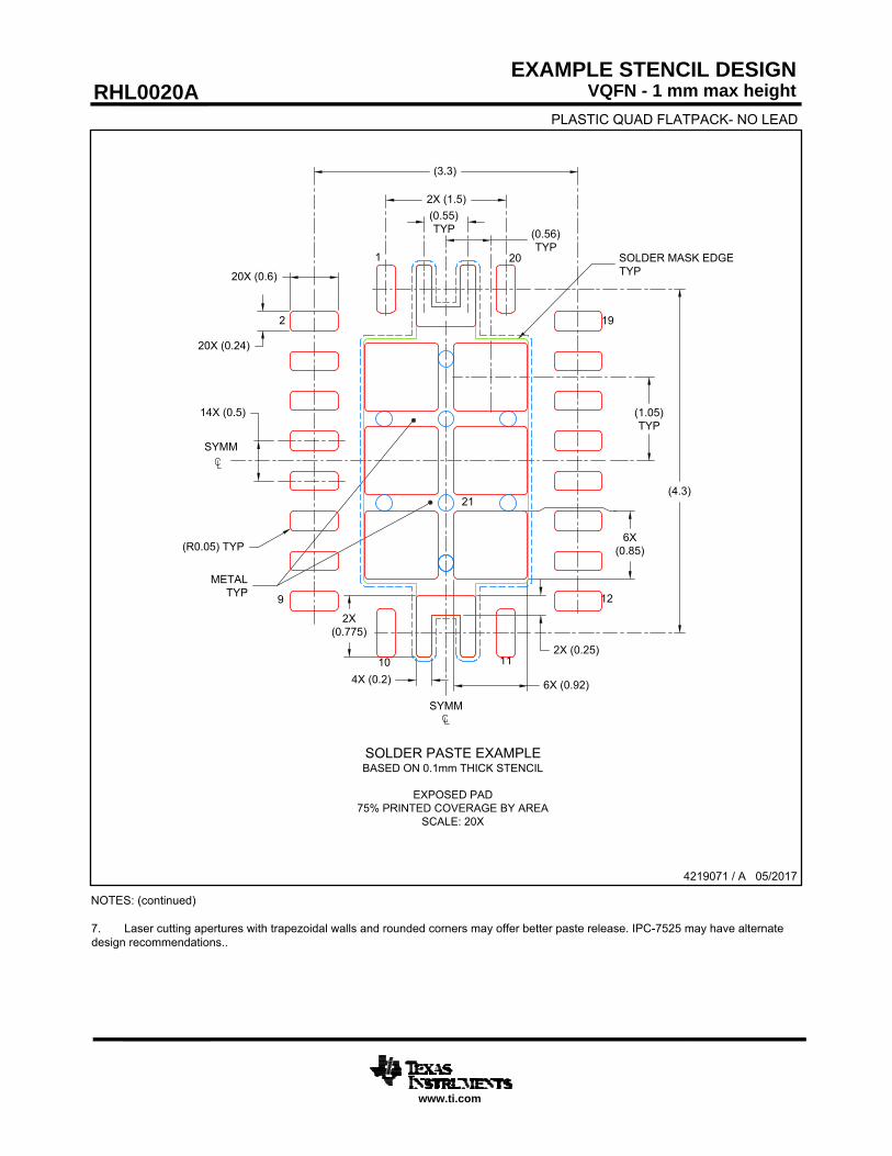
7. Laser cutting apertures with trapezoidal walls and rounded corners may offer better paste release. IPC-7525 may have alternatedesign recommendations..
EXAMPLE STENCIL DESIGN
4219071 / A 05/2017
www.ti.com
VQFN - 1 mm max height
RHL0020A
PLASTIC QUAD FLATPACK- NO LEAD
SYMM
SYMM
SOLDER PASTE EXAMPLEBASED ON 0.1mm THICK STENCIL
EXPOSED PAD75% PRINTED COVERAGE BY AREA
SCALE: 20X
(4.3)
2X (1.5)
(3.3)
(1.05)TYP
6X (0.92)
6X(0.85)
14X (0.5)
20X (0.24)
20X (0.6)
(0.56)TYP
METALTYP
21
4X (0.2)
2X (0.25)
(0.55)TYP
SOLDER MASK EDGETYP
2X(0.775)
1
2
9
10 11
12
19
20
(R0.05) TYP

IMPORTANT NOTICE
Texas Instruments Incorporated (TI) reserves the right to make corrections, enhancements, improvements and other changes to itssemiconductor products and services per JESD46, latest issue, and to discontinue any product or service per JESD48, latest issue. Buyersshould obtain the latest relevant information before placing orders and should verify that such information is current and complete.TI’s published terms of sale for semiconductor products (http://www.ti.com/sc/docs/stdterms.htm) apply to the sale of packaged integratedcircuit products that TI has qualified and released to market. Additional terms may apply to the use or sale of other types of TI products andservices.Reproduction of significant portions of TI information in TI data sheets is permissible only if reproduction is without alteration and isaccompanied by all associated warranties, conditions, limitations, and notices. TI is not responsible or liable for such reproduceddocumentation. Information of third parties may be subject to additional restrictions. Resale of TI products or services with statementsdifferent from or beyond the parameters stated by TI for that product or service voids all express and any implied warranties for theassociated TI product or service and is an unfair and deceptive business practice. TI is not responsible or liable for any such statements.Buyers and others who are developing systems that incorporate TI products (collectively, “Designers”) understand and agree that Designersremain responsible for using their independent analysis, evaluation and judgment in designing their applications and that Designers havefull and exclusive responsibility to assure the safety of Designers' applications and compliance of their applications (and of all TI productsused in or for Designers’ applications) with all applicable regulations, laws and other applicable requirements. Designer represents that, withrespect to their applications, Designer has all the necessary expertise to create and implement safeguards that (1) anticipate dangerousconsequences of failures, (2) monitor failures and their consequences, and (3) lessen the likelihood of failures that might cause harm andtake appropriate actions. Designer agrees that prior to using or distributing any applications that include TI products, Designer willthoroughly test such applications and the functionality of such TI products as used in such applications.TI’s provision of technical, application or other design advice, quality characterization, reliability data or other services or information,including, but not limited to, reference designs and materials relating to evaluation modules, (collectively, “TI Resources”) are intended toassist designers who are developing applications that incorporate TI products; by downloading, accessing or using TI Resources in anyway, Designer (individually or, if Designer is acting on behalf of a company, Designer’s company) agrees to use any particular TI Resourcesolely for this purpose and subject to the terms of this Notice.TI’s provision of TI Resources does not expand or otherwise alter TI’s applicable published warranties or warranty disclaimers for TIproducts, and no additional obligations or liabilities arise from TI providing such TI Resources. TI reserves the right to make corrections,enhancements, improvements and other changes to its TI Resources. TI has not conducted any testing other than that specificallydescribed in the published documentation for a particular TI Resource.Designer is authorized to use, copy and modify any individual TI Resource only in connection with the development of applications thatinclude the TI product(s) identified in such TI Resource. NO OTHER LICENSE, EXPRESS OR IMPLIED, BY ESTOPPEL OR OTHERWISETO ANY OTHER TI INTELLECTUAL PROPERTY RIGHT, AND NO LICENSE TO ANY TECHNOLOGY OR INTELLECTUAL PROPERTYRIGHT OF TI OR ANY THIRD PARTY IS GRANTED HEREIN, including but not limited to any patent right, copyright, mask work right, orother intellectual property right relating to any combination, machine, or process in which TI products or services are used. Informationregarding or referencing third-party products or services does not constitute a license to use such products or services, or a warranty orendorsement thereof. Use of TI Resources may require a license from a third party under the patents or other intellectual property of thethird party, or a license from TI under the patents or other intellectual property of TI.TI RESOURCES ARE PROVIDED “AS IS” AND WITH ALL FAULTS. TI DISCLAIMS ALL OTHER WARRANTIES ORREPRESENTATIONS, EXPRESS OR IMPLIED, REGARDING RESOURCES OR USE THEREOF, INCLUDING BUT NOT LIMITED TOACCURACY OR COMPLETENESS, TITLE, ANY EPIDEMIC FAILURE WARRANTY AND ANY IMPLIED WARRANTIES OFMERCHANTABILITY, FITNESS FOR A PARTICULAR PURPOSE, AND NON-INFRINGEMENT OF ANY THIRD PARTY INTELLECTUALPROPERTY RIGHTS. TI SHALL NOT BE LIABLE FOR AND SHALL NOT DEFEND OR INDEMNIFY DESIGNER AGAINST ANY CLAIM,INCLUDING BUT NOT LIMITED TO ANY INFRINGEMENT CLAIM THAT RELATES TO OR IS BASED ON ANY COMBINATION OFPRODUCTS EVEN IF DESCRIBED IN TI RESOURCES OR OTHERWISE. IN NO EVENT SHALL TI BE LIABLE FOR ANY ACTUAL,DIRECT, SPECIAL, COLLATERAL, INDIRECT, PUNITIVE, INCIDENTAL, CONSEQUENTIAL OR EXEMPLARY DAMAGES INCONNECTION WITH OR ARISING OUT OF TI RESOURCES OR USE THEREOF, AND REGARDLESS OF WHETHER TI HAS BEENADVISED OF THE POSSIBILITY OF SUCH DAMAGES.Unless TI has explicitly designated an individual product as meeting the requirements of a particular industry standard (e.g., ISO/TS 16949and ISO 26262), TI is not responsible for any failure to meet such industry standard requirements.Where TI specifically promotes products as facilitating functional safety or as compliant with industry functional safety standards, suchproducts are intended to help enable customers to design and create their own applications that meet applicable functional safety standardsand requirements. Using products in an application does not by itself establish any safety features in the application. Designers mustensure compliance with safety-related requirements and standards applicable to their applications. Designer may not use any TI products inlife-critical medical equipment unless authorized officers of the parties have executed a special contract specifically governing such use.Life-critical medical equipment is medical equipment where failure of such equipment would cause serious bodily injury or death (e.g., lifesupport, pacemakers, defibrillators, heart pumps, neurostimulators, and implantables). Such equipment includes, without limitation, allmedical devices identified by the U.S. Food and Drug Administration as Class III devices and equivalent classifications outside the U.S.TI may expressly designate certain products as completing a particular qualification (e.g., Q100, Military Grade, or Enhanced Product).Designers agree that it has the necessary expertise to select the product with the appropriate qualification designation for their applicationsand that proper product selection is at Designers’ own risk. Designers are solely responsible for compliance with all legal and regulatoryrequirements in connection with such selection.Designer will fully indemnify TI and its representatives against any damages, costs, losses, and/or liabilities arising out of Designer’s non-compliance with the terms and provisions of this Notice.
Mailing Address: Texas Instruments, Post Office Box 655303, Dallas, Texas 75265Copyright © 2018, Texas Instruments Incorporated