single s1563s/dual s1563d pentium class 430 hx 75mhz thru ... iii - s1563/m...revision 1.0 single...
TRANSCRIPT
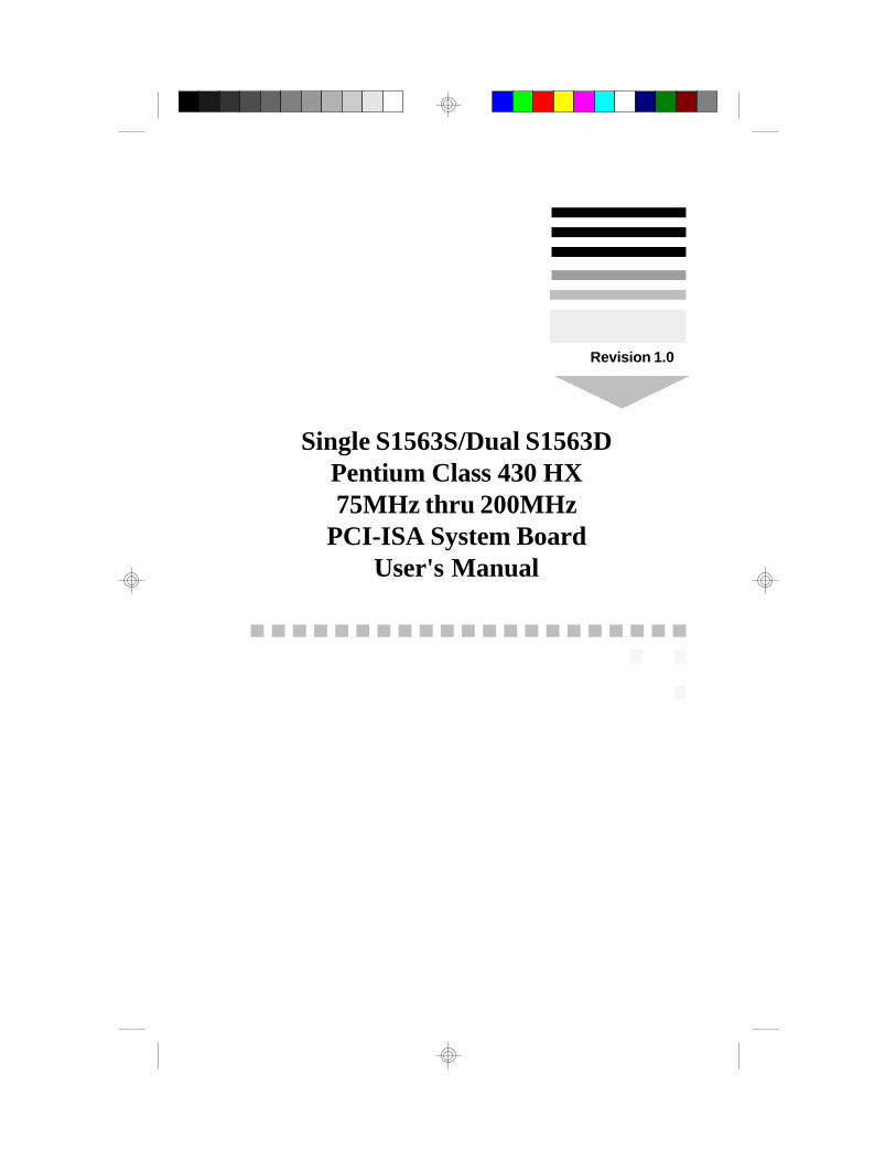
Revision 1.0
Single S1563S/Dual S1563DPentium Class 430 HX75MHz thru 200MHz
PCI-ISA System BoardUser's Manual
2S1563-001-01 www.tyan.com
Table Of Contents
1. Introduction....................................................................... 41.1 Overview................................................................41.2 Hardware Specifications..........................................51.3 Software Specifications.......................................... 61.4 Environment........................................................... 6
2. Board Installation.............................................................. 72.1 Unpacking.............................................................. 72.2 Installation.............................................................. 7
3. S1563On Board Resource Settings................................. 83.1 S1563Board Layout & Jumper Locations................ 83.2 Quick Reference for Jumpers.................................. 93.3 CMOS RTC............................................................133.4 Speaker Connector.................................................. 133.5 Turbo Switch.......................................................... 133.6 Turbo LED Connect................................................ 133.7 Reset Connector..................................................... 143.8 Flash EPROM Jumpers.......................................... 143.9 CMOS & Password Reset...................................... 143.10 DRAM Installation................................................ 153.11 CPU Installation.................................................... 183.12 Cache Memory.................................................... 193.13 Understanding Different Clock Speeds................... 203.14 Peripheral Device Installation................................. 213.15 Connecting The Power Supply...............................22
4. BIOS Configuration...........................................................244.1 Entering Setup....................................................... 244.2 Control Keys......................................................... 254.3 Getting Help........................................................... 264.4 The Main Menu...................................................... 264.5 Standard CMOS Setup Menu...................................284.6 BIOS Features Setup.............................................. 314.7 Chipset Features Setup............................................ 34
4.7.1 Power Management Setup........................ 394.8 PCI Slot Configuration.............................................414.9 Integrated Peripherals............................................. 434.10 Load Setup Defaults.............................................. 44
4.11Password Setting................................................... 444.12 IDE HDD Auto Detection..................................... 464.13 Save & Exit Setup................................................. 464.14 Keyboard Setting Functions....................................47

3S1563-001-01 www.tyan.com
5.AMI WinBIOS....................................................................485.1 Standard Setup Options........................................... 485.2 Advanced Setup..................................................... 495.3 Advanced Chipset.................................................. 525.4 Power Management................................................ 565.5 Peripheral............................................................... 575.6 Utility..................................................................... 585.7 Security.................................................................. 585.8 Defaults................................................................. 58
6. Flash Writer Utility............................................................ 596.1 The Flash Memory Writer Utility Screen...................61
7. Timer &DMA Channel Map............................................. 627.1 Interrupt Map......................................................... 62
Information presented in this publication has been carefully checked forreliability; however, no responsibility is assumed for inaccuracies. Theinformation contained in this document is subject to change withoutnotice.
TrademarksAward BIOS/Flash are trademarks of Award Software International Inc.AMI BIOS is a trademarks of American Megatrends Inc.IBM,PC,AT,PS/2 are trademarks of IBM CorporationINTEL,Pentium are trademarks of Intel Corporation.Cyrix is a trademark of Cyrix Corp.Copyright c 1996 TYAN Computer Corp.Tomcat III, S1563.

4S1563-001-01 www.tyan.com
1. Introduction
1.1 Overview
The S1563D is a quality, high performance dual processor mainboardbased on the powerful Intel Pentium microprocessors. This mainboard isdesigned around the latest and fastest Intel 430HX(II) chipset and cansupport CPU speeds of 75MHz through 200MHz and beyond. TheS1563S is single processor mainboard and the S1563D is a dual processormainboard.
The S1563 supports single or dual Pentium and singleCyrix processors,EDO memory, ECC memory and memory parity checking.The S1563'sPCI Local Bus provides high performance capabilities that are ideal for awide range of demanding applications such as: CAD, CAM, CAE,networking, multi-user environments, database management, desktoppublishing, image processing and 3D animation.
This integrated system board achieves the highest reliability and yet issmall enough for all of its features to be supported in a "Baby-AT" form-factor. Some of the features included are: on-board dual channel PCIIDE, on-board floppy controller, on-board high speed I/O, and support forpipeline-burst SRAM.
Flexibility and expandibility have been designed into the S1563. With I/Oand drive controller support built on-board, the four PCI and five ISA(One ISA and one PCI as a shared slot) slots are free for any add-onexpansion cards. With eight SIMM sockets, the S1563 can provide a veryflexible memory configuration of 8MB to 512MB of RAM. With theS1563D's support for dual Pentium processors, you can start a systemwith just one CPU, and later add another, when more processing power isrequired.
NoticeThis board uses the Intel 430HX chipset. According to Intel , the USBfunction in this chipset is not guaranteed. Compatibility tests cannot beconducted for USB at this time due to no availability of such devicesand drives. Please log on to the Tyan web page for the latest infomation.

5S1563-001-01 www.tyan.com
1.2 Hardware Specifications/Features
wCPU Intel Pentium 75 MHz thru 200 MHz (Socket 7)(Single or Dual CPU configuration)Cyrix 6x86 P120, P150 and P166(Single Only)
wCoprocessor On-chip floating point unit
wSpeed 50/60/66 MHz system bus25/30/33 MHz PCI bus7.5/8.33 MHz ISA bus speed
wDRAM 4 double banks of 72 pin SIMM socketsSupports 5V or 3.3V memorySupports EDO(Exended Data Out) DRAMsSupports ECC(Error Correcting Code)w/ paritySupports Fast Page Mode DRAMsSupports 8MB to 512MB of DRAMs
wL2 Cache 512KB on board 2nd level cache memorySupports synchronous pipeline-burst cache
wEIDE Controller Primary and secondary PCI EIDE channels onboard for support of up to four EIDE Mode 0through Mode 4 drives.Supports DMA(Bus Master) mode 1 and 2.( Bus Master driver on web at www.tyan.com)
wEnhanced I/O Multi-mode bi-directional parallel port thatsupports standard, EPP and ECP modes.Supports 16550 compatible UARTS for on-boardhigh speed serial ports.Support for an IrDA compliant InfraRed inter-face.On-board floppy controller.
wMouse On-board PS/2 mouse connector.
wI/O Bus Slots 4 Master/Slave PCI-Bus5 ISA Bus (One ISA and one PCI shared slot)

6S1563-001-01 www.tyan.com
1.3 Software Specifications
wBIOS Licensed Award or AMI BIOSAT CMOS setup, BIOS/CHIPSET setup,and hard disk utility included.Support for easy BIOS upgrades with flashEEPROM chip.
wO.S. Operates with MS-DOS, Windows 3.x, Windowsfor Work Groups 3.x, Windows 95, Windows NT,OS/2, Novell Netware, Novell UnixWare 1.1 andSCO Unix.
1.4 Environment
Ambient Temperature 0 to +50 C (operating)Relative Humidity 0 to +85% (operating)Altitude 0 to 10,000 feet (operating)Vibration 0 to 1,000 HzVoltage 4.9 to 5.2 V

7S1563-001-01 www.tyan.com
2. Board Installation
2.1 Unpacking
The mainboard package should contain the following:wS1563 MainboardwOne IDE 40 pin cableswTwo serial cableswwOne parallel cablewOne 34 pin floppy cablewUser's Manual
The mainboard contains sensitive electric components which can be easilydamaged by static electricity, so the mainboard should be left in its originalpackaging until it is ready to be installed.
With the power supply pluged in and turned off touch an unpainted area ofthe system chassis imedietly before handling the mainboard or any compo-nent. Doing so discharges the static charge your body may have built.
After opening the mainboard carton, extract the system board holding it byits edges ,and place it only on a grounded anti-static surface, componentside up. Inspect the board for damage. Press down on all of the socket IC'sto make sure that they are properly seated. Do this only with the boardplaced on an anti-static mat. Do not touch the bottom of the board.
DO NOT APPLY POWER TO THE BOARD IF IT HAS BEENDAMAGED!
2.2 Installation
You are now ready to install your mainboard. The mounting hole pattern ofthe S1563 matches the "Baby AT" system board spec. It is assumed thatthe chassis is for a standard IBM XT/AT form factor.

8S1563-001-01 www.tyan.com
PCI
Slot
1
Ban
k 0
Ban
k 0
Ban
k 1
Ban
k 1
PCI
Slot
2
PCI
Slot
4
3. On Board Resource Setting
KB CTRPWR CON. 5V
ISA
Slo
t 1
ISA
Slo
t 2
ISA
Slo
t 3
ISA
Slo
t 4
ISA
Slo
t 5
Ban
k 3
Flop
py C
on.
KeyboardCON
BIO
SA
MI/
AW
AR
D
J48
J28
Para
llel P
ort
J1
PS/2MouseHeader
1
1
1
1
1 1
82039AA
Sock
et 7
CPU 1
82371SB
Sock
et 7
CPU 0
RTC
pin 1
IR2
USB
1
USB
2
J14
PCI
Slot
3
J15
J45
J13
pin 1
pin 1
J29J30J31J32J33J34J35J36
IR1J25
J 2 4J27 J 2 3
J 2 2
J 2 0
J 2 6
pin 1
pin 1J50
J 4 6
pin 1
Seco
ndar
y ID
E
Prim
ary
IDE
Ban
k 2
Ban
k 2
Ban
k 3
Figure 3.1 S1563 Board Layout
Com1
Com2
pin 1
J16 82439HX
J12
J 4 2J 4 3J 4 4J53J52J54
J39
J38
J37
J41
J40
J56
J55
J19
SRA
M
SRA
M
SRA
M
SRA
M
J 9
J10
J2J11
Jumper is open/off
Jumper is closed/onJumpers shown are
defaults
Only on S1563D

9S1563-001-01 www.tyan.com
APIC For DP: J50 (Dual CPU Jumper for S1563D only)
J50Dual CPU 2-3 DefaultSingle CPU 1-2
*Note: When using two Pentiums, Intel recommends that the chips have the same s-spec number. These numbers are stamped on the top and bottom or the Pentium chips. Check with your CPU vendor for more info about s-spec numbers.
3.2 Jumper Settings
CPU Speed: J13 J19 J20 CPU Speed 1-2, 3-4 Off Off 75 MHz
3-4 Off Off 90 MHz1-2 Off Off 100 MHz3-4 On Off 120 MHz Cyrix P150+1-2 On Off 133 MHz Cyrix P166+
3-4 On On 150 MHz1-2 On On 166 MHz1-2 Off On 200 MHz
1-2, 3-4 On Off 100MHz Cyrix P120+
DRAM Voltage Setting:J1, J2, J11, J12, J8, J9, & J10
Damage to system can result if these are set incorrectly!
Volts J1 J2 J11 J12 J8 J9 J10Default 5V On On On On Off Off Off
3.3V Off Off Off Off On On On
CMOS Reset: J46
Off: Normal operation(Default)On: Clears password and resets CMOS
wWith power off, put jumper on J46 for about 10 seconds.wRemove jumper and power system on and the CMOS will be reset.
10S1563-001-01 www.tyan.com
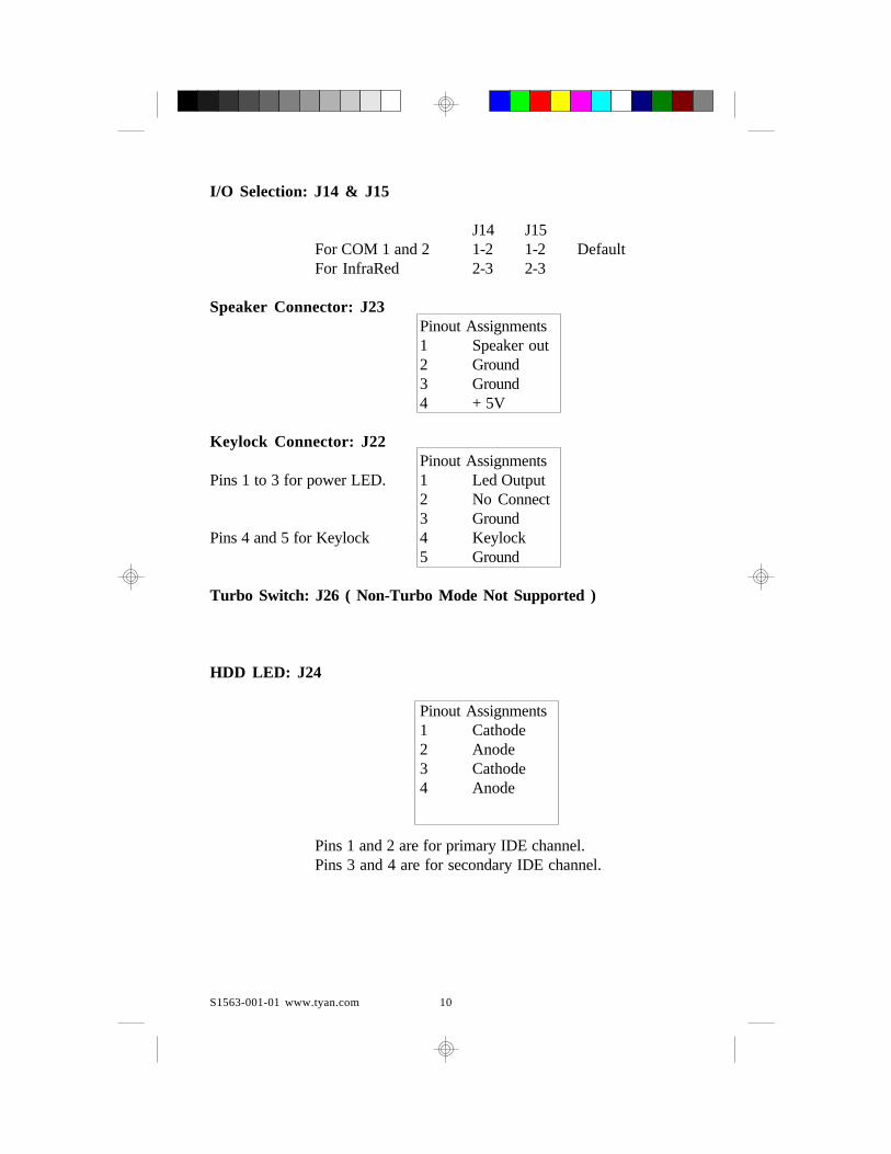
I/O Selection: J14 & J15
J14 J15For COM 1 and 2 1-2 1-2 DefaultFor InfraRed 2-3 2-3
Speaker Connector: J23Pinout Assignments1 Speaker out2 Ground3 Ground4 + 5V
Keylock Connector: J22Pinout Assignments
Pins 1 to 3 for power LED. 1 Led Output2 No Connect3 Ground
Pins 4 and 5 for Keylock 4 Keylock5 Ground
Turbo Switch: J26 ( Non-Turbo Mode Not Supported )
HDD LED: J24
Pinout Assignments1 Cathode2 Anode3 Cathode4 Anode
Pins 1 and 2 are for primary IDE channel.Pins 3 and 4 are for secondary IDE channel.

11S1563-001-01 www.tyan.com
PS/2 Pinout:
Ground Data VCC
Keyboard Connector
ClK
Reset Connector: J27Pinout Assignment1 Power Good2 Ground
Turbo LED Connector: J25Pinout Assignment1 Cathode2 Anode
Flash EEPROM: J48
This jumper should be left at the factory default.
J48 1-2
InfraRed Interface: Con7 and Con9
Pinout Assignment1 Signal In2 Gnd3 Signal Out4 VCC

12S1563-001-01 www.tyan.com
CPU Voltage Regulator Settings:
Pentium MMX requires two voltage sources, J60, J61, & J62 are settings forone source. J63, J64 and J65 are settings for the second voltage source. Thedefault setting is for P54C/Cyrix CPU's.
P54C(Pentium) & Cyrix P55C(Pentium MMX)3.6V 3.5V 3.3V 3.0V 2.85V 2.65V
J39 off on off J42 on off offJ38 on off off J43 off off onJ37 off off on J44 off on offJ40 on J40 offJ41 on J41 offJ42 off J52 off Settings forJ43 off Default settings J53 on P55C onlyJ44 off for P54C and Cyrix J54 onJ52 onJ53 offJ54 off

13S1563-001-01 www.tyan.com
3.3 CMOS RTC
CMOS RTC includes an internal battery and Real Time Clock circuit. Itprovides the date and the time for the system. Normally the life span of aRTC internal battery is 10 years. When replacing, you should use the samemodel.
3.4 Speaker Connector Installation
S1563 provides a 4-Pin header (J23) to connect the speaker. The polaritycan go either way.
3.5 Turbo Switch
The front panel on your case may have a turbo switch to control systemspeed when slower program execution is required for software developedin the old XT days.
The Intel 430HX chipset doesn't support a de-turbo mode, but the S1563has a connector (J26) for the cable that may come with the case.
3.6 Turbo LED Connector Installation
The TURBO LED on the front case panel can indicate the current speedstatus of the system. The TURBO LED connector should be installed toJ25 in the correct direction.

14S1563-001-01 www.tyan.com
3.7 Hardware Reset Switch Connector Installation
The RESET switch on your cases' display panel provides users with theHARDWARE RESET function which is the same as power on/off. Thesystem will do a cold start after the RESET switch is pushed by the user.The RESET switch is a 2 pin connector and should be installed on jumperJ27.
3.8 Flash EEPROM-Jumper J48
The S1563 uses flash memory to store BIOS data. It can be updated asnew versions of the BIOS becomes available. The flash utility will guideyou through the process step by step. If your system is functioning properly,you may want to forego updating your BIOS in the event the new onecauses problems with your existing hardware and software.
J48 determines which type of EPROM is used. This jumper have beenset to match the on board BIOS chip. The factory default for the S1563 ison pins 1-2.
Refer to chapter 6 for Flash EEPROM upgrade procedures.
3.9 Hardware CMOS & Password Reset (The following steps are valid provided the board has a DS12887A RTC)
If you have been locked out of your system because you forgot your pass-word or set the CMOS incorrectly, follow the instructions below.
a. Power off the system
b. Short jumper J46.
c. Wait for 5 seconds then remove the jumper from J46.
d.Then power on the system again.
By doing the above procedures, your password will be erased and the CMOSwill be reset to the BIOS defaults.

15S1563-001-01 www.tyan.com
3.10 DRAM Installation
The S1563 uses a 64-bit data path from memory to CPU and canaccommodate up to 512 MB of RAM. The mainboard supportsstandard, EDO (Extended Data Out) and ECC(Error Correcting Code) 72 pin SIMMS . All installed memory will be automatically detected sothere is no need to set jumpers.
wSIMM modules must be installed in pairs.
wEach pair of SIMMs must be of the same size and type.
wThe mainboard supports 1, 2, 4, 8 and 16MBx32 SIMMS.
wThe table below shows some of the available memory configurations.
Total Memory In BankBank0 Bank1 Bank2 Bank3 0 0&1 0,1&2 Total
1MB*2 (1MB*2) (1MB*2) (1MB*2) 2MB 4MB 6MB 8MB
1MB*2 (2MB*2) (2MB*2 (2MB*2) 2MB 6MB 10MB 14MB
1MB*2 (4MB*2) (4MB*2) 4MB*2) 2MB 10MB 18MB 26MB
1MB*2 (8MB*2) (8MB*2) (8MB*2) 2MB 18MB 34MB 50MB
1MB*2 (16MB*2) (16MB*2) (16MB*2) 2MB 34MB 66MB 98MB
1MB*2 (32MB*2) (32MB*2) (32MB*2) 2MB 66MB 130MB 194MB
1MB*2 (64MB*2) (64MB*2) (64MB*2) 2MB 130MB 258MB 386MB
2MB*2 (1MB*2) (1MB*2) 1MB*2) 4MB 6MB 8MB 10MB
2MB*2 (2MB*2) (2MB*2) (2MB*2) 4MB 8MB 12MB 16MB
2MB*2 (4MB*2) (4MB*2) (4MB*2) 4MB 12MB 20MB 28MB
2MB*2 (8MB*2) (8MB*2) (8MB*2) 4MB 20MB 36MB 52MB
2MB*2 (16MB*B) (16MB*2) (16MB*2) 4MB 36MB 68MB 100MB
2MB*2 (32MB*2) (32MB*2) (32MB*2) 4MB 68MB 132MB 196MB
2MB*2 (64MB*2) (64MB*2) (64MB*2) 4MB 132MB 260MB 388MB

16S1563-001-01 www.tyan.com
4MB*2 (1MB*2) (1MB*2) (1MB*2) 8MB 10MB 12MB 14MB
4MB*2 (2MB*2) (2MB*2) (2MB*2) 8MB 12MB 16MB 20MB
4MB*2 (4MB*2) (4MB*2) (4MB*2) 8MB 16MB 24MB 32MB
4MB*2 (8MB*2) (8MB*2) (8MB*2) 8MB 24MB 40MB 56MB
4MB*2 (16MB*2) (16MB*2) (16MB*2) 8MB 40MB 72MB 104MB
4MB*2 (32MB*2) (32MB*2) (32MB*2) 8MB 72MB 136MB 200MB
4MB*2 (64MB*2) (64MB*2) (64MB*2) 8MB 136MB 264MB 392MB
32MB*2 (1MB*2) (1MB*2) (1MB*2) 64MB 66MB 68MB 70MB
32MB*2 (2MB*2) (2MB*2) (2MB*2) 64MB 68MB 72MB 76MB
32MB*2 (4MB*2) (4MB*2) (4MB*2) 64MB 72MB 80MB 88MB
32MB*2 (8MB*2) (8MB*2) (8MB*2) 64MB 80MB 96MB 112MB
32MB*2 (16MB*2) (16MB*2) (16MB*2) 64MB 96MB 128MB 160MB
32MB*2 (32MB*2) (32MB*2) (32MB*2) 64MB 128MB 192MB 256MB
32MB*2 (64MB*2) (64MB*2) (64MB*2) 64MB 192MB 320MB 448MB
16MB*2 (1MB*2) (1MB*2) (1MB*2) 32MB 34MB 36MB 38MB
16MB*2 (2MB*2) (2MB*2) (2MB*2) 32MB 36MB 40MB 44MB
16MB*2 (4MB*2) (4MB*2) (4MB*2) 32MB 40MB 48MB 56MB
16MB*2 (8MB*2) (8MB*2) (8MB*2) 32MB 48MB 64MB 80MB
16MB*2 (16MB*2) (16MB*2) (16MB*2) 32MB 64MB 96MB 128MB
16MB*2 (32MB*2) (32MB*2) (32MB*2) 32MB 96MB 160MB 224MB
16MB*2 (64MB*2) (64MB*2) (64MB*2) 32MB 160MB 288MB 416MB
8MB*2 (1MB*2) (1MB*2) (1MB*2) 16MB 18MB 20MB 22MB
8MB*2 (2MB*2) (2MB*2) (2MB*2) 16MB 20MB 24MB 28MB
8MB*2 (4MB*2) (4MB*2) (4MB*2) 16MB 24MB 32MB 40MB
8MB*2 (8MB*2) (8MB*2) (8MB*2) 16MB 32MB 48MB 64MB
8MB*2 (16MB*2) (16MB*2) (16MB*2) 16MB 48MB 80MB 112MB
8MB*2 (32MB*2) (32MB*2) (32MB*2) 16MB 80MB 144MB 208MB
8MB*2 (64MB*2) (64MB*2) (64MB*2) 16MB 144MB 272MB 400MB
Total Memory In BankBank0 Bank1 Bank2 Bank3 0 0&1 0,1&2 Total

17S1563-001-01 www.tyan.com
64MB*2 (1MB*2) (1MB*2) (1MB*2) 128MB 130MB 132MB 134MB
64MB*2 (2MB*2) (2MB*2) (2MB*2) 128MB 132MB 136MB 140MB
64MB*2 (4MB*2) (4MB*2) (4MB*2) 128MB 136MB 144MB 152MB
64MB*2 (8MB*2) (8MB*2) (8MB*2) 128MB 144MB 160MB 176MB
64MB*2 (16MB*2) (16MB*2) (16MB*2) 128MB 160MB 192MB 224MB
64MB*2 (32MB*2) (32MB*2) (32MB*2) 128MB 192MB 256MB 320MB
64MB*2 (64MB*2) (64MB*2) (64MB*2) 128MB 256MB 384MB 512MB
Total Memory In BankBank0 Bank1 Bank2 Bank3 0 0&1 0,1&2 Total

18S1563-001-01 www.tyan.com
3.11 CPU Installation
Many types of Pentiums (75 thru 200 MHz) and Cyrix CPUs can beused on the S1563. Please refer to the previous pages for the correct CPUjumper settings for your board.
w The CPU is a sensitive electronic component and it can be easily damaged by static electricity. Do not touch the CPU pins with your fingers.
w When installing the CPU into the socket, match the CPU pins to the socket pins.
w Before the CPU is installed, the mainboard must be placed on a flat plane. You should be able to insert the CPU with minimal pressure. Do not push down hard, use firm pressure.
w A cooling fan and heat sink assembly is required to protect the CPU from being damaged.
1. Make sure the ZIF socket lever is up. To raise the lever, pull it out to the side a little and raise it as far as it will go. The top plate will slide back.
2. Align the CPU and socket Pin 1 corners. The pins on the bottom should align with the rows of holes in the socket.
3. Insert the CPU in the socket. It should insert easily. If it does not, adjust the position of the lever a little.
4. Press the lever down. The top plate will slide forward. You will feel some resistance as the pressure starts to secure the CPU in the socket. This is normal and will not damage the CPU. The lever should snap into place at the side of the socket.

19S1563-001-01 www.tyan.com
3.12 Cache Memory
The S1563 comes with 512Kb of L2 synchronous pipeline burst SRAM. The S1563's L2 cache is surface mounted and can be enabled or dis-abled through the BIOS setup.
wThe BIOS will auto detect the cache size so a you don't need to change any jumpers.
wThe mainboard has an 11 bit tag built on board so cachability of main memory is to 512MB.

20S1563-001-01 www.tyan.com
3.13 Understanding The Different Clock Speeds
The following chart shows the different CPU, mainboard and PCI fre-quencies. As you may have noticed, all the Intel Pentium CPUs use aninternal clock multiplier(x3, x2.5, x2 or x1.5 Motherboard speed). AllCyrix 6x86 can only use a x2 clock mulitipplier.
Pentium Mainboard PCI Bus Internal Clock Clock Clock 75 MHz 50 MHz 25 MHz 90 MHz 60 MHz 30 MHz 100 MHz 66.67 MHz 33 MHz 120 MHz 60 MHz 30 MHz 133 MHz 66.67MHz 33 MHz 150 MHz 60 MHz 30 MHz 166 MHz 66.67 MHz 33 MHz 200 MHz 66.67 MHz 33 MHz
In the table above, the 50, 60 and 66.67 MHz figures are oscillator speedsthat establish the external clock speed. The PCI Bus clock speed is fixed atone half of the mainboard clock speed. The 150MHz Pentium when set for2.5x mode will achieve a 30MHz PCI bus speed but if it is set for 3x modeyou will get a slower 25MHz PCI bus speed.
Since all of the Cyrix 6x86 CPU's use a x2 mulitplier, the 100MHz P120+must run on a 50MHz host bus. The PCI speed will then be at 25MHz.

21S1563-001-01 www.tyan.com
3.14 Peripheral Device Installation
After all the jumpers on the mainboard have been set, then it can be mountedinto the case. Then proceed to install the display card and any other periph-eral devices.
If a PCI-Bus interface card is to be installed in the system, any one of thefive PCI-Bus slots can support either a Master or a Slave device.
After installing the peripheral controllers, the user should check everythingagain, and prepare to power-on the system.

22S1563-001-01 www.tyan.com
3.15 Connecting the Power Supply
The system power supply connectors on the mainboard is for a 5 voltpower supply. Incorrect installation of the power supply could result inserious damage to the system board and connected peripherals.
Good Power SignalVCC+12V-12VGNDGNDGNDGND-5VVCCVCCVCC
5 voltpower
connectorpinout
Pin 1
To connect the leads from either voltage power supply, you should firstmake sure the power supply is unplugged. Most power supplies have twoleads. Each lead has six wires, two of which are black.
Orient the connectors so the black wires are in the middle of the5V power supply.
Caution: Some power supplies also include "3V" connectors. Theconnection wires normally have two colors with 3 black wires onone side. Please be very careful. Don't to use the wrong connec-tor.

23S1563-001-01 www.tyan.com
Align the plastic guide pins on the lead cables to their receptacles on themainboard. You may need to hold the lead at an angle to line it up.Onceyou have the guide pins aligned, press the lead connector so that theplastic clips on the lead snap into place and secure the lead to the connec-tor.
Connecting 5V power supply
24S1563-001-01 www.tyan.com
4. BIOS Configuration
Award's BIOS has a built in setup program that allows the user to modifythe basic system configuration. This type of information is stored in thebattery-backed CMOS SRAM. Entering incorrect information or for-getting your password can lock you out of your system.(refer to 3.15for resetting of CMOS)
4.1. Entering Setup
Power ON the computer and press <Del> immediately and you will enterSetup. The other way to enter setup is to power on the computer, when thebelow message appears briefly at the bottom of the screen during the post(Power On Self Test), press <Del> key or simultaneously press <Ctrl>,<Alt>, and <Esc> keys.
* TO ENTER SETUP BEFORE BOOT PRESS CTRL-ALT- ESC OR DEL KEY
If the message disappears before you respond and you wish to enter Setup,restart the system by turning it OFF then ON or by pressing "Reset" on thesystem case. You may also restart by simultaneously pressing <Ctrl>, <Alt>,and <Del> keys. If you do not press the keys at the correct time, thesystem will not boot and an error message will appear on the screen.Youwill be asked to,
* PRESS F1 TO CONTINUE, CTRL-ALT-ESC OR DEL TO ENTER SETUP.
Figure 4.1 will appear on the sceen. The Main Menu allows you to selectfrom the 8 setup functions and 2 exit choices. Use the arrow keys to selectamong the items and press <Enter> to accept or enter the sub-menu.

25S1563-001-01 www.tyan.com
4.2. Control Keys
PgUp key Increases the numeric value or make changes PgDn key Decreases the numeric value or make changes F1 key General help, only for Status Page Setup menu
and Option Page Setup Menu F2 key Change color from a total of 16 colors F3 key Calendar, only for Status Page Setup Menu F4 key Reserved F5 key Restore the previous CMOS value, only for Option
Page Setup Menu F6 key Load defaults F8 key Reserved F9 key Reserved F10 key Save all CMOS changes, only for Main Menu

26S1563-001-01 www.tyan.com
4.3. Getting Help
4.3.1. Main Menu
The on-line description of the highlighted setup function is displayed at thebottom of the screen.
4.3.2. Setup Page menu/Option Page Setup Menu
Press F1 to pop up a small help window that describes the appropriate keysto use and the possible selections for the highlighted items. To exit the HelpWindow, press <Esc>.
4.4. The Main Menu
Once you enter the Award BIOS CMOS Setup Utility, the Main Menu(Figure 4.4) will appear on the screen. The Main Menu allows you toselect from the eight setup functions and 2 exit choices. Use the arrowkeys to select among the items and press <Enter> to accept or enter thesub-menu.Figure 4.4: Main Menu
ROM ISA BIOS (2A59CT51)CMOS SETUP UTILITY
AWARD SOFTWARE, INC.
ESC : Save & Exit Setup F10 : Quit (Shift)F2 :Change Color
:Select Item
Time, Date, Hard Disk Type,.....
STANDARD CMOS SETUP LOAD SETUP DEFAULTS
BIOS FEATURED SETUP PASSWORD SETTING
CHIPSET FEATURES SETUP IDE HDD AUTO DETECTION
POWER MANAGEMENT SAVE & EXIT SETUP
PCI SLOT CONFIGURATION EXIT WITHOUT SAVING
LOAD BIOS DEFAULTS

27S1563-001-01 www.tyan.com
ww Standard CMOS setup This setup page includes all the items in a standard compatible BIOS.
ww BIOS features setup This setup page includes all of the enhanced features of Award's BIOS.
ww Chipset features setup This setup page includes all the items of the 430HX chipset features.
w Power Management setup Change, set, or disable system power management options
ww PCI slot configuration This setup page allows you to modify the configuration of PCI slot parameters.
ww Load setup defaults BIOS defaults indicate the most appropriate values of each system param- eter for your system.
ww Password setting Change, set, or disable password. It allows you to limit access to the system and Setup.
ww IDE HDD auto detection Automatically configure hard disk parameters.
ww Save and exit setup Save changes to CMOS and exit setup
ww Exit without saving Abandon all CMOS changes and exit setup.
28S1563-001-01 www.tyan.com
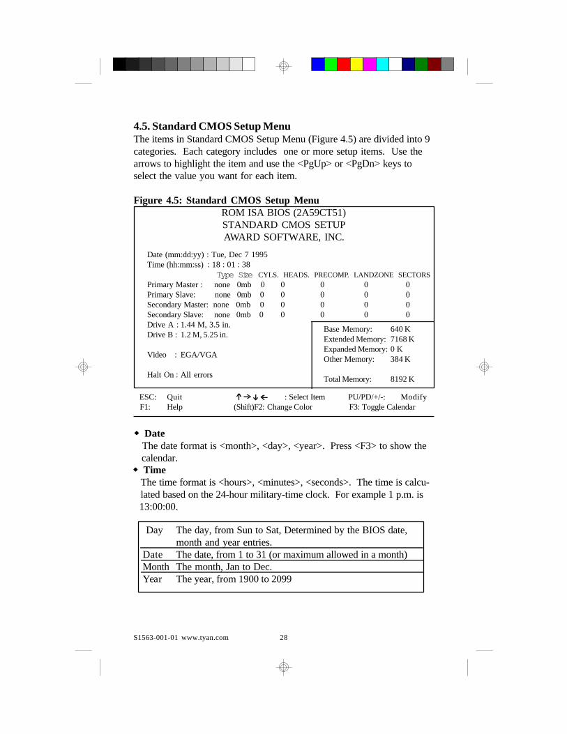
ww Date The date format is <month>, <day>, <year>. Press <F3> to show the calendar.
Base Memory: 640 KExtended Memory: 7168 KExpanded Memory: 0 KOther Memory: 384 K
Total Memory: 8192 K
ESC: Quit : Select Item PU/PD/+/-: Modify F1: Help (Shift)F2: Change Color F3: Toggle Calendar
ww Time The time format is <hours>, <minutes>, <seconds>. The time is calcu- lated based on the 24-hour military-time clock. For example 1 p.m. is 13:00:00.
Date (mm:dd:yy) : Tue, Dec 7 1995Time (hh:mm:ss) : 18 : 01 : 38
Type Size CYLS. HEADS. PRECOMP. LANDZONE SECTORSPrimary Master : none 0mb 0 0 0 0 0Primary Slave: none 0mb 0 0 0 0 0Secondary Master: none 0mb 0 0 0 0 0Secondary Slave: none 0mb 0 0 0 0 0Drive A : 1.44 M, 3.5 in.Drive B : 1.2 M, 5.25 in.
Video : EGA/VGA
Halt On : All errors
4.5. Standard CMOS Setup MenuThe items in Standard CMOS Setup Menu (Figure 4.5) are divided into 9categories. Each category includes one or more setup items. Use thearrows to highlight the item and use the <PgUp> or <PgDn> keys toselect the value you want for each item.
Figure 4.5: Standard CMOS Setup MenuROM ISA BIOS (2A59CT51)STANDARD CMOS SETUPAWARD SOFTWARE, INC.
Day The day, from Sun to Sat, Determined by the BIOS date,month and year entries.
Date The date, from 1 to 31 (or maximum allowed in a month)Month The month, Jan to Dec.Year The year, from 1900 to 2099

29S1563-001-01 www.tyan.com
ww Primary/Secondary Drive type This category identifies the types of hard disk drives that have been in-stalled in the computer. There are 46 predefined types and a user definabletype.
Press PgUp or PgDn to select a numbered hard disk type or type a numberand press <Enter>. Note that the specifications of your drive must matchwith the drive table. The hard disk will not work properly if you enterimproper information for this category. If your hard disk type is not listed,you can Type User to define your own drive manually.
If you select Type User, you will be asked to enter the following info. Enterthe parameters directly from the keyboard and press <Enter>. The harddisk information should be provided in the documentation from the hard diskvendor or the system manufacturer.
CYLS number of cylinders HEADS number of heads PRECOMP written precom LANDZONE landing zone SECTORS number of sectors Mode Normal Access mode for IDE drives under 528MB Mode LBA Access mode for EIDE drives over 528MB Mode Large Access mode for IDE drives over 528MB that don't
support LBA
If a SCSI hard disk has been installed or you have a CD-ROM/Tapedrive connected to an IDE channel, select NONE and press<Enter>.
ww Drive A type/Drive B type This category identifies the types of floppy disk drive A or B, thathave been installed in your computer.
None No floppy drive installed
360K, 5.25 in. 5-1/4 inch PC-type standard drive; 360 kilobyte capacity
1.2M,5.25 in. 5-1/4 inch AT-type high-density drive; 1.2 megabyte capacity
720K, 3.5 in. 3-1/2 inch double-sided drive; 720 kilobyte capacity
1.44M, 3.5 in. 3-1/2 inch double-sided drive; 1.44 megabyte capacity
2.88M, 3.5 in. 3-1/2 inch double-sided drive; 2.88 megabyte capacity

30S1563-001-01 www.tyan.com
ww Video This category detects the type of graphics adapter used for the primarydisplay system. It must match your video display card and monitor. Al-though secondary monitors are supported, you do not have to select thattype in setup.
EGA/VGA Enhanced Graphics Adapter/Video Graphics Array.For VGA,SVGA, or PGA monitor adapters.
CGA 40 Color Graphics Adapter, power up in 40 column mode. CGA 80 Color Graphics Adapter, power up in 80 column mode. Mono Monochrome adapter, includes hi-res monochrome.
ww Halt On The category determines whether the computer will stop if an error is detected during power up.
All errors Whenever the BIOS has detected a non-fatal error, the system will be stopped and you will be promted.
No errors The system boot will not be stopped for any errors that are detected.
All, but Keyboard The system boot will not stop for a keyboard error;it will stop for all other errors.
All, but Diskette The system boot will not stop for disk errors; it will stop for all other errors.
All, but Disk/Key The system boot will not stop for a keyboard or disk error; it will stop for all other errors.
ww Memory The category is for display-only and it is determined by POST Power On Self Test of the BIOS.
Base MemoryThe POST of the BIOS will determine the amount ofbase (or conventional) memory installed in the system.The value of the base memory is typically 640K.
Extended MemoryThe BIOS determines how much extended memory ispresent during the POST. This is the amount ofmemory located above 1MB in the CPU's memoryaddress map.
31S1563-001-01 www.tyan.com
Expanded MemoryExpanded Memory (EMS) defines a 64 K page frame inthe area between 640K and 1Mb containing four 16K pagesthat are windows into the EMS memory. Programs issuerequests to the EMS manager to switch the page to anypart of EMS memory. Extended memory can be convertedto emulate EMS by using a memory manager such asEMM386 that ships with Windows and DOS.
Other MemoryThis refers to memory located in the 640K to 1024K address space. This memory can be used for differentapplications. DOS uses this area to load device drivers tokeep as much conventional memory free for applicationprograms as possible.
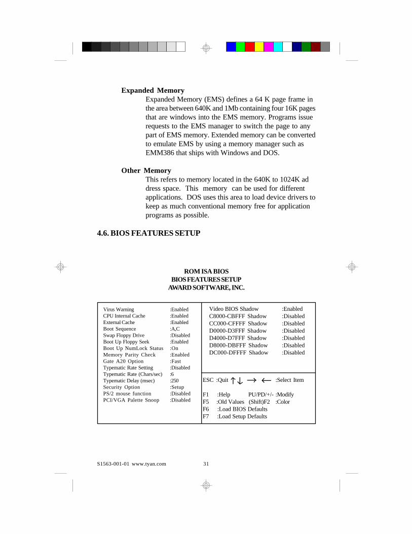
4.6. BIOS FEATURES SETUP
ROM ISA BIOSBIOS FEATURES SETUP
AWARD SOFTWARE, INC.
Video BIOS Shadow :EnabledC8000-CBFFF Shadow :DisabledCC000-CFFFF Shadow :DisabledD0000-D3FFF Shadow :DisabledD4000-D7FFF Shadow :DisabledD8000-DBFFF Shadow :DisabledDC000-DFFFF Shadow :Disabled
Virus Warning :EnabledCPU Internal Cache :EnabledExternal Cache :EnabledBoot Sequence :A,CSwap Floppy Drive :DisabledBoot Up Floppy Seek :EnabledBoot Up NumLock Status :OnMemory Parity Check :EnabledGate A20 Option :FastTypematic Rate Setting :DisabledTypematic Rate (Chars/sec) :6Typematic Delay (msec) :250Security Option :SetupPS/2 mouse function :DisabledPCI/VGA Palette Snoop :Disabled
ESC :Quit :Select Item
F1 :Help PU/PD/+/- :ModifyF5 :Old Values (Shift)F2 :ColorF6 :Load BIOS DefaultsF7 :Load Setup Defaults

32S1563-001-01 www.tyan.com
ww Virus warning This category flashes on screen. During and after the system boot up, any attempt to write to the boot sector or the partition table of the hard disk drive will halt the system and the following error message will appear. In the meantime, you can run an anti-virus program to locate the problem. Default value is Enabled.
Enabled Activate automatically when the system boots up causing a warningmessage to appear when anything attemps to access the boot sectoror hard disk partition table.
Disable No warning message to appear when anything attemps to access theboot sector or hard disk partition table.
ww CPU Internal Cache/External Cache These two categories speed up the memory access. However, it de- pends on the CPU/Chipset design. Default value is Enabled.
Enabled Enables the cache
Disabled Disables the cache
ww Boot Sequence This category determines which drive the computer searches first for the disk operating system (i.e. DOS). Default value is A,C.
A,C System will first search for floppy disk drive then hard disk drive.
C,A System will first search for hard disk drive then floppy disk drive
ww Swap Floppy Drive Default value is Disabled
Enabled Floppy A & B will be swapped under DOS
Disable Floppy A & B will be normal definition.

33S1563-001-01 www.tyan.com
ww Boot Up Floppy Seek During POST, the BIOS will determine if the floppy disk drive installed is 40 or 80 tracks. 360K type is 40 tracks while 720K, 1.2M and 1.44M are all 80 tracks. Default value is Enabled
Enabled BIOS searches for floppy disk drive to determined if it is 40 or 80 tracks. Note that the BIOS cannot tell from 720k, 1.2M or 1.44M drive type as they are all 80 tracks
Disabled BIOS will not search for the type of floppy disk drive by track number. Note that there will not be any warning messages if the drive installed is 360K
ww Boot Up NumLock Status Default value is On
On Keypad is number keys
Off Keypad is arrow keys
ww Memory Parity Check The default value is disabled
ww Gate A20 Option Gate A20 controls the ability to access memory addresses above 1 MB by enabling (Fast) or disabling (Normal) access to the processor. Default value is Fast
ww Typematic Rate Setting, Typematic Rate (char/sec), andTypematic Delay. Typematic Rate Setting enables or disables the following two options.TheTypematic Rate (6, 8, 10, 12, 15, 20, 24, or 30 characters per second)and Typematic Rate Delay (250, 500, 750, or 1000 milliseconds) controlsthe speed at which the keystroke is repeated. The selected character isdisplayed when a key is held down after a delay set by the TypematicRate Delay. It then repeats at a rate set by the Typematic Rate.
34S1563-001-01 www.tyan.com
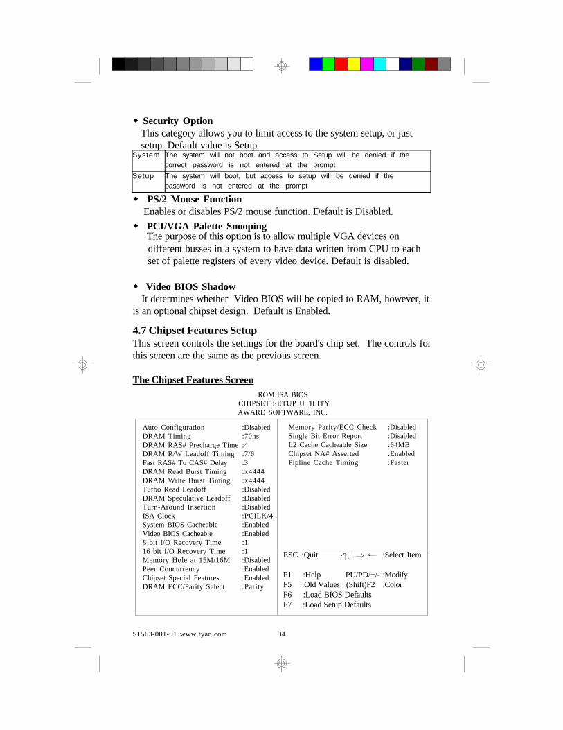
ROM ISA BIOS CHIPSET SETUP UTILITYAWARD SOFTWARE, INC.
Auto Configuration :DisabledDRAM Timing :70nsDRAM RAS# Precharge Time :4DRAM R/W Leadoff Timing :7/6Fast RAS# To CAS# Delay :3DRAM Read Burst Timing :x4444DRAM Write Burst Timing :x4444Turbo Read Leadoff :DisabledDRAM Speculative Leadoff :DisabledTurn-Around Insertion :DisabledISA Clock :PCILK/4System BIOS Cacheable :EnabledVideo BIOS Cacheable :Enabled8 bit I/O Recovery Time :116 bit I/O Recovery Time :1Memory Hole at 15M/16M :DisabledPeer Concurrency :EnabledChipset Special Features :EnabledDRAM ECC/Parity Select :Parity
Memory Parity/ECC Check :DisabledSingle Bit Error Report :DisabledL2 Cache Cacheable Size :64MBChipset NA# Asserted :EnabledPipline Cache Timing :Faster
4.7 Chipset Features SetupThis screen controls the settings for the board's chip set. The controls forthis screen are the same as the previous screen.
The Chipset Features Screen
ESC :Quit :Select Item
F1 :Help PU/PD/+/- :ModifyF5 :Old Values (Shift)F2 :ColorF6 :Load BIOS DefaultsF7 :Load Setup Defaults
ww Security Option This category allows you to limit access to the system setup, or just setup. Default value is SetupSystem The system will not boot and access to Setup will be denied if the
correct password is not entered at the prompt
Setup The system will boot, but access to setup will be denied if thepassword is not entered at the prompt
ww PS/2 Mouse Function Enables or disables PS/2 mouse function. Default is Disabled.
ww PCI/VGA Palette Snooping The purpose of this option is to allow multiple VGA devices on different busses in a system to have data written from CPU to each set of palette registers of every video device. Default is disabled.
ww Video BIOS Shadow It determines whether Video BIOS will be copied to RAM, however, itis an optional chipset design. Default is Enabled.
35S1563-001-01 www.tyan.com
ww Chipset Features The DRAM timings can be altered from the default to optimize system performance. Be aware though that these settings are sensitive to the type and speed of DRAMs being used and can cause lockups or data lost if set incorrectly. The default settings should work with most DRAMs.
w DRAM RAS# Precharge Time DRAM must continually be refreshed or it will lose its data. Normally, DRAM is refreshed entirely as the result of a single request. This option allows you to determine the number of CPU clocks allocated for the Row Address Strobe to accumulate its charge before the DRAM is refreshed. If insufficient time is allowed, refresh may be incomplete and data will be lost. A lower setting may increase performance. The default value is 4 clocks.
wwDRAM R/W Leadoff Timing This sets the number of CPU clocks allowed before reads and writes to DRAM are performed. The default of 8/7 would set the leadoff timing for reads to eight clocks and writes to seven clocks. A lower setting may increase performance. The default value is 8/7.
ww DRAM RAS to CAS Delay When DRAM is refreshed, both rows and columns are addressed separately. This option allows you to determine the timing of the transition from Row Address Strobe (RAS) to Column Address Strobe(CAS). A lower setting may increase performance. The default is 3 cpu clock delay.
wwDRAM Read/Write Burst Timing This sets the timing for Burst mode reads from DRAM. Burst read and write requests are generated by the CPU in four separate parts. The "x" is the leadoff cycle and is determined by the chipset and the memory timing. The remaining four numbers is the actual data cycles. The lower the timing numbers, the faster the system will address memory. The default for read burst timing is x4444. The default for write burst timing is x4444.
36S1563-001-01 www.tyan.com
wwSpeculative Leadoff The 430HX chipset is capable of allowing a DRAM read request to be generated slightly before the address has been fully decoded. This can reduce all read latencies.
More simply, the CPU will issue a read request and included with this request is the place(address) in memory where the desired data is to be found. This request is received by the DRAM controller. When enabled, the controller will issue the read command slightly before it has finished determining the address. The default is disabled.
wwTurn-Around Insertion When this is enabled, the chipset will insert one extra clock to the turn-around of back to back DRAM cycles. The default is disabled.
ww System BIOS Cacheable When enabled, accesses to the system BIOS ROM addressed at F0000H-FFFFFH are cached. Enable this for best performance under DOS/Windows or Windows95. When using operating systems that do not access the BIOS (Unix, OS/2, NT, etc...) this setting can be disabled. The default is enabled.
wwVideo BIOS Cacheable As with caching the system BIOS above, enabling the Video BIOS cache will cause access to the video BOS addressed at C0000h to C7FFFFh to be cached. The default is enabled.
ww8/16 bit I/O Recovery Time The recovery time is the length of time measured in CPU clocks, which the system will delay after the completion of an I/O request. This delay takes place because the CPU is operationg so much faster than the I/O bus that the CPU must be delayed to allow for the completion of the I/O request. This option allows you to determine the recovery time allowed for 8/16 bit I/O. The default is 1 clock cycle.

37S1563-001-01 www.tyan.com
wwMemory Hole at 15M-16M Some ISA cards may not function correctly when more than 16MB of RAM is installed. If this is the case, then enable this option. Most ISA card should work fine with this option disabled. The default is disabled.
wwIDE HDD Block Mode This option allows the hard disk controller to use fast block mode transfer to and from the hard disk drive. The hard drive must support block mode transfer for this option to be enabled.(Most new drives do.) If you are not sure if your drive supports this, call your hard drive vendor. The default is enabled.
wwIDE 32-bit Transfer Mode Enabling 32-bit transfer mode allows faster access to data on your hard disk drive. Not all drives will support this feature. The default is enabled.
wwIDE Primary/Secondary Master/Slave PIO Rather than have the BIOS issue a series of commands to effect a transfer to or from the disk drive, PIO(Programmed Input/Output) allows the BIOS to tell the controller what it wants and lets the controller and the CPU perform the complete task themselves. This method is simpler, more efficeint and faster. This BIOS supports five modes (0 thru 4) and can be set by the user or set to Auto detect. The default is Auto.
wwOn-Chip Primary/Secondary PCI IDE This option enables or disables the on board PCI IDE controllers. The default is enabled.
wwPCI Slot IDE 2nd Channel This option allows you to designate an IDE controller board inserted into one of the physical PCI slots as a secondary IDE controller. If you don't have a third party PCI IDE controller installed, this option should be disabled. The default is disabled.

38S1563-001-01 www.tyan.com
wwPeer Concurrency When enabled, multiple PCI devices can be active at any one time. When disabled, only one PCI device can have access to the PCI bus. at any one time. The default is Enabled.
wwChipset Special Features When disabled, the chipset behaves as if it were the earlier 430FX chipset. This option should be enabled for best performance. The default is Enabled.
wwDRAM ECC/Parity Select This item allows you to select between two methods of DRAM error checking, ECC or Parity. Must have parity SIMMs to select ECC or Parity. The ECC algorithm is built into the chipset and can correct one bit errors. The default is Parity.

39S1563-001-01 www.tyan.com
4.7.1 Power Management Setup
ROM ISA BIOS POWER MANAGEMENT SETUP
AWARD SOFTWARE, INC
Power Management :Disabled IRQ3 (Com2) :Off PM Control By APM :No IRQ4 (Com1) :Off Video Off Method :Blank Screen IRQ5 (LPT2) :Off
IRQ6 (Floppy Disk) :Off Doze Mode :Disabled IRQ7 (LPT1) :Off Standby Mode :Disabled IRQ8 (RTC Timer) :Off Suspend Mode :Disabled IRQ9 (IRQ2 Redir) :Off HDD Power Down :Disabled IRQ10 (Reserved) :Off
IRQ11 (Reserved) :Off IRQ3 (Wake-Up Event) :Off IRQ12 (PS/2 Mouse) :Off IRQ4 (Wake-Up Event) :Off IRQ13 (Coprocessor) :Off IRQ8 (Wake-Up Event) :Off IRQ14 (Hard Disk) :Off IRQ12 (Wake-Up Event) :Off IRQ15 (Reserved) :Off
wwPower Management Options are disabled, user defined, Min saving, and Max saving.
wwPM Control by APM(Advanced Power Management) Options are "Yes" and "No". When set for "No", system BIOS will ignore APM when power managing the system. If set on "Yes" the system BIOS will wait for APM's prompt before it enters any PM mode, e.g. Doze, Standby or Suspend.
wwVideo Off Method The "Blank Screen" option will let the system BIOS blanks the screen when disabling video. V/H SYNC+Blank will let the BIOS turn off the V-SYNC and H-SYNC signals from the VGA card to the monitor.

40S1563-001-01 www.tyan.com
wwDoze ModeDefines the continous idle time before the system enters Doze mode.
wwStandby ModeDefines the continous idle time before the system enters Standby mode.
wwPower Down ActivitiesDefines the the activities that can cause the PM timers to reload. (Break-ing out of PM Mode)

41S1563-001-01 www.tyan.com
4.8 PCI Slot Configuration
ROM ISA BIOSPCI/PNP Configuration
AWARD SOFTWARE, INC.
Resource Controlled by :Manual PCI IRQ Actived by :LevelReset Configuration :Disabled PCI IDE IRQ Map to :PCI-Auto
Primary IDE INT# :AIRQ3 assigned to :legacy ISA Secondary IDE INT# :BIRQ4 assigned to :legacy ISAIRQ5 assigned to :PCI/PnPIRQ7 assigned to :legacy ISAIRQ9 assigned to :PCI/PnPIRQ10 assigned to :PCI/PnPIRQ11 assigned to :PCI/PnPIRQ12 assigned to :PCI/PnPIRQ14 assigned to :legacy ISAIRQ15 assigned to :legacy ISADMA0 assigned to :PCI/PnPDMA1 assigned to :PCI/PnPDMA3 assigned to :PCI/PnPDMA5 assigned to :PCI/PnPDMA6 assigned to :PCI/PnPDMA7 assigned to :PCI/PnP
w PCI Slot 1/Slot 2/Slot 3/Slot 4/Slot 5 INT# w For Default Setting. Connect to PCI System INT# PCI Slot1 INTA INTA PCI Slot1 INTB INTB PCI Slot1 INTC INTC PCI Slot1 INTD INTD PCI Slot2 INTA INTB PCI Slot2 INTB INTC PCI Slot2 INTC INTD PCI Slot2 INTD INTA PCI Slot3 INTA INTC PCI Slot3 INTB INTD PCI Slot3 INTC INTA PCI Slot3 INTD INTB PCI Slot4 INTA INTD PCI Slot4 INTB INTA PCI Slot4 INTC INTB PCI Slot4 INTD INTC PCI Slot5 INTA INTA PCI Slot5 INTB INTB PCI Slot5 INTC INTC
PCI Slot5 INTD INTD
ESC: Quit :Select ItemF1 : Help PU/PD/+/- :ModifyF5 : Old Values (Shift)F2 :ColorF6 : Load BIOS DefaultsF7 : Load Setup Defaults

42S1563-001-01 www.tyan.com
wwResources Controlled By The Award Plug and Play BIOS can automatically configure all the boot and Plug and Play compatible devices. If you seelect Auto, all the interrupt request and DMA assignment fields disappear, as the BIOS automatically assigns them.
wwIRQ n assigned to When resources are controlled manually, assign each system interrupt as one of the following types, depending on the type of device using the interrupt.
Legacy ISA Devices compliant with the original PC AT bus specification.
PCI/ISA PnP Devices compliant with the Plug and Play standard, whether designed for the PCI or ISA bus architecture.
wwPCI IRQ Activated By: Select the PCI IRQ Active scheme either LEVEL or EDGE. Default value is LEVEL.
wwPCI IDE IRQ Map To: Select the IDE IRQ Map to ISA IRQ#.
wwPrimary IDE INT# Select the PCI INT# that the Primary IDE controller will use. Default value is A.
wwSecondary IDE INT# Select the PCI INT# that the Secondary IDE controller will use. Default value is B
43S1563-001-01 www.tyan.com
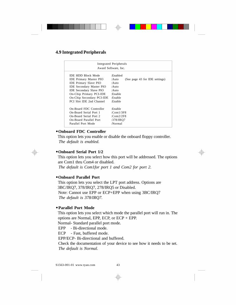
4.9 Integrated Peripherals
Integrated Peripherals
Award Software, Inc.
IDE HDD Block Mode :EnabledIDE Primary Master PIO :Auto (See page 43 for IDE settings)IDE Primary Slave PIO :AutoIDE Secondary Master PIO :AutoIDE Secondary Slave PIO :AutoOn-Chip Primary PCI-IDE :EnableOn-Chip Secondary PCI-IDE :EnablePCI Slot IDE 2nd Channel :Enable
On-Board FDC Controller :EnableOn-Board Serial Port 1 :Com1/3F8On-Board Serial Port 2 :Com2/2F8On-Board Parallel Port :378/IRQ7Parallel Port Mode :Normal
wwOnboard FDC Controller This option lets you enable or disable the onboard floppy controller. The default is enabled.
wwOnboard Serial Port 1/2 This option lets you select how this port will be addressed. The options are Com1 thru Com4 or disabled. The default is Com1for port 1 and Com2 for port 2.
wwOnboard Parallel Port This option lets you select the LPT port address. Options are 3BC/IRQ7, 378/IRQ7, 278/IRQ5 or Disabled. Note: Cannot use EPP or ECP+EPP when using 3BC/IRQ7 The default is 378/IRQ7.
wwParallel Port Mode This option lets you select which mode the parallel port will run in. The options are Normal, EPP, ECP, or ECP + EPP. Normal- Standard parallel port mode. EPP - Bi-directional mode. ECP - Fast, buffered mode. EPP/ECP- Bi-directional and buffered. Check the documentation of your device to see how it needs to be set. The default is Normal.

44S1563-001-01 www.tyan.com
STANDARD CMOS SETUP PASSWORD SETTING
BIOS FEATURES SETUP IDE HDD AUTO DETECTION
CHIPSET FEATURES SETUP DAVE & EXIT SETUP
PCI SLOT configuration EXIT WITH OUT SAVING
LOAD SETUP DEFAULTS
4.10. LOAD SETUP DEFAULTS
ROM ISA BIOSCMOS SETUP UTILITY
AWARD SOFTWARE INC.
ESC : Save & Exit Setup F10 : Quit (Shift)F2 :Change Color
:Select Item
Load SETUP Defaults except standard CMOS SETUP
ww Load SETUP defaults To load SETUP default values to CMOS SRAM, enter "Y". If not, enter "N"
ww If any problem has occurred, loading the SETUP DEFAULTSisrecommended.
4.11. PASSWORD SETTING
When you select this function, the following message will appear at thecenter of the screen to assist you in creating a password.
ENTER PASSWORD
Load Setup Defaults (Y/N)? N

45S1563-001-01 www.tyan.com
ROM ISA BIOSCMOS SETUP UTILITY
AWARD SOFTWARE, INC.
STANDARD CMOS SETUP PASSWORD SETTING
BIOS FEATURES SETUP IDE HDD AUTO DETECTION
CHIPSET FEATURES SETUP DAVE & EXIT SETUP
PCI SLOT CONFIGURATION EXIT WITH OUT SAVING
LOAD SETUP DEFAULTS
ESC : Save & Exit Setup F10 : Quit (Shift)F2 :Change Color
:Select Item
Change/Set/Disable Password
Type the password, up to eight characters, and press <Enter>. Thepassword typed now will clear the previously entered password fromCMOS memory. You will be asked to confirm the password. Type thepassword again and press <Enter>. You may also just press <Esc> toabort the selection and not enter a password.
To disable the password, just press <Enter> when you are prompted toenter a password. A message will confirm that the password has beendisabled, the system will boot and you can enter Setup freely.
PASSWORD DISABLED
If you select System at Security Option of BIOS Features Setup Menu, youwill be prompted for the password every time the system is rebooted or anytime you try to enter setup. If you select Setup at Security Option of BIOSFeatures Setup Menu, you will be prompted only when you try to entersetup.
Enter Password
46S1563-001-01 www.tyan.com
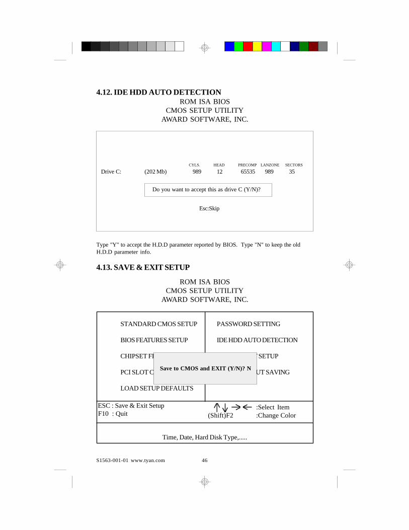
4.12. IDE HDD AUTO DETECTIONROM ISA BIOS
CMOS SETUP UTILITYAWARD SOFTWARE, INC.
CYLS. HEAD PRECOMP LANZONE SECTORS
Drive C: (202 Mb) 989 12 65535 989 35
Do you want to accept this as drive C (Y/N)?
Esc:Skip
Type "Y" to accept the H.D.D parameter reported by BIOS. Type "N" to keep the oldH.D.D parameter info.
4.13. SAVE & EXIT SETUP
STANDARD CMOS SETUP PASSWORD SETTING
BIOS FEATURES SETUP IDE HDD AUTO DETECTION
CHIPSET FEATURES SETUP DAVE & EXIT SETUP
PCI SLOT CONFIGURATION EXIT WITH OUT SAVING
LOAD SETUP DEFAULTS
ESC : Save & Exit Setup F10 : Quit (Shift)F2 :Change Color
:Select Item
Time, Date, Hard Disk Type,.....
ROM ISA BIOSCMOS SETUP UTILITY
AWARD SOFTWARE, INC.
Save to CMOS and EXIT (Y/N)? N
47S1563-001-01 www.tyan.com
Type "Y" and you will quit the Setup Utility and save the user setup valuesto RTC CMOS SRAM. Type "N" to return to Setup Utility.
4.14 KEYBOARD SETTING FUNCTION
After booting the O.S., there are some special functions used by the key-board as follows:"CTRL_ALT_DEL" -Pressing these keys simultaneously will cause the
system to WARM START/BOOT(Soft Reset).

48S1563-001-01 www.tyan.com
5.0 AMI WINBIOS
The AMI WINBIOS is based on a Graphical User Interface that enablesthe user to access all of the BIOS setup options with either a mouse orkeyboard. You can enter the BIOS setup by pressing the "DEL" key duringthe memory test/count.The WINBIOS Setup screen consists of the following option groups:
American AMIBIOS Setup
Megatrends (C)1995, American Megatrends Inc.
Setup Security
Standard Advanced Chipset Supervisor User
Power Mgnt PCI/Pnp Peripheral Anti-Virus
Utility Default
Color Set Language Original Optimal Fail-safe
Alt+H: Help
5.1 Standard Setup Options
Date, Day and Time ConfigurationSelect the Standard Option, then select the Date and Time Icon. The cur-rent values for each category are displayed. Use the arrow keys or mouseto highlight the date or time fields. Use the + or - keys the change the fieldvalues. The system will automatically select the appropriate day of the week.

49S1563-001-01 www.tyan.com
wwPrimary/Secondary MasterwwPrimary/Secondary SlaveSelect one of these hard disk drive icons to configure the drive named in theoption. WINBIOS supports up to four IDE hard disk drives: the primarymaster, primary slave, secondary master and secondary slave. If the harddisk drive is an IDE drive, select DETECT PRIMARY or DETECT SLAVEfrom the Utility Setup Option Section of the WINBIOS Setup Main Menuto have WINBIOS automatically detect the IDE drive parameters and re-port them to this screen.The SCSI option or none must be selected if aSCSI Disk Drive is installed.For CD-ROM drives you should use none.
You can also manually enter the hard disk drive parameters. Hard disk type47 is the user-definable drive type. The drive parameters are: Type, Cylin-ders, Heads, Write precompensation, Landing Zone, Sectors and Capacity.
ww Floppy Drive A:ww Floppy Drive B:Move the cursor to these fields via the up and down arrow keys and selectthe floppy type. The settings are 360 KB 5 1/4 inch, 1.2MB 5 1/4 inch,720MB 3 1/2 inch, 1.44MB 3 1/2 inch and 2.88MB 3 1/2 inch..
5.2 Advanced Setup
The WINBIOS Setup options described in this section are selected bychoosing the Advanced Setup Icon from the WINBIOS Setup MainMenu.
ww Quick Boot When enabled the BIOS will skip the memory test and will not access the floppy drive during POST. When enabled the BIOS does a memory test and will access and verify floppy drive types. The default is Enabled.
wwBootUp Sequence This option let the user specify in what sequence the BIOS will look for a boot device. Options are A:C:, CDROM, C:A:,CDROM or CDROM,C:A:. The default is C:A:,CDROM.

50S1563-001-01 www.tyan.com
wwBootUp Num-Lock This option gives the user the option to turn on or off the num-lock on boot-up. The default is On.
wwFloppy Drive Swap When enabled, the system allows the floppy drives to swap drive letters with each other. The default is disabled.
wwMouse Support Enable or disable the onboard PS/2 support.. The default is enabled.
wwPrimary Display This option detects the primary graphics display system. The default is VGA/EGA.
wwPassword Check This option enables the password check option everytime the system boots or the user runs WinBIOS setup. If Always is chosen, a user password prompt appears everytime the computer is powered on. If Setup is chosen, the passwrd prompt appears if WinBIOS setup is executed. The default is Setup.
wwOS/2 Compatible Mode This option lets you turn on or off the BIOS support for OS/2. The default is disabled.
wwInternal Cache This option lets the user enable or disable the Pentiums level 1 cache. When this option is set for WriteBack the CPUs level 1 cache is enabled. When this option is set for Disabled, the CPU will not use its internal cache. The default is WriteBack.
wwExternal Cache This option lets the user enable or disable the mainboards level 2 cache. The default is Enabled.

51S1563-001-01 www.tyan.com
wwSystem BIOS Cacheable If this option is enabled, the F000 segment of the BIOS shadow will be cached. The default is enabled.
ww Adaptor ROM Shadow C000 to DC00 The adaptor ROMs present on the system may either execute out of ROM(disabled), RAM(Shadow), or execute out of RAM and be cached(Cache). The adaptor ROM area should be left disabled unless the device in that region can support shadowing (Its ROM being copied to RAM for better performance). The default is disabled.

52S1563-001-01 www.tyan.com
5.3 Advanced Chipset
wwGlobal 430HX Enable This option provides a method to enable or disable all of the additional features provided by the 430HX chipset(enhancements to 430FX).
wwShutdown to Port 92 When disabled, the 430HX forwards a Shutdown special cycle from the host bus to the PCI bus. When enabled, the TXC will write a 1 to I/O address 92 in response to a shutdown special cycle on the host bus. The default is disabled.
wwMemory Hole This option lets you create a memory hole for either the 512-640KB region or the 15-16MB region. The default is disabled.
ww IRQ12/M Mouse Function Enables or disables PS/2 mouse access to IRQ12. The default is enabled.
ww8 bit I/O Recovery Time 16 bit I/O Recovery Time These options set the 8 bit and 16 bit I/O recovery time in the chipset. I/O devices may not function correctly if two back to back I/O writes occur too close together. These options increase the delay between back to back I/O instructions. The options for 8 bit are 1,2,3,4,5,6,7,8 Sysclk or Disabled. The options for 16 bit are 1,2,3,4 Sysclk or Disabled. The default for both options is 1 Sysclk.
wwDRAM Timing This setup question allows the system to be set to either optimal settings for 60ns or 70ns DRAM, or to be set to manual. In this mode the next nine options are made available for customizing the memory timing.

53S1563-001-01 www.tyan.com
♦Refresh Rate Allows the refresh rate to be set according to the memory bus clock (50mhz, 60mhz or 66mhz). The default depends on CPU speed.
♦Turbo Read LeadOff A feature to enable the skipping of the first input register in the DRAM data pipeline. This results in a 1 HCLK savings of all READ leadoff timings.
♦Read/Write Burst Timing Allows customizing of the read timings in the memory design. The options are x2222, x3333 and x4444. The lower the number, the faster the DRAM will be accessed.
♦Fast RAS to CAS Delay (Clocks) If enabled, the row miss leadoff timing delay is set to 2 clocks, other wise it is set to 3 clocks. The default is 7/6/3/4.
♦LeadOff Timing This bit controls additional DRAM timings. This includes: Read LeadOff, Write LeadOff, RAS# Precharge, and Refresh RAS asser- tion.
♦Turbo Read Pipelining This bit affects the Read timings. The options are enabled or disabled. The default is disabled.
♦Speculative LeadOff In this mode the DRAM controller read request is presented before the final memory target (main memory, cache, or PCI) is decoded. This results in a 1 HCLK increase in DRAM read leadoff latencies. The default is disabled.
♦Turn-Around Insertion When enabled the chipset inserts 1 extra clock of turnaround on the MD lines after asserting memory write enable (MWE#).

54S1563-001-01 www.tyan.com
♦Memory Address Drive Strength This setup option allows the selection of memory address output buffer drive affecting the MA(memory address) and MWE#(memory write enale)pins. The default is 8ma/8ma.
♦NA Disable (NAD) For External Cache When enabled the NA#(next address) pin is never asserted, otherwise the assertion is dependent upon the cache type and size. The default is enabled.
♦Peer Concurrency When enabled the CPU will be allowed to run DRAM/L2 cycles when non-PHLD( PCI masters are running non-locked cycles targeting PCI peer devices. The default is enabled.
♦ECC Test This is a test mode described in the 430HX( Xcellerated Controller) external design specification. This should be enabled only when using ECC memory. The default is disabled.
♦DRAM Data Integrity Mode This option allows the selection of the DRAM error detection. Either parity or ECC modes are supported. The default is parity.
♦SERR# (System Error)Output Type This allows the selection of the output type of the SERR# signal. Valid options are Open drain and Normal (actively driven high). The default is normal.
♦SERR#(System Error) Duration Mode This option allows the determination of the SERR# output’s duration when it is asserted. The modes are Pulse (asserted for 1PCLK), or Level (asserted until the error flags are cleared). The default is Pulse.
♦SERR# (System Error)Enable This is the master enable bit for SERR# generation. The default is disabled.

55S1563-001-01 www.tyan.com
♦SingleBit Correctable Error This option if enabled will assert SERR# upon the detection of a single bit error (SBE). The default is disabled.
♦MultiBit Uncorrectable Error This option if enabled will assert SERR# upon the detection of a multi bit error (MBE) or parity error. The default is disabled.
♦Bad Parity On Uncorrectable Error The TXC forces bad parity on PCI read data starting from the time an uncorrectable DRAM error is detected,until the end of the current cycle. The default is disabled.
♦PCI 2.1 Passive Release Enable If enabled, this option causes the PIIX3 to use the passive release mechanism on the PHOLD# signal. If disabled the PHOLD# signal behaves as it did previously with the Triton I chipset. The default is enabled.
♦Delayed Transaction Enable If enabled the delayed transaction mechanism is used when the PIIX3 is the target of a PCI transaction. The default is enabled.

56S1563-001-01 www.tyan.com
5.4 Power Management
wwAdvanced Power Management This option enables or disables power management. The default is disabled.
wwStandby to Suspend Timeout Value This option indicates the time before standby and suspend power saving modes will occur. The options are from disabled thru 255 minutes. The default is disabled.
wwIDE Drive Power Down In This option specifies which mode the IDE drives will power down in. The options are disabled, standby or suspend. The default is disabled.
wwVESA Video Power Down In This option specifies which mode the video will power down in. The options are disabled, standby or suspend. The default is disabled.
wwVESA Power Down In This option specifies the power saving mode for the video. The options are standy, suspend or off. The default is standby.
wwSlow Clock Ratio This ratio indicates the amount the CPU will be slowed when the CPU enters standby mode. The default is 1:1.
wwIRQ x Break Event (x= 0 to 15) These break events indicate which IRQ events will wake up the system and/or reload the standby and suspend timers. The options are disabled and enabled. The default is disabled.

57S1563-001-01 www.tyan.com
5.5 Peripheral
wwProgramming Mode When set to manual, you can customize all the settings below. When set to auto, they system will automatically configure all the ports. The default is Manual.
wwOnBoard FDC This option lets you enable or disable the onboard floppy disk controller. The default is enabled.
wwSerial Port 1 This option lets you configure the address of serial port 1. The options are 3F8h, 3E8h, 2E8h or disabled. The default is 3F8h.
wwSerial Port 2 This option lets you configure the address of serial port 2. The options are 2F8h, 3E8h, 2E8h and disabled. The default is 2F8h.
wwParallel Port This option lets you configure the address of the onboard parallel port. The options are 3BCh, 378h, 278h or disabled. The default is 378h.
wwParallel Port Mode This option lets you configure the mode that the onboard parallel port will function in. The options are Extended or Normal. The default is Extended.
wwIRQ Active This options lets you set the IRQ trigger. The options are High or Low. The default should be used in most cases. The default is High.

58S1563-001-01 www.tyan.com
5.6 Utility
Detect Master/Detect SlaveThese options, when invoked will enable the CMOS to query the IDEdrive firmware for its cylinder, head and sector parameters.
Color SetThis option lets you select the color scheme of the WinBIOS setupscreen. The options are LCD, Army, Pastel and Sky.The default is LCD (Very boring).
5.7 Security
PasswordThe password feature prohibits unauthorized changes to the system setupaccessed via the CMOS setup program. The default password is "AMI".
Anti-VirusIf enabled, this option will protect the boot sector of the hard disk drive.Nothing can be written to the boot sector while this option is enabled.This option should be disabled if you are installing a new operating systemthat writes to the boot sector. The default is disabled.
5.8 Defaults
OriginalThis option restores the CMOS setup to factory default settings.
OptimalThis option will configure the CMOS setup to its fastest settings.
Fail-SafeThis option will configure the CMOS setup to its most conservativesettings.
CMOS Save & ExitTo save the changes made to the CMOS setup, press the ESCape keyunitl the "exit CMOS" menu appears, then select your choice.

59S1563-001-01 www.tyan.com
6.0 Flash Writer Utility
You can upgrade the BIOS of your mainboard by using a "FlashMemory Writer"(FMW) utility. This utility can be downloaded from thefactory's BBS(Consult your system vendor for the phone #). Thesystem BIOS is stored on a 'flash' EPROM chip on the mainboardwhich can be erased and reprogrammed by the FMW.The following three files make up the FMW.
AWDFLASH.EXE -The Flash Memory Writer utility for Award to Award upgrade.
AMIFLASH.COM -The Flash Memory Writer utility for AMI to AMI upgrade.
README -A text file of instructions*S56AWXX.BIN -XX-A 2-digit version number.
Flash memory writer records (or ‘programs’) a new BIOSonto the flash memory chip. You cannot upgrade an AwardBIOS to a AMI BIOS or a AMI BIOS to an Award BIOS.
*This file name is subject to change and can have either a "bin" or a"rom" extension.

60S1563-001-01 www.tyan.com
To reprogram the System BIOS, you must first do the following:
1. Check jumpers J48
The S1563 uses a 5V Flash EPROM so jumper J48should be left in the default postion on pins 1 and 2. Thisjumpers should never be moved.
2. Make sure the CPU is running in ‘real mode’.
FMW will not run if the CPU is operating in a protected orvirtual mode. This means that you can not run it with Windowsrunning or with any memory manager software. You mustdisable any memory manager first. The easiest way to do thisis to:
a. Boot your system from a bootable floppy disk with noCONFIG.SYS or AUTOEXEC.BAT files, and then run FlashMemory Writer from a backup copy of your support disk. Youcan make your back-up floppy bootable when you format it, anduse one disk for both purposes.
b. If you are using MS-DOS 6.x, you can use the feature thatallows you to bypass the CONFIG.SYS and AUTOEXEC.BAT
file. You do this while pressing <F5> while the “Starting MS-DOS...” line is on the screen.
There are other ways to accomplish the same result. The mainpoint is to make sure no memory managers are running. If youare not sure, try running FMW. If it runs, then you have suc-ceeded. If it displays a warning message about the CPUmode, you will have to try again.

61S1563-001-01 www.tyan.com
Once you have satisfied the two requirements mentioned above,you can run FMW. You can copy the contents of the “Flash”directory to your hard drive, or you can run the utility from abackup of the support floppy disk. Make sure the new BIOS fileis in the same directory as the FMW utility.
To run FMW, change to the “Flash” directory if you are not al-ready in it. Type “Awdflash” at the DOS command line and pressthe <Enter> key. The following screen will appear.
6.1 The Flash Memory Writer Utility Screen (Award)
Type in the whole file name, e.g. S56AW10.BIN and confirmthat you want to program the BIOS. The utility will then ‘Blank’,‘Erase’, and then ‘Program’ the flash memory on the mainboard with thenew BIOS file. You should choose “yes” to save the original systemBIOS to a floppy diskette before you program the new BIOS. Thisleaves you with a backup of your original BIOS in case you need to re-install it. This option is highly recommended. If you can not sucessfullyprogram the BIOS file for whatever reason, re-install you original BIOSfrom the backup file.
Warning: If you do not successfully install a complete BIOS filein the flash memory on the Mainboard, your system may not be able toboot. If this happens, it will require service by your system vendor.Follow the requirements and instructions in this section precisely to aviodinconvenience.
FLASH MEMORY WRITER V3.0Copyright (C) 1993, AWARD Software Inc.,
For FX/HX-2A59CT51 Date:4/13/95
File Name to Program:
Error Message:
62S1563-001-01 www.tyan.com
7.0 TIMER & DMA CHANNEL MAP
TIMER MAP: TIMER Channel-0 system timer interruptTIMER Channel-1 DRAM REFRESH requestTIMER Channel-2 SPEAKER tone generator
DMA CHANNELS: DMA Channel-0 AvailableDMA Channel-1 AvailableDMA Channel-2 FLOPPY DISK adapterDMA Channel-3 AvailableDMA Channel-4 Cascade for DMA controller 1DMA Channel-5 AvailableDMA Channel-6 AvailableDMA Channel-7 Available
7.1 INTERRUPT MAP
NMI: Parity check error
IRQ (H/W) 0 System TIMER interrupt from TIMER-01 KEYBOARD output buffer full2 Cascade for IRQ 9-153 SERIAL port 24 SERIAL port 15 PARALLEL port 26 FLOPPY DISK adapter7 PARALLEL port 18 RTC clock9 Available10 Available11 Available12 Available13 MATH co-processor14 HARD DISK controller15 HARD DISK controller