single-supply, rail-to-rail output, cmos amplifier with rail-to-rail output swing optimized for ......
TRANSCRIPT

® INA156
©1999 Burr-Brown Corporation PDS-1565A Printed in U.S.A. December, 1999
FEATURES RAIL-TO-RAIL OUTPUT SWING: Within 20mV
LOW OFFSET DRIFT: ±5µV/°C INTERNAL FIXED GAIN = 10V/V OR 50V/V
SPECIFIED TEMPERATURE RANGE:–55°C to +125°C
LOW INPUT BIAS CURRENT: 1pA
WIDE BANDWIDTH: 550kHz in G = 10
HIGH SLEW RATE: 6.5V/ µs
LOW COST
TINY MSOP-8 PACKAGES
Single-Supply, Rail-to-Rail Output, CMOSINSTRUMENTATION AMPLIFIER
DESCRIPTIONThe INA156 is a low-cost CMOS instrumentationamplifier with rail-to-rail output swing optimized forlow-voltage, single-supply operation.
Wide bandwidth (550kHz in G = 10) and high slewrate (6.5V/µs) make the INA156 suitable for drivingsampling A/D converters as well as general purposeand audio applications. Fast settling time allows usewith higher speed sensors and transducers, and rapidscanning data acquisition systems.
APPLICATIONS INDUSTRIAL SENSOR AMPLIFIERS:
Bridge, RTD, Thermocouple, Flow, Position
MEDICAL EQUIPMENT:
ECG, EEG, EMG Amplifiers
DRIVING A/D CONVERTERS
PCMCIA CARDS
AUDIO PROCESSING
COMMUNICATIONS
TEST EQUIPMENT
LOW COST AUTOMOTIVE INSTRUMENTATION
International Airport Industrial Park • Mailing Address: PO Box 11400, Tucson, AZ 85734 • Street Address: 6730 S. Tucson Bl vd., Tucson, AZ 85706 • Tel: (520) 746-1111Twx: 910-952-1111 • Internet: http://www.burr-brown.com/ • Cable: BBRCORP • Telex: 066-6491 • FAX: (520) 889-1510 • I mmediate Product Info: (800) 548-6132
For most current data sheet and other productinformation, visit www.burr-brown.com
Gain can be set to 10V/V or 50V/V by pin strapping.Gains between these two values can be obtained withthe addition of a single resistor. The INA156 is fullyspecified over the supply range of +2.7V to +5.5V.
The INA156 is available in an MSOP-8 surface-mountpackage specified for operation over the temperaturerange –55°C to 125°C.
22.2kΩ 200kΩ
VIN–
VIN+
Ref
RG
INA156
VO
22.2kΩ
5kΩ5kΩ
200kΩ
RGV+
V–
1
5
2
3
8 7
4
6
A1
A2
G = 10 pins openG = 50 pins connected
VO = (VIN – VIN) • G + VREF+ –
INA156
SBOS119

2®
INA156
SPECIFICATIONS: VS = +2.7V to +5.5VBoldface limits apply over the specified temperature range, TA = –55°C to +125°CAt TA = +25°C, RL = 10kΩ connected to VS/2. RG pins open (G = 10), and Ref = VS /2, unless otherwise noted.
INA156E, A
PARAMETER CONDITION MIN TYP MAX UNITS
INPUTOffset Voltage, RTI VOS VS = +5.0V, VCM = VS/2 ±2.5 ±8 mV
Over Temperature ±9 mVDrift dVOS/dT ±5 µV/°Cvs Power Supply PSRR VS = +2.7V to +6V, VCM = 0.2 • VS ±50 ±200 µV/V
Over Temperature ±250 µV/Vvs Time ±0.4 µV/mo
INPUT VOLTAGE RANGE
Safe Input Voltage (V–) – 0.5 (V+) + 0.5 VCommon-Mode Range(1) VCM VS = 5.5V 0.3 5.2(2) V
VS = 2.7V 0.2 2.5(2) VCommon-Mode Rejection Ratio CMRR VS = 5.5V, 0.6V < VCM < 3.7V, G = 10 66 78 dB
Over Temperature 65 dBVS = 5.5V, 0.6V < VCM < 3.7V, G = 50 74 87 dB
Over Temperature 73 dB
INPUT IMPEDANCEDifferential 1013 || 3 Ω || pFCommon-Mode 1013 || 3 Ω || pF
INPUT BIAS CURRENTInput Bias Current IB ±1 ±10 pAOffset Current IOS ±1 ±10 pA
NOISE, RTI RS = 0Ω, G = 10 or 50Voltage Noise: f = 0.1Hz to 10Hz 4.5 µV/Vp-pVoltage Noise Density: f = 10Hz 260 nV/√Hzf = 100Hz 99 nV/√Hzf = 1kHz 40 nV/√HzCurrent Noise: f = 1kHz 2 fA/√Hz
GAIN 10 50 V/VGain Equation G = 10 + 400kΩ/(10kΩ + RG) V/VGain Error(3) VS = 5.5V, VO = 0.02V to 5.48V, G = 10 ±0.08 ±0.4 %
vs Temperature ±2 ±10 ppm/°CVS = 5.5V, VO = 0.05V to 5.45V, G = 50 ±0.1 ±0.8 %
vs Temperature ±15 ±30 ppm/°CNonlinearity VS = 5.5V, G = 10 or 50 ±0.005 ±0.015 % of FSR
Over Temperature ±0.015 % of FSR
OUTPUTVoltage Output Swing from Rail G = 10, RL = 10kΩ, GERR < 0.4% 5 20 mV
Over Temperature 20 mVShort-Circuit Current Short-Circuit to Ground ±50 mACapacitance Load (stable operation) See Typical Curve
FREQUENCY RESPONSEBandwidth, –3dB BW G = 10 550 kHz
G = 50 110 kHzSlew Rate SR VS = 5.5V, CL = 100pF 6.5 V/µsSettling Time: 0.1% tS VS = 5.5V, VO = 2V Step, CL = 100pF, G = 10 5 µs
VS = 5.5V, VO = 2V Step, CL = 100pF, G = 50 11 µs0.01% VS = 5.5V, VO = 2V Step, CL = 100pF, G = 10 8 µs
VS = 5.5V, VO = 2V Step, CL = 100pF, G = 50 15 µsOverload Recovery 50% Input Overload 0.2 µsTotal Harmonic Distortion + Noise THD+N See Typical Curve
POWER SUPPLYSpecified Voltage Range +2.7 +5.5 VOperating Voltage Range +2.5 to +6 VQuiescent Current VIN = 0, IO = 0 1.8 2.5 mA
Over Temperature V IN = 0, IO = 0 3.2 mA
TEMPERATURE RANGESpecified Range –55 +125 °COperating Range –65 +150 °CStorage Range –65 +150 °CThermal Resistance θJA
MSOP-8 Surface Mount 150 °C/WSO-8 Surface Mount 150 °C/W
NOTES: (1) For further information, refer to typical performance curves on common-mode input range. (2) Operation beyond (V+) – 1.8V (max) results in reduced common-moderejection. See discussion and Figure 6 in the text of this data sheet. (3) Does not include error and TCR of additional optional gain-setting resistor in series with RG, if used.
3®
INA156
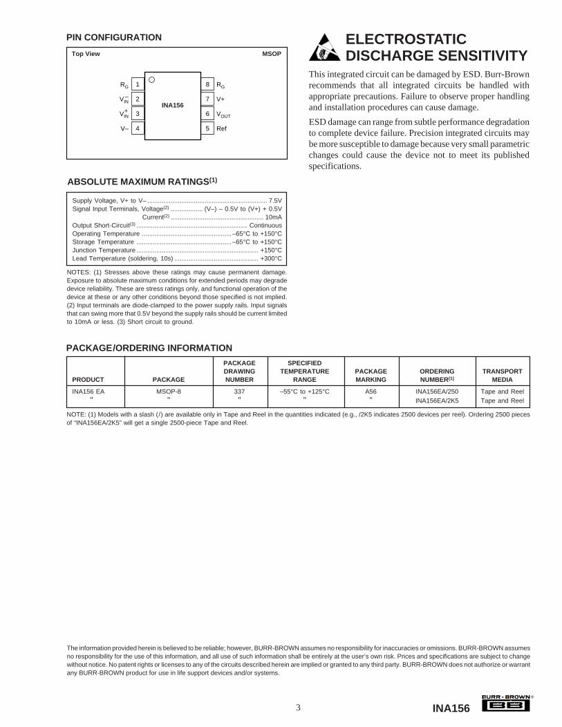
PIN CONFIGURATION ELECTROSTATICDISCHARGE SENSITIVITY
This integrated circuit can be damaged by ESD. Burr-Brownrecommends that all integrated circuits be handled withappropriate precautions. Failure to observe proper handlingand installation procedures can cause damage.
ESD damage can range from subtle performance degradationto complete device failure. Precision integrated circuits maybe more susceptible to damage because very small parametricchanges could cause the device not to meet its publishedspecifications.
The information provided herein is believed to be reliable; however, BURR-BROWN assumes no responsibility for inaccuracies or omissions. BURR-BROWN assumesno responsibility for the use of this information, and all use of such information shall be entirely at the user’s own risk. Prices and specifications are subject to changewithout notice. No patent rights or licenses to any of the circuits described herein are implied or granted to any third party. BURR-BROWN does not authorize or warrantany BURR-BROWN product for use in life support devices and/or systems.
Top View MSOP
Supply Voltage, V+ to V– ................................................................... 7.5VSignal Input Terminals, Voltage(2) .................. (V–) – 0.5V to (V+) + 0.5V
Current(2) .................................................... 10mAOutput Short-Circuit(3) .............................................................. ContinuousOperating Temperature .................................................. –65°C to +150°CStorage Temperature ..................................................... –65°C to +150°CJunction Temperature .................................................................... +150°CLead Temperature (soldering, 10s) ............................................... +300°C
NOTES: (1) Stresses above these ratings may cause permanent damage.Exposure to absolute maximum conditions for extended periods may degradedevice reliability. These are stress ratings only, and functional operation of thedevice at these or any other conditions beyond those specified is not implied.(2) Input terminals are diode-clamped to the power supply rails. Input signalsthat can swing more that 0.5V beyond the supply rails should be current limitedto 10mA or less. (3) Short circuit to ground.
ABSOLUTE MAXIMUM RATINGS (1)
PACKAGE SPECIFIEDDRAWING TEMPERATURE PACKAGE ORDERING TRANSPORT
PRODUCT PACKAGE NUMBER RANGE MARKING NUMBER (1) MEDIA
INA156 EA MSOP-8 337 –55°C to +125°C A56 INA156EA/250 Tape and Reel" " " " " INA156EA/2K5 Tape and Reel
NOTE: (1) Models with a slash (/) are available only in Tape and Reel in the quantities indicated (e.g., /2K5 indicates 2500 devices per reel). Ordering 2500 piecesof “INA156EA/2K5” will get a single 2500-piece Tape and Reel.
PACKAGE/ORDERING INFORMATION
RG
VIN
VIN
V–
RG
V+
VOUT
Ref
1
2
3
4
8
7
6
5
INA156+
–
4®
INA156
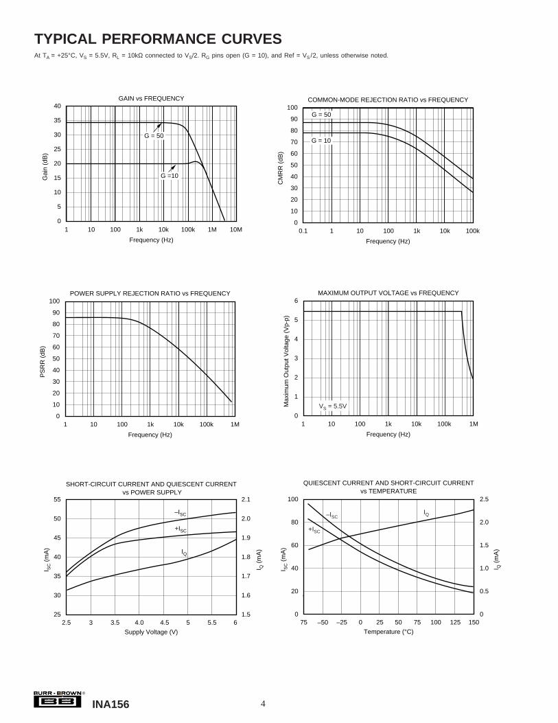
TYPICAL PERFORMANCE CURVESAt TA = +25°C, VS = 5.5V, RL = 10kΩ connected to VS/2. RG pins open (G = 10), and Ref = VS /2, unless otherwise noted.
GAIN vs FREQUENCY
Frequency (Hz)
Gai
n (d
B)
1 10010 1k 10k 1M 10M
40
35
30
25
20
15
10
5
0100k
G = 50
G =10
COMMON-MODE REJECTION RATIO vs FREQUENCY
Frequency (Hz)
CM
RR
(dB
)
0.1 1 10 10k 100k
100
90
80
70
60
50
40
30
20
10
0100 1k
G = 50
G = 10
POWER SUPPLY REJECTION RATIO vs FREQUENCY
Frequency (Hz)
PS
RR
(dB
)
1 10 10k 100k 1M
100
90
80
70
60
50
40
30
20
10
0100 1k
MAXIMUM OUTPUT VOLTAGE vs FREQUENCY
Frequency (Hz)
Max
imum
Out
put V
olta
ge (
Vp-
p)
1 10 10k 100k 1M
6
5
4
3
2
1
0100 1k
VS = 5.5V
SHORT-CIRCUIT CURRENT AND QUIESCENT CURRENT vs POWER SUPPLY
Supply Voltage (V)
I SC (
mA
)
2.5 3 4.03.5
55
50
45
40
35
30
25
I Q (
mA
)
2.1
2.0
1.9
1.8
1.7
1.6
1.54.5 5.5 6 5
IQ
+ISC
–ISC
QUIESCENT CURRENT AND SHORT-CIRCUIT CURRENTvs TEMPERATURE
Temperature (°C)
I Q (
mA
)
I SC (
mA
)
75 –50 0–25
2.5
2.0
1.5
1.0
0.5
0
100
80
60
40
20
025 100 125 15050 75
IQ
+ISC
–ISC
5®
INA156
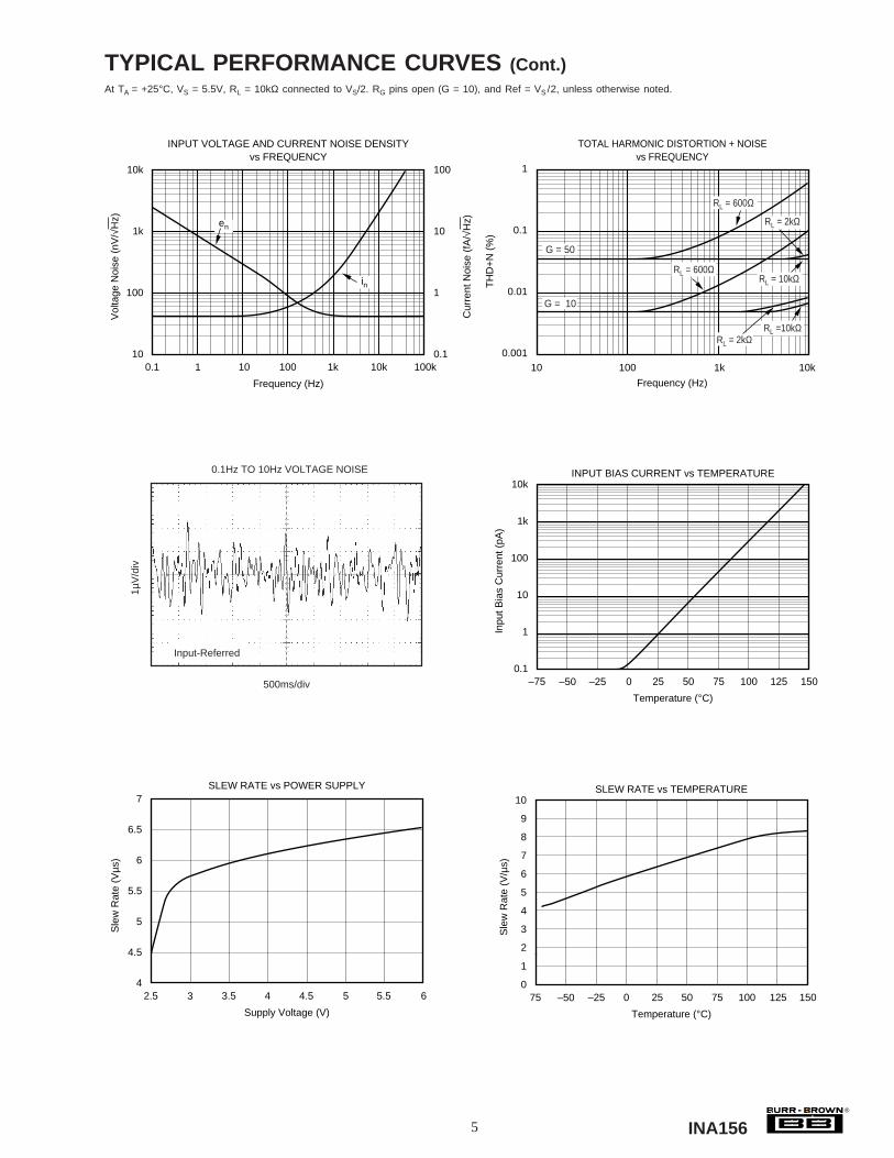
TYPICAL PERFORMANCE CURVES (Cont.)At TA = +25°C, VS = 5.5V, RL = 10kΩ connected to VS/2. RG pins open (G = 10), and Ref = VS /2, unless otherwise noted.
0.1Hz TO 10Hz VOLTAGE NOISE
500ms/div
1µV
/div
Input-Referred
INPUT VOLTAGE AND CURRENT NOISE DENSITYvs FREQUENCY
Frequency (Hz)
Vol
tage
Noi
se (
nV/√
Hz)
0.1 1 10
10k
1k
100
10
100
10
1
0.1100 100k1k 10k
Cur
rent
Noi
se (
fA/√
Hz)en
in
TOTAL HARMONIC DISTORTION + NOISEvs FREQUENCY
1
0.1
0.01
0.001
TH
D+
N (
%)
10 100 10k1k
Frequency (Hz)
RL = 600Ω
RL = 600ΩRL = 10kΩ
RL = 2kΩ
G = 50
G = 10
RL =10kΩRL = 2kΩ
SLEW RATE vs TEMPERATURE
Temperature (°C)
Sle
w R
ate
(V/µ
s)
75 –50 0–25
10
9
8
7
6
5
4
3
2
1
025 100 125 15050 75
SLEW RATE vs POWER SUPPLY
Supply Voltage (V)
Sle
w R
ate
(Vµs
)
2.5 3 43.5
7
6.5
6
5.5
5
4.5
44.5 65 5.5
INPUT BIAS CURRENT vs TEMPERATURE
Temperature (°C)
Inpu
t Bia
s C
urre
nt (
pA)
–75 –50 –25 0
10k
1k
100
10
1
0.125 100 125 15050 75

6®
INA156
TYPICAL PERFORMANCE CURVES (Cont.)At TA = +25°C, VS = 5.5V, RL = 10kΩ connected to VS/2. RG pins open (G = 10), and Ref = VS /2, unless otherwise noted.
5µs/div
100m
V/d
iv
SMALL-SIGNAL STEP RESPONSEG = 10, CL = 100pF, RL = 10kΩ
5µs/div
100m
V/d
iv
SMALL-SIGNAL STEP RESPONSEG = 50, CL = 100pF, RL = 10kΩ
OVERSHOOT vs LOAD CAPACITANCE
Load Capacitance (pF)
Ove
rsho
ot (
%)
10 100 10k
60
50
40
30
20
10
01k
G = 10
G = 50
SETTLING TIME vs LOAD CAPACITANCE
Load Capacitance (pF)
Set
tling
Tim
e (µ
s)
10 100 10k
20
18
16
14
12
10
8
6
4
2
01k
0.01%, G = 50
0.1%, G = 50
0.01%, G = 10
0.1%, G = 10
VOS TYPICALPRODUCTION DISTRIBUTION
Pro
duct
ion
Dis
trib
utio
n (%
)
Offset Voltage (mV)
–10 –8 –6 –4 –2 0 2 4 6 8 10
18
16
14
12
10
8
6
4
2
0
OFFSET VOLTAGE DRIFTPRODUCTION DISTRIBUTION
Per
cent
of A
mpl
ifier
s (%
)
Offset Voltage Drift (µV/°C)
–20
–18
–16
–14
–12
–10 –8 –6 –4 –2 0 2 4 6 8 10 12 14 16 18 20
18
16
14
12
10
8
6
4
2
0
7®
INA156
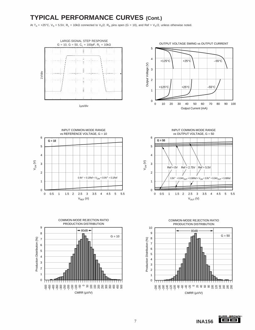
TYPICAL PERFORMANCE CURVES (Cont.)At TA = +25°C, VS = 5.5V, RL = 10kΩ connected to VS/2. RG pins open (G = 10), and Ref = VS /2, unless otherwise noted.
1µs/div
1V/d
ivLARGE-SIGNAL STEP RESPONSE
G = 10, G = 50, CL = 100pF, RL = 10kΩ
INPUT COMMON-MODE RANGEvs OUTPUT VOLTAGE, G = 50
VOUT (V)
VC
M (
V)
0 0.5 1 21.5
6
5
4
3
2
1
02.5 5.53 3.5 4 4.5 5
Ref = 0V Ref = 2.75V Ref = 5.5V
G = 50
0.9V– + 0.04VOUT + 0.06Ref < VCM < 0.9V+ + 0.04VOUT + 0.06Ref
INPUT COMMON-MODE RANGEvs REFERENCE VOLTAGE, G = 10
VREF (V)
VC
M (
V)
0 0.5 1 21.5
6
5
4
3
2
1
02.5 5.53 3.5 4 4.5 5
G = 10
0.9V– + 0.1Ref < VCM < 0.9V+ + 0.1Ref
COMMON-MODE REJECTION RATIOPRODUCTION DISTRIBUTION
Pro
duct
ion
Dis
trib
utio
n (%
)
CMRR (µV/V)
G = 10
80dB
–500
–450
–400
–350
–300
–250
–200
–150
–100 –50 0 50 100
150
200
250
300
350
400
450
500
9
8
7
6
5
4
3
2
1
0
COMMON-MODE REJECTION RATIOPRODUCTION DISTRIBUTION
Pro
duct
ion
Dis
trib
utio
n (%
)
CMRR (µV/V)
G = 50
–200
–180
–160
–140
–120
–100 –80
–60
–40
–20 0 20 40 60 80 100
120
140
160
180
200
10
9
8
7
6
5
4
3
2
1
0
80dB
OUTPUT VOLTAGE SWING vs OUTPUT CURRENT
Output Current (mA)
Out
put V
olta
ge (
V)
5
4
3
2
1
00 10 20 30 40 50 60 70 80 90 100
+125°C +25°C –55°C
+125°C +25°C –55°C

8®
INA156
APPLICATIONS INFORMATIONFigure 1 shows the basic connections required for operationof the INA156. Applications with noisy or high impedancepower supplies may require decoupling capacitors close tothe device pins, as shown.
The output is referred to the output reference terminal, Ref,which is normally set to VS/2. This must be a low-imped-ance connection to ensure good common-mode rejection.
In addition, for the G = 50 configuration, the connectionbetween pins 1 and 8 must be low-impedance. A connectionimpedance of 20Ω can cause a 0.2% shift in gain error.
OPERATING VOLTAGE
The INA156 is fully specified and guaranteed over the supplyrange +2.7V to +5.5V, with key parameters guaranteed overthe temperature range of –55°C to +125°C. Parameters thatvary significantly with operating voltages, load conditions ortemperature are shown in the Typical Performance Curves.
The INA156 can be operated from either single or dualpower supplies. By adjusting the voltage applied to thereference terminal, the input common-mode voltage rangeand the output range can be adjusted within the boundsshown in the Typical Performance Curves. Figure 2 showsa bridge amplifier circuit operated from a single +5V powersupply. The bridge provides a relatively small differentialvoltage on top of an input common-mode voltage near 2.5V.
FIGURE 1. Basic Connections.
FIGURE 2. Single-Supply Bridge Amplifier.
Ref22.2kΩ200kΩ
5kΩ
Gain Pins Open:G = 10
External Resistor RG:10 < G < 50
Gain Pins Connected:G = 50
5kΩ
200kΩ22.2kΩ
4
3
2
5
71 8
V–
0.1µF
Single Supply
Also drawn in simplified form:
Dual Supply
INA156
INA156
6
1
3
8
2
VOUT6
7
4
5
Ref
0.1µF
V+
V+
V–
DESIRED GAIN RG(V/V) (Ω)
10 Open20 30k30 10k40 3.3k50 Short
G = 10 + 400kΩ
10kΩ + RG
VIN–
VIN+
A1
A2
VIN+
VIN–
VOUT = (VIN – VIN) • G + VREF+ –
BridgeSensor
INA156
VREF(1)
+5V
3
2
4
5
76
VOUT = 0.01V to 4.99V
(2)
NOTES: (1) VREF should be adjusted for the desired output level, keeping in mind that the value of VREF affects the common-mode input range. See Typical Performance Curves. (2) For best performance, the common-mode input voltage should be kept away from the transition range of (V+) – 1.8V to (V+) – 0.8V.
1
8
VIN+
VIN–

9®
INA156
SETTING THE GAIN
Gain of 10 is achieved simply by leaving the two gain pins(1 and 8) open. Gain of 50 is achieved by connecting thegain pins together directly. In the G = 10 configuration, thegain error is less than 0.4%. In the G = 50 configuration, thegain error is less than 0.8%.
Gain can be set to any value between 10 and 50 by connect-ing a resistor RG between the gain pins according to thefollowing equation:
10 + 400kΩ/(10kΩ + RG) (1)
This is demonstrated in Figure 1 and is shown with the com-monly used gains and resistor RG values. However, because theabsolute value of internal resistors is not guaranteed, using theINA156 in this configuration will increase the gain error andgain drift with temperature, as shown in Figure 3.
FIGURE 3. Typical Gain Error and Gain Error Drift withExternal Resistor.
OFFSET TRIMMING
Offset voltage can be adjusted by applying a correctionvoltage to the reference terminal. Figure 4 shows an optionalcircuit for trimming the output offset voltage. The voltageapplied to the Ref terminal is added to the output signal. Anop amp buffer is used to provide low impedance at the Refterminal to preserve good common-mode rejection.
INPUT BIAS CURRENT RETURN
The input impedance of the INA156 is extremely high—approximately 1013Ω, making it ideal for use with high-imped-ance sources. However, a path must be provided for the inputbias current of both inputs. This input bias current is less than10pA and is virtually independent of the input voltage.
Input circuitry must provide a path for this input bias currentfor proper operation. Figure 5 shows various provisions foran input bias current path. Without a bias current path, theinputs will float to a potential that exceeds the common-mode range and the input amplifier will saturate.
If the differential source resistance is low, the bias currentreturn path can be connected to one input (see the thermo-couple in Figure 5). With higher source impedance, usingtwo equal resistors provides a balanced input with advan-tages of lower input offset voltage due to bias current andbetter high-frequency common-mode rejection.
FIGURE 4. Optional Trimming of Output Offset Voltage. FIGURE 5. Providing an Input Common-Mode Current Path.
Gain (V/V)
Gai
n E
rror
(%
)
10 15 20 3025
2.0
1.8
1.6
1.4
1.2
1.0
0.8
0.6
0.4
0.2
0
Gai
n D
rift (
ppm
/°C
)
400
360
320
280
250
200
160
120
80
40
035 40 5045
Gain Drift
Gain Error
OPA336
INA156
Ref(1)
3
6
2 5
VO
AdjustableVoltage
VIN+(2)
VIN–(2)
NOTES: (1) VREF should be adjusted for the desired output level. The value of VREF affects the common-mode input range. (2) For best performance, common-mode input voltage should be less than (V+) – 1.8V or greater than (V+) – 0.8V.
1
8
INA156
3
6
6
6
6
247kΩ
5
VREF
47kΩ
Microphone,Hydrophone, etc.
INA156
3
2
3
2
5
VREF
Center-tapprovides biascurrent return
Low-resistancethermocoupleprovides biascurrent return.
Bridge resistanceprovides biascurrent return
INA156
3
2
10kΩ
5
VREF
Thermocouple
INA156
5
VREF
BridgeSensor
1
8
1
8
1
8
1
8

10®
INA156
FIGURE 6. Input Offset Voltage Changes with Common-Mode Voltage.
FIGURE 7. Single-Supply, High-Side Current Monitor.
FIGURE 8. Input Current Protection for Voltages Exceed-ing the Supply Voltage.
FIGURE 9. Driving Capacitive-Input A/D Converter.
INPUT COMMON-MODE RANGE
The input common-mode range of the INA156 for variousoperating conditions is shown in the Typical PerformanceCurves. The common-mode input range is limited by theoutput voltage swing of A1, an internal circuit node. For theG = 10 configuration, output voltage of A1 can be expressed as:
VOUTA1 = – 1/9VREF + (1 + 1/9) VIN– (2)
The input common-mode voltage range can be calculatedusing this equation, given that the output of A1 can swing towithin 20mV of either rail. When the input common-moderange is exceeded (A1’s output is saturated), A2 can still be inlinear operation and respond to changes in the non-invertinginput voltage. However, the output voltage will be invalid.
The common-mode range for the G = 50 configuration isincluded in the typical performance curve, “Input Common-Mode Range vs Output Voltage.”
INPUT RANGE FOR BEST ACCURACY
The internal amplifiers have rail-to-rail input stages, achievedby using complementary n-channel and p-channel inputpairs. The common-mode input voltage determines whetherthe p-channel or the n-channel input stage is operating. Thetransition between the input stages is gradual and occursbetween (V+) – 1.8V to (V+) – 1V. Due to these character-istics, operating the INA156 with input voltages within thetransition region of (V+) – 1.8V to (V+) – 0.8V results in ashift in input offset voltage, and reduced common-mode andpower supply rejection performance. Typical patterns of theoffset voltage change throughout the input common-moderange are illustrated in Figure 6. The INA156 can beoperated below or above the transition region with excellentresults. Figure 7 demonstrates the use of the INA156 in asingle-supply, high-side current monitor. In this application,the INA156 is operated above the transition region.
RAIL-TO-RAIL OUTPUT
A class AB output stage with common-source transistors isused to achieve rail-to-rail output. For resistive loadsgreater than 10kΩ, the output voltage can swing to withina few millivolts of the supply rail while maintaining lowgain error. For heavier loads and over temperature, see thetypical performance curve “Output Voltage Swing vs Out-put Current.” The INA156’s low output impedance at highfrequencies makes it suitable for directly driving Capaci-tive Digital-to-Analog (CDAC) input A/D converters, asshown in Figure 9.
INPUT PROTECTION
Device inputs are protected by ESD diodes that will conductif the input voltages exceed the power supplies by more than500mV. Momentary voltages greater than 500mV beyondthe power supply can be tolerated if the current on the inputpins is limited to 10mA. This is easily accomplished withinput resistors RLIM , as shown in Figure 8. Many inputsignals are inherently current-limited to less than 10mA.Therefore, a limiting resistor is not required.
INA156
76
4
5Ref
IL2.5A
G = 10Pins 1 and 8 Open
V+ NOTE: Output is referred to V+.
2
3
1
8
0.02Ω
Load
50mV
+5V
INA156ADS7818
orADS7834
12-Bits
fSAMPLE = 500kHz
6
7
4
5
3
2
NOTE: G = 10 configuration
1
8
INA156
5
VOUT
VREF
RLIM
RLIM
IOVERLOAD10mA max
3
6
2
1
8
Input Common-Mode Voltage (V)
Inpu
t Offs
et V
olta
ge (
mV
)
0.0 0.5 1.0 2.5 3.01.5 2.0
5
4
3
2
1
0
–1
–2
–3
–4
–53.5 4.0 4.5 5.55.0
VS = 5.5V
P-Channel Operation TransistionRegion N-Channel
Operation
PACKAGE OPTION ADDENDUM
www.ti.com 11-Jul-2013
Addendum-Page 1
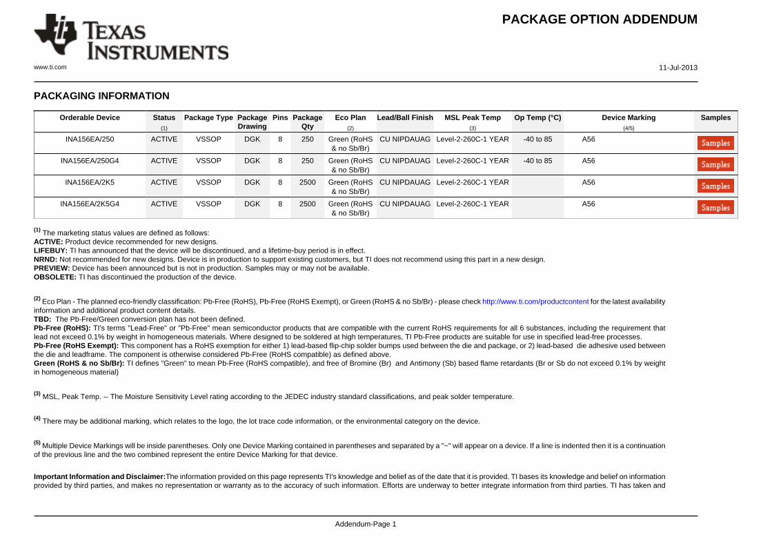
PACKAGING INFORMATION
Orderable Device Status(1)
Package Type PackageDrawing
Pins PackageQty
Eco Plan(2)
Lead/Ball Finish MSL Peak Temp(3)
Op Temp (°C) Device Marking(4/5)
Samples
INA156EA/250 ACTIVE VSSOP DGK 8 250 Green (RoHS& no Sb/Br)
CU NIPDAUAG Level-2-260C-1 YEAR -40 to 85 A56
INA156EA/250G4 ACTIVE VSSOP DGK 8 250 Green (RoHS& no Sb/Br)
CU NIPDAUAG Level-2-260C-1 YEAR -40 to 85 A56
INA156EA/2K5 ACTIVE VSSOP DGK 8 2500 Green (RoHS& no Sb/Br)
CU NIPDAUAG Level-2-260C-1 YEAR A56
INA156EA/2K5G4 ACTIVE VSSOP DGK 8 2500 Green (RoHS& no Sb/Br)
CU NIPDAUAG Level-2-260C-1 YEAR A56
(1) The marketing status values are defined as follows:ACTIVE: Product device recommended for new designs.LIFEBUY: TI has announced that the device will be discontinued, and a lifetime-buy period is in effect.NRND: Not recommended for new designs. Device is in production to support existing customers, but TI does not recommend using this part in a new design.PREVIEW: Device has been announced but is not in production. Samples may or may not be available.OBSOLETE: TI has discontinued the production of the device.
(2) Eco Plan - The planned eco-friendly classification: Pb-Free (RoHS), Pb-Free (RoHS Exempt), or Green (RoHS & no Sb/Br) - please check http://www.ti.com/productcontent for the latest availabilityinformation and additional product content details.TBD: The Pb-Free/Green conversion plan has not been defined.Pb-Free (RoHS): TI's terms "Lead-Free" or "Pb-Free" mean semiconductor products that are compatible with the current RoHS requirements for all 6 substances, including the requirement thatlead not exceed 0.1% by weight in homogeneous materials. Where designed to be soldered at high temperatures, TI Pb-Free products are suitable for use in specified lead-free processes.Pb-Free (RoHS Exempt): This component has a RoHS exemption for either 1) lead-based flip-chip solder bumps used between the die and package, or 2) lead-based die adhesive used betweenthe die and leadframe. The component is otherwise considered Pb-Free (RoHS compatible) as defined above.Green (RoHS & no Sb/Br): TI defines "Green" to mean Pb-Free (RoHS compatible), and free of Bromine (Br) and Antimony (Sb) based flame retardants (Br or Sb do not exceed 0.1% by weightin homogeneous material)
(3) MSL, Peak Temp. -- The Moisture Sensitivity Level rating according to the JEDEC industry standard classifications, and peak solder temperature.
(4) There may be additional marking, which relates to the logo, the lot trace code information, or the environmental category on the device.
(5) Multiple Device Markings will be inside parentheses. Only one Device Marking contained in parentheses and separated by a "~" will appear on a device. If a line is indented then it is a continuationof the previous line and the two combined represent the entire Device Marking for that device.
Important Information and Disclaimer:The information provided on this page represents TI's knowledge and belief as of the date that it is provided. TI bases its knowledge and belief on informationprovided by third parties, and makes no representation or warranty as to the accuracy of such information. Efforts are underway to better integrate information from third parties. TI has taken and
PACKAGE OPTION ADDENDUM
www.ti.com 11-Jul-2013
Addendum-Page 2
continues to take reasonable steps to provide representative and accurate information but may not have conducted destructive testing or chemical analysis on incoming materials and chemicals.TI and TI suppliers consider certain information to be proprietary, and thus CAS numbers and other limited information may not be available for release.
In no event shall TI's liability arising out of such information exceed the total purchase price of the TI part(s) at issue in this document sold by TI to Customer on an annual basis.

TAPE AND REEL INFORMATION
*All dimensions are nominal
Device PackageType
PackageDrawing
Pins SPQ ReelDiameter
(mm)
ReelWidth
W1 (mm)
A0(mm)
B0(mm)
K0(mm)
P1(mm)
W(mm)
Pin1Quadrant
INA156EA/250 VSSOP DGK 8 250 180.0 12.4 5.3 3.4 1.4 8.0 12.0 Q1
INA156EA/2K5 VSSOP DGK 8 2500 330.0 12.4 5.3 3.4 1.4 8.0 12.0 Q1
PACKAGE MATERIALS INFORMATION
www.ti.com 26-Jan-2013
Pack Materials-Page 1
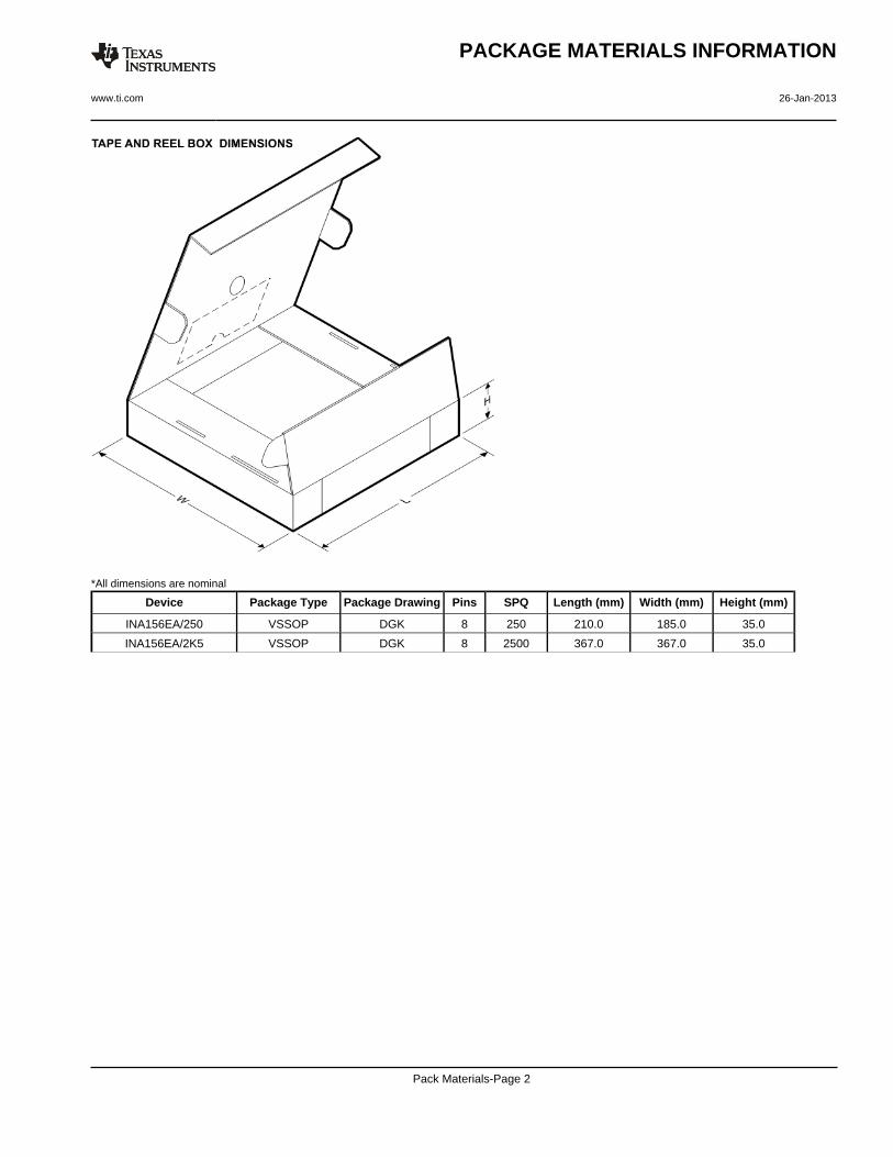
*All dimensions are nominal
Device Package Type Package Drawing Pins SPQ Length (mm) Width (mm) Height (mm)
INA156EA/250 VSSOP DGK 8 250 210.0 185.0 35.0
INA156EA/2K5 VSSOP DGK 8 2500 367.0 367.0 35.0
PACKAGE MATERIALS INFORMATION
www.ti.com 26-Jan-2013
Pack Materials-Page 2

IMPORTANT NOTICE
Texas Instruments Incorporated and its subsidiaries (TI) reserve the right to make corrections, enhancements, improvements and otherchanges to its semiconductor products and services per JESD46, latest issue, and to discontinue any product or service per JESD48, latestissue. Buyers should obtain the latest relevant information before placing orders and should verify that such information is current andcomplete. All semiconductor products (also referred to herein as “components”) are sold subject to TI’s terms and conditions of salesupplied at the time of order acknowledgment.
TI warrants performance of its components to the specifications applicable at the time of sale, in accordance with the warranty in TI’s termsand conditions of sale of semiconductor products. Testing and other quality control techniques are used to the extent TI deems necessaryto support this warranty. Except where mandated by applicable law, testing of all parameters of each component is not necessarilyperformed.
TI assumes no liability for applications assistance or the design of Buyers’ products. Buyers are responsible for their products andapplications using TI components. To minimize the risks associated with Buyers’ products and applications, Buyers should provideadequate design and operating safeguards.
TI does not warrant or represent that any license, either express or implied, is granted under any patent right, copyright, mask work right, orother intellectual property right relating to any combination, machine, or process in which TI components or services are used. Informationpublished by TI regarding third-party products or services does not constitute a license to use such products or services or a warranty orendorsement thereof. Use of such information may require a license from a third party under the patents or other intellectual property of thethird party, or a license from TI under the patents or other intellectual property of TI.
Reproduction of significant portions of TI information in TI data books or data sheets is permissible only if reproduction is without alterationand is accompanied by all associated warranties, conditions, limitations, and notices. TI is not responsible or liable for such altereddocumentation. Information of third parties may be subject to additional restrictions.
Resale of TI components or services with statements different from or beyond the parameters stated by TI for that component or servicevoids all express and any implied warranties for the associated TI component or service and is an unfair and deceptive business practice.TI is not responsible or liable for any such statements.
Buyer acknowledges and agrees that it is solely responsible for compliance with all legal, regulatory and safety-related requirementsconcerning its products, and any use of TI components in its applications, notwithstanding any applications-related information or supportthat may be provided by TI. Buyer represents and agrees that it has all the necessary expertise to create and implement safeguards whichanticipate dangerous consequences of failures, monitor failures and their consequences, lessen the likelihood of failures that might causeharm and take appropriate remedial actions. Buyer will fully indemnify TI and its representatives against any damages arising out of the useof any TI components in safety-critical applications.
In some cases, TI components may be promoted specifically to facilitate safety-related applications. With such components, TI’s goal is tohelp enable customers to design and create their own end-product solutions that meet applicable functional safety standards andrequirements. Nonetheless, such components are subject to these terms.
No TI components are authorized for use in FDA Class III (or similar life-critical medical equipment) unless authorized officers of the partieshave executed a special agreement specifically governing such use.
Only those TI components which TI has specifically designated as military grade or “enhanced plastic” are designed and intended for use inmilitary/aerospace applications or environments. Buyer acknowledges and agrees that any military or aerospace use of TI componentswhich have not been so designated is solely at the Buyer's risk, and that Buyer is solely responsible for compliance with all legal andregulatory requirements in connection with such use.
TI has specifically designated certain components as meeting ISO/TS16949 requirements, mainly for automotive use. In any case of use ofnon-designated products, TI will not be responsible for any failure to meet ISO/TS16949.
Products Applications
Audio www.ti.com/audio Automotive and Transportation www.ti.com/automotive
Amplifiers amplifier.ti.com Communications and Telecom www.ti.com/communications
Data Converters dataconverter.ti.com Computers and Peripherals www.ti.com/computers
DLP® Products www.dlp.com Consumer Electronics www.ti.com/consumer-apps
DSP dsp.ti.com Energy and Lighting www.ti.com/energy
Clocks and Timers www.ti.com/clocks Industrial www.ti.com/industrial
Interface interface.ti.com Medical www.ti.com/medical
Logic logic.ti.com Security www.ti.com/security
Power Mgmt power.ti.com Space, Avionics and Defense www.ti.com/space-avionics-defense
Microcontrollers microcontroller.ti.com Video and Imaging www.ti.com/video
RFID www.ti-rfid.com
OMAP Applications Processors www.ti.com/omap TI E2E Community e2e.ti.com
Wireless Connectivity www.ti.com/wirelessconnectivity
Mailing Address: Texas Instruments, Post Office Box 655303, Dallas, Texas 75265Copyright © 2013, Texas Instruments Incorporated