six channel delta sigma a/d converterww1.microchip.com/downloads/en/devicedoc/25048b.pdfsampling...
TRANSCRIPT

MCP3903Six Channel Delta Sigma A/D Converter
Features• Six Synchronous Sampling 16/24-bit Resolution
Delta-Sigma A/D Converters with Proprietary Multi-Bit Architecture
• 91 dB SINAD, -100 dBc Total Harmonic Distortion (THD) (up to 35th harmonic), 102 dB Spurious-free Dynamic Range (SFDR) for Each Channel
• Programmable Data Rate up to 64 ksps• Ultra Low-Power Shutdown Mode with <2 μA• -115 dB Crosstalk Between any Two Channels• Low Drift Internal Voltage Reference: 5 ppm/°C• Differential Voltage Reference Input Pins• High Gain PGA on Each Channel (up to 32 V/V)• Phase Delay Compensation Between Each Pair
of Channels with 1 μs Time Resolution• High-Speed Addressable 10 MHz SPI Interface
with Mode 0,0 and 1,1 Compatibility• Independent Analog and Digital Power Supplies
4.5V - 5.5V AVDD, 2.7V - 3.6V DVDD• Available in Small 28-lead SSOP Package• Extended Temperature Range: -40°C to +125°C
Applications• Energy Metering and Power Measurement• Portable Instrumentation• Medical and Power Monitoring
DescriptionThe MCP3903 is a six-channel Analog Front End (AFE)containing three pairs made out of two synchronoussampling Delta-Sigma Analog-to-Digital Converters(ADC) with PGA, a phase delay compensation block,internal voltage reference, and high-speed 10 MHz SPIcompatible serial interface. The converters contain aproprietary dithering algorithm for reduced idle tonesand improved THD.
The internal register map contains 24-bit wide ADCdata words, a modulator output register as well as six24-bit writable control registers to program gain,over-sampling ratio, phase, resolution, dithering,shut-down, reset and several communication features.
The communication is largely simplified with variousContinuous Read modes that can be accessed by theDirect Memory Access (DMA) of an MCU and withseparate Data Ready pins that can directly beconnected to the Interrupt Request (IRQ) input of anMCU. The MCP3903 is capable of interfacing to a largevariety of voltage and current sensors including shunts,current transformers, Rogowski coils, and Hall-effectsensors.
Package Type
CS
1234
2827262524232221
5678
SCK
DVDDAVDDCH0+CH0-CH1-CH1+CH2+
209DRB
OSC1DRC
OSC2CH2-CH3-
RESET
1910
CH3+
CH4+
SDOSDI
28-Lead SSOP
1817
1112
1613REFIN-
DGNDAGND
DRACH4-CH5-
1514
CH5+
REFIN/OUT+
© 2011 Microchip Technology Inc. DS25048B-page 1

MCP3903
Functional Block DiagramCH0+CH0-
CH1+CH1-
SDO
SDISCK
DUAL DS ADC
ANALOG DIGITAL
SINC3-+
PGA
Xtal OscillatorMCLK OSC1
OSC2
DRA
RESET
Digital SPI Interface
Clock Generation
SINC3
-+
PGAModulator
AMCLK
DMCLK/DRCLK
DMCLK
Phase Shifter
PHASEA <7:0>
OSR<1:0>PRE<1:0>
DATA_CH0<23:0>
DATA_CH1<23:0>
CS
REFIN/OUT+
REFIN -
AVDD
AGND DGND
DVDD
PORAVDD
Monitoring
Modulator
VREF+VREF-
VREFEXTVoltage Reference
VREF+-
Δ -Σ
Δ -Σ
Φ
CH2+CH2-
CH3+CH3-
DUAL DS ADC
SINC3-+
PGA
SINC3
-+
PGAModulator Phase
ShifterPHASEB <7:0>
DATA_CH2<23:0>
DATA_CH3<23:0>
ModulatorΔ -Σ
Δ -Σ
Φ
CH4+CH4-
CH5+CH5-
DUAL DS ADC
SINC3-+
PGA
SINC3
-+
PGAModulator Phase
ShifterPHASEC <7:0>
DATA_CH4<23:0>
DATA_CH5<23:0>
ModulatorΔ -Σ
Δ -Σ
Φ
DRB
DRC
POR
DS25048B-page 2 © 2011 Microchip Technology Inc.

MCP3903
1.0 ELECTRICAL CHARACTERISTICS
The Reliability Targets section includes the absolutemaximum ratings for the device, defining the valuesthat will cause no long term damage regardless ofduration.
These tables also represent the testing requirementsper the Max. and Min. columns.
1.1 RELIABILITY TARGETS
ABSOLUTE MAXIMUM RATINGS †VDD ................................................................................... 7.0VDigital inputs and outputs w.r.t. AGND ........-0.6V to VDD +0.6VAnalog input w.r.t. AGND..................................... ....-6V to +6VVREF input w.r.t. AGND................................-0.6V to VDD +0.6VStorage temperature..................................... -65°C to +150°CAmbient temp. with power applied................ -65°C to +125°CSoldering temperature of leads (10 seconds)............. +300°CESD on the analog inputs (HBM,MM)................. 5.0 kV, 500VESD on all other pins (HBM,MM)........................ 5.0 kV, 500V
TABLE 1-1: ANALOG SPECIFICATIONS TARGET TABLEElectrical Specifications: Unless otherwise indicated, all parameters apply at AVDD = 4.5 to 5.5V, DVDD = 2.7 to 3.6V, Internal VREF, MCLK = 4 MHz;PRESCALE = 1; OSR = 64; fS = 1 MHz; fD = 15.625 ksps; TA = -40°C to +125°C, GAIN = 1, VIN = 1VPP = 353mVRMS @ 50/60 Hz.
Param. Num. Symbol Characteristic Min. Typ. Max. Units Test Conditions
Internal Voltage Reference
A001 VREF Voltage -2% 2.35 +2% V VREFEXT = 0A002 TCREF Tempco — 5 — ppm/°C VREFEXT = 0A003 ZOUTREF Output Impedance 7 — kΩ AVDD=5V,
VREFEXT = 0Voltage Reference InputA004 Input Capacitance — — 10 pFA005 VREF Differential Input Voltage
Range (VREF+ - VREF-) 2.2 — 2.6 V VREF = (VREF+ - VREF-),
VREFEXT = 1A006 VREF+ Absolute Voltage on REFIN+
pin1.9 — 2.9 V VREFEXT = 1
A007 VREF- Absolute Voltage on REFIN- pin
-0.3 — +0.3 V VREF- should be connected to AGND when VREFEXT=0
ADC PerformanceA008 Resolution (No Missing
Codes)24 bits OSR = 256 (see Table 5-2)
A009 fS Sampling Frequency See Table 4-2 kHz fS = DMCLK = MCLK / (4 x PRESCALE)
A010 fD Output Data Rate See Table 4-2 ksps fD = DRCLK= DMCLK / OSR = MCLK / (4 x PRESCALE x OSR)
Note 1: This specification implies that the ADC output is valid over this entire differential range, i.e. there is no distortion or instability across this input range. Dynamic Performance is specified at -0.5 dB below the maximum signal range,VIN = -0.5 dBFS @ 50/60 Hz = 333 mVRMS, VREF = 2.4V.
2: See terminology section for definition.3: This parameter is established by characterization and not 100% tested.4: For these operating currents, the following configuration bit settings apply: Config Register Settings:
SHUTDOWN<5:0> = 000000, RESET<5:0> = 000000; VREFEXT = 0, CLKEXT = 0.5: For these operating currents, the following configuration bit settings apply: Config Register Settings:
SHUTDOWN<5:0> = 111111, VREFEXT = 1, CLKEXT = 1.6: Applies to all gains. Offset error is dependant on PGA gain setting.7: Outside of this range, ADC accuracy is not specified. An extended input range of +/- 6V can be applied continuously to
the part with no risk for damage.8: For proper operation and to keep ADC accuracy, AMCLK should always be in the range of 1 to 5 MHz with BOOST bits
off. With BOOST bits on, AMCLK should be in the range of 1 to 8.192 MHz. AMCLK = MCLK/PRESCALE. When using a crystal, CLKEXT bit should be equal to ‘0’.
© 2011 Microchip Technology Inc. DS25048B-page 3

MCP3903
A011 CHn+- Analog Input Absolute Voltage
-1 +1 V All analog input channels, measured to AGND (Note 7)
A012 AIN Analog Input Leakage Current
1 nA (Note 4)
A013 (CHn+-CHn-)
Differential Input Voltage Range
500 / GAIN
mVP (Note 1)
A014 VOS Offset Error -3 3 mV (Note 6)(Note 2)A015 Offset Error Drift 1 μV/C From -40°C to 125°CA016 GE Gain Error -3 3 % All GainsA017 Gain Error Drift — 2 — ppm/°C From -40°C to 125°CA018 INL Integral Non-Linearity 15 ppm GAIN = 1, DITHER = ONA019 ZIN Input Impedance 350 — — kΩ Proportional to 1/AMCLK A020 SINAD Signal-to-Noise and
Distortion Ratio89 91 — dB T = 25°C80 81.5 dB
A021 THD Total Harmonic Distortion -100 -97 dB OSR = 256, DITHER = ON; (Note 2)(Note 3)
-90 -87 dBA022 SNR Signal To Noise Ratio 90 91.5 dB T = 25°C
80 81.5 dBA023 SFDR Spurious Free Dynamic
Range102 dB OSR = 256, DITHER = ON;
(Note 2) (Note 3)91 dB
A024 CTALK Crosstalk (50 / 60 Hz) — -115 — dB OSR = 256, DITHER = ON; (Note 2)(Note 3)
A025 AC PSRR AC Power Supply Rejection — -68 — dB AVDD = 5V + 1Vpp @ 50 HzA026 DC PSRR DC Power Supply Rejection — -68 — dB AVDD = 4.5 to 5.5V, DVDD =
3.3VA027 CMRR DC Common Mode Rejection
Ratio— -75 — dB VCM varies from -1V to +1V;
(Note 2)Oscillator Input
TABLE 1-1: ANALOG SPECIFICATIONS TARGET TABLE (CONTINUED)Electrical Specifications: Unless otherwise indicated, all parameters apply at AVDD = 4.5 to 5.5V, DVDD = 2.7 to 3.6V, Internal VREF, MCLK = 4 MHz;PRESCALE = 1; OSR = 64; fS = 1 MHz; fD = 15.625 ksps; TA = -40°C to +125°C, GAIN = 1, VIN = 1VPP = 353mVRMS @ 50/60 Hz.
Param. Num. Symbol Characteristic Min. Typ. Max. Units Test Conditions
Note 1: This specification implies that the ADC output is valid over this entire differential range, i.e. there is no distortion or instability across this input range. Dynamic Performance is specified at -0.5 dB below the maximum signal range,VIN = -0.5 dBFS @ 50/60 Hz = 333 mVRMS, VREF = 2.4V.
2: See terminology section for definition.3: This parameter is established by characterization and not 100% tested.4: For these operating currents, the following configuration bit settings apply: Config Register Settings:
SHUTDOWN<5:0> = 000000, RESET<5:0> = 000000; VREFEXT = 0, CLKEXT = 0.5: For these operating currents, the following configuration bit settings apply: Config Register Settings:
SHUTDOWN<5:0> = 111111, VREFEXT = 1, CLKEXT = 1.6: Applies to all gains. Offset error is dependant on PGA gain setting.7: Outside of this range, ADC accuracy is not specified. An extended input range of +/- 6V can be applied continuously to
the part with no risk for damage.8: For proper operation and to keep ADC accuracy, AMCLK should always be in the range of 1 to 5 MHz with BOOST bits
off. With BOOST bits on, AMCLK should be in the range of 1 to 8.192 MHz. AMCLK = MCLK/PRESCALE. When using a crystal, CLKEXT bit should be equal to ‘0’.
DS25048B-page 4 © 2011 Microchip Technology Inc.

MCP3903
A028 MCLK Master Clock Frequency Range
1 — 16.384 MHz (Note 8)
Power SpecificationsP001 AVDD Operating Voltage, Analog 4.5 — 5.5 VP002 DVDD Operating Voltage, Digital 2.7 — 3.6 V P003 AIDD Operating Current, Analog
(Note 4)7.1 9 mA BOOST bits low on all chan-
nels12.3 16.8 mA BOOST bits high on all
channelsP004 DIDD Operating Current, Digital — 1.2 1.7 mA DVDD = 3.6V, MCLK =
4 MHz— 2.4 3.4 mA DVDD = 3.6V, MCLK =
8.192 MHzP005 IDDS,A Shutdown Current, Analog — — 1 μA -40°C to 85°C, AVDD pin
only, (Note 5)— — 3 μA -40°C to 125°C, AVDD pin
only, (Note 5)P006 IDDS,D Shutdown Current, Digital — — 1 μA -40°C to 85°C, DVDD pin
only, (Note 5)— — 5 μA -40°C to 125°C, DVDD pin
only, (Note 5)
TABLE 1-1: ANALOG SPECIFICATIONS TARGET TABLE (CONTINUED)Electrical Specifications: Unless otherwise indicated, all parameters apply at AVDD = 4.5 to 5.5V, DVDD = 2.7 to 3.6V, Internal VREF, MCLK = 4 MHz;PRESCALE = 1; OSR = 64; fS = 1 MHz; fD = 15.625 ksps; TA = -40°C to +125°C, GAIN = 1, VIN = 1VPP = 353mVRMS @ 50/60 Hz.
Param. Num. Symbol Characteristic Min. Typ. Max. Units Test Conditions
Note 1: This specification implies that the ADC output is valid over this entire differential range, i.e. there is no distortion or instability across this input range. Dynamic Performance is specified at -0.5 dB below the maximum signal range,VIN = -0.5 dBFS @ 50/60 Hz = 333 mVRMS, VREF = 2.4V.
2: See terminology section for definition.3: This parameter is established by characterization and not 100% tested.4: For these operating currents, the following configuration bit settings apply: Config Register Settings:
SHUTDOWN<5:0> = 000000, RESET<5:0> = 000000; VREFEXT = 0, CLKEXT = 0.5: For these operating currents, the following configuration bit settings apply: Config Register Settings:
SHUTDOWN<5:0> = 111111, VREFEXT = 1, CLKEXT = 1.6: Applies to all gains. Offset error is dependant on PGA gain setting.7: Outside of this range, ADC accuracy is not specified. An extended input range of +/- 6V can be applied continuously to
the part with no risk for damage.8: For proper operation and to keep ADC accuracy, AMCLK should always be in the range of 1 to 5 MHz with BOOST bits
off. With BOOST bits on, AMCLK should be in the range of 1 to 8.192 MHz. AMCLK = MCLK/PRESCALE. When using a crystal, CLKEXT bit should be equal to ‘0’.
© 2011 Microchip Technology Inc. DS25048B-page 5
MCP3903
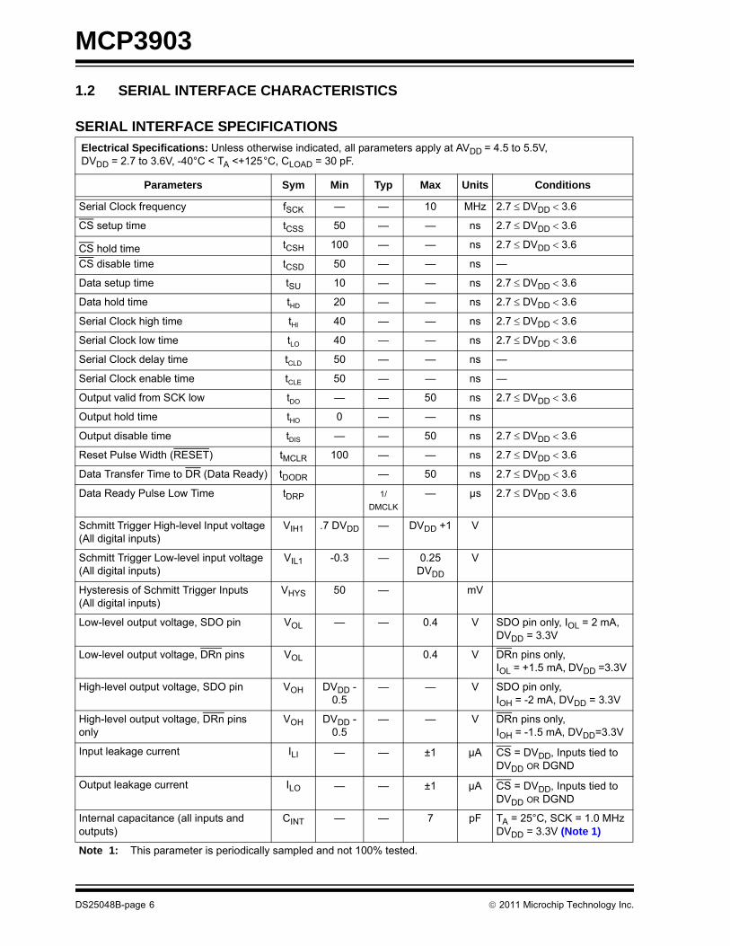
1.2 SERIAL INTERFACE CHARACTERISTICS
SERIAL INTERFACE SPECIFICATIONSElectrical Specifications: Unless otherwise indicated, all parameters apply at AVDD = 4.5 to 5.5V,DVDD = 2.7 to 3.6V, -40°C < TA <+125°C, CLOAD = 30 pF.
Parameters Sym Min Typ Max Units Conditions
Serial Clock frequency fSCK — — 10 MHz 2.7 ≤ DVDD < 3.6
CS setup time tCSS 50 — — ns 2.7 ≤ DVDD < 3.6
CS hold time tCSH 100 — — ns 2.7 ≤ DVDD < 3.6
CS disable time tCSD 50 — — ns —
Data setup time tSU 10 — — ns 2.7 ≤ DVDD < 3.6
Data hold time tHD 20 — — ns 2.7 ≤ DVDD < 3.6
Serial Clock high time tHI 40 — — ns 2.7 ≤ DVDD < 3.6
Serial Clock low time tLO 40 — — ns 2.7 ≤ DVDD < 3.6
Serial Clock delay time tCLD 50 — — ns —
Serial Clock enable time tCLE 50 — — ns —
Output valid from SCK low tDO — — 50 ns 2.7 ≤ DVDD < 3.6
Output hold time tHO 0 — — ns
Output disable time tDIS — — 50 ns 2.7 ≤ DVDD < 3.6
Reset Pulse Width (RESET) tMCLR 100 — — ns 2.7 ≤ DVDD < 3.6
Data Transfer Time to DR (Data Ready) tDODR — 50 ns 2.7 ≤ DVDD < 3.6
Data Ready Pulse Low Time tDRP 1/DMCLK
— µs 2.7 ≤ DVDD < 3.6
Schmitt Trigger High-level Input voltage (All digital inputs)
VIH1 .7 DVDD — DVDD +1 V
Schmitt Trigger Low-level input voltage (All digital inputs)
VIL1 -0.3 — 0.25 DVDD
V
Hysteresis of Schmitt Trigger Inputs(All digital inputs)
VHYS 50 — mV
Low-level output voltage, SDO pin VOL — — 0.4 V SDO pin only, IOL = 2 mA, DVDD = 3.3V
Low-level output voltage, DRn pins VOL 0.4 V DRn pins only,IOL = +1.5 mA, DVDD =3.3V
High-level output voltage, SDO pin VOH DVDD -0.5
— — V SDO pin only, IOH = -2 mA, DVDD = 3.3V
High-level output voltage, DRn pins only
VOH DVDD -0.5
— — V DRn pins only, IOH = -1.5 mA, DVDD=3.3V
Input leakage current ILI — — ±1 µA CS = DVDD, Inputs tied to DVDD OR DGND
Output leakage current ILO — — ±1 µA CS = DVDD, Inputs tied to DVDD OR DGND
Internal capacitance (all inputs and outputs)
CINT — — 7 pF TA = 25°C, SCK = 1.0 MHz DVDD = 3.3V (Note 1)
Note 1: This parameter is periodically sampled and not 100% tested.
DS25048B-page 6 © 2011 Microchip Technology Inc.

MCP3903
FIGURE 1-1: Serial Output Timing Diagram.
FIGURE 1-2: Serial Input Timing Diagram.
TEMPERATURE CHARACTERISTICSElectrical Specifications: Unless otherwise indicated, all parameters apply at AVDD = 4.5 to 5.5V, DVDD = 2.7 to 3.3 V.
Parameters Sym Min Typ Max Units Conditions
Temperature Ranges
Operating Temperature Range TA -40 — +125 °C (Note 1)Storage Temperature Range TA -65 — +150 °C
Thermal Package Resistances
Thermal Resistance, 28-lead SSOP
θJA — 71 — °C/W
Note 1: The internal junction temperature (TJ) must not exceed the absolute maximum specification of +150°C.
tCSH
tDIS
tHI tLO
fSCK
CS
SCK
SDO MSB out LSB out
Don’t CareSDI
Mode 1,1Mode 0,0
tHOtDO
CS
SCK
SDI LSB inMSB in
Mode 1,1Mode 0,0
tCSS
tSU tHD
tCSD
tCSHtCLD
tCLE
SDOHI-Z
tHI tLO
fSCK
© 2011 Microchip Technology Inc. DS25048B-page 7

MCP3903
HFIGURE 1-3: Data Ready Pulse Timing Diagram.H
FIGURE 1-4: Specific Timing Diagrams.
FIGURE 1-5: MCP3903 Clock Detail.
DR
SCK
SDO
1 / DRCLK
tDODRtDRP
CS VIH
Timing Waveform for tDIS
HI-Z
90%
10%
tDISSDO
SCK
SDO
tDO
Timing Waveform for tDO
MDAT0/1
OSC1/CLKI
Timing Waveform for MDAT0/1Modulator Output
tDOMDAT
CLKEXT
1
0
PRESCALE<1:0>
1 /
MCLK AMCLK1 / 4
DMCLK1 / OSR
DRCLK
OSR<1:0>
Multiplexer Clock Divider Clock Divider Clock DividerCrystalOscillator
OSC1
OSC2
Prescale
fS ADCSamplingRate
fD ADCOutputData Rate
Digital Buffer
DS25048B-page 8 © 2011 Microchip Technology Inc.

MCP3903
2.0 TYPICAL PERFORMANCE CURVES
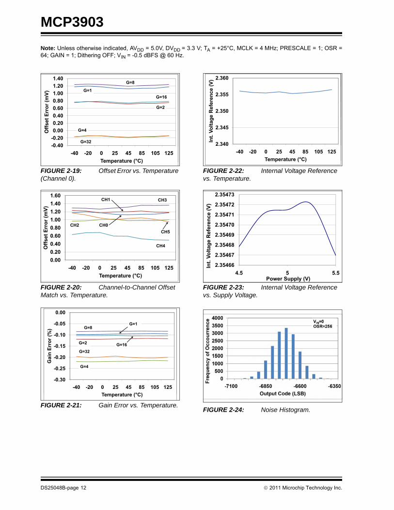
Note: Unless otherwise indicated, AVDD = 5.0V, DVDD = 3.3 V; Internal VREF; TA = +25°C, MCLK = 4 MHz; PRESCALE= 1; OSR = 64; GAIN = 1; Dithering OFF; VIN = -0.5 dBFS @ 60 Hz..
FIGURE 2-1: Spectral Response.
FIGURE 2-2: Spectral Response.
FIGURE 2-3: Spectral Response.
FIGURE 2-4: Spectral Response.
FIGURE 2-5: Spectral Response.
FIGURE 2-6: Spectral Response.
Note: The graphs and tables provided following this note are a statistical summary based on a limited number ofsamples and are provided for informational purposes only. The performance characteristics listed hereinare not tested or guaranteed. In some graphs or tables, the data presented may be outside the specifiedoperating range (e.g., outside specified power supply range) and therefore outside the warranted range.
© 2011 Microchip Technology Inc. DS25048B-page 9

MCP3903
Note: Unless otherwise indicated, AVDD = 5.0V, DVDD = 3.3 V; TA = +25°C, MCLK = 4 MHz; PRESCALE = 1; OSR =64; GAIN = 1; Dithering OFF; VIN = -0.5 dBFS @ 60 Hz..FIGURE 2-7: Spectral Response.
FIGURE 2-8: Spurious Free Dynamic Range vs Oversampling Ratio.
FIGURE 2-9: Signal-to-Noise and Distortion vs. Oversampling Ratio.
FIGURE 2-10: Signal-to-Noise and Distortion vs. Gain (Dithering OFF).
FIGURE 2-11: Signal-to-Noise and Distortion vs. Gain (Dithering ON).
FIGURE 2-12: Total Harmonic Distortion vs. Oversampling Ratio.
120
ic Dithering ON
80
100
120
Dyn
am
icB
)
Dithering ON
Dithering OFF
60
80
100
120
Fre
e D
yn
am
ic
ng
e (
dB
)
Dithering ON
Dithering OFF
40
60
80
100
120
rio
us F
ree D
yn
am
ic
Ran
ge (
dB
)
Dithering ON
Dithering OFF
0
20
40
60
80
100
120
Sp
uri
ou
s F
ree D
yn
am
ic
Ran
ge (
dB
)
Dithering ON
Dithering OFF
0
20
40
60
80
100
120
32 64 128 256
Sp
uri
ou
s F
ree D
yn
am
ic
Ran
ge (
dB
)
Oversampling Ratio (OSR)
Dithering ON
Dithering OFF
0
20
40
60
80
100
120
32 64 128 256
Sp
uri
ou
s F
ree D
yn
am
ic
Ran
ge (
dB
)
Oversampling Ratio (OSR)
Dithering ON
Dithering OFF
120
80
100
120
B) Dithering OFF
Dithering ON
60
80
100
120
NA
D (
dB
) Dithering OFF
Dithering ON
40
60
80
100
120
SIN
AD
(d
B) Dithering OFF
Dithering ON
0
20
40
60
80
100
120
SIN
AD
(d
B) Dithering OFF
Dithering ON
0
20
40
60
80
100
120
32 64 128 256
SIN
AD
(d
B)
Oversampling Ratio (OSR)
Dithering OFF
Dithering ON
0
20
40
60
80
100
120
32 64 128 256
SIN
AD
(d
B)
Oversampling Ratio (OSR)
Dithering OFF
Dithering ON
95
100
85
90
95
100
B) OSR = 256
70
75
80
85
90
95
100
NA
D (
dB
) OSR = 256
OSR = 128OSR = 64
60
65
70
75
80
85
90
95
100
SIN
AD
(d
B) OSR = 256
OSR = 128
OSR = 32
OSR = 64
50
55
60
65
70
75
80
85
90
95
100
SIN
AD
(d
B) OSR = 256
OSR = 128
OSR = 32
OSR = 64
50
55
60
65
70
75
80
85
90
95
100
1 2 4 8 16 32
SIN
AD
(d
B)
GAIN (V/V)
OSR = 256
OSR = 128
OSR = 32
OSR = 64
50
55
60
65
70
75
80
85
90
95
100
1 2 4 8 16 32
SIN
AD
(d
B)
GAIN (V/V)
OSR = 256
OSR = 128
OSR = 32
OSR = 64
95
100
85
90
95
100
)
OSR = 256
75
80
85
90
95
100
AD
(d
B)
OSR = 256
OSR = 128
65
70
75
80
85
90
95
100
SIN
AD
(d
B)
OSR = 256
OSR = 128
OSR = 64
55
60
65
70
75
80
85
90
95
100
SIN
AD
(d
B)
OSR = 256
OSR = 128
OSR = 64
OSR = 32
50
55
60
65
70
75
80
85
90
95
100
1 2 4 8 16 32
SIN
AD
(d
B)
OSR = 256
OSR = 128
OSR = 64
OSR = 32
50
55
60
65
70
75
80
85
90
95
100
1 2 4 8 16 32
SIN
AD
(d
B)
GAIN (V/V)
OSR = 256
OSR = 128
OSR = 64
OSR = 32
DS25048B-page 10 © 2011 Microchip Technology Inc.

MCP3903
Note: Unless otherwise indicated, AVDD = 5.0V, DVDD = 3.3 V; TA = +25°C, MCLK = 4 MHz; PRESCALE = 1; OSR =64; GAIN = 1; Dithering OFF; VIN = -0.5 dBFS @ 60 Hz..FIGURE 2-13: Total Harmonic Distortion vs. Input Signal Frequency.
FIGURE 2-14: Total Harmonic Distortion vs. Temperature.
FIGURE 2-15: Signal-to-Noise and Distortion vs. Input Signal Frequency.
FIGURE 2-16: Signal-to-Noise and Distortion vs. Temperature.
FIGURE 2-17: Signal-to-Noise and Distortion vs. Input Signal Amplitude.
FIGURE 2-18: Signal-to-Noise and Distortion vs. Master Clock.
-60
on fs=15.625KHz
OSR 64
80
-70
-60
sto
rtio
n fs=15.625KHzOSR=64
-90
-80
-70
-60
on
ic D
isto
rtio
n
dB
c)
fs=15.625KHzOSR=64
Dithering OFF
-100
-90
-80
-70
-60
Harm
on
ic D
isto
rtio
n
(dB
c)
fs=15.625KHzOSR=64
Dithering OFF
Dithering ON
-110
-100
-90
-80
-70
-60
To
tal
Harm
on
ic D
isto
rtio
n
(dB
c)
fs=15.625KHzOSR=64
Dithering OFF
Dithering ON
-120
-110
-100
-90
-80
-70
-60
20 50 100 200 500 1000 2000
To
tal
Harm
on
ic D
isto
rtio
n
(dB
c)
fs=15.625KHzOSR=64
Dithering OFF
Dithering ON
-120
-110
-100
-90
-80
-70
-60
20 50 100 200 500 1000 2000
To
tal
Harm
on
ic D
isto
rtio
n
(dB
c)
Input Frequency (Hz)
fs=15.625KHzOSR=64
Dithering OFF
Dithering ON
0
on fs=15.625KHz
-40
-20
0
Dis
tort
ion fs=15.625KHz
OSR=64
-60
-40
-20
0
mo
nic
Dis
tort
ion
(d
Bc)
fs=15.625KHzOSR=64
-80
-60
-40
-20
0
Harm
on
ic D
isto
rtio
n
(dB
c)
fs=15.625KHzOSR=64
-120
-100
-80
-60
-40
-20
0
To
tal
Harm
on
ic D
isto
rtio
n
(dB
c)
fs=15.625KHzOSR=64
-120
-100
-80
-60
-40
-20
0
-40 -20 0 25 45 85 105 125
To
tal
Harm
on
ic D
isto
rtio
n
(dB
c)
Temperature (°C)
fs=15.625KHzOSR=64
-120
-100
-80
-60
-40
-20
0
-40 -20 0 25 45 85 105 125
To
tal
Harm
on
ic D
isto
rtio
n
(dB
c)
Temperature (°C)
fs=15.625KHzOSR=64
90
100
Dithering OFF
70
80
90
100
B)
Dithering OFF
Dithering ON
40
50
60
70
80
90
100
NA
D (
dB
)
Dithering OFF
Dithering ON
20
30
40
50
60
70
80
90
100
SIN
AD
(d
B)
Dithering OFF
Dithering ON
fs=15 625KHz
0
10
20
30
40
50
60
70
80
90
100
SIN
AD
(d
B)
Dithering OFF
Dithering ON
fs=15.625KHzOSR=64
0
10
20
30
40
50
60
70
80
90
100
20 50 100 200 500 1000 2000
SIN
AD
(d
B)
Input Frequency (Hz)
Dithering OFF
Dithering ON
fs=15.625KHzOSR=64
0
10
20
30
40
50
60
70
80
90
100
20 50 100 200 500 1000 2000
SIN
AD
(d
B)
Input Frequency (Hz)
Dithering OFF
Dithering ON
fs=15.625KHzOSR=64
120fs=15.625KHz
80
100
120
)
fs=15.625KHzOSR=64
60
80
100
120
AD
(d
B)
fs=15.625KHzOSR=64
40
60
80
100
120
SIN
AD
(d
B)
fs=15.625KHzOSR=64
20
40
60
80
100
120
SIN
AD
(d
B)
fs=15.625KHzOSR=64
0
20
40
60
80
100
120
-40 -20 0 25 45 85 105 125
SIN
AD
(d
B)
fs=15.625KHzOSR=64
0
20
40
60
80
100
120
-40 -20 0 25 45 85 105 125
SIN
AD
(d
B)
Temperature (°C)
fs=15.625KHzOSR=64
80
90
60
70
80
90
B)
40
50
60
70
80
90
NA
D (
dB
)
20
30
40
50
60
70
80
90
SIN
AD
(d
B)
0
10
20
30
40
50
60
70
80
90
SIN
AD
(d
B)
-10
0
10
20
30
40
50
60
70
80
90
0.00001 0.001 0.1 10 1000
SIN
AD
(d
B)
Input Signal Amplitude (mV)
-10
0
10
20
30
40
50
60
70
80
90
0.00001 0.001 0.1 10 1000
SIN
AD
(d
B)
Input Signal Amplitude (mV)
© 2011 Microchip Technology Inc. DS25048B-page 11
MCP3903
Note: Unless otherwise indicated, AVDD = 5.0V, DVDD = 3.3 V; TA = +25°C, MCLK = 4 MHz; PRESCALE = 1; OSR =64; GAIN = 1; Dithering OFF; VIN = -0.5 dBFS @ 60 Hz.FIGURE 2-19: Offset Error vs. Temperature (Channel 0).
FIGURE 2-20: Channel-to-Channel Offset Match vs. Temperature.
FIGURE 2-21: Gain Error vs. Temperature.
FIGURE 2-22: Internal Voltage Reference vs. Temperature.
FIGURE 2-23: Internal Voltage Reference vs. Supply Voltage.
FIGURE 2-24: Noise Histogram.
1 20
1.40G=8
0.80
1.00
1.20
1.40
(mV
)
G=16
G=1
G=8
0.40
0.60
0.80
1.00
1.20
1.40
Err
or
(mV
)
G=2
G=16
G=1
G=8
0 00
0.20
0.40
0.60
0.80
1.00
1.20
1.40
Off
se
t E
rro
r (m
V)
G=4
G=2
G=16
G=1
G=8
-0.40
-0.20
0.00
0.20
0.40
0.60
0.80
1.00
1.20
1.40
Off
se
t E
rro
r (m
V)
G=32
G=4
G=2
G=16
G=1
G=8
-0.40
-0.20
0.00
0.20
0.40
0.60
0.80
1.00
1.20
1.40
-40 -20 0 25 45 85 105 125
Off
se
t E
rro
r (m
V)
Temperature (°C)
G=32
G=4
G=2
G=16
G=1
G=8
-0.40
-0.20
0.00
0.20
0.40
0.60
0.80
1.00
1.20
1.40
-40 -20 0 25 45 85 105 125
Off
se
t E
rro
r (m
V)
Temperature (°C)
G=32
G=4
G=2
G=16
G=1
G=8
1 40
1.60CH1 CH3
1 00
1.20
1.40
1.60
r (m
V)
CH1 CH3
0 60
0.80
1.00
1.20
1.40
1.60
t E
rro
r (m
V)
CH0
CH1
CH2
CH3
CH5
0.40
0.60
0.80
1.00
1.20
1.40
1.60
Off
se
t E
rro
r (m
V)
CH0
CH1
CH2
CH3
CH4
CH5
0.00
0.20
0.40
0.60
0.80
1.00
1.20
1.40
1.60
Off
se
t E
rro
r (m
V)
CH0
CH1
CH2
CH3
CH4
CH5
0.00
0.20
0.40
0.60
0.80
1.00
1.20
1.40
1.60
-40 -20 0 25 45 85 105 125
Off
se
t E
rro
r (m
V)
Temperature (°C)
CH0
CH1
CH2
CH3
CH4
CH5
0.00
0.20
0.40
0.60
0.80
1.00
1.20
1.40
1.60
-40 -20 0 25 45 85 105 125
Off
se
t E
rro
r (m
V)
Temperature (°C)
CH0
CH1
CH2
CH3
CH4
CH5
0.00
-0.10
-0.05
0.00
(%)
G=1G=8
-0.15
-0.10
-0.05
0.00
Err
or
(%)
G=32
G=16G=2
G=1G=8
-0.20
-0.15
-0.10
-0.05
0.00
Ga
in E
rro
r (%
)
G=32
G=16G=2
G=1G=8
0 30
-0.25
-0.20
-0.15
-0.10
-0.05
0.00
Ga
in E
rro
r (%
)
G=32
G=4
G=16G=2
G=1G=8
-0.30
-0.25
-0.20
-0.15
-0.10
-0.05
0.00
-40 -20 0 25 45 85 105 125
Ga
in E
rro
r (%
)
Temperature (°C)
G=32
G=4
G=16G=2
G=1G=8
-0.30
-0.25
-0.20
-0.15
-0.10
-0.05
0.00
-40 -20 0 25 45 85 105 125
Ga
in E
rro
r (%
)
Temperature (°C)
G=32
G=4
G=16G=2
G=1G=8
2.360
(V)
2.355
2.360
ren
ce (
V)
2.350
2.355
2.360
e R
efe
ren
ce (
V)
2.345
2.350
2.355
2.360
Vo
ltag
e R
efe
ren
ce (
V)
2.340
2.345
2.350
2.355
2.360
Int.
Vo
ltag
e R
efe
ren
ce (
V)
2.340
2.345
2.350
2.355
2.360
-40 -20 0 25 45 85 105 125
Int.
Vo
ltag
e R
efe
ren
ce (
V)
Temperature (°C)
2.340
2.345
2.350
2.355
2.360
-40 -20 0 25 45 85 105 125
Int.
Vo
ltag
e R
efe
ren
ce (
V)
Temperature (°C)
2 35472
2.35473
2.35471
2.35472
2.35473
nce (
V)
2 35469
2.35470
2.35471
2.35472
2.35473
Refe
ren
ce (
V)
2.35468
2.35469
2.35470
2.35471
2.35472
2.35473
ag
e R
efe
ren
ce (
V)
2 35466
2.35467
2.35468
2.35469
2.35470
2.35471
2.35472
2.35473
nt.
Vo
ltag
e R
efe
ren
ce (
V)
2.35466
2.35467
2.35468
2.35469
2.35470
2.35471
2.35472
2.35473
4.5 5 5.5
Int.
Vo
ltag
e R
efe
ren
ce (
V)
Power Supply (V)
2.35466
2.35467
2.35468
2.35469
2.35470
2.35471
2.35472
2.35473
4.5 5 5.5
Int.
Vo
ltag
e R
efe
ren
ce (
V)
Power Supply (V)
DS25048B-page 12 © 2011 Microchip Technology Inc.

MCP3903
Note: Unless otherwise indicated, AVDD = 5.0V, DVDD = 3.3 V; TA = +25°C, MCLK = 4 MHz; PRESCALE = 1; OSR =64; GAIN = 1; Dithering OFF; VIN = -0.5 dBFS @ 60 Hz.FIGURE 2-25: Integral Non-Linearity (Dithering OFF).
FIGURE 2-26: Integral Non-Linearity (Dithering ON).
FIGURE 2-27: Operating Current vs. Master Clock (MCLK).
40
50CH0
20
30
40
50
m)
CH0
10
0
10
20
30
40
50
L (
pp
m)
CH0
CH1
30
-20
-10
0
10
20
30
40
50
INL
(p
pm
)
CH0
CH1
-50
-40
-30
-20
-10
0
10
20
30
40
50
INL
(p
pm
)
CH0
CH1
-50
-40
-30
-20
-10
0
10
20
30
40
50
-0.5 -0.25 0 0.25 0.5
INL
(p
pm
)
Input Voltage (V)
CH0
CH1
-50
-40
-30
-20
-10
0
10
20
30
40
50
-0.5 -0.25 0 0.25 0.5
INL
(p
pm
)
Input Voltage (V)
CH0
CH1
40
50
20
30
40
50
CH0
10
0
10
20
30
40
50
(pp
m)
CH0
CH1
30
-20
-10
0
10
20
30
40
50
INL
(p
pm
)
CH0
CH1
-50
-40
-30
-20
-10
0
10
20
30
40
50
INL
(p
pm
)
CH0
CH1
-50
-40
-30
-20
-10
0
10
20
30
40
50
-0.5 -0.25 0 0.25 0.5
INL
(p
pm
)
Input Voltage (V)
CH0
CH1
-50
-40
-30
-20
-10
0
10
20
30
40
50
-0.5 -0.25 0 0.25 0.5
INL
(p
pm
)
Input Voltage (V)
CH0
CH1
8
9
6
7
8
9
)
AIDD Boost OFF
4
5
6
7
8
9
D (
mA
)
AIDD Boost OFF
2
3
4
5
6
7
8
9
IDD
(m
A)
AIDD Boost OFF
0
1
2
3
4
5
6
7
8
9
IDD
(m
A)
AIDD Boost OFF
DIDD
0
1
2
3
4
5
6
7
8
9
1 2 3 4
IDD
(m
A)
MCLK Frequency(MHz)
AIDD Boost OFF
DIDD
0
1
2
3
4
5
6
7
8
9
1 2 3 4
IDD
(m
A)
MCLK Frequency(MHz)
AIDD Boost OFF
DIDD
© 2011 Microchip Technology Inc. DS25048B-page 13

MCP3903
3.0 PIN DESCRIPTIONTABLE 3-1: PIN FUNCTION TABLE
3.1 RESETThis pin is active low and places the entire chip in areset state when active.
When RESET=0, all registers are reset to their defaultvalue, no communication can take place, no clock isdistributed inside the part. This state is equivalent to aPOR state.
Since the default state of the ADCs is on, the analogpower consumption when RESET = 0 is equivalent towhen RESET = 1. Only the digital power consumptionis largely reduced because this current consumption isessentially dynamic and is reduced drastically whenthere is no clock running. All the analog biases are
enabled during a reset so that the part is fullyoperational just after a RESET rising edge. This inputis Schmitt triggered.
3.2 Digital VDD (DVDD)DVDD is the power supply pin for the digital circuitrywithin the MCP3903. This pin requires appropriatebypass capacitors and should be maintained between2.7V and 3.6V for specified operation.
Pin No. Symbol Function
1 AVDD Analog Power Supply Pin
2 CH0+ Non-Inverting Analog Input Pin for Channel 0
3 CH0- Inverting Analog Input Pin for Channel 0
4 CH1- Inverting Analog Input Pin for Channel 1
5 CH1+ Non-Inverting Analog Input Pin for Channel 1
6 CH2+ Non-Inverting Analog Input Pin for Channel 2
7 CH2- Inverting Analog Input Pin for Channel 2
8 CH3- Inverting Analog Input Pin for Channel 3
9 CH3+ Non-Inverting Analog Input Pin for Channel 3
10 CH4+ Non-Inverting Analog Input Pin for Channel 4
11 CH4- Inverting Analog Input Pin for Channel 4
12 CH5- Inverting Analog Input Pin for Channel 5
13 CH5+ Non-Inverting Analog Input Pin for Channel 5
14 REFIN+/OUT Non-Inverting Voltage Reference Input and Internal Reference Output Pin
15 REFIN- Inverting Voltage Reference Input Pin
16 AGND Analog Ground Pin, Return Path for internal analog circuitry
17 DGND Digital Ground Pin, Return Path for internal digital circuitry
18 DRA Data Ready Signal Output for channels pair A
19 DRB Data Ready Signal Output for channels pair B
20 DRC Data Ready Signal Output for channels pair C
21 OSC1 Oscillator Crystal Connection Pin or Clock Input Pin
22 OSC2 Oscillator Crystal Connection Pin
23 CS Chip Select for Serial Interface
24 SCK Serial Interface Clock Pin
25 SDO Serial Interface Data Output Pin
26 SDI Serial Interface Data Input Pin
27 RESET Master Reset Logic Input Pin
28 DVDD Digital Power Supply Pin
DS25048B-page 14 © 2011 Microchip Technology Inc.

MCP3903
3.3 Analog VDD (AVDD)AVDD is the power supply pin for the analog circuitrywithin the MCP3903.This pin requires appropriate bypass capacitors andshould be maintained to 5V ±10% for specifiedoperation.
3.4 ADC Differential Analog Inputs(CHn+/CHn-)
CHn- and CHn+, are the two fully-differential analogvoltage inputs for the Delta-Sigma ADCs. There are sixchannels in total grouped in three channel pairs.
The linear and specified region of the channels aredependent on the PGA gain. This region correspondsto a differential voltage range of ±500 mV/GAIN withVREF = 2.4V. The maximum absolute voltage, withrespect to AGND, for each CHn+/- input pin is +/-1Vwith no distortion and ±6V with no breaking aftercontinuous voltage.
3.5 Analog Ground (AGND)AGND is the ground connection to internal analogcircuitry (ADCs, PGA, voltage reference, POR). Toensure accuracy and noise cancellation, this pin mustbe connected to the same ground as DGND, preferablywith a star connection. If an analog ground plane isavailable, it is recommended that this pin be tied to thisplane of the PCB. This plane should also reference allother analog circuitry in the system.
3.6 Non-Inverting Reference Input, Internal Reference Output (REFIN+/OUT)
This pin is the non-inverting side of the differentialvoltage reference input for all ADCs or the internalvoltage reference output. When VREFEXT = 1, and anexternal voltage reference source can be used, theinternal voltage reference is disabled. When using anexternal differential voltage reference, it should beconnected to its VREF+ pin.
When using an external single-ended reference, itshould be connected to this pin.
When VREFEXT = 0, the internal voltage reference isenabled and connected to this pin through a switch.This voltage reference has minimal drive capability andthus needs proper buffering and bypass capacitances(10 μF tantalum in parallel with 0.1 μF ceramic) if usedas a voltage source.
For optimal performance, bypass capacitances shouldbe connected between this pin and AGND at all timeseven when the internal voltage reference is used.
3.7 Inverting Reference Input (REFIN-)This pin is the inverting side of the differential voltagereference input for both ADCs. When using an externaldifferential voltage reference, it should be connected toits VREF- pin. When using an external single-endedvoltage reference, or when VREFEXT = 0 (Default)and using the internal voltage reference, this pin shouldbe directly connected to AGND.
3.8 Digital Ground Connection (DGND)
DGND is the ground connection to internal digitalcircuitry (SINC filters, oscillator, serial interface). Toensure accuracy and noise cancellation, DGND mustbe connected to the same ground as AGND, preferablywith a star connection. If a digital ground plane isavailable, it is recommended that this pin be tied to thisplane of the Printed Circuit Board (PCB). This planeshould also reference all other digital circuitry in thesystem.
3.9 DRn (Data Ready Pins)The Data Ready pins indicate if a new conversionresult is ready to be read on each of the A, B and Cpairs of ADCs. The default state of this pin is high whenDR_HIZN=1 and is high impedance when DR_HIZN=0(Default). After each conversion is finished, a low pulsewill take place on the data ready pins to indicate theconversion result is ready as an interrupt. This pulse issynchronous with the master clock and has a definedand constant width.
The Data Ready pins are independent of the SPIinterface and act like an interrupt output.The DataReady pins state is not latched and the pulse width(and period) are both determined by the MCLKfrequency, over-sampling rate, and internal clock pre-scale settings. The DR pulse width is equal to oneDMCLK period and the frequency of the pulses is equalto DRCLK (see Figure 1-3).
Note: These pins should not be left floatingwhen DR_HIZ bit is low; a 100kΩ pull-upresistor connected to DVDD is recom-mended.
© 2011 Microchip Technology Inc. DS25048B-page 15

MCP3903
3.10 Oscillator And Master Clock InputPins (OSC1/CLKI, OSC2)OSC1/CLKI and OSC2 provide the master clock for thedevice. When CLKEXT = 0 (Default), a resonantcrystal or clock source with a similar sinusoidalwaveform must be placed across these pins to ensureproper operation. The typical clock frequency specifiedis 4 MHz. However, the clock frequency can be 1 MHzto 5 MHz without disturbing ADC accuracy. With thecurrent boost circuit enabled, the master clock can beused up to 8.192 MHz without disturbing ADCaccuracy. Appropriate load capacitance should beconnected to these pins for proper operation.
3.11 CS (Chip Select)This pin is the SPI Chip Select that enables the serialcommunication. When this pin is high, nocommunication can take place. A chip select fallingedge initiates the serial communication and a chipselect rising edge terminates the communication. Nocommunication can take place even when CS is lowand when RESET is low.
This input is Schmitt-triggered.
3.12 SCK (Serial Data Clock)This is the serial clock pin for SPI communication. Datais clocked into the device on the RISING edge of SCK.Data is clocked out of the device on the FALLING edgeof SCK. The MCP3903 interface is compatible withboth SPI 0,0 and 1,1 modes. The maximum clockspeed specified is 10 MHz. This input is Schmitttriggered.
3.13 SDO (Serial Data Output)This is the SPI data output pin. Data is clocked out ofthe device on the FALLING edge of SCK. This pin staysat high impedance during the control byte. It also staysat high impedance during the whole communication forwrite commands and when the CS pin is high or whenthe RESET pin is low. This pin is active only when aread command is processed. Each read is processedby a packet of 24 bits (size of each register), except onthe ADC output registers when WIDTH=0.
3.14 SDI (Serial Data Input)This is the SPI data input pin. Data is clocked into thedevice on the RISING edge of SCK. When CS is low,this pin is used to communicate with a series of 8-bitcommands. The interface is half-duplex (inputs andoutputs do not happen at the same time). Eachcommunication starts with a chip select falling edgefollowed by an 8-bit control byte entered through theSDI pin. Each write is processed by packets of 24 bits(size of each register). Each command is either a Reador a Write command. Toggling SDI during a Readcommand has no effect. This input is Schmitt-triggered.
Note: When CLKEXT = 1, the crystal oscillatoris disabled, as well as the OSC2 input.The OSC1 becomes the master clockinput CLKI, direct path for an externalclock source, for example a clock sourcegenerated by an MCU.
DS25048B-page 16 © 2011 Microchip Technology Inc.
MCP3903
4.0 TERMINOLOGY AND FORMULAS
This section defines the terms and formulas usedthroughout this data sheet. The following terms aredefined:
MCLK - Master Clock
AMCLK - Analog Master Clock
DMCLK - Digital Master Clock
DRCLK - Data Rate Clock
OSR - Oversampling Ratio
Offset Error
Gain Error
Integral Non-Linearity Error
Signal-To-Noise Ratio (SNR)
Signal-To-Noise Ratio And Distortion (SINAD)
Total Harmonic Distortion (THD)
Spurious-Free Dynamic Range (SFDR)
MCP3903 Delta-Sigma Architecture
Idle Tones
Dithering
Crosstalk
PSRR
CMRR
ADC Reset Mode
Hard Reset Mode (RESET = 0)
ADC Shutdown Mode
Full Shutdown Mode
4.1 MCLK - Master ClockThis is the fastest clock present in the device. This isthe frequency of the crystal placed at the OSC1/OSC2inputs when CLKEXT = 0 or the frequency of the clockinput at the OSC1/CLKI when CLKEXT = 1.
4.2 AMCLK - Analog Master ClockThis is the clock frequency that is present on the analogportion of the device, after prescaling has occurred viathe CONFIG PRESCALE<1:0> register bits. Theanalog portion includes the PGAs and the twosigma-delta modulators.
EQUATION 4-1:
4.3 DMCLK - Digital Master ClockThis is the clock frequency that is present on the digitalportion of the device, after prescaling and division by 4.This is also the sampling frequency, that is the rate atwhich the modulator outputs are refreshed. Eachperiod of this clock corresponds to one sample and onemodulator output.
EQUATION 4-2:
4.4 DRCLK - Data Rate ClockThis is the output data rate i.e. the rate at which theADCs output new data. Each new data is signaled by adata ready pulse on the DR pin.
This data rate is depending on the OSR and theprescaler with the following formula:
EQUATION 4-3:
TABLE 4-1: MCP3903 OVERSAMPLING RATIO SETTINGS
Config Analog Master Clock Prescale PRE<1:0>
0 0 AMCLK = MCLK/ 1 (default)0 1 AMCLK = MCLK/ 21 0 AMCLK = MCLK/ 41 1 AMCLK = MCLK/ 8
AMCLK MCLKPRESCALE-------------------------------=
DMCLK AMCLK4--------------------- MCLK
4 PRESCALE×----------------------------------------= =
DRCLK DMCLKOSR
---------------------- AMCLK4 OSR×--------------------- MCLK
4 OSR PRESCALE××-----------------------------------------------------------= = =
© 2011 Microchip Technology Inc. DS25048B-page 17

MCP3903
Since this is the output data rate, and since thedecimation filter is a SINC (or notch) filter, there is anotch in the filter transfer function at each integermultiple of this rate.The following table describes the various combinationsof OSR and PRESCALE and their associated AMCLK,DMCLK and DRCLK rates.
4.5 OSR - Oversampling RatioThe ratio of the sampling frequency to the output datarate is OSR = DMCLK/DRCLK. The default OSR is 64,or with MCLK = 4 MHz, PRESCALE = 1, AMCLK = 4MHz, fS = 1 MHz, fD = 15.625 ksps. The following bitsin the CONFIG1 register are used to change theoversampling ratio (OSR).
4.6 Offset ErrorThis is the error induced by the ADC when the inputsare shorted together (VIN = 0V). The specificationincorporates both PGA and ADC offset contributions.This error varies with PGA and OSR settings. Theoffset is different on each channel and varies from chipto chip. This offset error can easily be calibrated out bya MCU with a subtraction. The offset is specified in mV.
The offset on the MCP3903 has a low temperaturecoefficient, see Section 2.0 “Typical PerformanceCurves”.
4.7 Gain ErrorThis is the error induced by the ADC on the slope of thetransfer function. It is the deviation expressed in %compared to the ideal transfer function defined byEquation 5-3. The specification incorporates both PGAand ADC gain error contributions, but not the VREFcontribution (it is measured with an external VREF).Thiserror varies with PGA and OSR settings.
The gain error on the MCP3903 has a low temperaturecoefficient. See the typical performance curves formore information.
TABLE 4-2: DEVICE DATA RATES IN FUNCTION OF MCLK, OSR, AND PRESCALEPRE<1:0> OSR <1:0> OSR AMCLK DMCLK DRCLK DRCLK
(ksps)
1 1 1 1 256 MCLK/8 MCLK/32 MCLK/8192 0.48821 1 1 0 128 MCLK/8 MCLK/32 MCLK/4096 0.9761 1 0 1 64 MCLK/8 MCLK/32 MCLK/2048 1.951 1 0 0 32 MCLK/8 MCLK/32 MCLK/1024 3.91 0 1 1 256 MCLK/4 MCLK/16 MCLK/4096 0.9761 0 1 0 128 MCLK/4 MCLK/16 MCLK/2048 1.951 0 0 1 64 MCLK/4 MCLK/16 MCLK/1024 3.91 0 0 0 32 MCLK/4 MCLK/16 MCLK/512 7.81250 1 1 1 256 MCLK/2 MCLK/8 MCLK/2048 1.950 1 1 0 128 MCLK/2 MCLK/8 MCLK/1024 3.90 1 0 1 64 MCLK/2 MCLK/8 MCLK/512 7.81250 1 0 0 32 MCLK/2 MCLK/8 MCLK/256 15.6250 0 1 1 256 MCLK MCLK/4 MCLK/1024 3.90 0 1 0 128 MCLK MCLK/4 MCLK/512 7.81250 0 0 1 64 MCLK MCLK/4 MCLK/256 15.6250 0 0 0 32 MCLK MCLK/4 MCLK/128 31.25
Note: For OSR = 32 and 64, DITHER = 0. For OSR = 128 and 256, DITHER = 1.
TABLE 4-3: MCP3903 OVERSAMPLING RATIO SETTINGS
CONFIG OVER SAMPLING RATIO(OSR)
OSR<1:0>
0 0 320 1 64 (DEFAULT)1 0 128 1 1 256
DS25048B-page 18 © 2011 Microchip Technology Inc.

MCP3903
4.8 Integral Non-Linearity ErrorIntegral non-linearity error is the maximum deviation ofan ADC transition point from the corresponding point ofan ideal transfer function, with the offset and gainerrors removed, or with the end points equal to zero.It is the maximum remaining error after calibration ofoffset and gain errors for a DC input signal.
4.9 Signal-To-Noise Ratio (SNR)For the MCP3903 ADC, the signal-to-noise ratio is aratio of the output fundamental signal power to thenoise power (not including the harmonics of the signal),when the input is a sinewave at a predeterminedfrequency. It is measured in dB. Usually, only themaximum signal to noise ratio is specified. The SNRfigure depends mainly on the OSR and DITHERsettings of the device.
EQUATION 4-4: SIGNAL-TO-NOISE RATIO
4.10 Signal-To-Noise Ratio And Distortion (SINAD)
The most important figure of merit for the analogperformance of the ADCs present on the MCP3903 isthe Signal-to-Noise And Distortion (SINAD)specification.
Signal-to-noise and distortion ratio is similar to signal-to-noise ratio, with the exception that you must includethe harmonics power in the noise power calculation.The SINAD specification depends mainly on the OSRand DITHER settings.
EQUATION 4-5: SINAD EQUATION
The calculated combination of SNR and THD per thefollowing formula also yields SINAD:
EQUATION 4-6: SINAD, THD, AND SNR RELATIONSHIP
4.11 Total Harmonic Distortion (THD)The total harmonic distortion is the ratio of the outputharmonics power to the fundamental signal power for asinewave input and is defined by the followingequation.
EQUATION 4-7:
The THD calculation includes the first 35 harmonics forthe MCP3903 specifications. The THD is usually onlymeasured with respect to the 10 first harmonics. THDis sometimes expressed in %. For converting the THDin %, here is the formula:
EQUATION 4-8:
This specification depends mainly on the DITHERsetting.
4.12 Spurious-Free Dynamic Range (SFDR)
SFDR is the ratio between the output power of thefundamental and the highest spur in the frequencyspectrum. The spur frequency is not necessarily aharmonic of the fundamental even though it is usuallythe case. This figure represents the dynamic range ofthe ADC when a full-scale signal is used at the input.This specification depends mainly on the DITHERsetting.
EQUATION 4-9:
SNR dB( ) 10 SignalPowerNoisePower----------------------------------⎝ ⎠
⎛ ⎞log=
SINAD dB( ) 10 SignalPowerNoise HarmonicsPower+--------------------------------------------------------------------⎝ ⎠
⎛ ⎞log=
SINAD dB( ) 10 10
SNR10-----------⎝ ⎠
⎛ ⎞
10
THD–10----------------⎝ ⎠
⎛ ⎞
+log=
THD dB( ) 10 HarmonicsPowerFundamentalPower-----------------------------------------------------⎝ ⎠
⎛ ⎞log=
THD %( ) 100 10THD dB( )
20------------------------×=
SFDR dB( ) 10 FundamentalPowerHighestSpurPower-----------------------------------------------------⎝ ⎠
⎛ ⎞log=
© 2011 Microchip Technology Inc. DS25048B-page 19

MCP3903
4.13 MCP3903 Delta-SigmaArchitectureThe MCP3903 incorporates six Delta-Sigma ADCs witha multi-bit digital to analog converter as quantizer. ADelta-Sigma ADC is an oversampling converter thatincorporates a built-in modulator which is digitizing thequantity of charge integrated by the modulator loop(see Figure 5-1). The quantizer is the block that is per-forming the analog-to-digital conversion. The quantizeris typically 1-bit, or a simple comparator which helps tomaintain the linearity performance of the ADC (theDAC structure is inherently linear in this case).
Multi-bit quantizers help to lower the quantization error(the error fed back in the loop can be very large with1-bit quantizers) without changing the order of themodulator or the OSR, which leads to better SNRfigures. However, typically, the linearity of sucharchitectures is more difficult to achieve since the DACis no more simple to realize and its linearity limits theTHD of such ADCs.
The MCP3903’s 5-level quantizer is a flash ADCcomposed of 4 comparators arranged with equallyspaced thresholds and a thermometer coding. TheMCP3903 also includes proprietary 5-level DACarchitecture that is inherently linear for improved THDfigures.
4.14 Idle TonesA Delta-Sigma converter is an integrating converter. Italso has a finite quantization step (LSB) which can bedetected by its quantizer. A DC input voltage that isbelow the quantization step should only provide an allzeros result since the input is not large enough to bedetected. As an integrating device, any Delta-Sigmawill show, in this case, idle tones. This means that theoutput will have spurs in the frequency content that aredepending on the ratio between quantization stepvoltage and the input voltage. These spurs are theresult of the integrated sub-quantization step inputsthat will eventually cross the quantization steps after along enough integration. This will induce an ACfrequency at the output of the ADC and can be shownin the ADC output spectrum.
These idle tones are residues that are inherent to thequantization process and the fact that the converter isintegrating at all times without being reset. They areresidues of the finite resolution of the conversionprocess. They are very difficult to attenuate and theyare heavily signal dependent. They can degrade bothSFDR and THD of the converter, even for DC inputs.They can be localized in the baseband of the converterand thus difficult to filter from the actual input signal.
For power metering applications, idle tones can be verydisturbing because energy can be detected even at the50 or 60 Hz frequency, depending on the DC offset ofthe ADCs, while no power is really present at theinputs. The only practical way to suppress or attenuateidle tones phenomenon is to apply dithering to theADC. The idle tones amplitudes are a function of theorder of the modulator, the OSR and the number oflevels in the quantizer of the modulator. A higher order,a higher OSR, or a higher number of levels for thequantizer will attenuate the idle tones amplitude.
4.15 DitheringIn order to suppress or attenuate the idle tones presentin any Delta-Sigma ADCs, dithering can be applied tothe ADC. Dithering is the process of adding an error tothe ADC feedback loop in order to “decorrelate” theoutputs and “break” the idle tone’s behavior. Usually arandom or pseudo-random generator adds an analogor digital error to the feedback loop of the delta-sigmaADC in order to ensure that no tonal behavior canhappen at its outputs. This error is filter by the feedbackloop and typically has a zero average value so that theconverter static transfer function is not disturbed by thedithering process. However, the dithering processslightly increases the noise floor (it adds noise to thepart) while reducing its tonal behavior and thusimproving SFDR and THD. The dithering processscrambles the idle tones into baseband white noise andensures that dynamic specs (SNR, SINAD, THD,SFDR) are less signal dependent. The MCP3903incorporates a proprietary dithering algorithm on allADCs in order to remove idle tones and improve THD,which is crucial for power metering applications.
DS25048B-page 20 © 2011 Microchip Technology Inc.
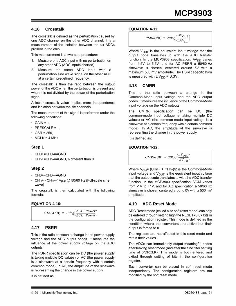
MCP3903
4.16 CrosstalkThe crosstalk is defined as the perturbation caused byone ADC channel on the other ADC channel. It is ameasurement of the isolation between the six ADCspresent in the chip.This measurement is a two-step procedure:
1. Measure one ADC input with no perturbation onany other ADC (ADC inputs shorted).
2. Measure the same ADC input with aperturbation sine wave signal on the other ADCat a certain predefined frequency.
The crosstalk is then the ratio between the outputpower of the ADC when the perturbation is present andwhen it is not divided by the power of the perturbationsignal.
A lower crosstalk value implies more independenceand isolation between the six channels.
The measurement of this signal is performed under thefollowing conditions:
• GAIN = 1,• PRESCALE = 1,• OSR = 256, • MCLK = 4 MHz
Step 1• CH0+=CH0-=AGND• CHn+=CHn-=AGND, n different than 0
Step 2• CH0+=CH0-=AGND• CHn+ - CHn-=1VP-P @ 50/60 Hz (Full-scale sine
wave)
The crosstalk is then calculated with the followingformula:
EQUATION 4-10:
4.17 PSRRThis is the ratio between a change in the power supplyvoltage and the ADC output codes. It measures theinfluence of the power supply voltage on the ADCoutputs.
The PSRR specification can be DC (the power supplyis taking multiple DC values) or AC (the power supplyis a sinewave at a certain frequency with a certaincommon mode). In AC, the amplitude of the sinewaveis representing the change in the power supply.
It is defined as:
EQUATION 4-11:
Where VOUT is the equivalent input voltage that theoutput code translates to with the ADC transferfunction. In the MCP3903 specification, AVDD variesfrom 4.5V to 5.5V, and for AC PSRR a 50/60 Hzsinewave is chosen, centered around 5V with amaximum 500 mV amplitude. The PSRR specificationis measured with DVDD = 3.3V.
4.18 CMRRThis is the ratio between a change in theCommon-Mode input voltage and the ADC outputcodes. It measures the influence of the Common-Modeinput voltage on the ADC outputs.
The CMRR specification can be DC (thecommon-mode input voltage is taking multiple DCvalues) or AC (the common-mode input voltage is asinewave at a certain frequency with a certain commonmode). In AC, the amplitude of the sinewave isrepresenting the change in the power supply.
It is defined as:
EQUATION 4-12:
Where VCM= (CHn+ + CHn-)/2 is the Common-Modeinput voltage and VOUT is the equivalent input voltagethat the output code translates to with the ADC transferfunction. In the MCP3903 specification, VCM variesfrom -1V to +1V, and for AC specification a 50/60 Hzsinewave is chosen centered around 0V with a 500 mVamplitude.
4.19 ADC Reset ModeADC Reset mode (called also soft reset mode) can onlybe entered through setting high the RESET<5:0> bits inthe configuration register. This mode is defined as thecondition where the converters are active but theiroutput is forced to 0.
The registers are not affected in this reset mode andretain their values.
The ADCs can immediately output meaningful codesafter leaving reset mode (and after the sinc filter settlingtime of 3/DRCLK). This mode is both entered andexited through setting of bits in the configurationregister.
Each converter can be placed in soft reset modeindependently. The configuration registers are notmodified by the soft reset mode.
CTalk dB( ) 10 ΔCH0PowerΔCHnPower---------------------------------⎝ ⎠
⎛ ⎞log=
PSRR dB( ) 20ΔVOUTΔAVDD-------------------⎝ ⎠
⎛ ⎞log=
CMRR dB( ) 20ΔVOUTΔVCM-----------------⎝ ⎠
⎛ ⎞log=
© 2011 Microchip Technology Inc. DS25048B-page 21

MCP3903
A data ready pulse will not be generated by any ADCwhile in reset mode.When an ADC exists ADC reset mode, any phasedelay present before reset was entered will still bepresent. If one ADC was not in reset, the ADC leavingreset mode will automatically resynchronize the phasedelay relative to the other ADC channel, per the phasedelay register block and give data ready pulses accord-ingly.
If an ADC is placed in Reset mode while the other isconverting, it is not shutting down the internal clock.When going back out of reset, it will be resynchronizedautomatically with the clock that did not stop duringreset.
If all ADCs are in soft reset or shutdown modes, theclock is no longer distributed to the digital core for lowpower operation. Once the ADC is back to normaloperation, the clock is automatically distributed again.
4.20 Hard Reset Mode (RESET = 0)This mode is only available during a POR or when theRESET pin is pulled low. The RESET pin low stateplaces the device in a hard reset mode.
In this mode, all internal registers are reset to theirdefault state.
The DC biases for the analog blocks are still active, i.e.the MCP3903 is ready to convert. However, this pinclears all conversion data in the ADCs. The comparatoroutputs of all ADCs are forced to their reset state(0011). The SINC filters are all reset, as well as theirdouble output buffers. See serial timing for minimumpulse low time, in Section 1.0 “ElectricalCharacteristics”.
During a hard reset, no communication with the part ispossible. The digital interface is maintained in a resetstate.
4.21 ADC Shutdown ModeADC shutdown mode is defined as a state where theconverters and their biases are off, consuming onlyleakage current. After this is removed, start-up delaytime (SINC filter settling time) will occur beforeoutputting meaningful codes. The start-up delay isneeded to power-up all DC biases in the channel thatwas in shutdown. This delay is the same than tPOR andany DR pulse coming within this delay should bediscarded.
Each converter can be placed in shutdown modeindependently. The CONFIG registers are not modifiedby the shutdown mode. This mode is only availablethrough programming of the SHUTDOWN<5:0> bits inthe CONFIG register.
The output data is flushed to all zeros while in ADCshutdown. No data ready pulses are generated by anyADC while in ADC shutdown mode.
When an ADC exits ADC shutdown mode, any phasedelay present before shutdown was entered will still bepresent. If one ADC was not in shutdown, the ADCleaving shutdown mode will automatically resynchro-nize the phase delay relative to the other ADC channel,per the phase delay register block and give data readypulses accordingly.
If an ADC is placed in shutdown while others are con-verting, then the internal clock will not shut down. Whengoing back out of shutdown, it will be automaticallyresynchronized with the clock that did not stop duringreset.
If all ADCs are in ADC reset or ADC shutdown modes,the clock is not distributed to the digital core for lowpower operation. Once any of the ADC is back to nor-mal operation, the clock is automatically distributedagain.
4.22 Full Shutdown ModeThe lowest power consumption can be achieved whenSHUTDOWN<5:0>=111111, VREFEXT=CLKEXT= 1.This mode is called “Full shutdown mode”, and noanalog circuitry is enabled. In this mode, the POR AVDDmonitoring circuit is also disabled. When the clock isidle (OSC1 = high or low continuously), no clock ispropagated throughout the chip. All ADCs are inshutdown, the internal voltage reference is disabledand the internal oscillator is disabled.
The only circuit that remains active is the SPI interfacebut this circuit does not induce any static powerconsumption. If SCK is idle, the only currentconsumption comes from the leakage currents inducedby the transistors and is less than 1 µA on each powersupply, for temperatures lower than 85°C.
This mode can be used to power down the chipcompletely and avoid power consumption when thereis no data to convert at the analog inputs. Any SCK orMCLK edge coming while in this mode will inducedynamic power consumption.
Once any of the SHUTDOWN, CLKEXT and VREFEXTbits returns to 0, the POR AVDD monitoring block isback to operation and AVDD monitoring can take place.
DS25048B-page 22 © 2011 Microchip Technology Inc.

MCP3903
5.0 DEVICE OVERVIEW
5.1 Analog Inputs (CHn+/-)The MCP3903 analog inputs can be connected directlyto current and voltage transducers (such as shunts,current transformers, or Rogowski coils). Each inputpin is protected by specialized ESD structures that arecertified to pass 5 kV HBM and 500V MM contactcharge. These structures allow bipolar ±6V continuousvoltage with respect to AGND, to be present at theirinputs without the risk of permanent damage.
All channels have fully differential voltage inputs forbetter noise performance. The absolute voltage at eachpin relative to AGND should be maintained in the ±1Vrange during operation in order to ensure the specifiedADC accuracy. The Common-Mode signals should beadapted to respect both the previous conditions andthe differential input voltage range. For bestperformance, the Common-Mode signals should bemaintained to AGND.
5.2 Programmable Gain Amplifiers (PGA)
The six Programmable Gain Amplifiers (PGAs) resideat the front-end of each Delta-Sigma ADC. They havetwo functions: translate the common-mode of the inputfrom AGND to an internal level between AGND andAVDD, and amplify the input differential signal. Thetranslation of the common mode does not change thedifferential signal but recenters the common-mode sothat the input signal can be properly amplified.
The PGA block can be used to amplify very low signals,but the differential input range of the delta-sigmamodulator must not be exceeded. The PGA iscontrolled by the PGA_CHn<2:0> bits in the GAINregister. The following table represents the gainsettings for the PGA:
5.3 Delta-Sigma Modulator
5.3.1 ARCHITECTUREAll ADCs are identical in the MCP3903 and theyinclude a second-order modulator with a multi-bit DACarchitecture (see Figure 5-1). The quantizer is a flashADC composed of 4 comparators with equally spacedthresholds and a thermometer output coding. Theproprietary 5-level architecture ensures minimumquantization noise at the outputs of the modulatorswithout disturbing linearity or inducing additionaldistortion. The sampling frequency is DMCLK (typically1 MHz with MCLK=4 MHz) so the modulator outputsare refreshed at a DMCLK rate. The modulator outputsare available in the MOD register.
Each modulator also includes a dithering algorithm thatcan be enabled through the DITHER<5:0> bits in theconfiguration register. This dithering process improvesTHD and SFDR (for high OSR settings) whileincreasing slightly the noise floor of the ADCs. Forpower metering applications and applications that aredistortion-sensitive, it is recommended to keepDITHER enabled for all ADCs. In the case of powermetering applications, THD and SFDR are criticalspecifications to optimize SNR (noise floor). This is notreally problematic due to large averaging factor at theoutput of the ADCs, therefore even for low OSRsettings, the dithering algorithm will show a positiveimpact on the performance of the application.
Figure 5-1 represents a simplified block diagram of theDelta-Sigma ADC present on MCP3903.
FIGURE 5-1: Simplified Delta-Sigma ADC Block Diagram.
TABLE 5-1: PGA CONFIGURATION SETTING
Gain PGA_CHn<2:0>
Gain(V/V)
Gain(dB)
VIN Range (V)
0 0 0 1 0 ±0.50 0 1 2 6 ±0.250 1 0 4 12 ±0.1250 1 1 8 18 ±0.06251 0 0 16 24 ±0.031251 0 1 32 30 ±0.015625
Second-Order
Integrator
LoopFilter
Quantizer
DAC
Differential Voltage Input
OutputBitstream
5-level Flash ADC
MCP3903 Sigma-Delta Modulator
© 2011 Microchip Technology Inc. DS25048B-page 23

MCP3903
5.3.2 MODULATOR INPUT RANGE ANDSATURATION POINTFor a specified voltage reference value of 2.4V, themodulator specified differential input range is ±500 mV.The input range is proportional to VREF and scalesaccording to the VREF voltage. This range ensures thestability of the modulator over amplitude and frequency.Outside of this range, the modulator is still functional,however its stability is no longer guaranteed andtherefore it is not recommended to exceed this limit.The saturation point for the modulator is VREF/3 sincethe transfer function of the ADC includes a gain of 3 bydefault (independent from the PGA setting. SeeSection 5.5 “ADC OUTPUT CODING”).
5.3.3 BOOST MODEThe Delta-Sigma modulators also include anindependent BOOST mode for each channel. If thecorresponding BOOST<1:0> bit is enabled, the powerconsumption of the modulator is multiplied by 2 and itsbandwidth is increased to be able to sustain AMCLKclock frequencies up to 8.192 MHz while keeping theADC accuracy. When disabled, the power consumptionreturns back to normal and the AMCLK clockfrequencies can only reach up to 5 MHz withoutaffecting ADC accuracy.
DS25048B-page 24 © 2011 Microchip Technology Inc.

MCP3903
5.4 SINC3 FilterAll ADCs present in the MCP3903 include a decimationfilter that is a third-order sinc (or notch) filter. This filterprocesses the multi-bit bitstream into 16 or 24 bitswords (depending on the WIDTH configuration bit). Thesettling time of the filter is 3 DMCLK periods. It isrecommended to discard unsettled data to avoid datacorruption which can be done easily by setting theDR_LTY bit high in the STATUS/COM register.The resolution achievable at the output of the sinc filter(the output of the ADC) is dependant on the OSR andis summarized in the following table:
For 24 -bit output mode (WIDTH = 1), the output of thesinc filter is padded with least significant zeros for anyresolution less than 24 bits.
For 16-bit output modes, the output of the sinc filter isrounded to the closest 16-bit number in order toconserve only 16-bit words and to minimize truncationerror.
The gain of the transfer function of this filter is 1 at eachmultiple of DMCLK (typically 1 MHz) so a properanti-aliasing filter must be placed at the inputs toattenuate the frequency content around DMCLK, andkeep the desired accuracy over the baseband of theconverter. This anti-aliasing filter can be a simplefirst-order RC network, with a sufficiently low timeconstant to generate high rejection at DMCLKfrequency.
EQUATION 5-1: SINC FILTER TRANSFER FUNCTION H(Z)
Where:
The Normal-Mode Rejection Ratio (NMRR), or gain ofthe transfer function, is shown in the following equation:
EQUATION 5-2: MAGNITUDE OF FREQUENCY RESPONSE H(f)
or:
where:
Figure 5-2 shows the sinc filter frequency response:
FIGURE 5-2: SINC Filter Response with MCLK = 4 MHz, OSR = 64, PRESCALE = 1.
TABLE 5-2: ADC RESOLUTION VS. OSR
OSR<1:0> OSR
ADC Resolution
(bits)No Missing
Codes
0 0 32 170 1 64 201 0 128 231 1 256 24
H z( ) 1 z OSR––OSR 1 z 1––( )---------------------------------
⎝ ⎠⎜ ⎟⎛ ⎞ 3
=
z 2πfjDMCLK----------------------⎝ ⎠
⎛ ⎞exp=
NMRR f( )c π f
DRCLK--------------------⋅⎝ ⎠⎛ ⎞sin
c π fDMCLK----------------------⋅⎝ ⎠
⎛ ⎞sin----------------------------------------------
3
=
NMRR f( )c π f
fD-----⋅⎝ ⎠
⎛ ⎞sin
c π ffS----⋅⎝ ⎠
⎛ ⎞sin-----------------------------
3
=
c x( )sin x( )sinx---------------=
-120
-100
-80
-60
-40
-20
0
20
1 10 100 1000 10000 100000 1000000Input Frequency (Hz)
Mag
nitu
de (d
B)
© 2011 Microchip Technology Inc. DS25048B-page 25

MCP3903
5.5 ADC OUTPUT CODINGThe second order modulator, SINC3 filter, PGA, VREFand analog input structure all work together to producethe device transfer function for the analog to digital con-version, shown in Equation 5-3.The channel data is either a 16-bit or 24-bit word,presented in 23-bit or 15-bit plus sign, two’scomplement format and is MSB (left) justified.
The ADC data is two or three bytes wide depending onthe WIDTH bit of the associated channel. The 16-bitmode includes a round to the closest 16-bit word(instead of truncation) in order to improve the accuracyof the ADC data.
In case of positive saturation (CHn+ - CHn- > VREF/3),the output is locked to 7FFFFF for 24 bit mode (7FFFfor 16 bit mode). In case of negative saturation (CHn+- CHn- <-VREF/3), the output code is locked to 800000for 24-bit mode (8000 for 16 bit mode).
Equation 5-3 is only true for DC inputs. For AC inputs,this transfer function needs to be multiplied by thetransfer function of the SINC3 filter (see Equation 5-1and Equation 5-2).
EQUATION 5-3:
5.5.1 ADC RESOLUTION AS A FUNCTION OF OSR
The ADC resolution is a function of the OSR(Section 5.4 “SINC3 Filter”). The resolution is thesame for both channels. No matter what the resolutionis, the ADC output data is always presented in 24-bitwords, with added zeros at the end if the OSR is notlarge enough to produce 24-bit resolution (leftjustification).
DATA_CHnCHn+ CHn-–( )VREF+ VREF-–-------------------------------------⎝ ⎠
⎛ ⎞ 8,388,608 G 3×××=
DATA_CHnCHn+ CHn-–( )VREF+ VREF-–-------------------------------------⎝ ⎠
⎛ ⎞ 32 768, G 3×××=
(For 24-bit Mode Or WIDTH_CHn = 1)
(For 16-bit Mode Or WIDTH_CHn = 0)
TABLE 5-3: OSR = 256 OUTPUT CODE EXAMPLESADC Output Code (MSB First) Hexadecimal Decimal
0 1 1 1 1 1 1 1 1 1 1 1 1 1 1 1 1 1 1 1 1 1 1 1 0x7FFFFF + 8,388,6070 1 1 1 1 1 1 1 1 1 1 1 1 1 1 1 1 1 1 1 1 1 1 0 0x7FFFFE + 8,388,6060 0 0 0 0 0 0 0 0 0 0 0 0 0 0 0 0 0 0 0 0 0 0 0 0x000000 01 1 1 1 1 1 1 1 1 1 1 1 1 1 1 1 1 1 1 1 1 1 1 1 0xFFFFFF -11 0 0 0 0 0 0 0 0 0 0 0 0 0 0 0 0 0 0 0 0 0 0 1 0x800001 - 8,388,6071 0 0 0 0 0 0 0 0 0 0 0 0 0 0 0 0 0 0 0 0 0 0 0 0x800000 - 8,388,608
TABLE 5-4: OSR = 128 OUTPUT CODE EXAMPLES
ADC Output Code (MSB First) Hexadecimal Decimal23-bit Resolution
0 1 1 1 1 1 1 1 1 1 1 1 1 1 1 1 1 1 1 1 1 1 1 0 0x7FFFFE + 4,194,3030 1 1 1 1 1 1 1 1 1 1 1 1 1 1 0 1 1 1 1 1 1 0 0 0x7FFFFC + 4,194,3020 0 0 0 0 0 0 0 0 0 0 0 0 0 0 0 0 0 0 0 0 0 0 0 0x000000 01 1 1 1 1 1 1 1 1 1 1 1 1 1 1 1 1 1 1 1 1 1 1 0 0xFFFFFE -11 0 0 0 0 0 0 0 0 0 0 0 0 0 0 0 0 0 0 0 0 0 1 0 0x800002 - 4,194,3031 0 0 0 0 0 0 0 0 0 0 0 0 0 0 0 0 0 0 0 0 0 0 0 0x800000 - 4,194,304
DS25048B-page 26 © 2011 Microchip Technology Inc.

MCP3903
5.6 Voltage Reference
5.6.1 INTERNAL VOLTAGE REFERENCEThe MCP3903 contains an internal voltage referencesource specially designed to minimize drift overtemperature. In order to enable the internal voltagereference, the VREFEXT bit in the configurationregister must be set to 0 (default mode). This internalVREF supplies reference voltage to both channels. Thetypical value of this voltage reference is 2.35V ±2%.The internal reference has a very low typicaltemperature coefficient of ±5 ppm/°C, allowing the out-put codes to have minimal variation with respect totemperature since they are proportional to (1/VREF).
The noise of the internal voltage reference is lowenough not to significantly degrade the SNR of theADC if compared to a precision external low-noisevoltage reference.
The output pin for the internal voltage reference isREFIN+/OUT.
When the internal voltage reference is enabled,REFIN- pin should always be connected to AGND.
For optimal ADC accuracy, appropriate bypasscapacitors should be placed between REFIN+/OUTand AGND. De-coupling at the sampling frequency,around 1 MHz, is important for any noise around thisfrequency will be aliased back into the conversion data.0.1 µF ceramic and 10 µF tantalum capacitors arerecommended.
These bypass capacitors are not mandatory for correctADC operation, but removing these capacitors maydegrade accuracy of the ADC. The bypass capacitorsalso help for applications where the voltage referenceoutput is connected to other circuits. In this case,additional buffering may be needed as the output drivecapability of this output is low.
5.6.2 DIFFERENTIAL EXTERNAL VOLTAGE INPUTS
When the VREFEXT bit is high, the two reference pins(REFIN+/OUT, REFIN-) become a differential voltagereference input. The voltage at the REFIN+/OUT isnoted VREF+ and the voltage at the REFIN- pin is notedVREF-. The differential voltage input value is shown inthe following equation:
EQUATION 5-4:
The specified VREF range is from 2.2V to 2.6V. TheREFIN- pin voltage (VREF-) should be limited to ±0.3V.Typically, for single-ended reference applications, theREFIN- pin should be directly connected to AGND.
TABLE 5-5: OSR = 64 OUTPUT CODE EXAMPLES
ADC Output code (MSB First) Hexadecimal Decimal20-bit resolution
0 1 1 1 1 1 1 1 1 1 1 1 1 1 1 1 1 1 1 1 0 0 0 0 0x7FFFF0 + 524, 2870 1 1 1 1 1 1 1 1 1 1 1 1 1 1 1 1 1 1 0 0 0 0 0 0x7FFFE0 + 524, 2860 0 0 0 0 0 0 0 0 0 0 0 0 0 0 0 0 0 0 0 0 0 0 0 0x000000 01 1 1 1 1 1 1 1 1 1 1 1 1 1 1 1 1 1 1 1 0 0 0 0 0xFFFFF0 -11 0 0 0 0 0 0 0 0 0 0 0 0 0 0 0 0 0 0 1 0 0 0 0 0x800010 - 524,2871 0 0 0 0 0 0 0 0 0 0 0 0 0 0 0 0 0 0 0 0 0 0 0 0x800000 - 524, 288
TABLE 5-6: OSR = 32 OUTPUT CODE EXAMPLES
ADC Output code (MSB First) Hexadecimal Decimal17-bit resolution
0 1 1 1 1 1 1 1 1 1 1 1 1 1 1 1 1 0 0 0 0 0 0 0 0x7FFF80 + 65, 5350 1 1 1 1 1 1 1 1 1 1 1 1 1 1 1 0 0 0 0 0 0 0 0 0x7FFF00 + 65, 5340 0 0 0 0 0 0 0 0 0 0 0 0 0 0 0 0 0 0 0 0 0 0 0 0x000000 01 1 1 1 1 1 1 1 1 1 1 1 1 1 1 1 1 0 0 0 0 0 0 0 0xFFFF80 -11 0 0 0 0 0 0 0 0 0 0 0 0 0 0 0 1 0 0 0 0 0 0 0 0x800080 - 65,5351 0 0 0 0 0 0 0 0 0 0 0 0 0 0 0 0 0 0 0 0 0 0 0 0x800000 - 65, 536
VREF=VREF+ - VREF-
© 2011 Microchip Technology Inc. DS25048B-page 27

MCP3903
5.7 Power-on Reset The MCP3903 contains an internal POR circuit thatmonitors analog supply voltage AVDD during operation.The typical threshold for a power-up event detection is4.2V ±5%. The POR circuit has a built-in hysteresis forimproved transient spikes immunity that has a typicalvalue of 200 mV. Proper decoupling capacitors (0.1 µFceramic and 10 µF tantalum) should be mounted asclose as possible to the AVDD pin, providing additionaltransient immunity.Figure 5-3 illustrates the different conditions atpower-up and a power-down event, in typicalconditions. All internal DC biases are not settled until atleast 50 µs after system POR. Any data ready pulsesduring this time after system reset should be ignored.After POR, data ready pulses are present at the pinwith all the default conditions in the configuration regis-ters.
Both AVDD and DVDD power supplies are independent.Since AVDD is the only power supply that is monitored,it is highly recommended to power up DVDD first as apower-up sequence. If AVDD is powered up first, it ishighly recommended to keep the RESET pin low duringthe whole power-up sequence.
FIGURE 5-3: Power-on Reset Operation.
5.8 RESET Effect On Delta Sigma Modulator/SINC Filter
When the RESET pin is low, both ADCs will be in Resetand output code 0x0000h. The RESET pin performs ahard reset (DC biases still on, part ready to convert)and clears all charges contained in the sigma deltamodulators. The comparator outputs are 0011 for eachADC.
The SINC filters are all reset, as well as their doubleoutput buffers. This pin is independent of the serialinterface. It brings the CONFIG registers to the defaultstate. When RESET is low, any write with the SPIinterface will be disabled and will have no effect. Alloutput pins (SDO, DR, MDAT0/1) are high impedance,and no clock is propagated through the chip.
5.9 Phase Delay BlockThe MCP3903 incorporates a phase delay generatorwhich ensures that the six ADCs are converting theinputs with a fixed delay between them. The six ADCsare synchronously sampling but the averaging ofmodulator outputs is delayed so that the SINC filteroutputs (thus the ADC outputs) show a fixed phasedelay, as determined by the PHASE register setting.The phase register is composed of three bytes:PHASEC<7:0>, PHASEB<7:0>, PHASEA<7:0>. Eachbyte is a 7 bit + sign MSB first, two's complement codethat represents the amount of delay between each pairof ADCs. The PHASEC byte represents the delaybetween Channel 4 and channel 5 (pair C). ThePHASEB byte represents the delay between Channel 2and channel 3 (pair B). The PHASEA byte representsthe delay between Channel 0 and channel 1 (pair A).The reference channel is the odd channel (channel 1/3/5). When PHASEn<7:0> is positive, Channel 0/2/4 islagging versus channel 1/3/5 otherwise it is leading.The amount of delay between two ADC conversions isgiven by the following formula:
EQUATION 5-5:
The timing resolution of the phase delay is 1/DMCLK or1 µs in the default configuration with MCLK = 4 MHz.
The data ready signals are affected by the phase delaysettings. Typically, the time difference between the dataready pulses of channel 0 and channel 1 is equal to thephase delay setting.
AVDD
5V4.2V
4V
0VDEVICEMODE RESET PROPER
OPERATIONRESET
Time
50 µs
tPOR
Note: A detailed explanation of the Data Readypins (DRn) with phase delay is present inSection 6.10 “Data Ready Pulses(DRn)”.
Delay Phase Register CodeDMCLK--------------------------------------------------=
DS25048B-page 28 © 2011 Microchip Technology Inc.

MCP3903
5.9.1 PHASE DELAY LIMITSThe Phase delay can only go from -OSR/2 to +OSR/2 - 1.This sets the fine phase resolution. The phase register iscoded with 2's complement.If larger delays between the two channels from thesame pair are needed, they can be implemented exter-nally to the chip with an MCU. A FIFO in the MCU cansave incoming data from the leading channel for anumber N of DRCLK clocks. In this case, DRCLKwould represent the coarse timing resolution, andDMCLK the fine timing resolution. The total delay willthen be equal to:
Delay = N/DRCLK + PHASE/DMCLK
The Phase Delay register can be programmed oncewith the OSR=256 setting and will adjust to the OSRautomatically afterward without the need to change thevalue of the PHASE register.
• OSR=256: the delay can go from -128 to +127. PHASEn<7> is the sign bit. PHASEn<6> is the MSB and PHASEn<0> the LSB.
• OSR=128: the delay can go from -64 to +63. PHASEn<6> is the sign bit. PHASEn<5> is the MSB and PHASEn<0> the LSB.
• OSR=64: the delay can go from -32 to +31. PHASEn<5> is the sign bit. PHASEn<4> is the MSB and PHASEn<0> the LSB.
• OSR=32: the delay can go from -16 to +15. PHASEn<4> is the sign bit. PHASEn<3> is the MSB and PHASEn<0> the LSB.
5.10 Crystal OscillatorThe MCP3903 includes a Pierce-type crystal oscillatorwith very high stability and ensures very low tempcoand jitter for the clock generation. This oscillator canhandle up to 16.384 MHz crystal frequencies, providedthat proper load capacitances and quartz quality factorare used.
For keeping specified ADC accuracy, AMCLK shouldbe kept between 1 and 5 MHz with BOOST off or 1 and8.192 MHz with BOOST on. Larger MCLK frequenciescan be used, provided the prescaler clock settingsallow the AMCLK to respect these ranges.
For a proper start-up, the load capacitors of the crystalshould be connected between OSC1 and DGND andbetween OSC2 and DGND. They should also respectthe following equation:
EQUATION 5-6:
When CLKEXT=1, the crystal oscillator is bypassed bya digital buffer to allow direct clock input for an externalclock.
TABLE 5-7: PHASE VALUES WITHMCLK = 4 MHZ, OSR = 256
Phase Register Value
Hex Delay(CH0/2/4 relative
to CH1/3/5)
0 1 1 1 1 1 1 1 0x7F + 127 µs0 1 1 1 1 1 1 0 0x7E + 126 µs0 0 0 0 0 0 0 1 0x01 + 1 µs0 0 0 0 0 0 0 0 0x00 0 µs1 1 1 1 1 1 1 1 0xFF - 1 µs1 0 0 0 0 0 0 1 0x81 - 127 µs1 0 0 0 0 0 0 0 0x80 -128 µs
RM 1.6 106× 1f CLOAD×-----------------------------⎝ ⎠
⎛ ⎞×2
<
Where:
f = crystal frequency in MHzCLOAD = load capacitance in pF including
parasitics from the PCB RM = motional resistance in ohms of
the quartz
© 2011 Microchip Technology Inc. DS25048B-page 29

MCP3903
6.0 SERIAL INTERFACE DESCRIPTION
6.1 OVERVIEWThe MCP3903 device is compatible with SPI modes0,0 and 1,1. Data is clocked out of the MCP3903 on thefalling edge of SCK, and data is clocked into theMCP3903 on the rising edge of SCK. In these modes,SCK can idle either high or low. Each SPIcommunication starts with a CS falling edge and stopswith the CS rising edge. Each SPI communication isindependent. When CS is high, SDO is in highimpedance, and transitions on SCK and SDI have noeffect. Additional controls: RESET, DR are alsoprovided on separate pins for advancedcommunication. The MCP3903 interface has a simplecommand structure. The first byte transmitted is alwaysthe CONTROL byte that is 8 bits wide and is followedby data bytes that are 24 bits wide. Both ADCs arecontinuously converting data by default and can bereset or shutdown through a CONFIG register setting.
Since each ADC data is either 16 or 24 bits (dependingon the WIDTH bits), the internal registers can begrouped together with various configurations (throughthe READ bits) in order to allow easy data retrievalwithin only one communication. For device reads, theinternal address counter can be automatically incre-mented in order to loop through groups of data withinthe register map. The SDO will then output the datalocated at the ADDRESS (A<4:0>) defined in the con-trol byte and then ADDRESS+1 depending on theREAD<1:0> bits which select the groups of registers.These groups are defined in Section 7.1 “ADC Chan-nel Data Output Registers” (Register Map). The DataReady pins (DRn) can be used as an interrupt for anMCU and outputs pulses when new ADC channel datais available. The RESET pin acts like a hard reset andcan reset the part to its default power-up configuration.
6.2 CONTROL BYTEThe control byte of the MCP3903 contains two deviceaddress bits A<6:5>, 5 register address bits A<4:0>,and a read/write bit (R/W). The first byte transmitted tothe MCP3903 is always the control byte.
FIGURE 6-1: Control Byte.
The default device address bits are 01. A read onundefined addresses will give an all zeros output on thefirst and all subsequent transmitted bytes. A write on anundefined address will have no effect and will not incre-ment the address counter either.
The register map is defined in Section 7.1 “ADCChannel Data Output Registers”.
6.3 Reading from the DeviceThe first data byte read is the one defined by theaddress given in the CONTROL byte. After this firstbyte is transmitted, if CS pin is maintained low, thecommunication continues and the address of the nexttransmitted byte is determined by the status of theREAD bits in the STATUS/COM register. Multiplelooping configurations can be defined through theREAD<1:0> bits for the address increment (see 6.6“SPI MODE 1,1 - Clock Idle High, Read/WriteExamples””).
6.4 Writing to the DeviceThe first data byte written is the one defined by theaddress given in the control byte. The writecommunication automatically increments the addressfor subsequent bytes. The address of the nexttransmitted byte within the same communication (CSstays low) is the next address defined on the registermap. At the end of the register map, the address loopsto the beginning of the register map. Writing anon-writable register has no effect. SDO pin stays highimpedance during a write communication.
6.5 SPI MODE 0,0 - Clock Idle Low, Read/Write Examples
In this SPI mode, the clock idles low. For the MCP3903,this means that there will be a rising edge before thereis a falling edge.
A6 A5 A4 A3 A2 A1 A0 R/W
ReadWrite BitRegister
(0) (1)
Address BitsDevice
Address Bits
DS25048B-page 30 © 2011 Microchip Technology Inc.

MCP3903
FIGURE 6-2: Device Read (SPI MODE 0,0 - Clock Idles Low).
FIGURE 6-3: Device Write (SPI Mode 0,0 - Clock Idles Low).
6.6 SPI MODE 1,1 - Clock Idle High, Read/Write Examples
In this SPI mode, the clock idles High. For theMCP3903, this means that there will be a falling edgebefore there is a rising edge.
FIGURE 6-4: Device Read (SPI Mode 1,1 - Clock Idles High).
SCK
SDI
SDO
CS
R/WA6 A5 A4 A3 A2 A1 A0
D23 22 21 20 19 18 17 16
(ADDRESS) 24 BIT DATA
D15 06 05 04 03 02 01
DATA TRANSITIONS ONTHE FALLING EDGE
MCU AND MCP3901 LATCHBITS ON THE RISING EDGE
00 D23 (OF ADDRESS + 1 DATA)HI-Z HI-ZHI-Z
D07
1 32
Note:
SCK
SDI
SDO
CS
R/WA6 A5 A4 A3 A2 A1 A0 D23 22 21 20 19 18 17 D15
(ADDRESS) DATA
D6 D5 D4 D3 D2 D1 D23 OF (ADDRESS + 1) DATA16
DATA TRANSITIONS ONTHE FALLING EDGE
MCU AND MCP3901 LATCHBITS ON THE RISING EDGE
D0
HI-Z HI-Z
HI-Z
D7
1 32
SCK
SDI
SDO
CS
A6 A5 A4 A3 A2 A1 A0
22 21 20 19 18 17 D8
(ADDRESS) DATA
D6 D5 D4 D3 D2 D1
DATA TRANSITIONS ON THE FALLING EDGE
MCU AND MCP3901 LATCHBITS ON THE RISING EDGE
D0HI-Z HI-Z
23 D7
R/W
HI-ZD16
1 32
© 2011 Microchip Technology Inc. DS25048B-page 31

MCP3903
FIGURE 6-5: Device Write (SPI Mode 1,1 - Clock Idles High).
6.7 Read Continuously Channel Data, LOOPING ON ADDRESS SETS
If the user wishes to read back any of the ADCchannels continuously, or all channels continuously,the internal address counter of the MCP3903 can beset to loop on specific register sets. In this case, thereis only one control byte on SDI to start thecommunication. The part stays within the same loopuntil CS returns high.
This internal address counter allows the followingfunctionality:
• Read one ADC channel data continuously• Read all ADC channel data continuously (all ADC
data can be independent or linked with DRn_MODE settings)
• Read continuously the entire register map• Read continuously each separate register• Read continuously all configuration registers• Write all configuration registers in one
communication (see Figure 6-6)
The STATUS/COM register contains the loop settingsfor the internal address counter (READ<1:0>). Theinternal address counter can either stay constant(READ<1:0>=00) and continuously read the samebyte, or it can auto-increment and loop through theregister groups defined below (READ<1:0>=01),register types (READ<1:0>=10) or the entire registermap (READ<1:0>=11).
Each channel is configured independently as either a16-bit or 24-bit data word, depending on the setting ofthe corresponding WIDTH bit in the CONFIG register.
For continuous reading, in the case of WIDTH=0(16-bit), the lower byte of the ADC data is not accessedand the part jumps automatically to the followingaddress (the user does not have to clock out the lowerbyte since it becomes undefined for WIDTH=0).
The following figure represents a typical continuous read communication with the default settings (DRMODE<1:0>=00, READ<1:0>=10) for both WIDTH settings. This configuration is typically used for power metering applications.
FIGURE 6-6: Typical Continuous Read Communication.
SCK
SDI
SDO
CS
R/WA6 A5 A4 A3 A2 A1 A0 23 22 21 20 19 18 17
(ADDRESS) DATA
D6 D5 D4 D3 D2 D1D16
DATA TRANSITIONS ONTHE FALLING EDGE
MCU AND MCP3901 LATCHBITS ON THE RISING EDGE
D0
HI-Z HI-Z
D7
HI-Z
D08
1 32
5CH5CH55CH5 CH5
DS25048B-page 32 © 2011 Microchip Technology Inc.

MCP3903
6.7.1 CONTINUOUS READAll ADCs are powered up with their defaultconfigurations, and begin to output data ready pulsesimmediately (RESET<5:0> and SHUTDOWN<5:0>bits are off by default). The default output codes forboth ADCs are all zeros.The default modulator outputfor both ADCs is 0011 (corresponding to a theoreticalzero voltage at the inputs). The default phase is zerobetween the two channels. It is recommended to enterinto ADC reset mode for both ADCs just after power-upbecause the desired MCP3903 register configurationmay not be the default one and in this case, the ADCwould output undesired data. Within the ADC resetmode (RESET<5:0>=111111), the user can configurethe whole part with a single communication. The writecommands automatically increment the address so theuser can start writing the PHASE register and finishwith the CONFIG register in only one communication(see Figure 6-6). The RESET<5:0> bits are in theCONFIG register to allow it to exit soft reset mode andhave the whole part configured and ready to run in onlyone command.The following internal registers are defined as types:
6.8 Situations that Reset ADC DataImmediately after the following actions, the ADCs arereset and automatically restarted in order to provideproper operations:
1: Change in phase register
2: Change in the OSR setting
3: Change in the PRESCALER setting
4: Overwrite of identical PHASE registervalue
5: Change in EXTCLK bit in the CONFIGregister modifying internal oscillator state.
After these temporary resets, the ADCs go back tonormal operation with no need for an additionalcommand. These are also the settings where the DRposition is affected. The phase register can be used tosoft reset the ADC without using the RESET bits in theconfiguration register.
6.9 Line Cycle Sampling OptionsSince the AMCLK range can go up to 5 MHz, theMCP3903 is able to accommodate 256 output samplesper line cycles with line frequencies up to 76.2Hz atOSR=64..
Figure 6-7 illustrates operating the part in this manner(timings not to scale, functional description only).
All channels are continuously converting during normaloperation of the device except when it is in Sleep Modeby using the RESET bit, or if RESET is low. Thefollowing figure represents the clocking scheme andhow the CONFIG PRESCALE<1:0> bits andOSR<1:0> bits registers is used to modify the clockprescale and oversampling ratio.
For example, if a data ready pulse occurs while ADCdata (a) is being transmitted on SPI, this data will notbe corrupt in any way. After CS is toggled low to beginanother transmission, the next data (b) would bepresent in the output buffer ready for transmission.
TABLE 6-1: REGISTER GROUPSGROUP ADDRESSES
Pair A, CHANNEL 0/1 0x00 - 0x01Pair B, CHANNEL 2/3 0x02 - 0x03Pair C, CHANNEL 4/5 0x04 - 0x05MOD, PHASE, GAIN 0x06 - 0x08STATUS, CONFIG 0x09 - 0x0A
TABLE 6-2: REGISTER TYPESTYPE ADDRESSES
ADC DATA 0x00 - 0x05CONTROL 0x06 - 0x0A
TABLE 6-1: MCLK FREQUENCIES FOR LINE SAMPLING
OUTPUT SAMPLES
/ LINE CYCLE
FLINE = 45 HZOSR = 64
FLINE = 65 HZOSR = 64
FD MCLK FD MCLK
64 2.8 ksps 737.28 kHz 4.2 ksps 1.075 MHz
128 5.76 ksps 1.475 MHz 8.4 ksps 2.15 MHz
256 11.5 ksps 2.949 MHz 16.7 ksps 4.3 MHz
© 2011 Microchip Technology Inc. DS25048B-page 33
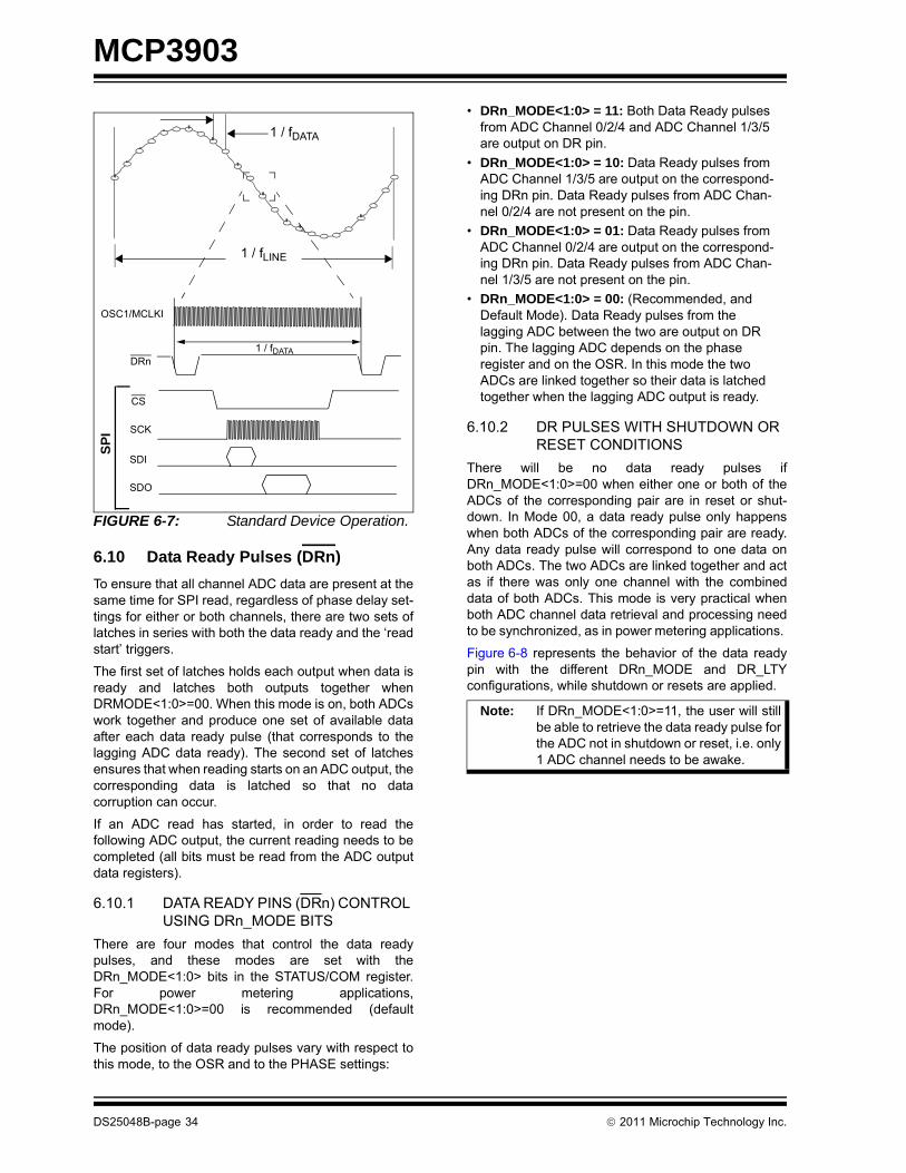
MCP3903
FIGURE 6-7: Standard Device Operation.
6.10 Data Ready Pulses (DRn)To ensure that all channel ADC data are present at thesame time for SPI read, regardless of phase delay set-tings for either or both channels, there are two sets oflatches in series with both the data ready and the ‘readstart’ triggers.
The first set of latches holds each output when data isready and latches both outputs together whenDRMODE<1:0>=00. When this mode is on, both ADCswork together and produce one set of available dataafter each data ready pulse (that corresponds to thelagging ADC data ready). The second set of latchesensures that when reading starts on an ADC output, thecorresponding data is latched so that no datacorruption can occur.
If an ADC read has started, in order to read thefollowing ADC output, the current reading needs to becompleted (all bits must be read from the ADC outputdata registers).
6.10.1 DATA READY PINS (DRn) CONTROL USING DRn_MODE BITS
There are four modes that control the data readypulses, and these modes are set with theDRn_MODE<1:0> bits in the STATUS/COM register.For power metering applications,DRn_MODE<1:0>=00 is recommended (defaultmode).
The position of data ready pulses vary with respect tothis mode, to the OSR and to the PHASE settings:
• DRn_MODE<1:0> = 11: Both Data Ready pulses from ADC Channel 0/2/4 and ADC Channel 1/3/5 are output on DR pin.
• DRn_MODE<1:0> = 10: Data Ready pulses from ADC Channel 1/3/5 are output on the correspond-ing DRn pin. Data Ready pulses from ADC Chan-nel 0/2/4 are not present on the pin.
• DRn_MODE<1:0> = 01: Data Ready pulses from ADC Channel 0/2/4 are output on the correspond-ing DRn pin. Data Ready pulses from ADC Chan-nel 1/3/5 are not present on the pin.
• DRn_MODE<1:0> = 00: (Recommended, and Default Mode). Data Ready pulses from the lagging ADC between the two are output on DR pin. The lagging ADC depends on the phase register and on the OSR. In this mode the two ADCs are linked together so their data is latched together when the lagging ADC output is ready.
6.10.2 DR PULSES WITH SHUTDOWN OR RESET CONDITIONS
There will be no data ready pulses ifDRn_MODE<1:0>=00 when either one or both of theADCs of the corresponding pair are in reset or shut-down. In Mode 00, a data ready pulse only happenswhen both ADCs of the corresponding pair are ready.Any data ready pulse will correspond to one data onboth ADCs. The two ADCs are linked together and actas if there was only one channel with the combineddata of both ADCs. This mode is very practical whenboth ADC channel data retrieval and processing needto be synchronized, as in power metering applications.
Figure 6-8 represents the behavior of the data readypin with the different DRn_MODE and DR_LTYconfigurations, while shutdown or resets are applied.
1 / fDATA
1 / fLINE
DRn1 / fDATA
OSC1/MCLKI
CS
SCK
SDI
SPI
SDO
Note: If DRn_MODE<1:0>=11, the user will stillbe able to retrieve the data ready pulse forthe ADC not in shutdown or reset, i.e. only1 ADC channel needs to be awake.
DS25048B-page 34 © 2011 Microchip Technology Inc.

MCP3903
FIGURE 6-8: Data Ready Behavior.
D0
D1
D2
D0
D1
D2
D3
D4
D5
D3
D4
D5
D0
D1
D2
D3
D4
D5
D6
D7
D8
D1
D3
D5
D6
D7
D8
D10
D12
D0
D2
D4
D9
D11
D13
D14
D6
D6
D12
D9
D13
D16
D17
D18
D19
D21
D24
D15
D20
D22
D25
D26
D7
D8
D9
D10
D11
D10
D11
D12
D10
D7
D8
D9
D23
D0
D1
D2
D3
D4
D5
D6
D7
D8
D9
D10
D11
D12
D13
D14
D15
D16
D17
D18
D19
D0
D1
D2
D3
D4
D5
D6
D7
D8
D9
D11
D10
D12
D13
D14
D15
D16
D0
D1
D2
D4
D5
D3
D7
D8
D9
D10
D11
D12
D13
D6
D15
D16
D14
D0
D1
D2
D6
D10
D11
D12
D13
D11
D13
D14
D15
D16
D12
D13
D14
D14
D28
D29
D31
D33
D27
D30
D32
D34
D15
D16
D17
D8
D7
D9
D4
D5
D3
RESET<1> or
SHU
TDO
WN
<1>
RESET<0> or
SHU
TDO
WN
<0>
RESET
D0
D1
D2
D3
D4
D5
D0
D1
D2
D3
D4
D5
D6
D7
D8
D1
D3
D5
D6
D7
D8
D11
D13
D0
D2
D4
D10
D12
D14
D15
D6
D9
D13
D17
D18
D21
D24
D16
D19
D22
D25
D26
D10
D11
D12
D10
D8
D9
D23
D11
D12
D13
D14
D28
D29
D31
D33
D27
D30
D32
D34
D14
D15
D16
D0
D1
D2
D3
D4
D5
D12
D11
D13
D15
D16
D17
D8
D9
D10
D7
PHASE < 0 PHASE = 0 PHASE > 0
D6
D7
DRCLK
periodD
RCLK period
Internal reset synchronisation (1 D
MCLK
period)
3*DRCLK
period3*D
RCLK period
D14
D9
D20
DRM
OD
E=00; DR
DRM
OD
E=01; DR
DRM
OD
E=10; DR
DRM
OD
E=11; DR
DRM
OD
E=00; DR
DRM
OD
E=01; DR
DRM
OD
E=10; DR
DRM
OD
E=11; DR
DRM
OD
E=00; DR
DRM
OD
E=01; DR
DRM
OD
E=10; DR
DRM
OD
E=11; DR
DRM
OD
E=00 : Select the lagging Data Ready
DRM
OD
E=01 : Select the Data Ready on channel 0
DRM
OD
E=10 : Select the Data Ready on channel 1
DRM
OD
E=11 : Select both Data ready
Data Ready pulse that appears only w
hen DR_LTY
=0
DRCLK
period1 D
MCLK
period
© 2011 Microchip Technology Inc. DS25048B-page 35

MCP3903
6.11 DATA READY PULSE WITHPHASE DELAY
To ensure that both channel ADC data from the samepair are present at the same time for SPI read, regard-less of phase delay settings for either or both channels,there are two sets of latches in series with both the dataready and the reading start triggers. The first latch is seton whichever channel is the lagging channel (relative tothe other channel, in a single channel pair). The secondlatch is set when an ADC output read command isissued, ensuring synchronized data ready pulses.
FIGURE 6-9: Internal Latches Synchronizing Data Ready Pulses with Phase Delay Present (Single Channel Pair Shown).
6.11.1 DATA READY LINKWhen DRLINK=0, the three pairs of ADCs areindependent from each other. The data readys and thelatches for the output data only depend on both ADCsin the pair. When another ADC (not in the pair) is put inSHUTDOWN or RESET, it has no effect.
When DRLINK=1, all ADCs are linked together. TheDRn_MODE<1:0> are all set internally to 00. AllDRn_MODE<1:0> bits are not taken into account.
All six channel ADC data are latched synchronouslywith the most lagging ADC channel of the six.
All three DRA, DRB and DRC data ready pins aregiving the same output that is synchronized with themost lagging ADC of the six channels. Only one pin canbe connected to the MCU in this mode, which savestwo connection ports on the MCU.
In this mode, if any channel is in SHUTDOWN orRESET mode, no data ready is present on any of theDRA/DRB/DRC pins. The part acts as if there was onlyone ADC channel with 6x24 bits.
Depending on the read modes, the ADC data can beretrieved by pair (Read by GROUP) or all together(Read by TYPE). Any time a new read command is per-formed, the ADC outputs are re-latched. In order toavoid loss of data or bad synchronization, the readmode by TYPES is recommended (READ<1:0>=10) sothat all data can be latched once at the beginning of theread. In the read mode by GROUP (READ<1:0>=01)mode, the data will be relatched every time the partaccesses to each group or pair of ADCs.
CHn ADC LATCH SPI SerialInterface
CHn ADC LATCH
Synchronizeddata ready pulses
DS25048B-page 36 © 2011 Microchip Technology Inc.

MCP3903
7.0 INTERNAL REGISTERSThe addresses associated with the internal registersare listed below. All registers are 24 bits long and canbe addressed separately. A detailed description of theregisters follows. .
The following table shows how the internal addresscounter will loop on specific register groups and types.
7.1 Channel Output Registers
The ADC Channel data output registers always containthe most recent A/D conversion data for each channel.These registers are read-only. They can be accessedindependently or linked together (with READ<1:0>bits). These registers are latched when an ADC readcommunication occurs. When a data ready eventoccurs during a read communication, the most currentADC data is also latched to avoid data corruptionissues. The three bytes of each channel are updatedsynchronously at a DRCLK rate. The three bytes canbe accessed separately if needed, but are refreshedsynchronously. The coding is 23-bit + sign two’scomplement (see Section 5.5).
TABLE 7-1: INTERNAL REGISTER SUMMARYAddress Name Bits R/W Description
0x00 CHANNEL 0 24 R Channel 0 ADC Data <23:0>, MSB first, left justified0x01 CHANNEL 1 24 R Channel 1 ADC Data <23:0>, MSB first, left justified0x02 CHANNEL 2 24 R Channel 2 ADC Data <23:0>, MSB first, left justified0x03 CHANNEL 3 24 R Channel 3 ADC Data <23:0>, MSB first, left justified0x04 CHANNEL 4 24 R Channel 4 ADC Data <23:0>, MSB first, left justified0x05 CHANNEL 5 24 R Channel 5 ADC Data <23:0>, MSB first, left justified0x06 MOD 24 R/W Delta Sigma Modulators Output Value 0x07 PHASE 24 R/W Phase Delay Configuration Register0x08 GAIN 24 R/W Gain Configuration Register0x09 STATUS/COM 24 R/W Status/Communication Register0x0A CONFIG 24 R/W Configuration Register
TABLE 7-2: CONTINUOUS READ OPTIONS, LOOPING ON INTERNAL ADDRESSES
Function AddressREAD<1:0>
= “01” = “10” =“11”
CHANNEL 0 0x00GROUP
TYP
E
LOO
P E
NTI
RE
RE
GIS
TER
MA
PCHANNEL 1 0x01CHANNEL 2 0x02
GROUPCHANNEL 3 0x03CHANNEL 4 0x04
GROUPCHANNEL 5 0x05
MOD 0x06
GR
OU
P
TYP
E
PHASE 0x07GAIN 0x08
STATUS/COM
0x09
GR
OU
P
CONFIG 0x0A
TABLE 7-3: ADC OUTPUT REGISTERSName Bits Address Cof
CHANNEL 0 24 0x00 R
CHANNEL 1 24 0x01 R
CHANNEL 2 24 0x02 R
CHANNEL 3 24 0x03 R
CHANNEL 4 24 0x04 R
CHANNEL 5 24 0x05 R
© 2011 Microchip Technology Inc. DS25048B-page 37

MCP3903
REGISTER 7-1: CHANNEL REGISTERR-0 R-0 R-0 R-0 R-0 R-0 R-0 R-0D23 (MSB) D22 D21 D20 D19 D18 D17 D16
bit 23 bit 16
R-0 R-0 R-0 R-0 R-0 R-0 R-0 R-0D15 D14 D13 D12 D11 D10 D9 D8
bit 15 bit 8
R-0 R-0 R-0 R-0 R-0 R-0 R-0 R-0D7 D6 D5 D4 D3 D2 D1 D0
bit 7 bit 0
Legend:R = Readable bit W = Writable bit U = Unimplemented bit, read as ‘0’-n = Value at POR ‘1’ = Bit is set ‘0’ = Bit is cleared x = Bit is unknown
bit 23:0 24-bit ADC output data of the corresponding channel
DS25048B-page 38 © 2011 Microchip Technology Inc.

MCP3903
7.2 Mod RegisterThe MOD register contains the most recent modulatordata output. The default value corresponds to anequivalent input of 0V on each ADC. Each bit in thisregister corresponds to one comparator output on oneof the channels.
This register should be used as a read-only register.
(Note 1). This register is updated at the refresh rate ofDMCLK (typically 1 MHz with MCLK = 4 MHz). Thedefault state for this register is001100110011001100110011.
TABLE 7-4: MODULATOR OUTPUT REGISTER
Name Bits Address CofMOD 24 0x06 R/W
REGISTER 7-2: MOD REGISTER
R/W-0 R/W-0 R/W-1 R/W-1 R/W-0 R/W-0 R/W-1 R/W-1COMP3_CH5 COMP2_CH5 COMP1_CH5 COMP0_CH5 COMP3_CH4 COMP2_CH4 COMP1_CH4 COMP0_CH4
bit 23 bit 16
R/W-0 R/W-0 R/W-1 R/W-1 R/W-0 R/W-0 R/W-1 R/W-1COMP3_CH3 COMP2_CH3 COMP1_CH3 COMP0_CH3 COMP3_CH2 COMP2_CH2 COMP1_CH2 COMP0_CH2
bit 15 bit 8
R/W-0 R/W-0 R/W-1 R/W-1 R/W-0 R/W-0 R/W-1 R/W-1COMP3_CH1 COMP2_CH1 COMP1_CH1 COMP0_CH1 COMP3_CH1 COMP2_CH0 COMP1_CH0 COMP0_CH0
bit 7 bit 0
Legend:R = Readable bit W = Writable bit U = Unimplemented bit, read as ‘0’-n = Value at POR ‘1’ = Bit is set ‘0’ = Bit is cleared x = Bit is unknown
bit 23:20 COMPn_CH5: Comparator Outputs from ADC Channel 5bit 19:16 COMPn_CH4: Comparator Outputs from ADC Channel 4bit 15:12 COMPn_CH3: Comparator Outputs from ADC Channel 3bit 11:8 COMPn_CH2: Comparator Outputs from ADC Channel 2bit 7:4 COMPn_CH1: Comparator Outputs from ADC Channel 1bit 3:0 COMPn_CH0: Comparator Outputs from ADC Channel 0
© 2011 Microchip Technology Inc. DS25048B-page 39

MCP3903
7.3 Phase RegisterThe phase register is composed of three bytes:PHASEC<7:0>, PHASEB<7:0>, PHASEA<7:0>. Eachbyte is a 7 bit + sign MSB first, two's complement codethat represents the amount of delay between each pairof ADCs. The PHASEC byte represents the delaybetween Channel 4 and Channel 5 (pair C). ThePHASEB byte represents the delay between Channel 2and Channel 3 (pair B). The PHASEA byte representsthe delay between Channel 0 and Channel 1 (pair A).
The reference channel is the odd channel (Channel 1/3/5). When PHASEn<7:0> is positive, Channel 0/2/4 islagging versus channel 1/3/5 otherwise it is leading.
The delay is calculated by the following formula:
Delay = PHASE Register Code / DMCLK.
TABLE 7-5: PHASE REGISTERName Bits Address Cof
PHASE 24 0x07 R/W
REGISTER 7-3: PHASE REGISTER
R/W-0 R/W-0 R/W-0 R/W-0 R/W-0 R/W-0 R/W-0 R/W-0PHASEC7 PHASEC6 PHASEC5 PHASEC4 PHASEC3 PHASEC2 PHASEC1 PHASEC0
bit 23 bit 16
R/W-0 R/W-0 R/W-0 R/W-0 R/W-0 R/W-0 R/W-0 R/W-0PHASEB7 PHASEB6 PHASEB5 PHASEB4 PHASEB3 PHASEB2 PHASEB1 PHASEB0
bit 15 bit 8
R/W-0 R/W-0 R/W-0 R/W-0 R/W-0 R/W-0 R/W-0 R/W-0PHASEA7 PHASEA6 PHASEA5 PHASEA4 PHASEA3 PHASEA2 PHASEA1 PHASEA0
bit 7 bit 0
Legend:R = Readable bit W = Writable bit U = Unimplemented bit, read as ‘0’-n = Value at POR ‘1’ = Bit is set ‘0’ = Bit is cleared x = Bit is unknown
bit 23:16 PHASECn: CH4 relative to CH5 phase delay bit 15:8 PHASEBn: CH2 relative to CH3 phase delaybit 7:0 PHASEAn: CH0 relative to CH1 phase delay
DS25048B-page 40 © 2011 Microchip Technology Inc.

MCP3903
7.4 Gain Configuration RegisterThis register contains the gain register
TABLE 7-6: GAIN REGISTERName Bits Address CofGAIN 24 0x08 R/W
REGISTER 7-4: GAIN REGISTER
R/W-0 R/W-0 R/W-0 R/W-0 R/W-0 R/W-0 R/W-0 R/W-0PGA2_CH5 PGA1_CH5 PGA0_CH5 BOOST_ CH5 BOOST_ CH4 PGA2_CH4 PGA1_CH4 PGA0_CH4
bit 23 bit 16
R/W-0 R/W-0 R/W-0 R/W-0 R/W-0 R/W-0 R/W-0 R/W-0PGA2_CH3 PGA1_CH3 PGA0_CH3 BOOST_ CH3 BOOST_ CH2 PGA2_CH2 PGA1_CH2 PGA0_CH2
bit 15 bit 8
R/W-0 R/W-0 R/W-0 R/W-0 R/W-0 R/W-0 R/W-0 R/W-0PGA2_CH1 PGA1_CH1 PGA0_CH1 BOOST_ CH1 BOOST_ CH0 PGA2_CH0 PGA1_CH0 PGA0_CH0
bit 7 bit 0
Legend:R = Readable bit W = Writable bit U = Unimplemented bit, read as ‘0’-n = Value at POR ‘1’ = Bit is set ‘0’ = Bit is cleared x = Bit is unknown
bit PGA_CHn: PGA Setting for Channel n111 = Reserved (Gain = 1)110 = Reserved (Gain = 1)101 = Gain is 32100 = Gain is 16011 = Gain is 8010 = Gain is 4001 = Gain is 2000 = Gain is 1
bit BOOST_CHn Current Scaling for high speed operation for channel n1 = Channel has current x 2 0 = Channel has normal current
© 2011 Microchip Technology Inc. DS25048B-page 41

MCP3903
7.5 STATUS/COM Register - Statusand Communication Register
7.5.1 DATA READY LATENCY - DR_LTYThis bit determines if the data ready pulses correspondto settled data or unsettled data from each SINC3 filter.Unsettled data will provide data ready pulses everyDRCLK period. Settled data will wait for 3 DRCLKperiods before giving data ready pulses and will thengive data ready pulses every DRCLK period.
7.5.2 DATA READY HIGH Z MODE - DR_HIZ
Using this bit, the user can connect multiple chips withthe same data ready pin with a pull up resistor(DR_HIZ=0) or a single chip with no external compo-nent (DR_HIZ=1)
7.5.3 DATA READY MODE - DRN_MODEThese bits control which ADC data ready is present onthe data ready pin. When the bits are set to 00, theoutput of the two ADCs are latched synchronously atthe moment of the data ready event. This prevents badsynchronization between the two ADCs. The output isalso latched at the beginning of a reading, in order notto be updated during a read, and not to give erroneousdata.
If one of the channels is in reset or shutdown, only oneof the data ready pulses is present and the situation issimilar to DRn_MODE<1:0> = 01 or 10. In the 01,10and 11 modes, the data is latched at the beginning of areading, in order to prevent the case of erroneous datawhen a data ready pulse happens when reading.
7.5.4 DATA READY STATUS FLAG - DRSTATUS_CHN
These bits indicate the data ready status of each chan-nel. These flags are set to logic high after being theSTATUS/COM register has been read. These bits arecleared when a data ready event has happened on itsrespective ADC. Writing these bits has no effect.
TABLE 7-7: STATUS/COM RegisterName Bits Address Cof
STATUS/COM 24 0x09 R/W
Note: These bits are useful if multiple devicesshare the same DRn output pin(DR_HIZ=0) in order to understand whichdevice the data ready event occured from.In case the DRn_MODE=00 (LinkedADCs), these data ready status bits will beupdated synchronously upon the sameevent (lagging ADC is ready). These bitsare also useful in systems where the DRnpins are not used to save MCU I/O.
REGISTER 7-5: STATUS/COM REGISTER
R/W-1 R/W-0 R/W-0 R/W-0 R/W-0 R/W-0 R/W-0 R/W-0
READ1 READ0 WMODE WIDTH_CH5 WIDTH_CH4 WIDTH_CH3 WIDTH_CH2 WIDTH_CH1
bit 23 bit 16
R/W-0 R/W-1 R/W-0 R/W-0 R/W-0 R/W-0 R/W-0 R/W-0
WIDTH_CH0 DR_LTY DR_HIZ DR_LINK DRC_MODE1 DRC_MODE0 DRB_MODE1 DRB_MODE0
bit 15 bit 8
R/W-0 R/W-0 R-1 R-1 R-1 R-1 R-1 R-1
DRA_MODE1 DRA_MODE0 DRSTATUS_CH5 DRSTATUS_CH4 DRSTATUS_CH3 DRSTATUS_CH2 DRSTATUS_CH1 DRSTATUS_CH0
bit 7 bit 0
bit 23:22 READ[1:0]: Address Loop Setting11 = Address counter incremented, cycle through entire register map10 = Address counter loops on register TYPES (DEFAULT)01 = Address counter loops on register GROUPS00 = Address not incremented, continually read single register
bit 21 WMODE: Write Mode Bit (internal use only)1 = Static addressing Write Mode0 = Incremental addressing Write Mode (DEFAULT)
DS25048B-page 42 © 2011 Microchip Technology Inc.

MCP3903
bit 20:15 WIDTH_CHn ADC Channels output data word width control1 = 24-bit mode for the corresponding channel0 = 16-bit mode for the corresponding channel (default)
bit 14 DR_LTY: Data Ready Latency Control for DRA, DRB, and DRC pins1 = True “No Latency” Conversion, data ready pulses after 3 DRCLK periods (DEFAULT)0 = Unsettled Data is available after every DRCLK period
bit 13 DR_HIZ: Data Ready Pin Inactive State Control for DRA, DRB, and DRC pins1 = The Default state is a logic high when data is NOT ready0 = The Default state is high impedance when data is NOT ready (DEFAULT)
bit 12 DR_LINK Data Ready Link Control1 = Data Ready Link turned ON, all channels linked and data ready pulses from the most lagging ADC
are present on each DRn pin0 = Data Ready Link tunred OFF (DEFAULT)
bit 11:10 DRC_MODE[1:0]11 = Both Data Ready pulses from CH4 and CH5 are output on DRC pin. 10 = Data Ready pulses from CH5 are output on DRC pin. Data Ready pulses R from CH4 are not pres-
ent on the pin.01 = Data Ready pulses from CH4 are output on DRC pin. Data Ready pulses from CH5 are not present
on the pin.00 = Data Ready pulses from the lagging ADC channel between the two are output on DRC pin. The
lagging ADC channel depends on the phase register and on the OSR. (DEFAULT)bit 9:8 DRB_MODE[1:0]
11 = Both Data Ready pulses from CH2 and CH3 are output on DRB pin. 10 = Data Ready pulses from CH3 are output on DRB pin. Data Ready pulses from CH2 are not present
on the pin.01 = Data Ready pulses from CH2 are output on DRB pin. Data Ready pulses from CH3 are not present
on the pin.00 = Data Ready pulses from the lagging ADC channel between the two are output on DRB pin. The
lagging ADC channel depends on the phase register and on the OSR. (DEFAULT)bit 7:6 DRA_MODE[1:0]
11 = Both Data Ready pulses from CH0 and CH1 are output on DRA pin. 10 = Data Ready pulses from CH1 are output on DRA pin. Data Ready pulses from CH0 are not present
on the pin.01 = Data Ready pulses from CH0 are output on DRA pin. Data Ready pulses from CH1 are not present
on the pin.00 = Data Ready pulses from the lagging ADC channel between the two are output on DRA pin. The
lagging ADC channel depends on the phase register and on the OSR. (DEFAULT)bit 5:0 DRSTATUS_CHn: Data Ready Status
1 = Data Not Ready (default)0 = Data Ready
REGISTER 7-5: STATUS/COM REGISTER (CONTINUED)
© 2011 Microchip Technology Inc. DS25048B-page 43

MCP3903
7.6 Config Register - ConfigurationRegister
TABLE 7-8: CONFIG RegisterName Bits Address Cof
CONFIG 24 0x0A R/W
REGISTER 7-6: CONFIG REGISTER
R/W-0 R/W-0 R/W-0 R/W-0 R/W-0 R/W-0 R/W-0 R/W-0
RESET_CH5 RESET_CH4 RESET_CH3 RESET_CH2 RESET_CH1 RESET_CH0 SHUTDOWN_CH5 SHUTDOWN_CH4
bit 23 bit 16
R/W-0 R/W-0 R/W-0 R/W-0 R/W-1 R/W-1 R/W-1 R/W-1
SHUTDOWN_CH3
SHUTDOWN_CH2
SHUTDOWN_CH1 SHUTDOWN_CH0 DITHER_CH5 DITHER_CH4 DITHER_CH3 DITHER_CH2
bit 15 bit 8
R/W-1 R/W-1 R/W-0 R/W-1 R/W-0 R/W-0 R/W-0 R/W-0
DITHER_CH1 DITHER_CH0 OSR1 OSR0 PRESCALE1 PRESCALE0 EXTVREF EXTCLK
bit 7 bit 0
bit 23:18 RESET_CHn: Reset mode setting for ADCs1 = Reset mode for the corresponding ADC channel ON0 = Reset mode for the corresponding ADC chnnel OFF (default)
bit 17:12 SHUTDOWN_CHn: Shutdown mode setting for ADCs1 = Shutdown mode for the corresponding ADC channel ON0 = Shutdown mode for the corresponding ADC channel OFF(default)
bit 11:6 DITHER_CHn: Control for dithering circuit for idle tones cancellation1 = Dithering circuit for the corresponding ADC channel ON (default)0 = Dithering circuit for the corresponding ADC channel OFF
bit 5:4 OSR[1:0] Oversampling Ratio for Delta Sigma A/D Conversion (ALL CHANNELS, fd / fS)11 = 25610 = 12801 = 64 (default) 00 = 32
bit 3:2 PRESCALE[1:0] Internal Master Clock (AMCLK) Prescaler Value 11 = AMCLK = MCLK/ 810 = AMCLK = MCLK/ 401 = AMCLK = MCLK/ 200 = AMCLK = MCLK (DEFAULT)
bit 1 EXTVREF Internal Voltage Reference Shutdown Control1 = Internal Voltage Reference Disabled0 = Internal Voltage Reference Enabled (default)
bit 0 EXTCLK Clock Mode1 = CLOCK Mode (Internal Oscillator Disabled - Lower Power)0 = XT Mode - A crystal must be placed between OSC1/OSC2 (default)
DS25048B-page 44 © 2011 Microchip Technology Inc.

MCP3903
8.0 PACKAGING INFORMATION
8.1 Package Marking Information
Legend: XX...X Customer-specific informationY Year code (last digit of calendar year)YY Year code (last 2 digits of calendar year)WW Week code (week of January 1 is week ‘01’)NNN Alphanumeric traceability code Pb-free JEDEC designator for Matte Tin (Sn)* This package is Pb-free. The Pb-free JEDEC designator ( )
can be found on the outer packaging for this package.
Note: In the event the full Microchip part number cannot be marked on one line, it willbe carried over to the next line, thus limiting the number of availablecharacters for customer-specific information.
3e
3e
28-Lead SSOP (5.30 mm) Example
MCP3903
3eE/SS
1124256
28-Lead SSOP (5.30 mm) Example
MCP3903
3eI/SS
1124256
© 2011 Microchip Technology Inc. DS25048B-page 45

MCP3903
!"#
$ % !"# $% &" ' ()"&'"!&) & #*&& & # ' !!#+#&"# '#%!&"!!#%!&"!!!& $ #'' !# , ' !#& +-.
/01 /!' ! & $& " !**&"&& !+21 % ' !("!"*&"&& (%%'&"! !
$ % 2& '!&" &3 #*!( ! ! & 3 %&& #&&&144***''43
5&! 66++' !6'&! 7 78 9
7"') %! 7 :& ./08 ; & < < # #3 3 !! . . :.&#%% . < <8 =#& + : :# #3 =#& + . ., .8 6 & .2&6 & 6 .. . .2&& 6 .+26 #3 !! < .2& > > :>6 #=#& ) < ,:
LL1
cA2
A1
A
EE1
D
N
1 2
NOTE 1b
e
φ
* 0,/
DS25048B-page 46 © 2011 Microchip Technology Inc.

MCP3903
Note: For the most current package drawings, please see the Microchip Packaging Specification located at http://www.microchip.com/packaging
© 2011 Microchip Technology Inc. DS25048B-page 47

MCP3903
DS25048B-page 48 © 2011 Microchip Technology Inc.

MCP3903
APPENDIX A: REVISION HISTORY
Revision B (July 2011)• Added Section 2.0, Typical Performance
Curves, with characterization graphs.
Revision A (June 2011)• Original data sheet for the MCP3903 device.
© 2011 Microchip Technology Inc. DS25048B-page 51

MCP3903
NOTES:DS25048B-page 52 © 2011 Microchip Technology Inc.

MCP3903
PRODUCT IDENTIFICATION SYSTEMTo order or obtain information, e.g., on pricing or delivery, refer to the factory or the listed sales office.
Device: MCP3903: Six Channel ΔΣ A/D Converter
* Default option. Contact Microchip factory for other address options
Tape and Reel: T = Tape and Reel
Temperature Range: I = -40°C to +85°C
E = -40°C to +125°C
Package: SS = Small Shrink Output Package (SSOP-28)
Examples:a) MCP3903T-E/SS: Tape and Reel,
Six Channel ΔΣ A/DConverter,SSOP-28 package
b) MCP3903T-I/SS: Tape and Reel,Six Channel ΔΣ A/DConverter,SSOP-28 package
PART NO. X
TemperatureRange
Device
/XX
Package
X
Tape andReel
© 2011 Microchip Technology Inc. DS25048B-page 53

MCP3903
NOTES:DS25048B-page 54 © 2011 Microchip Technology Inc.

Note the following details of the code protection feature on Microchip devices:• Microchip products meet the specification contained in their particular Microchip Data Sheet.
• Microchip believes that its family of products is one of the most secure families of its kind on the market today, when used in the intended manner and under normal conditions.
• There are dishonest and possibly illegal methods used to breach the code protection feature. All of these methods, to our knowledge, require using the Microchip products in a manner outside the operating specifications contained in Microchip’s Data Sheets. Most likely, the person doing so is engaged in theft of intellectual property.
• Microchip is willing to work with the customer who is concerned about the integrity of their code.
• Neither Microchip nor any other semiconductor manufacturer can guarantee the security of their code. Code protection does not mean that we are guaranteeing the product as “unbreakable.”
Code protection is constantly evolving. We at Microchip are committed to continuously improving the code protection features of ourproducts. Attempts to break Microchip’s code protection feature may be a violation of the Digital Millennium Copyright Act. If such actsallow unauthorized access to your software or other copyrighted work, you may have a right to sue for relief under that Act.
Information contained in this publication regarding deviceapplications and the like is provided only for your convenienceand may be superseded by updates. It is your responsibility toensure that your application meets with your specifications.MICROCHIP MAKES NO REPRESENTATIONS ORWARRANTIES OF ANY KIND WHETHER EXPRESS ORIMPLIED, WRITTEN OR ORAL, STATUTORY OROTHERWISE, RELATED TO THE INFORMATION,INCLUDING BUT NOT LIMITED TO ITS CONDITION,QUALITY, PERFORMANCE, MERCHANTABILITY ORFITNESS FOR PURPOSE. Microchip disclaims all liabilityarising from this information and its use. Use of Microchipdevices in life support and/or safety applications is entirely atthe buyer’s risk, and the buyer agrees to defend, indemnify andhold harmless Microchip from any and all damages, claims,suits, or expenses resulting from such use. No licenses areconveyed, implicitly or otherwise, under any Microchipintellectual property rights.
© 2011 Microchip Technology Inc.
Trademarks
The Microchip name and logo, the Microchip logo, dsPIC, KEELOQ, KEELOQ logo, MPLAB, PIC, PICmicro, PICSTART, PIC32 logo, rfPIC and UNI/O are registered trademarks of Microchip Technology Incorporated in the U.S.A. and other countries.
FilterLab, Hampshire, HI-TECH C, Linear Active Thermistor, MXDEV, MXLAB, SEEVAL and The Embedded Control Solutions Company are registered trademarks of Microchip Technology Incorporated in the U.S.A.
Analog-for-the-Digital Age, Application Maestro, chipKIT, chipKIT logo, CodeGuard, dsPICDEM, dsPICDEM.net, dsPICworks, dsSPEAK, ECAN, ECONOMONITOR, FanSense, HI-TIDE, In-Circuit Serial Programming, ICSP, Mindi, MiWi, MPASM, MPLAB Certified logo, MPLIB, MPLINK, mTouch, Omniscient Code Generation, PICC, PICC-18, PICDEM, PICDEM.net, PICkit, PICtail, REAL ICE, rfLAB, Select Mode, Total Endurance, TSHARC, UniWinDriver, WiperLock and ZENA are trademarks of Microchip Technology Incorporated in the U.S.A. and other countries.
SQTP is a service mark of Microchip Technology Incorporated in the U.S.A.
All other trademarks mentioned herein are property of their respective companies.
© 2011, Microchip Technology Incorporated, Printed in the U.S.A., All Rights Reserved.
Printed on recycled paper.
ISBN: 978-1-61341-402-6
DS25048B-page 55
Microchip received ISO/TS-16949:2009 certification for its worldwide headquarters, design and wafer fabrication facilities in Chandler and Tempe, Arizona; Gresham, Oregon and design centers in California and India. The Company’s quality system processes and procedures are for its PIC® MCUs and dsPIC® DSCs, KEELOQ® code hopping devices, Serial EEPROMs, microperipherals, nonvolatile memory and analog products. In addition, Microchip’s quality system for the design and manufacture of development systems is ISO 9001:2000 certified.

DS25048B-page 56 © 2011 Microchip Technology Inc.
AMERICASCorporate Office2355 West Chandler Blvd.Chandler, AZ 85224-6199Tel: 480-792-7200 Fax: 480-792-7277Technical Support: http://www.microchip.com/supportWeb Address: www.microchip.comAtlantaDuluth, GA Tel: 678-957-9614 Fax: 678-957-1455BostonWestborough, MA Tel: 774-760-0087 Fax: 774-760-0088ChicagoItasca, IL Tel: 630-285-0071 Fax: 630-285-0075ClevelandIndependence, OH Tel: 216-447-0464 Fax: 216-447-0643DallasAddison, TX Tel: 972-818-7423 Fax: 972-818-2924DetroitFarmington Hills, MI Tel: 248-538-2250Fax: 248-538-2260IndianapolisNoblesville, IN Tel: 317-773-8323Fax: 317-773-5453Los AngelesMission Viejo, CA Tel: 949-462-9523 Fax: 949-462-9608Santa ClaraSanta Clara, CA Tel: 408-961-6444Fax: 408-961-6445TorontoMississauga, Ontario, CanadaTel: 905-673-0699 Fax: 905-673-6509
ASIA/PACIFICAsia Pacific OfficeSuites 3707-14, 37th FloorTower 6, The GatewayHarbour City, KowloonHong KongTel: 852-2401-1200Fax: 852-2401-3431Australia - SydneyTel: 61-2-9868-6733Fax: 61-2-9868-6755China - BeijingTel: 86-10-8569-7000 Fax: 86-10-8528-2104China - ChengduTel: 86-28-8665-5511Fax: 86-28-8665-7889China - ChongqingTel: 86-23-8980-9588Fax: 86-23-8980-9500China - HangzhouTel: 86-571-2819-3180 Fax: 86-571-2819-3189China - Hong Kong SARTel: 852-2401-1200 Fax: 852-2401-3431China - NanjingTel: 86-25-8473-2460Fax: 86-25-8473-2470China - QingdaoTel: 86-532-8502-7355Fax: 86-532-8502-7205China - ShanghaiTel: 86-21-5407-5533 Fax: 86-21-5407-5066China - ShenyangTel: 86-24-2334-2829Fax: 86-24-2334-2393China - ShenzhenTel: 86-755-8203-2660 Fax: 86-755-8203-1760China - WuhanTel: 86-27-5980-5300Fax: 86-27-5980-5118China - XianTel: 86-29-8833-7252Fax: 86-29-8833-7256China - XiamenTel: 86-592-2388138 Fax: 86-592-2388130China - ZhuhaiTel: 86-756-3210040 Fax: 86-756-3210049
ASIA/PACIFICIndia - BangaloreTel: 91-80-3090-4444 Fax: 91-80-3090-4123India - New DelhiTel: 91-11-4160-8631Fax: 91-11-4160-8632India - PuneTel: 91-20-2566-1512Fax: 91-20-2566-1513Japan - YokohamaTel: 81-45-471- 6166 Fax: 81-45-471-6122Korea - DaeguTel: 82-53-744-4301Fax: 82-53-744-4302Korea - SeoulTel: 82-2-554-7200Fax: 82-2-558-5932 or 82-2-558-5934Malaysia - Kuala LumpurTel: 60-3-6201-9857Fax: 60-3-6201-9859Malaysia - PenangTel: 60-4-227-8870Fax: 60-4-227-4068Philippines - ManilaTel: 63-2-634-9065Fax: 63-2-634-9069SingaporeTel: 65-6334-8870Fax: 65-6334-8850Taiwan - Hsin ChuTel: 886-3-6578-300Fax: 886-3-6578-370Taiwan - KaohsiungTel: 886-7-213-7830Fax: 886-7-330-9305Taiwan - TaipeiTel: 886-2-2500-6610 Fax: 886-2-2508-0102Thailand - BangkokTel: 66-2-694-1351Fax: 66-2-694-1350
EUROPEAustria - WelsTel: 43-7242-2244-39Fax: 43-7242-2244-393Denmark - CopenhagenTel: 45-4450-2828 Fax: 45-4485-2829France - ParisTel: 33-1-69-53-63-20 Fax: 33-1-69-30-90-79Germany - MunichTel: 49-89-627-144-0 Fax: 49-89-627-144-44Italy - Milan Tel: 39-0331-742611 Fax: 39-0331-466781Netherlands - DrunenTel: 31-416-690399 Fax: 31-416-690340Spain - MadridTel: 34-91-708-08-90Fax: 34-91-708-08-91UK - WokinghamTel: 44-118-921-5869Fax: 44-118-921-5820
Worldwide Sales and Service
05/02/11