size reduction of dc-dc converter using flying capacitor...
TRANSCRIPT

IEEJ Journal of Industry ApplicationsVol.3 No.6 pp.446–454 DOI: 10.1541/ieejjia.3.446
Paper
Size Reduction of DC-DC Converter using Flying Capacitor Topologywith Small Capacitance
Asmarashid Bin Ponniran∗ Student Member, Koichi Matsuura∗ Non-member
Koji Orikawa∗ Member, Jun-ichi Itoh∗a)Member
(Manuscript received Dec. 24, 2013, revised May 14, 2014)
The purpose of the present paper is to analyze the input inductor design and to establish the relationship betweenthe capacitance of the flying capacitor and the output voltage ripple in order to reduce the size and weight of the flyingcapacitor DC-DC boost converter (FCBC). The inductance of the input inductor is designed by considering the max-imum input current ripple, and the experimental results are used to confirm that the input current ripple is within thedesigned value. Furthermore, according to the design specifications, the required inductance of an input inductor isapproximately 25% of that of a conventional two-level DC-DC boost converter, and the required inductor core volumeis approximately 35% of that of a conventional two-level DC-DC boost converter. Moreover, the capacitance of the fly-ing capacitor and the output voltage ripple are confirmed to be independent of each other. Theoretically, this is becausethe time constant of the output capacitance and the output resistance of the FCBC is larger than the switching periodof the switching frequency. This finding is confirmed by the simulation and experimental results of the present study.On the basis of this finding, the capacitance of the flying capacitor can be estimated and designed without consideringthe output voltage ripple. Moreover, the achieved maximum efficiency of the designed FCBC is 98.5% of the outputpower at 1 kW.
Keywords: inductor size, flying capacitor, output voltage ripple, flying capacitor boost chopper
1. Introduction
In general, as a power converter, the DC-DC boost con-verter is important in high-power-capacity applications, suchas solar electric systems and electric vehicle systems. Thesetypes of applications typically demand high conversion effi-ciency with low weight, volume, and cost of the converter.Nevertheless, if a conventional DC-DC boost converter isconsidered, the bulkiness of the input inductor must be takeninto consideration because a typical conventional DC-DCboost converter requires large inductors for energy storage,especially for continuous-current-mode operation of the in-put current. Although conventional DC-DC boost convertersare evolving due to these drawbacks, the flying capacitor DC-DC boost converter (FCBC) has become a possible option.The FCBC with an input inductor has several advantages overa conventional DC-DC boost converter. The FCBC requiresonly a small input inductor and the suppression of an inputinrush current due to the existing of an input inductor com-pared to a conventional FCBC without an input inductor (1)–(4).
In addition, a number of researchers have reported thatinterleaved circuit topologies can be considered for conven-tional DC-DC boost converters. As a result, the input currentcan be reduced based on the number of interleaved circuits.
a) Correspondence to: Jun-ichi Itoh. E-mail: [email protected]∗ Nagaoka University of Technology
1603-1, Kamitomioka-machi, Nagaoka, Niigata 940-2188,Japan
Consequently, the inductance and core volume of the in-put inductors can be reduced (5)–(9). Moreover, by consider-ing multilevel structure topologies on the FCBC, the induc-tance and core volume of the input inductors can also bereduced (1)–(4). However, the interleaved circuit topology andmultilevel circuit structure introduce circuit complexity. Fur-thermore, such topologies require additional inductors, ca-pacitors, and switching devices, as well as other componentsand devices. Nevertheless, if a very-high-efficiency DC-DCboost converter is critical, regardless of size and weight, suchtopologies might be an option (1) (4)–(9).
Therefore, for single-phase operation and simplicity of theconverter circuit, the FCBC offers a good option due to theneed for fewer passive components and switching devices. Inaddition, by considering appropriate designs of the passivecomponents and devices, the sizes and volumes of the com-ponents and devices can be minimized.
As in the case of a conventional DC-DC boost converter,the output voltage in the FCBC can be controlled by control-ling the duty ratio of the switching signals. One importantfeature of the FCBC is that the boost-up energy is transferredfrom the flying capacitor to the output side, which meansthat the input inductor can be designed with small inductanceand a reduced inductor core volume (1) (4) (10). Consequently, theoverall size and weight of the input inductor can be greatlyreduced as compared to a conventional DC-DC boost con-verter (3) (10). Moreover, the power loss in terms of copper lossis also reduced as a result of fewer winding of the input induc-tor. Generally, passive components and devices in the FCBC,
c© 2014 The Institute of Electrical Engineers of Japan. 446

Flying Capacitor Topology with Small Capacitance(Asmarashid Bin Ponniran et al.)
i.e., the input inductor, the flying capacitor, and the outputcapacitor, must be designed correctly because these compo-nents will have a significant impact on converter operationand efficiency. However, this has not been clarified in previ-ous studies (1)–(3) (10)–(12).
Moreover, establishing the relationship between the ca-pacitance of the flying capacitor and the output voltage rip-ple is also important. Unfortunately, this has not been dis-cussed in other studies (1) (3) (4) (13) (14). Converter circuit compo-nents/devices and electrical parameters are significantly re-lated. Therefore, procedures for device estimation and de-sign must be established. Generally, the output voltage rippleshould be considered as a factor that influences the estimationof the capacitance of the flying capacitor in the FCBC (15) (16).Hence, the parametric relationship between the capacitanceof the flying capacitor and the output capacitance from theoutput voltage ripple must to be analyzed.
In the present paper, an FCBC is proposed considering asmall capacitance of the flying capacitor in order to reducethe size of the power converter. Principally, a small capac-itance of the flying capacitor causes a large voltage rippleacross the flying capacitor. In contrast, the voltage stressincreases when a small capacitance of the flying capacitoris used. However, low-power-loss and high-voltage powerdevices, such as SiC-MOSFETs, have recently been devel-oped. Thus, downsizing is a higher priority than the use oflow-voltage-stress switching devices. Moreover, ideally, thevoltage stress of the switching devices in the FCBC becomeshalf that of a two-level DC-DC boost converter. Based onthis argument, a small capacitance of the flying capacitor inthe FCBC is possible to be considered.
Moreover, the discussion is focused on issues related to theinput inductor and flying capacitor. In particular, the authorsfocus on the input inductor design and establishing the rela-tionship between the capacitance of the flying capacitor andthe output voltage ripple.
First, the principle of the FCBC is described. Then, the in-put inductor design in terms of inductance and inductor corevolume is discussed. The parametric relationship betweenthe flying capacitor and output capacitor is discussed consid-ering the output voltage ripple. Experimental and simulationresults are analyzed and discussed in order to confirm the va-lidity of the design parameters.
2. Principle of the FCBC
Figure 1(a) shows a conventional DC-DC boost converter.In a conventional DC-DC boost converter, the boost input in-ductor volume is large. Figure 1(b) shows a three-level FCBCwith a function for output voltage control and unidirectionaloperation. Basically, the FCBC consists of two diodes, twoswitches (MOSFET), an input inductor L, a flying capaci-tor C f c, and an output capacitor Cout. The input inductor al-lows the output voltage of the FCBC to be controlled inde-pendently by controlling the duty ratio D. In addition, if theinput inductor is not considered, the maximum output volt-age is double the input voltage Vin. The relationship betweenVin and the output voltage Vout is expressed as follows:
Vout = βVin · · · · · · · · · · · · · · · · · · · · · · · · · · · · · · · · · · · · · (1)
where the boost ratio β is expressed as
(a) Conventional DC-DC boost converter.
(b) Three-level FCBC.
Fig. 1. DC-DC boost converters
Fig. 2. Switching pattern of the three-level FCBC
β =1
1 − D· · · · · · · · · · · · · · · · · · · · · · · · · · · · · · · · · · · · · · (2)
Figure 2 shows the switching patterns of the FCBC. Theswitching signal is generated by two carrier signals with halfthe switching period T delay between the signals. Half of theswitching period T delay is needed in order to balance thecharging and discharging times of the input inductor in oneswitching period T . The charging time of the input inductoris determined by the duty ratio D and both carrier signals.
In the FCBC, the duty ratio D is a value in the range of0 ≤ D ≤ 1. If the duty ratio D is set at 0.25, meaningthat only 25% of the switching period T is activated. If theFCBC topology is referenced, M3 and M4 will receive onlyON pulse widths at 25% of the switching period T . Mean-while, the D1 and D2 pulse widths are opposite the M4 andM3 pulses width, respectively, as shown in Fig. 2.
Figure 3 shows the operation mode of the FCBC in circuitdiagram form. Table 1 summarizes the operation mode andthe range of β in the FCBC. The maximum required outputvoltage of the three-level FCBC in the present paper is twicethat of the input voltage. Therefore, only the boost ratio inthe range of 0 < β ≤ 2 is considered.
447 IEEJ Journal IA, Vol.3, No.6, 2014

Flying Capacitor Topology with Small Capacitance(Asmarashid Bin Ponniran et al.)
(a) Mode I (b) Mode II
(c) Mode III
Fig. 3. Operation modes of three-level FCBC
Table 1. Operation mode and boost ratio
3. Inductor Design
In this section, the inductor design principle is discussed.The parameters of the FCBC circuit are determined accord-ing to the specifications shown in Table 2. Note that the in-ductor design is discussed under the assumption of a constantflying capacitor voltage. The validity of this assumption isdiscussed in Sect. 5.3.1 Inductance of an Input Inductor In order to de-
termine the appropriate inductance of an input inductor L, thedesired inductor current ripple ΔIL is required. For designpurposes, it is useful to express the inductance of the inputinductor L in terms of the desired inductor current ripple ΔIL.Ideal characteristics of the switching devices are considered,whereby ripples on the output voltage Vout and flying capac-itor voltage Vf c are ignored due to the independent relation-ship between the inductor current ripple and capacitance vari-ation of the flying capacitor, as discussed in Sect. 5.3. Gen-erally, the inductance of an input inductor L can be designedby considering the inductor current ripple ΔIL as expressedas follows:
ΔIL = VLTL
L· · · · · · · · · · · · · · · · · · · · · · · · · · · · · · · · · · · · (3)
where TL is the charging time of the inductance of an inputinductor, and VL is the inductor voltage. The inductor currentripple is maximum when the product of TL and VL is maxi-mum, as expressed by Eq. (3).
In a conventional DC-DC boost converter, the maximuminductor current ripple occurs when the duty ratio D is 0.5(β = 2). Under this condition, the charging time of the inputinductor becomes half the switching period T , and the induc-tor voltage is equal to half the output voltage Vout. Therefore,the inductance of an input inductor Lconventional for a conven-tional DC-DC boost converter can be expressed as follows:
Lconventional =Vout
2T2
1ΔIL
· · · · · · · · · · · · · · · · · · · · · · · · (4)
In the FCBC, the maximum inductor current ripple occursfor duty ratios of 0.25 (β = 1.33) and 0.75 (β = 4). Figure 4shows the relationship between the product of TL and VL and
Table 2. FCBC Specifications
Fig. 4. Relationship between VL × TL (p.u.) and dutyratio D
the duty ratio D in the FCBC. Hence, the inductance of aninput inductor LFCBC in terms of the desired inductor currentripple ΔIL can be expressed as follows:
LFCBC =Vout
4T4
1ΔIL· · · · · · · · · · · · · · · · · · · · · · · · · · · · · (5)
Referring to Eq. (5), the inductor voltage in the FCBC be-comes half that of a conventional DC-DC boost converter ora quarter of the output voltage Vout. Meanwhile, the chargingtime of the input inductor in the FCBC becomes half that ofa conventional DC-DC boost converter or one quarter of theswitching period T .
By considering an FCBC and a conventional DC-DC boostconverter having the same output voltage, switching fre-quency and inductor current ripple ΔIL, the ratio of the in-ductances of the input inductor between the FCBC and theconventional DC-DC boost converter can be expressed as fol-lows:
LFCBC
Lconventional= 0.25 · · · · · · · · · · · · · · · · · · · · · · · · · · · · · · (6)
Thus, referring to Eq. (6), the FCBC requires approxi-mately 25% of the inductance of an input inductor, as com-pared to the conventional DC-DC boost converter, as shownin Fig. 1(a).
Therefore, the inductance of an input inductor can greatlybe reduced for the FCBC topology (4). Theoretically, the in-ductance of an input inductor is proportional to the numberof windings. Therefore, the copper loss of an input inductoris also reduced.3.2 Inductor Core Volume The core volume of an
input inductor is discussed based on the area product the-ory (17). In this section, the input inductor core volumes for theFCBC and conventional DC-DC boost converters are com-pared. The inductor core volume Vol as a function of constantKvol and the area product Ap can be expressed as follows (17):
448 IEEJ Journal IA, Vol.3, No.6, 2014

Flying Capacitor Topology with Small Capacitance(Asmarashid Bin Ponniran et al.)
Vol = KvolAp0.75 = Kvol
⎡⎢⎢⎢⎢⎢⎢⎣2W
(104
)BmJKu
⎤⎥⎥⎥⎥⎥⎥⎦0.75
· · · · · · · · · · · (7)
where Bm is a flux density. Moreover, the energy-handlingcapability of an inductor core W is related to the area productAp. The energy-handling capability of an inductor core Wcan be expressed as follows:
W =12
L × I2 · · · · · · · · · · · · · · · · · · · · · · · · · · · · · · · · · · · (8)
where I is a maximum inductor current.The inductor core volume Vol can be estimated by consid-
ering the energy required for an inductor, as expressed byEq. (8). Thus, the inductance required by the FCBC is ap-proximately 25% of that required by the conventional DC-DC boost converter. Furthermore, Eq. (8) can also be ex-pressed by the following equations for the FCBC and con-ventional DC-DC boost converter, respectively:
WFCBC =12
LFCBC × I2 =12
(Lconventional × 25%) × I2
· · · · · · · · · · · · · · · · · · · · (9)
Wconventional =12
Lconventional × I2 · · · · · · · · · · · · · · · · (10)
If the inductance Lconventional of a conventional DC-DCboost converter is considered as a reference, the required in-put inductor core volume of the FCBC is approximately 35%of that of the conventional DC-DC boost converter, as ex-pressed by the following equations:
VolFCBC
Volconventional=
(Wconventional
WFCBC
)0.75
· · · · · · · · · · · · · · · (11)
VolFCBC = 35% × Volconventional · · · · · · · · · · · · · · · · · (12)
Thus, not only is the inductance reduced, but the inductorcore volume is also greatly reduced. Consequently, the over-all size and weight of the converter are reduced.
4. Relationship between the Capacitance of theFlying Capacitor and the Output Voltage Rip-ple
Principally, the time constant RoutCout, which consists ofthe output resistance Rout and output capacitance Cout, canbe considered in order to establish the relationship betweenthe capacitance of the flying capacitor and the output voltageripple. Based on observations, if the output voltage rippleis always constant, even though the capacitance of the flyingcapacitor varies, the time constant RoutCout should be greaterthan the switching period 1/ fsw, as expressed by Eq. (13).Meanwhile, if the output voltage ripple varies depending onthe capacitance variation of the flying capacitor, the time con-stant RoutCout should be either equal to or less than the switch-ing period 1/ fsw. This principle can be proven mathemati-cally in order to establish whether the relationship betweenthe capacitance of the flying capacitor and the output volt-age ripple is independent or dependent. Moreover, the timeconstant RoutCout can be expressed as a function of the outputvoltage and output power. Therefore, in order to estimate anddesign the capacitance of the flying capacitor without consid-ering the output voltage ripple, the following equation should
Table 3. Time constant and switching period
Table 4. Charging and discharging states of the input in-ductor, the flying capacitor, and the output capacitor ac-cording to the operation mode of the FCBC
be satisfied:
RoutCout =V2
out
PCout >
1fsw· · · · · · · · · · · · · · · · · · · · · · (13)
Based on the simulation and experimental setup, three out-put capacitances and an output resistance are selected, asshown in Table 3. The switching frequency fsw is set to100 kHz, which is equivalent to a switching period of 10 μs.Referring to Table 3, it is obvious that all of the time constantsRoutCout for the numerous output capacitances are greaterthan the switching period T . This condition is in agreementwith Eq. (13). Therefore, the output voltage should be con-stant. Furthermore, the minimum time constant RoutCout forthese three conditions is 16.5 times greater than the switch-ing period T . Thus, based on this analysis, the time constantRoutCout is always greater than the switching period T as ex-pressed by Eq. (13). This condition leads to the capacitanceof the flying capacitor and the output voltage ripple alwaysbeing independent of each other.
Theoretically, the peak-to-peak measurement of the out-put voltage ripple of a conventional DC-DC boost convertercan be calculated by referring to the output capacitor cur-rent waveform, whereby the change in the output capacitorcharge Q must be considered (15) (16). This principle can also beconsidered in order to establish the relationship between thecapacitance of the flying capacitor and the output voltage rip-ple. Table 4 shows the charging and discharging conditions ofthe passive components/devices, i.e., the input inductor, fly-ing capacitor, and output capacitor according to the operationmode, as shown in Fig. 3.
In order to clarify the charging and discharging conditionsof the output capacitor, the converter operation modes shownin Fig. 3 are referenced. By referring to the operation modesshown in Fig. 3, the output capacitor only discharges duringMode I and charges during Modes II and III. Hence, the totalcharge Qtotal from these charging and discharging processesfor one switching period is equal to zero. This condition can
449 IEEJ Journal IA, Vol.3, No.6, 2014
Flying Capacitor Topology with Small Capacitance(Asmarashid Bin Ponniran et al.)
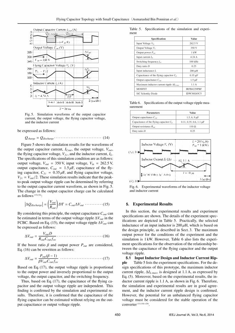
Fig. 5. Simulation waveforms of the output capacitorcurrent, the output voltage, the flying capacitor voltage,and the inductor current
be expressed as follows:
Qcharge = Qdischarge · · · · · · · · · · · · · · · · · · · · · · · · · · · · · (14)
Figure 5 shows the simulation results for the waveforms ofthe output capacitor current, ICout, the output voltage, Vout,the flying capacitor voltage, Vf c, and the inductor current, IL.The specifications of this simulation condition are as follows:output voltage, Vout = 350 V, input voltage, Vin = 262.5 V,output capacitance, Cout = 1.5 μF, capacitance of the fly-ing capacitor, C f c = 0.35 μF, and flying capacitor voltage,Vf c = Vout/2. These simulation results indicate that the peak-to-peak output voltage ripple can be determined by referringto the output capacitor current waveform, as shown in Fig. 5.The change in the output capacitor charge can be calculatedas follows (15) (16):
∣∣∣ΔQdischarge
∣∣∣ =(Vout
Rout
)DT = CoutΔVout · · · · · · · · · · · (15)
By considering this principle, the output capacitance Cout canbe estimated in terms of the output voltage ripple ΔVout in theFCBC. Based on Eq. (15), the output voltage ripple ΔVout canbe expressed as follows:
ΔVout =VoutD
RoutCout fsw· · · · · · · · · · · · · · · · · · · · · · · · · · · · (16)
If the boost ratio β and output power Pout are considered,Eq. (16) can be rewritten as follows:
ΔVout =Pout(β − 1)βVoutCout fsw
· · · · · · · · · · · · · · · · · · · · · · · · · · (17)
Based on Eq. (17), the output voltage ripple is proportionalto the output power and inversely proportional to the outputvoltage, the output capacitor, and the switching frequency.
Thus, based on Eq. (17), the capacitance of the flying ca-pacitor and the output voltage ripple are independent. Thisfinding is confirmed by the simulation and experimental re-sults. Therefore, it is confirmed that the capacitance of theflying capacitor can be estimated without relying on the out-put capacitance or output voltage ripple.
Table 5. Specifications of the simulation and experi-ment
Table 6. Specifications of the output voltage ripple mea-surement
Fig. 6. Experimental waveforms of the inductor voltageand inductor current
5. Experimental Results
In this section, the experimental results and experimentspecifications are shown. The details of the experiment spec-ifications are depicted in Table 5. Practically, the selectedinductance of an input inductor is 200 μH, which is based onthe design principle, as described in Sect. 3. The maximumoutput power for the conditions of the experiment and thesimulation is 1 kW. However, Table 6 also lists the experi-ment specifications for the observation of the relationship be-tween the capacitance of the flying capacitor and the outputvoltage ripple.5.1 Input Inductor Design and Inductor Current Rip-
ple Table 5 lists the experiment specifications. For the de-sign specifications of this prototype, the maximum inductorcurrent ripple, ΔIL-max, is designed at 1.1 A, as expressed byEq. (5). Moreover, based on the experimental results, the in-ductor current ripple is 1.1 A, as shown in Fig. 6. Therefore,the simulation and experimental results are in good agree-ment, and the inductor current ripple design is confirmed.However, the potential for an unbalanced flying capacitorvoltage must be considered for the stable operation of theconverter (11) (18)–(20).
450 IEEJ Journal IA, Vol.3, No.6, 2014
Flying Capacitor Topology with Small Capacitance(Asmarashid Bin Ponniran et al.)
The inductance and core volume of the input inductor aredesigned by considering the maximum inductor current rip-ple as expressed by Eqs. (5) and (12). Theoretically, if thesame specifications of the inductor design are considered, theconventional boost DC-DC converter requires an inductanceof the input inductor of approximately 800 μH, whereas theFCBC requires an inductance of only approximately 200 μH.Moreover, the copper loss is reduced due to the small induc-tance of the input inductor. Hence, the FCBC needs onlyapproximately 25% and 35% of an inductance and an induc-tor core volume of the input inductor, respectively comparedto the conventional DC-DC boost converter. Therefore, thereductions in the inductance and inductor core volume of theinput inductor are reflected in the reduction of the size andweight of the converter.5.2 Relationship between the Capacitance of the Fly-
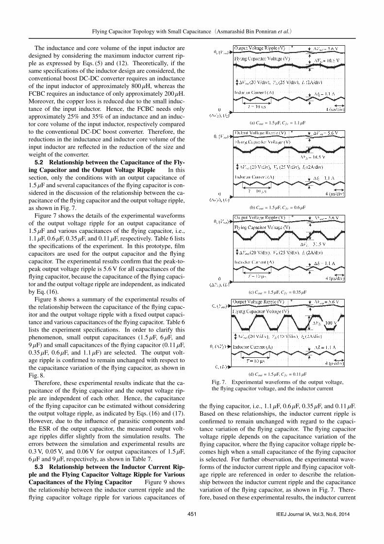
ing Capacitor and the Output Voltage Ripple In thissection, only the conditions with an output capacitance of1.5 μF and several capacitances of the flying capacitor is con-sidered in the discussion of the relationship between the ca-pacitance of the flying capacitor and the output voltage ripple,as shown in Fig. 7.
Figure 7 shows the details of the experimental waveformsof the output voltage ripple for an output capacitance of1.5 μF and various capacitances of the flying capacitor, i.e.,1.1 μF, 0.6 μF, 0.35 μF, and 0.11 μF, respectively. Table 6 liststhe specifications of the experiment. In this prototype, filmcapacitors are used for the output capacitor and the flyingcapacitor. The experimental results confirm that the peak-to-peak output voltage ripple is 5.6 V for all capacitances of theflying capacitor, because the capacitance of the flying capaci-tor and the output voltage ripple are independent, as indicatedby Eq. (16).
Figure 8 shows a summary of the experimental results ofthe relationship between the capacitance of the flying capac-itor and the output voltage ripple with a fixed output capaci-tance and various capacitances of the flying capacitor. Table 6lists the experiment specifications. In order to clarify thisphenomenon, small output capacitances (1.5 μF, 6 μF, and9 μF) and small capacitances of the flying capacitor (0.11 μF,0.35 μF, 0.6 μF, and 1.1 μF) are selected. The output volt-age ripple is confirmed to remain unchanged with respect tothe capacitance variation of the flying capacitor, as shown inFig. 8.
Therefore, these experimental results indicate that the ca-pacitance of the flying capacitor and the output voltage rip-ple are independent of each other. Hence, the capacitanceof the flying capacitor can be estimated without consideringthe output voltage ripple, as indicated by Eqs. (16) and (17).However, due to the influence of parasitic components andthe ESR of the output capacitor, the measured output volt-age ripples differ slightly from the simulation results. Theerrors between the simulation and experimental results are0.3 V, 0.05 V, and 0.06 V for output capacitances of 1.5 μF,6 μF and 9 μF, respectively, as shown in Table 7.5.3 Relationship between the Inductor Current Rip-
ple and the Flying Capacitor Voltage Ripple for VariousCapacitances of the Flying Capacitor Figure 9 showsthe relationship between the inductor current ripple and theflying capacitor voltage ripple for various capacitances of
(a) Cout = 1.5 μF, C f c = 1.1 μF
(b) Cout = 1.5 μF, C f c = 0.6 μF
(c) Cout = 1.5 μF, C f c = 0.35 μF
(d) Cout = 1.5 μF, C f c = 0.11 μF
Fig. 7. Experimental waveforms of the output voltage,the flying capacitor voltage, and the inductor current
the flying capacitor, i.e., 1.1 μF, 0.6 μF, 0.35 μF, and 0.11 μF.Based on these relationships, the inductor current ripple isconfirmed to remain unchanged with regard to the capaci-tance variation of the flying capacitor. The flying capacitorvoltage ripple depends on the capacitance variation of theflying capacitor, where the flying capacitor voltage ripple be-comes high when a small capacitance of the flying capacitoris selected. For further observation, the experimental wave-forms of the inductor current ripple and flying capacitor volt-age ripple are referenced in order to describe the relation-ship between the inductor current ripple and the capacitancevariation of the flying capacitor, as shown in Fig. 7. There-fore, based on these experimental results, the inductor current
451 IEEJ Journal IA, Vol.3, No.6, 2014

Flying Capacitor Topology with Small Capacitance(Asmarashid Bin Ponniran et al.)
Fig. 8. Relationship between the capacitance of the fly-ing capacitor C f c and the output voltage ripple ΔVout
Table 7. Error ratio between the simulation and experi-mental results for the output voltage ripple
Fig. 9. Relationship between the flying capacitor volt-age ripple and the inductor current ripple with the capac-itances of the flying capacitor
ripple and capacitance variation of the flying capacitor are in-dependent of each other. The reason for this condition is thatthe inductor current ripple is dominated by the difference in
Fig. 10. Relationship between the converter efficiencycharacteristics and the capacitance variation of the flyingcapacitor
voltage between the input and output voltages in Mode II, asshown in Fig. 3. As a result, the inductance of an input induc-tor can be estimated without considering the voltage ripple onthe flying capacitor, as described in Sect. 3.5.4 Converter Efficiency for Several Output Power
Levels Figure 10 shows the converter efficiency charac-teristics. Several output power levels are considered for theseexperimental results. The output voltage is fixed at 350 V.Several capacitances of the flying capacitor are consideredfor the efficiency measurement of the constructed prototypecircuit. The achieved maximum efficiency is 98.5% for anoutput power of 1 kW. During this achieved maximum effi-ciency condition, the capacitances of the flying capacitor are1.1 μF and 0.6 μF. Moreover, for the same output power con-dition and a capacitance of the flying capacitor of 0.11 μF,the efficiency is decreased to 98.2% due to the high value ofthe ESR of the capacitor, as compared to that of the otherflying capacitors. Based on these efficiency characteristics,the converter efficiency decreases when the output power isdecreasing, as shown in Fig. 10.5.5 Power Loss Analysis based on Output Power Lev-
els The distribution of the converter power losses is ana-lyzed based on the converter output power. The power lossesare distributed into seven parts, i.e., diode conduction loss,MOSFET conduction loss, MOSFET switching loss, induc-tor copper loss, equivalent series resistance (ESR) loss of theflying capacitor and the output capacitor, no-load loss, andother losses. Moreover, due to the complexity of the esti-mation of the power losses, other losses such as wiring loss,iron loss, and ringing loss are included in the ‘other losses’category, as shown in Fig. 11. In addition, the diode reverse-recovery loss is not considered in the present paper becauseSiC Schottky barrier diodes without reverse-recovery loss areused in the prototype circuit.
Figure 11 shows the details of a power loss distribution ofthe FCBC for several output power levels for a capacitanceof the flying capacitor of 1.1 μF and an output capacitance of6 μF are considered. The total power loss of 100% is based onthe total power loss when the converter power is increased at1 kW. Hence, the total power loss is considered as a referencefor this power loss distribution analysis.
Based on this power loss distribution analysis, one of themajor power losses is dominated by the diode conduction lossfor converter power levels of 1 kW and 800 W. However, it
452 IEEJ Journal IA, Vol.3, No.6, 2014

Flying Capacitor Topology with Small Capacitance(Asmarashid Bin Ponniran et al.)
Fig. 11. Converter loss distribution when the capaci-tance of the flying capacitor is 1.1 μF
was dominated by the ‘other losses’ for a converter powerlevel of 500 W. The inductor copper loss was the lowest com-ponent of the total power loss. Moreover, at output power lev-els of 1 kW and 800 W, ‘other losses’ were the second largestpower losses, followed by the diode conduction loss for aconverter power level of 500 W.
Based on this power loss analysis, the inductor copper lossis small due to smaller number of inductor windings. More-over, MOSFET conduction loss is considered to be small dueto the low input current with regard to the small boost ratio.If the boost ratio is high, the input current becomes high. Asa result, the conduction loss of the MOSFET becomes high.
Since one of the major power losses is associated with thediodes, low-on-voltage diodes must be considered in order toreduce the conduction loss of the diodes. Moreover, the con-duction loss in the flying capacitor is considered to be highdue to the high value of the ESR. Therefore, a low ESR forthe flying capacitors must be selected in order to reduce theflying capacitor conduction loss. In order to reduce the powerloss in the MOSFETs when a high boost ratio is considered,low-on-resistance MOSFETs must be selected. As an option,the on-resistance can be further reduced by connecting theMOSFETs in parallel connection. Therefore, by consideringthese available options, the overall converter efficiency canbe improved further.
6. Conclusion
In the present paper, the authors examined an FCBC witha small-capacitance flying capacitor considering the outputvoltage ripple. Moreover, the authors discussed the analy-sis of the input inductor design. In the present paper, theauthors have discussed (i) the fundamental circuit operationconfirmation of the FCBC, (ii) the design method of an inputinductor, and (iii) the relationship between the capacitance ofthe flying capacitor and the output voltage ripple.
The principal in designing the input inductor in terms ofthe inductance and inductor core volume was explained. Asa result, the inductance and inductor core volume of the in-put inductor were reduced by approximately 25% and 35%,respectively. Moreover, the relationship between the capac-itance of the flying capacitor and the output voltage ripplewas clearly established mathematically and was confirmedby simulation and experimental results. The experimental re-sults confirmed that the capacitance of the flying capacitorand the output voltage ripple are independent of each other.Moreover, the maximum efficiency of the prototype converterwas 98.5% at an output power of 1 kW.
In the future, balancing of the flying capacitor voltage ofthe FCBC will be considered by applying appropriate controlstrategies.
References
( 1 ) H. Keyhani and H.A. Toliyat: “Flying-capacitor boost converter”, in Twenty-Seventh Annual IEEE Applied Power Electronics Conference and Exposition(APEC), 2012 (2012)
( 2 ) Z. Fan, F.Z. Peng, and Q. Zhaoming: “Study of the multilevel converters inDC-DC applications”, in IEEE 35th Annual Power Electronics SpecialistsConference, 2004. PESC 04. 2004 (2004)
( 3 ) Z. Fan, D. Lei, F.Z. Peng, et al.: “A new design method for high efficiencyDC-DC converters with flying capacitor technology”, in Twenty-First An-nual IEEE Applied Power Electronics Conference and Exposition, 2006.APEC’06 (2006)
( 4 ) J. Itoh, K. Matsuura, and K. Orikawa: “Reduction of a boost inductance us-ing a switched capacitor DC-DC converter”, in IEEE 8th International Con-ference on Power Electronics and ECCE Asia (ICPE & ECCE), 2011 (2011)
( 5 ) J. Yungtaek and M.M. Jovanovic: “Interleaved Boost Converter With Intrin-sic Voltage-Doubler Characteristic for Universal-Line PFC Front End”, IEEETransactions on Power Electronics. Vol.22, No.4, pp.1394–1401 (2007)
( 6 ) Z. Junhong, L. Jih-Sheng, K. Rae-young, et al.: “High-Power Density De-sign of a Soft-Switching High-Power Bidirectional dc-dc Converter”, IEEETransactions on Power Electronics, Vol.22, No.4, pp.1145–1153 (2007)
( 7 ) G.V. Torrico-Bascope and I. Barbi: “A single phase PFC 3 kW converter us-ing a three-state switching cell”, in IEEE 35th Annual Power ElectronicsSpecialists Conference, 2004. PESC 04. 2004 (2004)
( 8 ) M. Hirakawa, Y. Watanabe, M. Nagano, et al.: “High power DC/DC con-verter using extreme close-coupled inductors aimed for electric vehicles”, inInternational Power Electronics Conference (IPEC), 2010 (2010)
( 9 ) S.Y. Tseng, J.Z. Shiang, H.H. Chang, et al.: “A Novel Turn-On/Off Snub-ber for Interleaved Boost Converters”, in IEEE Power Electronics SpecialistsConference, 2007. PESC 2007 (2007)
(10) Q. Dongyuan, Z. Bo, and Z. Chunfang: “Duty ratio control of resonantswitched capacitor DC-DC converter”, in Proceedings of the Eighth Interna-tional Conference on Electrical Machines and Systems, 2005. ICEMS 2005(2005)
(11) F.H. Khan and L.M. Tolbert: “A Multilevel Modular Capacitor Clamped DC-DC Converter”, in 41st IAS Annual Meeting Conference Record of the 2006IEEE Industry Applications Conference, 2006 (2006)
(12) O. Keiser, P.K. Steimer, and J.W. Kolar: “High power resonant Switched-Capacitor step-down converter”, in IEEE Power Electronics Specialists Con-ference, 2008. PESC 2008 (2008)
(13) Z. Fan, D. Lei, P.F. Zheng, et al.: “A New Design Method for High-PowerHigh-Efficiency Switched-Capacitor DC-DC Converters”, IEEE Transac-tions on Power Electronics, Vol.23, No.2, pp.832–840 (2008)
(14) M. Shoyama and T. Ninomiya: “Output Voltage Control of Resonant BoostSwitched Capacitor Converter”, in Power Conversion Conference-Nagoya,2007. PCC’07 (2007)
(15) D.W. Hart, Power Electronics 2011, New York: The McGraw-Hill Compa-nies, Inc.
(16 ) N. Mohan, T.M. Undeland, and W.P. Robbins: Power Electronics: Convert-ers, Applications and Design. Vol.3. 2003, United State of America: JohnWiley & Sons, Inc.
(17 ) Wm.T. Mclyman: Transformer and inductor design handbook. 3rd. ed. 2004:Marcel Dekker, Inc.
(18 ) S.H. Hosseini, A.K. Sadig, and A. Sharifi: “Estimation of flying capacitors
453 IEEJ Journal IA, Vol.3, No.6, 2014

Flying Capacitor Topology with Small Capacitance(Asmarashid Bin Ponniran et al.)
voltages in multicell converters”, in 6th International Conference on Elec-trical Engineering/Electronics, Computer, Telecommunications and Informa-tion Technology, 2009. ECTI-CON 2009 (2009)
(19) R. Bensaid and M. Fadel: “Flying capacitor voltages estimation in three-cellconverters using a discrete-time Kalman filter at one third switching period”,in Proceedings of the American Control Conference, 2002 (2002)
(20) G. Gateau, M. Fadel, P. Maussion, et al.: “Multicell converters: active controland observation of flying-capacitor voltages”, IEEE Transactions on Indus-trial Electronics, Vol.49, No.5, pp.998–1008 (2002)
Asmarashid Bin Ponniran (Student Member) received his Bache-lor Degree in Electrical Engineering and Master De-gree in Electrical Engineering (Power) from Univer-siti Tun Hussein Onn Malaysia in 2002 and UniversitiTeknologi Malaysia in 2005, respectively. Presentlyhe is a Ph.D. candidate at Nagaoka University ofTechnology, Japan. At the same time, he is attachedat Universiti Tun Hussein Onn Malaysia, Malaysia asa lecturer. His research interest includes dc-dc con-verter and its application.
Koichi Matsuura (Non-member) received the M.S. degree in electri-cal, electronics and information engineering from Na-gaoka University of Technology, Nagaoka, Japan, in2011. Since 2011, he has been an employee of ToyotaIndustries Corporation. His research interests includeDC-DC converters.
Koji Orikawa (Member) received the M.S. and Ph.D. degrees in elec-trical, electronics and information engineering fromNagaoka University of Technology, Niigata, Japan,in 2010 and 2013 respectively. Since 2013, he hasbeen working at Nagaoka University of Technologyas a postdoctoral fellowship. He is the member ofIEEE and IEEJ. His research interests include powerconversion system especially DC-DC converters andhigh frequency techniques for power converters.
Jun-ichi Itoh (Member) received his M.S. and Ph.D. degrees in elec-trical and electronic systems engineering from Na-gaoka University of Technology, Niigata, Japan in1996 and 2000, respectively. From 1996 to 2004, hewas with Fuji Electric Corporate Research and Devel-opment Ltd., Tokyo, Japan. Since 2004, He has beenwith Nagaoka University of Technology as an asso-ciate professor. He received the IEEJ Academic Pro-motion Award (IEEJ Technical Development Award)in 2007 and the Isao Takahashi Power Electronics
Award in 2010. His research interests include matrix converters, DC/DCconverters, power factor correction techniques and motor drives. He is amember of the Institute of Electrical Engineers of Japan and the Society ofAutomotive Engineers of Japan.
454 IEEJ Journal IA, Vol.3, No.6, 2014