slac -pub-836 a proportional wire chamber … · b. bertolucci, r. carman, j. faust, d. horelick...
TRANSCRIPT

SLAC -PUB-836 A PROPORTIONAL WIRE CHAMBER ELECTRONICS SYSTEM UTILIZING CAMAC* November 1970
B. Bertolucci, R. Carman, J. Faust, D. Horelick (Editor), and J.-L. Pellegrin
Stanford Linear Accelerator Center Stanford University, Stanford, California 94305
Summary
This report describes a system of electronics to be used with a proportional wire chamber hodoscope. The system, which uses CAMAC packaging and data handling philosophy, consists of octo (8 channel) wire signal amplifiers, octo 4-bit per wire latch modules, gate fanout modules, crate control- lers, and two types of data processor-interface units to the SDS 9300 computer. System operation is explained, and each component is described.
Introduction
This report describes a system of electronics to be used with proportional wire chambers which will be installed in the SLAC 20-BeV spectrometer for an experiment in December 1970. In this application the chambers are used as position defining hodoscopes with an externally generated fast gate
&, (% 15-30 nsec) for the electronics. Considerable attention has been given to the timing characteristics of the electronics. Preliminary reports on chamber performance are available. 192
Physical considerations and previous spectrometer oper- ating policies require minimum electronics at the chambers, so the wire amplifiers have been physically separated from the data processing electronics. Amplified wire signals will be transmitted about 400 feet over existing high quality 50R CQaX.
i.’ CAMAC’ packaging and system concepts are used as a convenient method for achieving modularity, flexibility, and ease of expansion, although the more sophisticated aspects of CAMAC are not applicable.
Experimental considerations and processing speed limi- tations require storing of up to 4 independent events per beam pulse, which has a 1.6 psec maximum width, and a maximum 360 pps rate. Each channel therefore contains 4 latch flip- flops.
The system includes a data processor as an interface to the SDS 9300 computer which generates wire addresses, in order to reduce data flow and produce data in a more conven- ient, preprocessed form. Although a processor with internal
‘., memory was originally proposed for optimum data flow, a simpler “scan-stop-read” scanner was built as an interim unit due to schedule considerations. Both units have been built and tested and will be described.
System test facilities are built into the chambers, so that an entire chamber can be pulsed, read out, and verified.
For the initial installation it is planned to have 5 cham- bers, with about 400 total active wires.
System Description and Operation
The overall block diagram of the wire chamber elec - tronics is shown in Fig. 1. Plug-m cards located at the chamber contain amplifiers which raise the wire signals to a -700 mV level for direct transmission over existing Foam-8 cables to the Counting House where latch units, processor, computer, the fast trigger logic, etc. are located. Since the signals are already on coax cables, the additional delays which are normally needed for proportional wire chamber
*Work supported by U.S. Atomic Energy Commission.
signals are externally inserted with coax cables, thereby eliminating the need for any delays in the electronic circuits.
Digital storage (latching) of the chamber signals takes place in the octo-$-bit latch module. Each latch unit accepts 4 NIM fast logic gates each of which is fanned out from a 16- fold fanout unit. The readout system accepts up to 16 latch modules in a crate; a design decision based upon crate power considerations, readout word format, and chamber size. The data is read out onto the CAMAC Read lines in a-bit words, 4 per module, in order to minimize readout circuits in the module. CAMAC standards (EUR 4100e) are followed quite closely inside the crate.
Up to 8 crates are tied together via simplified crate con- trollers and a much simplified branch highway which contains only 8 data lines, 3 crate address lines, 4 module address lines, 2 event lines (subaddress), a clear line and the 52 strobe line. In general, the crate controller and branch high- way are not in accordance with the proposed branch highway specification EUR 4600e, although many of the concepts are similar. The readout philosophy is quite simple: the address is placed on the branch highway, and the returning data is read (strobed) at the last moment, i.e. , just before the address is changed again. This allows maximum settling time of the lines. In our system we have scanned success- fully at a 2 MHz rate.
The scanner interfaces the branch highway to the com- puter I/O and contains sequential addressing and processing logic to generate 2 wire addresses in a 24-bit computer word (see Fig. 2). After reading the word the computer acknowl- edges, and the scanner resumes until the next 2 addresses are found. During scanning, the computer is held by a “not ready” signal. The scanner scans the a-bit words at a 2 MHz rate, so that the maximum scanning time for 4 events, 8 crates, with 128 modules, is 256 psec, in addition to the computer input time.
The memory processor, which is an alternate to the scanner described above, generates two wire addresses per 24-bit word just as in the scanner, but scanning is done off- line and addresses are stored in a 63 word memory. At the end of scanning,the computer is interrupted and the data is read in at a rate limited only by the computer I/O capability. An identification word preceding the data (see Fig. 2) gives the number of wires hit (half-word count) to set up a software read-in table. Since the scanning is off-line, the scan rate is not critical: the selected scan rate of 500 kHz results in a maximum scan time of 1 millisec, well under the SLAC beam spacing of 2.78 millisec.
The basic operating sequence is described as follows. During the beam pulse the trigger logic sends gate signals which strobe data into the latches; after the beam pulse the scanner (processor) is started and subsequently sends wire addresses to the computer. After the data has been sent the scanner (processor) is reset, the latches are reset, and the system is ready to take data from the next beam pulse.
High Speed Electronics
Amplifier
The amplifiers are of conventional design using MC1035 IC ‘s, and are packaged 8 channels on a card which plugs into connectors mounted on the chamber. The overall gain is nominally 600 and the output limits at about -700 mV into 50%
-l-
(Presented at the IEEE 1970 Nuclear Science Symposium, New York City, November 4-6, 1970)

The output, specifically at the request of the experimenters, contains no shapers or standardizing circuitry.
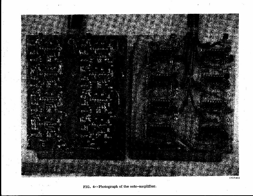
The schematic of the amplifier is shown in Fig. 3 and a photograph in Fig. 4. Special efforts in board layout were made to minimize input wire lengths and channel coupling.
Fanouts
The fanout units are constructed in a single width CAMAC module using conventional circuits and MECL II IC’s. A partial schematic for 4 outputs is shown in Fig. 5. Each fsn- out handles 1 event gate and can drive up to 16 latch module gate inputs in the crate. The unit is dc coupled and has out- put rise and fall times in the order of 5 nsec, which is ade- quate for the 15-30 nsec gate widths.
A photograph of the unit is shown in Fig. 6. Note that Sealectro Snap-on connectors have been used wherever pos- sible, instead of the standard LEMO connector, for space and cost considerations. The module uses only -6 V power and draws about 350 mA.
Otto-4-Bit Latch
This single width module contains 8 identical channels, each with a storage capacity of four bits. Four 50 R gate inputs accept the NIM fast gates which sequentially strobe the 8 inputs. A block diagram of the unit is shown in Fig. 7, and a detailed schematic of a single channel in Fig. 8. Each channel consists of a MC1035, differential receiver- discriminator stage which switches at -300 mV and stan- dardizes the signals from the wire amplifiers into an 8 nsec MEC L level pulse. Thirty-two latch flip-flops consisting of cross-coupled MC1010 gates store the signals after &robing with the event gates. The flip-flop outputs are individually gated onto an 8 bit MECL emitter OR bus which is translated to TTL open collector output levels for the CAMAC read lines. Each 8 bits of readout represents storage of one event in the module. CAMAC addressing is employed: this includes the station line N, and the subaddress lines Al and A2 for the 4 events. Although multiple function codes are not used in this system, the module includes a gate for F(O), Read, so that the module can be used in other more complex systems in the future. The address logic uses one 5 input NAND gate for the F(O), and a Signetics N8251B decoder for the address decoding, the levels of which are translated to MECL to operate the read gates. The latch reset requires an “AND” of Clear and S2, as recommended in CAMAC.
Timing performance of the channel is shown in Fig. 9 which shows gate efficiency for a 15 nsec gate as a function of relative signal and gate timing. It should be pointed out that these measurements were made with 1 nsec time resolution so that the curves are somewhat coarse and only give an indication of the noise and stability of the latch module circuits.
In addition, channel-to-channel variations in nominal gate times occur due to circuit delay differences, layout effects, and differences in circuit thresholds, and give a further indi- cation of the performance. Measurements performed on a single latch module showed timing differences of approximately 1 nsec.
The module uses about 1.1 amps at -6 V and less than 100 mA at +6 V; both voltages are dropped to the proper IC voltages in the module.
The photograph of the module is shown in Fig. 10. Again careful consideration is given to minimum input wire lengths and uniform layout,
Data Handling Electronics
Crate Controller
A minimum nonstandard crate controller was designed especially for this application which is justified by the number of units (up to 8) to be built. However, the branch highway served by the crate controllers employs some of the princi- ples of the proposed standard CAMAC highway.
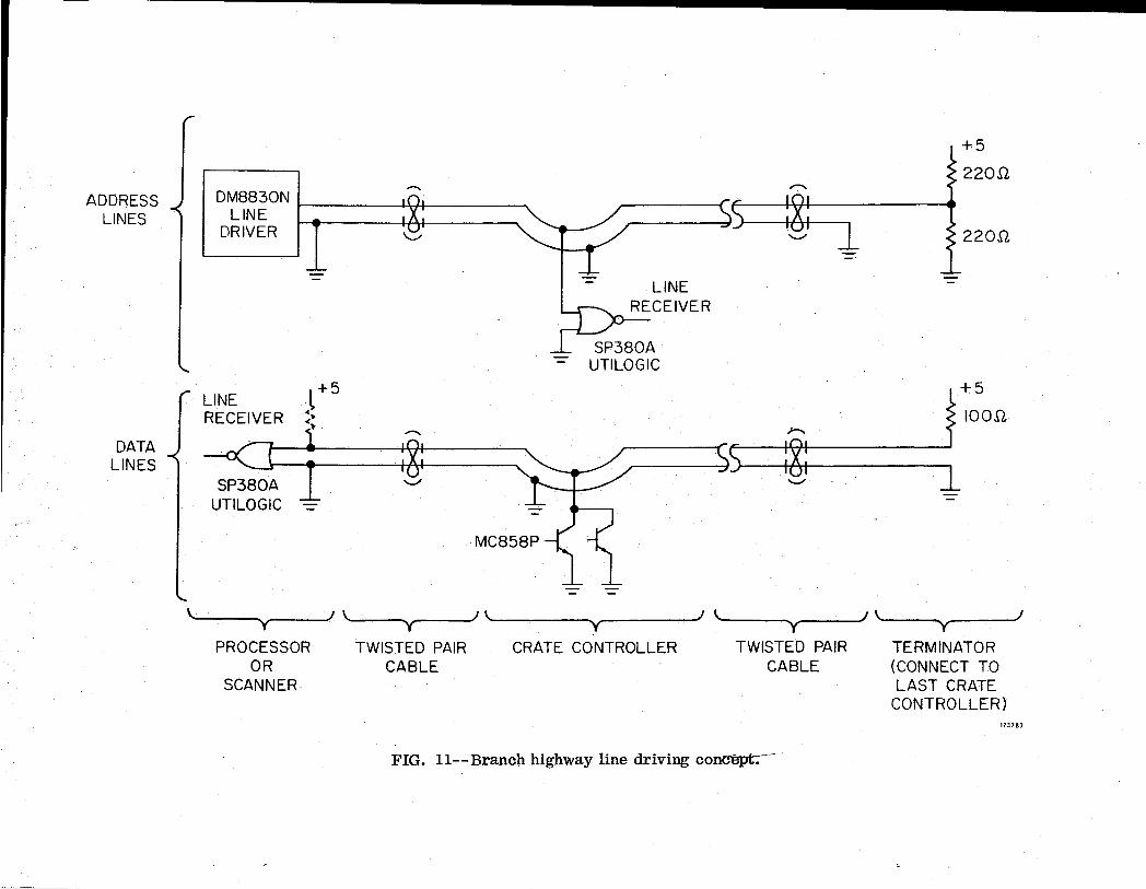
The details of the branch highway twisted-pair line driving are shown in Fig. 11. The address, Clear and S2 lines are driven by the National DM8830N line driver selected for its ability to drive low line impedances. Dual termina- tions to +5 V and ground are placed in a termination unit at the far end of the line4 for optimum termination, although initial tests of the system have shown that such a termination is not required since the branch highway is relatively short (lo’-20’) ; Signals are received in the controllers by the Signetics SP380A Utilogic circuit, which has a high switching threshold (x 1.9 V) and at the same time very light input loading, so that transmission approaches the simplified ideal case. The 8 data lines in the highway are driven in each con- troller by paralleled MC858P open-collector circuits capable of sinking 72 mA nominal at ground. Line terminators to +5 V are located in the processor and/or the line terminator. At the present time 100 R (50 mA) data line pull-up resistors in the 2 MHz scanner have proven adequate, whereas 220 fl pull-up resistors have been used in the processor which scans at 500 kHz.
A block diagram of the crate controller is shown in Fig. 12. The crate number is manually set on a thumbwheel. A comparison circuit energizes the subaddress, station lines, and data outputs when the selected crate address is recog- nized. Gating of the data lines is not logically necessary, but guards against a faulty module in a crate affecting the rest of the system. Note that no timing or module response signals are used in the unit. Pull-up resistors are added to the CAMAC Dataway lines in accordance with the CAMAC specification.
As shown in the photograph (Fig. 13) two branch highway connectors are included which are directly bussed to each other. Mechanical construction is straightforward with the smaller second board in the Normal CAMAC station floating to facilitate alignment. The crate controller contains 13 X’s and draws about 300 mA at +6 V.
Scanner
The scanner drives the branch highway, receives the data, and processes it into 24-bit wordbfor the SDS 9300 computer. The unit, shown in Fig. 14, is constructed in con- ventional chassis form with about 70 TTL IC’s connected by wire-wrap.
The heart of the unit is the g-bit address counter shown in the block diagram, Fig. 15. This synchronous counter sequentially scans the modules at a 2 MHz rate while the scanner tests for l’s in the a-bit data stream with a strobed OR gate. When a “1” is detected, the address scanning stops and the 8 data bits are then scanned at 4 MHz by an 8 to 1 line multiplexer. For each “1” found, the complete la-bit address is stored in one-half of a 24-bit register and the half-word counter is incremented by 1. When the 24-bit word is full, the wire scan stops and the computer reads the data word, after which the wire scan resumes. If there are no more ‘ones” in the a-bit data set then the system reverts to the 2 MHz module scan. This continues until the scan is complete (End of wires), or until the half-word counter reaches 128 (Overflow),after which the half-word count is sent. Then the computer is signalled on the skip bus that the readout is complete. Resetting of the scanner and/or latches may be automatic or external as desired.
-2-

The scanner contains two thumbwheels to limit the extent of the scan and thereby reduce overall scan time. These permit setting of the last crate (O-7) and the last event (O-3) D
Memory Processor
The memory processor is constructed on wire-wrap cards which plug into a commercial wire-wrap chassis (see Fig. 16), and is based upon the use of InteI Corp. 3101 g-bit x Is-word semiconductor memory chips organized into a 64-word, 24-bit high speed read-write memory. The memory is split into two 12-bit halves for purposes of writing half words, but is read out in 24-bit words.
The block diagram is shown in Fig. 17. Operation is quite straightforward, and is somewhat similar to the scan- ner described above. An address generator produces sequential O-bit addresses for the branch highway, and as the 8 bits of data return they are &robed and stored in a register which is continuously scanned by a multiplexer at a 4 MHz rate. The full la-bit word addresses are continu- ously applied to the memory data input lines. When a “1” is found a write enable is sent to the next half of the memory bank to store the wire address at successive memory loca- tions . Note that the wire address comes from a delayed address register which is required since the data in the data register is out of phase with the branch highway address counter by one full module data word. A separate memory address counter and control system keeps track of the cur- rent memory location, memory overflow, and terminates writing after memory overflow. The same memory address counter is used in the readout cycle.
During readout,the identification word, which precedes the data set (see Fig. 2)) is read from a separate register through multiplexer gates into the output. Then the memory is sequentially read out. After the last data word a full word of zeroes is read out as a further check on computer- processor synchronization.
As in the scanner, the memory processor contains thumbwheels to limit the scan to the desired number of crates and events.
The memory processor will not reach its full potential until the computer read-in rate is considerably increased, since the rate is now computer I/O limited to about 30 psec per word.
Crates and Power Supplies
It should be pointed out that the system is not limited to the processing*teohnique described in this report. FQr
example, direct read-in with data packaged as 3-8 bit data words per 24-bit computer word may be accomplished by substituting another interface between the branch highway and the computer port.
To a large extent the system approach described here is a direct result of the SLAC accelerator characteristics of low rate and low duty cycle, which allows considerable time for data processing between beam pulses.
Acknowledgements
This equipment was designed and built by the SLAC Electronics Instrumentation Group headed by R. Larsen, at the request of the SLAC Physics Group A under R. Taylor. E. Bloom and R. Siemann made useful suggestions on the high speed electronics and the overall system.
The authors wish to thank L. Cottrell and W. Graves for their help in defining the scanner, processor, and computer interface characteristics.
Development and construction of the electronics was assisted by P. Arechiga, F. Rosche, R. Partelow, and packaging of the scanner and processor was accomplished by W. Knapp. Special thanks go to R. Hettel who did most of the design detail on the memory processor. Production of the printed circuit boards and modules was handled by the Electronics Shop at SLAC.
References
1. E. Bloom g a&, “Multiwire proportional chambers, ” Report No. SLAC-TN-70-5, Stanford Linear Accelerator Center (March 1970).
2. E. BloometG*, “Multiwire proportional chambers, ” Internal Memorandum, Stanford Linear Accelerator Center (October 27, 1970).
3. CAMAC, A Modular Instrumentation System for Data Handling, Report No. EUR 4100e, EURATOM (March 1969).
4. Abdel-Latif, Strutt, A New Integrated Gate Eliminating Line Reflections in High-Speed Digital Systems, Proceedings of IEEE, June 1970, pp. 936-938.
Standard CAMAC crates, 24 position, manufactured by Nuclear Enterprises, Inc., are being used for this system; each is presently powered by custom packaged Lambda half- rack supplies, -6 V at 30 A, and +6 V at 10 A. A full crate of latch modules, fanouts, and controller draws approxi- mately 18 A at -6 V and approximately 1.4 A at +6 V. Although forced circulation is planned, the modules show minimal temperature rise without it, due to the front entry convention cooling provided by the Nuclear Enterprises crate. Figure 18 shows a photograph of the crate and power supply.
Because of the low power drain on the +6 V supply, it now appears that a more optimum arrangement would be dual 6 V, 30 A supplies, with one supply devoted to all the t6 V power for the system. In this way 5 crates,for example,csn be powered with 3 power supply chassis instead of 5. It is expected to make this packaging change in the near future in order to save valuable space and to standardize on supplies.
Conclusion
We have described a proportional wire chamber elec- tronics system built around CAMAC for convenience and flexibility.
-3-
I

LONG HAUL COAX CABLES
t : :
OCTO LATCH
EVENT STROBES
-
4 - PARALLEL PROCESSOR INPUT
lol CRATE 24 BIT * MULTIPLEXER CONTROLLER DATA WORD I
EVENT START (2 WIRES/WORD) ; ;;;p”u3T”E$
I STROBES I
UP TO 16 OCTO 4 FANOUTS LATCH MODULES PER CRATE PER CRATE
.
. I TO
“BRANCH HIGHWAY”
LATCH = I
8 BITS DATA MODULES : i 9 BITS ADDRESS
I 2 BITS ‘CLEAR LATCHES
UP TO’ 8 CRATES IN SYSTEM
FIG. l--Proportional wire chamber electronics - overall block diagram.

2‘
02 lN
3A3

R2 1.2 K - 0.95ov
INPUT
-I
MC 1035
c----------- ---- -11
rl < OUTPUT
If-
0
- 700mV
RI l.2K 1;;
.2\
R6 2K
025 - 5.2v NOTE:
QI, Q2: 2N3563 J -5.2V 11,711
FIG. 3--Amplifier circuit diagram.

R25
I 68OC QI 2N2905A
r----- 1 I Q3 OUTPUTS
A6 _ ” LJ-
ov R9
-y 270Q -700
il
--A
/4 MCIOIOP ; 3-E-l III
I-+ 14- -i I
T I- I ,-
90!2i I + ; MCIOIOP 1 L------I
k RI2
Lr u Lr
mV
I v
REPEAT FOUR TIMES NOTE: QS-Q6: 2N709 1737Cll
FIG. 5--Fanout circuit diagram.

I

2acJ-J zi’-W
aaz "07

Coincidence Gates -0.75v
-1.55J-f { i-
?PlN 7
7
l I-5.2V
k&v- T-
Input
--JZit
PIN 9
‘-----1
* Line Receiver (Gain=l) ,Discriminator, Differentiator
MC 1035
J--l----V- Quadruple Coincidence Gate Four Bit Latch Quadruple Read Gate
MC 1010 MC 1010 (ileach) MC 1010
FIG. S-Circuit diagram of single channel of o&o-4 bit latch.
Output Data
to MECL - TTL Level Shifter

(‘A) NO
ISSI W SN
VU
c .rl

I
1737A15
ADDRESS LINES
DATA LINES
+5
22oa r? A
DM883ON L 101 PF InI 1) LINE \\
DRIVER v l”, v 22on
- -. - =
LINE
- UTILOGIC
LINE I +5 +5
RECEIVER :; iooa
1 A A InI c- IRI
- I()’ >> IUI SP380A u V
UTILOGIC Y
PROCESSOR OR
SCANNER
TWISTED PAIR CRATE CONTROLLER TWISTED PAIR TERMINATOR CABLE CABLE (CONNECT TO
LAST CRATE CONTROLLER)
FIG. 11--Branch highway line driving conct$t7

CAMAC CRATE
RI r I
BRANCH l-l IGHWAY
R2
R8
1 7-j Ddi.%?S
ENABLE
NI - . . . - LINE . DECODER __ RECEIVER
Nl6- .
I
CRATE NUMBER
THUMB - COMPARE - LINE WHEEL - RECEIVER
Al - - LINE
DRIVERS - RECEIVER A2 -
CLEAR - - 0 DRIVERS LINE
s2p RECEIVER
b
I I
-
C S2 SUBADDRESS CRATE
UNCTION~++S”
STATION ‘(EVENT) ADDRESS NUMBER
L
8 DATA LINES
LINES - Y J
- BRANCH HIGHWAY 1737w
*....a
FIG. 12--Crate controller block diagram.
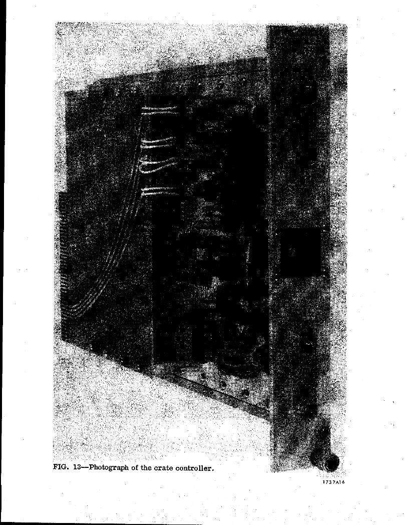
FIG* 13--Photograph of the crate controller.
1737~16


BRANCH HIGHWAY
DATA 8 BITS -1 WIRFS HIT HALt WORD
T * GENt RATOR
1-Y 4-l I 3 ““s I-T- 1 OR GATE TO !-i---T I ^P .L- I I I I I ,.I I
ENABLE -c-
1 r iTART. END OF
CYCLE
DETECT”I:, S Z” WIKtS El
b. COUNTE-R OF 8 8
5, 0s
7BITS ADDRESS
GENERAfOR * 2 MHz t
GATED -- END OF
- 24 BIT CLOCK _
y 03 ro z! IA
e WIRES -
n&. 4 MHz t cln~oJ$
p REGISTER ,p”pj”>
w b F
‘cn U-J 9 BITS ,
L
9 BITS ADDRESS C-p
s2
%EPR I
fl
4 RSDV
J8 2 750nsec
24 DATA
AFTER START H,W.C.
7 r+8
SKS ;SKS GENERATOR.
- INTERNAL RESET
_ RESET - t LATCHES
IO/.& set 1 I-+8
I I 2 100 nsec
NIM/SDSu START EXTE;NAL u
I +8
EXTERNAL RESET
SDS RESET
LATCHES SCANNER
FIG. 15--Scanner block diagram.
SDS 9300


EVENT GATES
16 MULTIPLEXER READ I.D. WRITE - CONTROL
INTERRUPT
READ 4 SYSTEM STEP (RSDV)
RESET - p RESET 24 ‘BIT
X64 WORD COUNTER. L- SOLID STATE
A lWRlTE MEMORY
ENABLE
I I CLEAR AND S2
8 INPUT MUX 8 DATA LINE DATA
REGISTER 8 RECEIVER 8
1
r
DELAYED 9)
LINE ADDRESS
ADDRESS 9 ADDRESS DRIVERS L 9
REGISTER COUNTER
J
TO SDS 9300 COMPUTER
1737c4
FIG. 17--Memory prwessor block diagram.
