sllseh9b –october 2013–revised july 2016 … · v bus d-d+ cc1 gnd vbus_con bus_sys gnd v v out...
TRANSCRIPT

+
VBUS
D-
D+
CC1
GND
VBUS_CON VBUS_SYS
GND
VBUS VOUT
D-
D+
Battery
EN
ACK
VCC
GPIO
GPIO
TPD1S414
TPD4E110
USB Type C Connector
PMIC
System Load
BAT1 µF 2.2 µF
CC2
CC Logic & Port Controller
I2C/GPIO
Copyright © 2016, Texas Instruments Incorporated
Product
Folder
Sample &Buy
Technical
Documents
Tools &
Software
Support &Community
An IMPORTANT NOTICE at the end of this data sheet addresses availability, warranty, changes, use in safety-critical applications,intellectual property matters and other important disclaimers. PRODUCTION DATA.
TPD1S414SLLSEH9B –OCTOBER 2013–REVISED JULY 2016
TPD1S414 USB Charger Overvoltage, Surge, and ESD Protection for VBUS Pin
1
1 Features1• Overvoltage Protection at VBUS_CON Up to 30-V
DC• Low RON nFET Switch Supports Host and
Charging Mode• Internal 15-ms Start-Up Delay• Internal 30-ms Soft-Start Delay to Minimize the
USB Inrush Current• Transient Protection for VBUS Line:
– IEC 61000-4-2 Contact Discharge ±15 kV– IEC 61000-4-2 Air Gap Discharge ±15 kV– IEC 61000-4-5 Open-Circuit Voltage 100 V
• Integrated Input Enable and Status Output Signal• Thermal Shutdown (TSD) Feature• Space-Saving DSBGA Package: (1.4 mm × 1.89
mm)
2 Applications• End Equipment
– Mobile Phones– Tablets– Wearables– Electronic-Point-of-Sale (EPOS)
• Interfaces– USB 2.0– USB 3.0– USB Type C
3 DescriptionThe TPD1S414 device is a single-chip solution for aUSB connector’s VBUS line protection. Thebidirectional nFET switch ensures safe current flow inboth charging and host mode while protecting theinternal system circuits from any overvoltageconditions at the VBUS_CON pin. On the VBUS_CON pin,this device can handle overvoltage protection up to30 V. After the EN pin toggles low, the TPD1S414waits 20 ms before turning ON the nFET through asoft-start delay. ACK pin indicates the FET iscompletely turned ON.
The typical application interface for the TPD1S414 isthe VBUS line in USB connectors. Typical endequipment for TPD1S414 are mobiles phones,tablets, wearables, and electronic-point-of-sale(EPOS). The TPD1S414 can also be applied to anysystem using an interface with a 5-V power rail.
Device Information(1)
PART NUMBER PACKAGE BODY SIZE (NOM)TPD1S414 DSBGA (12) 1.40 mm × 1.89 mm
(1) For all available packages, see the orderable addendum atthe end of the data sheet.
Typical Application Schematic

2
TPD1S414SLLSEH9B –OCTOBER 2013–REVISED JULY 2016 www.ti.com
Product Folder Links: TPD1S414
Submit Documentation Feedback Copyright © 2013–2016, Texas Instruments Incorporated
Table of Contents1 Features .................................................................. 12 Applications ........................................................... 13 Description ............................................................. 14 Revision History..................................................... 25 Pin Configuration and Functions ......................... 36 Specifications......................................................... 4
6.1 Absolute Maximum Ratings ..................................... 46.2 ESD Ratings.............................................................. 46.3 Recommended Operating Conditions....................... 46.4 Thermal Information .................................................. 56.5 Electrical Characteristics (EN, ACK Pins)................. 56.6 Electrical Characteristics (OVP Circuit) .................... 56.7 Timing Requirements ................................................ 66.8 Switching Characteristics (nFET).............................. 66.9 Supply Current Consumption.................................... 66.10 Thermal Shutdown Feature .................................... 66.11 Typical Characteristics ............................................ 8
7 Detailed Description ............................................ 10
7.1 Overview ................................................................. 107.2 Functional Block Diagram ....................................... 107.3 Feature Description................................................. 107.4 Device Functional Modes........................................ 11
8 Application and Implementation ........................ 138.1 Application Information............................................ 138.2 Typical Application ................................................. 13
9 Power Supply Recommendations ...................... 1510 Layout................................................................... 15
10.1 Layout Guidelines ................................................. 1510.2 Layout Example .................................................... 15
11 Device and Documentation Support ................. 1611.1 Receiving Notification of Documentation Updates 1611.2 Community Resource............................................ 1611.3 Trademarks ........................................................... 1611.4 Electrostatic Discharge Caution............................ 1611.5 Glossary ................................................................ 16
12 Mechanical, Packaging, and OrderableInformation ........................................................... 16
4 Revision HistoryNOTE: Page numbers for previous revisions may differ from page numbers in the current version.
Changes from Revision A (October 2013) to Revision B Page
• Added ESD Ratings table, Detailed Description section, Application and Implementation section, Power SupplyRecommendations section, Device and Documentation Support section, and Mechanical, Packaging, and OrderableInformation section ................................................................................................................................................................. 1
Changes from Original (October 2013) to Revision A Page
• Changed text in the DESCRIPTION From: TPD1S414 waits 15 ms before turning ON the nFET To: TPD1S414waits 20 ms before turning ON the nFET............................................................................................................................... 1
• Deleted Continuous forward current through the FET body diode, IDIODE from the ABSOLUTE MAXIMUM RATINGStable ........................................................................................................................................................................................ 4
• Deleted Peak input current on VBUS_CON pin, IBUS from the ABSOLUTE MAXIMUM RATINGS table.................................... 4• Added Voltage on ACK pin to the ABSOLUTE MAXIMUM RATINGS table.......................................................................... 4• Added Continuous current on VBUS_CON and VBUS_SYS pins to the RECOMMENDED OPERATING CONDITIONS table ..... 4• Added Continuous forward current through the FET body diode, IDIODE to the RECOMMENDED OPERATING
CONDITIONS table ................................................................................................................................................................ 4• Added values to the THERMAL INFORMATION table .......................................................................................................... 5• Changed the IHOST_LEAK MAX value From: 160 To: 200 µA in the SUPPLY CURRENT CONSUMPTION table ................... 6• Deleted graphs: Enabling the Load Switch, Connecting VBUS_CON, and OVP Operation from the TIMING DIAGRAMS
section .................................................................................................................................................................................... 7• Changed horizontal axis labeling on Figure 7 ........................................................................................................................ 8• Changed Figure 10............................................................................................................................................................... 14• Added text to the APPLICATION INFORMATION section................................................................................................... 14
GND GND
GND
GND
VBUS_SYS VBUS_SYS
VBUS_SYS VBUS_CON
VBUS_CON VBUS_CON
ACK
EN
3
TPD1S414www.ti.com SLLSEH9B –OCTOBER 2013–REVISED JULY 2016
Product Folder Links: TPD1S414
Submit Documentation FeedbackCopyright © 2013–2016, Texas Instruments Incorporated
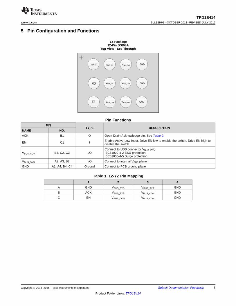
5 Pin Configuration and Functions
YZ Package12-Pin DSBGA
Top View - See Through
Pin FunctionsPIN
TYPE DESCRIPTIONNAME NO.ACK B1 O Open-Drain Acknowledge pin. See Table 2.
EN C1 I Enable Active-Low Input. Drive EN low to enable the switch. Drive EN high todisable the switch.
VBUS_CON B3, C2, C3 I/OConnect to USB connector VBUS pin;IEC61000-4-2 ESD protectionIEC61000-4-5 Surge protection
VBUS_SYS A2, A3, B2 I/O Connect to internal VBUS planeGND A1, A4, B4, C4 Ground Connect to PCB ground plane
Table 1. 12-YZ Pin Mapping1 2 3 4
A GND VBUS_SYS VBUS_SYS GNDB ACK VBUS_SYS VBUS_CON GNDC EN VBUS_CON VBUS_CON GND

4
TPD1S414SLLSEH9B –OCTOBER 2013–REVISED JULY 2016 www.ti.com
Product Folder Links: TPD1S414
Submit Documentation Feedback Copyright © 2013–2016, Texas Instruments Incorporated
(1) Stresses beyond those listed under Absolute Maximum Ratings may cause permanent damage to the device. These are stress ratingsonly, which do not imply functional operation of the device at these or any other conditions beyond those indicated under RecommendedOperating Conditions. Exposure to absolute-maximum-rated conditions for extended periods may affect device reliability.
(2) The algebraic convention, whereby the most negative value is a minimum and the most positive value is a maximum.
6 Specifications
6.1 Absolute Maximum Ratingsover operating free-air temperature range (unless otherwise noted) (1) (2)
MIN MAX UNITSupply voltage from USB connector, VBUS_CON –0.3 30 VInternal supply DC voltage rail on the PCB, VBUS_SYS –0.5 7 VVoltage on EN pin –0.5 7 VVoltage on ACK pin –0.5 7 VOutput load capacitance, CLOAD VBUS_SYS pin 0.1 50 µFInput capacitance, CON VBUS_CON pin 0.1 50 µFOperating free-air temperature, TA –40 85 °CStorage temperature, Tstg –40 150 °C
(1) JEDEC document JEP155 states that 500-V HBM allows safe manufacturing with a standard ESD control process. Pins listed as±2000 V may actually have higher performance.
(2) JEDEC document JEP157 states that 250-V CDM allows safe manufacturing with a standard ESD control process. Pins listed as±1000 V may actually have higher performance.
6.2 ESD RatingsVALUE UNIT
V(ESD)Electrostaticdischarge
Human-body model (HBM), per ANSI/ESDA/JEDEC JS-001 (1) ±2000V
Charged-device model (CDM), per JEDEC specification JESD22-C101 (2) ±1000IEC 61000-4-2 contact discharge ±15000 VIEC 61000-4-2 air-gap discharge ±15000 VIEC 61000-4-5 Peak Pulse Current (tp = 8/20 µs) VBUS_CON pin 21 AIEC 61000-4-5 Peak Pulse Power (tp = 8/20 µs) VBUS_CON pin 700 WIEC 61000-4-5 Open circuit voltage (tp = 1.2/50 µs) VBUS_CON pin 100 V
6.3 Recommended Operating Conditionsover operating free-air temperature range (unless otherwise noted)
PARAMETER MIN NOM MAX UNITVBUS_CON Supply voltage from USB connector 5.9 VVBUS_SYS Internal supply DC voltage rail on the PCB 5.9 VCLOAD Output load capacitance VBUS_SYS pin 2.2 µFCIN Input capacitance VBUS_CON pin 1 µFRPULLUP Pullup resistor ACK pin 4.3 100 kΩ
IVBUS Continuous current on VBUS_CON and VBUS_SYS pins VBUS_CONVBUS_SYS
3.5 A
IDIODE Continuous current through the FET body diode 1 A

5
TPD1S414www.ti.com SLLSEH9B –OCTOBER 2013–REVISED JULY 2016
Product Folder Links: TPD1S414
Submit Documentation FeedbackCopyright © 2013–2016, Texas Instruments Incorporated
(1) For more information about traditional and new thermal metrics, see the Semiconductor and IC Package Thermal Metrics applicationreport.
6.4 Thermal Information
THERMAL METRIC (1)TPD1S414
UNITYZ (DSBGA)12 PINS
RθJA Junction-to-ambient thermal resistance 89 °C/WRθJC(top) Junction-to-case(top) thermal resistance 0.6 °C/WRθJB Junction-to-board thermal resistance 16.3 °C/WψJT Junction-to-top characterization parameter 2.7 °C/WψJB Junction-to-board characterization parameter 16.2 °C/WRθJC(bot) Junction-to-case(bottom) thermal resistance n/A °C/W
6.5 Electrical Characteristics (EN, ACK Pins)over operating free-air temperature range (unless otherwise noted)
PARAMETER TEST CONDITIONS MIN TYP MAX UNITVIH High-level input voltage, EN 1.2 6 VVIL Low-level input voltage, EN 0.8 VIIL Input leakage current EN VI = 3.3 V 1 µAVOL Low-level output voltage, ACK IOL = 3 mA 0.4 V
6.6 Electrical Characteristics (OVP Circuit)over operating free-air temperature range (unless otherwise noted)
PARAMETER TEST CONDITIONS MIN TYP MAX UNIT
VOVP_RISINGInput overvoltage protectionthreshold, VBUS_CON
VBUS_CON increasing from 5 V 6 6.2 6.4 V
VHYS_OVP Hysteresis on OVP, VBUS_CONVBUS_CON decreasing from 7 V to5 V 50 mV
VOVP_FALLINGInput overvoltage protectionthreshold, VBUS_CON
VBUS_CON decreasing from 7 V to5 V 5.93 6.37 V
VUVLOInput undervoltage lockout,VBUS_CON
VBUS_CON voltage rising from 0 Vto 5 V 3.1 3.3 3.5 V
VHYS_UVLO Hysteresis on UVLO, VBUS_CONDifference between rising andfalling UVLO thresholds 100 mV
VUVLO_FALLINGInput undervoltage lockout,VBUS_CON
VBUS_CON voltage rising from 5 Vto 0 V 3 3.2 3.4 V
VUVLO_SYSVBUS_SYS undervoltage lockout,VBUS_SYS
VBUS_SYS voltage rising from 0 Vto 5 V 3.1 3.6 4.3 V
VHYS_UVLO_SYSVBUS_SYS UVLO Hysteresis,VBUS_SYS
Difference between rising andfalling UVLO thresholds onVBUS_SYS
480 mV
VUVLO_SYS_FALLVBUS_SYS undervoltage lockout,VBUS_SYS
VBUS_SYS voltage falling from 7 Vto 5 V 3 3.2 3.4 V
6
TPD1S414SLLSEH9B –OCTOBER 2013–REVISED JULY 2016 www.ti.com
Product Folder Links: TPD1S414
Submit Documentation Feedback Copyright © 2013–2016, Texas Instruments Incorporated
(1) Shown in Figure 1.(2) Parameters provided for reference only, and do not constitute part of TI's published device specifications for purposes of TI's product
warranty.(3) Excludes soft-start time
6.7 Timing Requirementsover operating free-air temperature range (unless otherwise noted)
MIN NOM MAX UNIT
tDELAY USB charging turnon delayMeasured from EN asserted LOW tonFET beginning to Turn ON (1)
excluding soft-start time20 ms
tSSUSB charging rise time (soft-startdelay)
Measure from VBUS_SYS rises above25% (with 1-MΩ load/ NO CLOAD) untilACK goes Low (10%)
25 ms
tOFF_DELAY USB charging turnoff timeMeasured from EN asserted High toVBUS_SYS falling to 10% with RLOAD =10 Ω and No CLOAD on VBUS_SYS
4 µs
OVERVOLTAGE PROTECTION
tOVP_response OVP response timeMeasured from OVP Condition to FETTurn OFF (2). VBUS_CON rises at 1V /100 ns
100 ns
tOVP_Recov Recovery time Measured from OVP Clear to FET TurnON (3) 20 ms
6.8 Switching Characteristics (nFET)over operating free-air temperature range (unless otherwise noted)
PARAMETER TEST CONDITIONS MIN TYP MAX UNIT
RDS(on) Switch ON-resistance VBUS_CON = 5 V, IOUT = 1 A,TA = 25˚C 39 50 mΩ
6.9 Supply Current Consumptionover operating free-air temperature range (unless otherwise noted)
PARAMETER TEST CONDITIONS MIN TYP MAX UNIT
IVBUS_SLEEP VBUS_CON operating currentconsumption
Measured at VBUS_CON pin,VBUS_CON = 5 V, EN =5V 30 70 µA
IVBUSMeasured at VBUS_CON pin,VBUS_CON = 5 V, EN 0 V and no load 175 373 µA
IVBUS_SYSVBUS_CON operating currentconsumption
Measured at VBUS_SYS pin,VBUS_SYS = 5 V, EN = 0 V andVBUS_CON = Hi Z
175 373 µA
IHOST_LEAK Host mode leakage currentMeasured at VBUS_SYS,VBUS_CON = Hi Z, EN = 5 V,VBUS_SYS = 5 V
90 200 µA
6.10 Thermal Shutdown Featureover operating free-air temperature range (unless otherwise noted)
PARAMETER TEST CONDITIONS MIN TYP MAX UNIT
TSHDNThermal shutdown Junction temperature 145 °CThermal-shutdown hysteresis Junction temperature 35 °C

VOVP
VBUS_SYS
Overtemperature
Condition
EN
VBUS_CON
tDELAY
tOFF_DELAYtSS
VUVLO
7
TPD1S414www.ti.com SLLSEH9B –OCTOBER 2013–REVISED JULY 2016
Product Folder Links: TPD1S414
Submit Documentation FeedbackCopyright © 2013–2016, Texas Instruments Incorporated
Figure 1. Thermal Shutdown Operation

0.00
0.20
0.40
0.60
0.80
1.00
1.20
1.40
1.60
1.80
2.00
±40 ±20 0 20 40 60 80 100
Nor
mal
ized
TD
ELA
Y
Temperature (�C) C005
0
2
4
6
8
10
12
14
0 200 400 600 800 1000 1200 1400
Vol
tage
(V
)
Time (ns)
VBUS_SYS
VBUS_CON
C006
0.0
0.5
1.0
1.5
2.0
2.5
3.0
0.1 0.6 1.1 1.6 2.1 2.6
Nor
mal
ized
RD
S(O
N)
Output Current (A) C003
0.90
0.95
1.00
1.05
1.10
±40 ±20 0 20 40 60 80 100
Nor
mal
ized
VO
VP
Temperature (�C) C004
0
100
200
300
400
500
600
700
800
0 5 10 15 20 25 30 35
Inpu
t C
urre
nt (
uA)
Input Voltage (V)
T = -30
T = 25
T = 85
C001
TA = t30�C TA = 25�C
TA = 85�C
0.0
0.2
0.4
0.6
0.8
1.0
1.2
1.4
1.6
1.8
2.0
±40 ±20 0 20 40 60 80 100
Nor
mal
ized
RD
S(O
N)
Temperature (�C) C002
8
TPD1S414SLLSEH9B –OCTOBER 2013–REVISED JULY 2016 www.ti.com
Product Folder Links: TPD1S414
Submit Documentation Feedback Copyright © 2013–2016, Texas Instruments Incorporated
6.11 Typical Characteristics
Figure 2. Input Supply Current vs Supply Voltage Figure 3. Normalized RDS(ON) vs Temperature
Figure 4. Normalized RDS(ON) vs Output Current Figure 5. Normalized VOVP
Figure 6. Normalized TDELAY Figure 7. VOVP Response Time
±1
0
1
2
3
4
5
6
±15 ±10 ±5 0 5 10 15 20 25 30 35
Am
plitu
de (
V)
Time (ms)
VBUS_SYS
VBUS_CON
I_VBUS_CON
C007
±5
0
5
10
15
20
25
30
35
40
45
50
±10 0 10 20 30 40 50 60 70 80 90
Vol
tage
(V
) an
d C
urre
nt (
A)
Time (µs)
Vsys (V)
Vcon (V)
Icon (A)
C008
TPD1S414YZ
8/20 Surge Waveforms
100 V (into an open), Powered Down
9
TPD1S414www.ti.com SLLSEH9B –OCTOBER 2013–REVISED JULY 2016
Product Folder Links: TPD1S414
Submit Documentation FeedbackCopyright © 2013–2016, Texas Instruments Incorporated
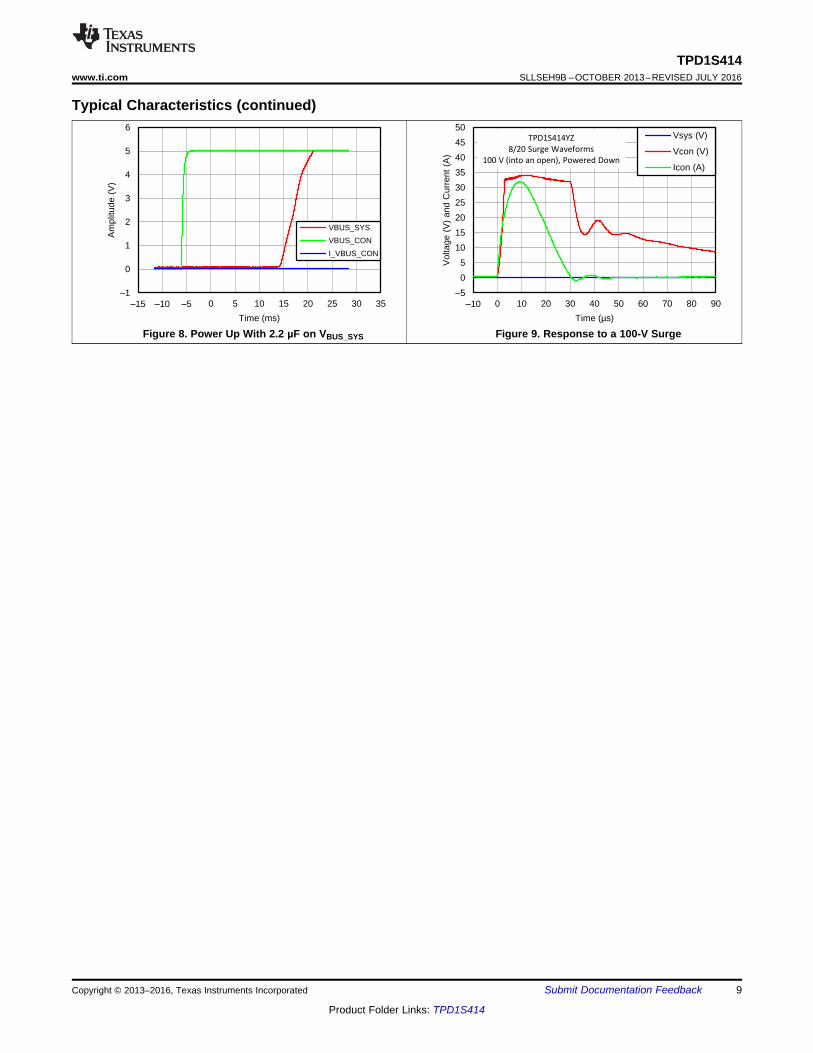
Typical Characteristics (continued)
Figure 8. Power Up With 2.2 µF on VBUS_SYS Figure 9. Response to a 100-V Surge

Internal BandgapReference
Control Logicand Charge
Pump
VBUS_CON
/ACK
/EN
GND
PrecisionSurge
ClampingCircuit
VBUS_SYS
Copyright © 2016, Texas Instruments Incorporated
10
TPD1S414SLLSEH9B –OCTOBER 2013–REVISED JULY 2016 www.ti.com
Product Folder Links: TPD1S414
Submit Documentation Feedback Copyright © 2013–2016, Texas Instruments Incorporated
7 Detailed Description
7.1 OverviewThe TPD1S414 provides a single-chip ESD protection, surge protection, and overvoltage protection solution forportable USB charging and Host interfaces. It offers overvoltage protection at the VBUS_CON pin up to 30 V. TheTPD1S414 also provides a ACK pin that indicates to the system if a fault condition has occurred. The TPD1S414offers an ESD clamp and a surge clamp for VBUS_CON pin, thus eliminating the need for external TVS clampcircuits in the application.
The TPD1S414 has an internal oscillator and charge pump that controls the turnon of the internal nFET switch.The internal oscillator controls the timers that enable the charge pump and resets the open-drain ACK output. IfVBUS_CON is less than VOVP, the internal charge pump is enabled. After a 15-ms internal delay, the charge-pumpstarts up, and turns on the internal nFET switch through a soft start. Once the nFET is completely turned ON,TPD1S414 asserts ACK pin LOW. At any time, if VBUS_CON rises above VOVP, the ACK pin is in High-Z and ispulled HIGH through external resistors. The nFET switch is turned OFF.
7.2 Functional Block Diagram
7.3 Feature Description
7.3.1 Overvoltage Protection on VBUS_CON up to 30-V DCWhen the VBUS_CON voltage rises above VOVP, the internal nFET switch is turned off, removing power from thesystem side. VBUS_CON can tolerate up to 30-V DC. The response to overvoltage is very rapid, with the nFETswitch turning off in less than 100 ns. When the VBUS_CON voltage returns back to below VOVP – VHYS_OVP, thenFET switch is turned on again after an internal delay of tOVP_RECOV (tDELAY). This time delay ensures that theVBUS_CON supply has stabilized before turning the switch back on. After tOVP_RECOV, the TPD1S414 turns on thenFET through a soft start. Once the OVP condition is cleared the nFET is turned completely on.
7.3.2 Low RON nFET Switch Supports Host and Charging ModeThe nFET switch has a total ON-resistance (RON) of 39 mΩ. This equates to a voltage drop of less than 140 mVwhen charging at the maximum 3.5-A current level. Such low RON helps provide maximum potential to thesystem as provided by an external charger or by the system when in host mode.
7.3.3 ±15-kV IEC 61000-4-2 Level 4 ESD ProtectionThe VBUS_CON pin can withstand ESD events up to ±15-kV Contact and Air-Gap. An ESD clamp diverts thecurrent to ground.

11
TPD1S414www.ti.com SLLSEH9B –OCTOBER 2013–REVISED JULY 2016
Product Folder Links: TPD1S414
Submit Documentation FeedbackCopyright © 2013–2016, Texas Instruments Incorporated
Feature Description (continued)7.3.4 100-V IEC 61000-4-5 µs Surge ProtectionThe VBUS_CON pin can withstand surge events up to 100-V open-circuit voltage (VPP), and 700 W. A precisionclamp diverts the current to ground and active circuitry switches OFF the nFET earlier than 100 ns before anovervoltage can get through to VBUS_SYS.
7.3.5 Start-Up and OVP Recovery DelayThe TPD1S414 has a built-in start-up delay. Once the device has been enabled, a time tDELAY elapses before thecharge pump is enabled which turns on the nFET. A manufactured preprogrammed soft start, tSS, is used whenturning on the nFET with the charge pump. Once the device is enabled, these start delays, tDELAY + tSS, worktogether to meet the USB inrush current compliance. Similarly, after an OVP event has occurred, the devicewaits a time tOVP_RECOV before enabling the charge pump to turn on the nFET. The soft-start, tSS, is still usedwhen turning on the nFET with the charge pump after an OVP event, making the total time for the nFET switch toturn on after the OVP event tOVP_RECOV + tSS.
7.3.6 Integrated Input Enable and Status Output SignalThe TPD1S414 integrates an enable signal to control the ON and OFF state of its nFET. The device alsointegrates an status output signal through the ACK pin which indicates whether or not a fault is occurring on thedevice. See the Table 2 table to understand the functionality of these pins in all of the TPD1S414's states.
7.3.7 Thermal ShutdownThe TPD1S414 family has an overtemperature protection circuit to protect against system faults or improper use.The basic function of the thermal shutdown (TSD) circuit is to sense when the junction temperature hasexceeded the absolute maximum rating and shuts down the device until the junction temperature has cooled to asafe level. When in the thermal shutdown condition, the device asserts a fault by setting the ACK pin to High-Z.
7.4 Device Functional Modes
7.4.1 VBUS_CON < VUVLO
When VBUS_CON is less than VUVLO, the device is in its unpowered state. The nFET is OFF and the ACK pin isHigh-Z. In this state, TPD1S414 still provides IEC 61000-4-2 ±15-kV Contact/±15-kV air-gap protection and IEC61000-4-5 100-V open-circuit surge protection.
7.4.2 VUVLO < VBUS_CON < VOVP
When VBUS_CON is greater than VUVLO and less than VOVP, the device is in its powered state. In this state, thenFET can be controlled ON and OFF through the enable pin. When the EN pin is Low, the nFET is ON and canbe used for both charging and host or OTG mode. While the nFET switch is ON, the ACK pin is held Low. Whenthe enable pin is high, the nFET switch is held OFF and the ACK pin is High-Z. In both the enable and disabledstates, the TPD1S414 provides IEC 61000-4-2 ±15-kV contact/±15-kV air-gap protection and IEC 61000-4-5 100-V open-circuit surge protection.
7.4.3 VBUS_CON > VOVP
When VBUS_CON is greater than VOVP, the device is in the overvoltage protection sate. In this state, the nFETswitch is forced OFF regardless of the state of the enable pin and ACK is set High-Z. VBUS_CON can handleovervoltage protection up to 30 V.
7.4.4 OVP OperationWhen the VBUS_CON voltage rises above VOVP, the internal nFET switch is turned off, removing power from thesystem. The response is rapid, with the FET switch turning off in less than 100 ns. The ACK pin is set to High-Zwhen an overvoltage condition is detected and the nFET is turned OFF. This pin can be pulled up throughexternal resistors to indicate an OVP condition. When the VBUS_CON voltage returns below VOVP – VHYS-OVP, thenFET switch is turned on again after the internal delay of tOVP_Recov. This delay time ensures that the VBUS_CONsupply has stabilized before turning the switch back on. After tOVP_Recov, the TPD1S414 turns on the nFETthrough a soft start to ensure that the USB Inrush current compliance is met. When the OVP condition is clearedand the nFET is completely turned on, the ACK is reset LOW.
12
TPD1S414SLLSEH9B –OCTOBER 2013–REVISED JULY 2016 www.ti.com
Product Folder Links: TPD1S414
Submit Documentation Feedback Copyright © 2013–2016, Texas Instruments Incorporated
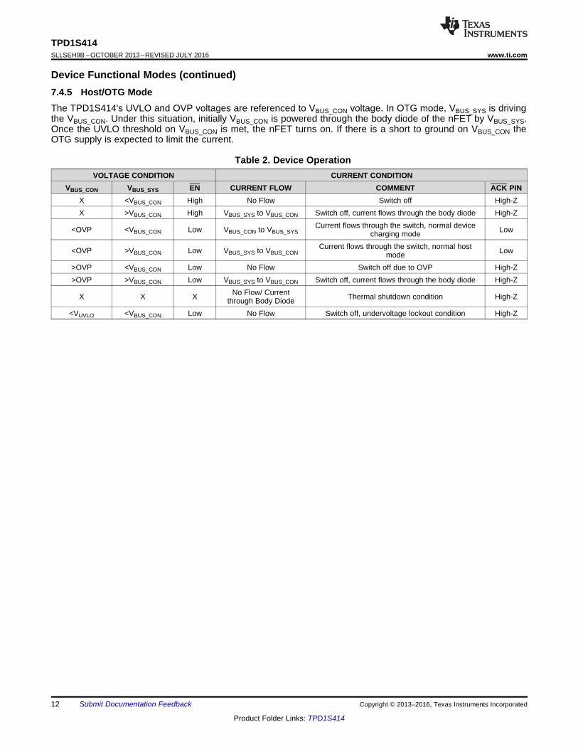
Device Functional Modes (continued)7.4.5 Host/OTG ModeThe TPD1S414's UVLO and OVP voltages are referenced to VBUS_CON voltage. In OTG mode, VBUS_SYS is drivingthe VBUS_CON. Under this situation, initially VBUS_CON is powered through the body diode of the nFET by VBUS_SYS.Once the UVLO threshold on VBUS_CON is met, the nFET turns on. If there is a short to ground on VBUS_CON theOTG supply is expected to limit the current.
Table 2. Device OperationVOLTAGE CONDITION CURRENT CONDITION
VBUS_CON VBUS_SYS EN CURRENT FLOW COMMENT ACK PINX <VBUS_CON High No Flow Switch off High-ZX >VBUS_CON High VBUS_SYS to VBUS_CON Switch off, current flows through the body diode High-Z
<OVP <VBUS_CON Low VBUS_CON to VBUS_SYSCurrent flows through the switch, normal device
charging mode Low
<OVP >VBUS_CON Low VBUS_SYS to VBUS_CONCurrent flows through the switch, normal host
mode Low
>OVP <VBUS_CON Low No Flow Switch off due to OVP High-Z>OVP >VBUS_CON Low VBUS_SYS to VBUS_CON Switch off, current flows through the body diode High-Z
X X X No Flow/ Currentthrough Body Diode Thermal shutdown condition High-Z
<VUVLO <VBUS_CON Low No Flow Switch off, undervoltage lockout condition High-Z
+
VBUS
D-
D+
CC1
GND
VBUS_CON VBUS_SYS
GND
VBUS VOUT
D-
D+
Battery
EN
ACK
VCC
GPIO
GPIO
TPD1S414
TPD4E110
USB Type C Connector
PMIC
System Load
BAT1 µF 2.2 µF
CC2
CC Logic & Port Controller
I2C/GPIO
Copyright © 2016, Texas Instruments Incorporated
13
TPD1S414www.ti.com SLLSEH9B –OCTOBER 2013–REVISED JULY 2016
Product Folder Links: TPD1S414
Submit Documentation FeedbackCopyright © 2013–2016, Texas Instruments Incorporated
8 Application and Implementation
NOTEInformation in the following applications sections is not part of the TI componentspecification, and TI does not warrant its accuracy or completeness. TI’s customers areresponsible for determining suitability of components for their purposes. Customers mustvalidate and test their design implementation to confirm system functionality.
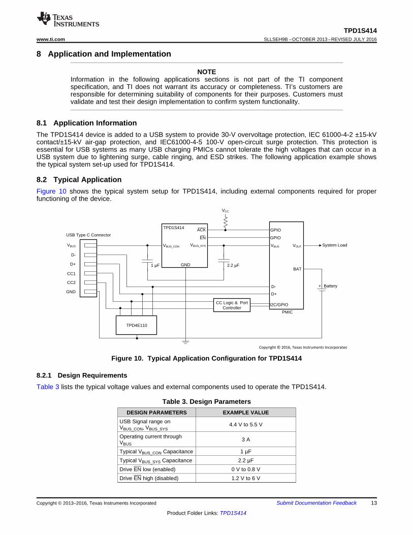
8.1 Application InformationThe TPD1S414 device is added to a USB system to provide 30-V overvoltage protection, IEC 61000-4-2 ±15-kVcontact/±15-kV air-gap protection, and IEC61000-4-5 100-V open-circuit surge protection. This protection isessential for USB systems as many USB charging PMICs cannot tolerate the high voltages that can occur in aUSB system due to lightening surge, cable ringing, and ESD strikes. The following application example showsthe typical system set-up used for TPD1S414.
8.2 Typical ApplicationFigure 10 shows the typical system setup for TPD1S414, including external components required for properfunctioning of the device.
Figure 10. Typical Application Configuration for TPD1S414
8.2.1 Design RequirementsTable 3 lists the typical voltage values and external components used to operate the TPD1S414.
Table 3. Design ParametersDESIGN PARAMETERS EXAMPLE VALUE
USB Signal range onVBUS_CON, VBUS_SYS
4.4 V to 5.5 V
Operating current throughVBUS
3 A
Typical VBUS_CON Capacitance 1 µFTypical VBUS_SYS Capacitance 2.2 µFDrive EN low (enabled) 0 V to 0.8 VDrive EN high (disabled) 1.2 V to 6 V

±5
0
5
10
15
20
25
30
35
40
45
50
±10 0 10 20 30 40 50 60 70 80 90
Vol
tage
(V
) an
d C
urre
nt (
A)
Time (µs)
Vsys (V)
Vcon (V)
Icon (A)
C008
TPD1S414YZ
8/20 Surge Waveforms
100 V (into an open), Powered Down
14
TPD1S414SLLSEH9B –OCTOBER 2013–REVISED JULY 2016 www.ti.com
Product Folder Links: TPD1S414
Submit Documentation Feedback Copyright © 2013–2016, Texas Instruments Incorporated
8.2.2 Detailed Design Procedure
8.2.2.1 USB VBUS Voltage RangeThe USB VBUS voltage range for a USB device operates between a minimum of 4.4 V and a maximum of 5.5 V(Legacy USB has a maximum of 5.25 V, but the new USB Type C standard raised the maximum to 5.5 V). TheTPD1S414 is designed to operate with a VBUS_CON, VBUS_SYS voltage between 3.5 V and 5.9 V. This rangeexceeds the requirements for USB VBUS, allowing this device to be used in any USB system. Therefore, nospecial voltage precautions are necessary when adding TPD1S414 to a USB system.
8.2.2.2 USB VBUS Operating CurrentIn this application example, a VBUS current of 3 A is required. With the addition of the new USB Type C Standard,the VBUS operating current can vary anywhere from 0.5 A to 3 A, depending on the current capability advertisedby the source on the CC pin. TPD1S414 is designed to operate up to a maximum of 3.5 A of current, allowing itto be used with the new USB Type C connector. TPD1S414 also has a low RON of 39 mΩ (typical), 50 mΩ(maximum), allowing for excellent thermal performance and low voltage drop across the switch at 3 A.
8.2.2.3 VBUS_CON and VBUS_SYS CapacitanceThe USB standard requires a minimum capacitance of 1 µF on VBUS and allows for a maximum capacitance of10 µF on a USB device. The minimum capacitance is to reduce inductive spiking on VBUS when disconnectingthe charging cable, and the maximum capacitance is to put a limit on how much a device can drop the VBUS railof its host when being hot-plugged into the system. This corresponds to having a typical capacitance of 1 µF onVBUS_CON for a USB system, but higher capacitance up to 10 µF can be used. No more than 10 µF must be puton VBUS_CON to ensure the USB specification is not violated. If more capacitance is required, place this on theVBUS_SYS pin. TPD1S414 turns on its nFET switch with a soft start to help pass USB in-rush compliance, so it isrecommended to place bulk capacitance on the VBUS_SYS pin. External capacitors added to the VBUS_CON pin mustbe placed as close to the VBUS_CON pin as possible, and likewise external capacitors added to the VBUS_SYS pinmust be placed as close to the VBUS_SYS pin as possible.
8.2.2.4 IEC 61000-4-5 100-V Open-Circuit SurgeThe IEC 61000-4-5 standard specifies the lightning and industrial surge model. Power lines like the VBUS line onthe USB port are subject to switching and lightning transients. Power supply switching transients can enter thesystem due to capacitor bank switching on the rail, minor load switching on the system and various system faultslike arcing to the grounding system of the installation. Direct lightning to the outer installations cause anovervoltage condition on the VBUS line. In the event of an overvoltage condition, the OVP block of the processoror the protection circuitry turns off isolating the system from these transients. Abruptly turning off the load, causesa further ripple due to the inductive nature of the charging cable. End systems require protection against thesetransients. These transients have greater energy than the ESD events. Systems cannot be protected from thesetransients using simple ESD diodes. The TPD1S414 has a precision trigger and precision clamping circuit thatensures a DC tolerance of 30 V while suppressing surge voltage up to 100 V under 35 V. Figure 11 shows theperformance of TPD1S414 in the powered-down state under an 100-V surge pulse.
8.2.3 Application Curve
Figure 11. TPD1S414 Response to an 100-V Surge

EP Gray
GND GND GND
EP Gray
/EN
EP Gray
/ACK
EP Gray
GND
EP Gray
EP
Gray
VBUS_CONVBUS_CON
EP
Gray
VBUS_SVS
EP Gray
VBUS_SVSVBUS_CON
VBUS_SVS
EP
Gray EP Gray
15
TPD1S414www.ti.com SLLSEH9B –OCTOBER 2013–REVISED JULY 2016
Product Folder Links: TPD1S414
Submit Documentation FeedbackCopyright © 2013–2016, Texas Instruments Incorporated
9 Power Supply RecommendationsThe TPD1S414 is designed to receive power from a USB VBUS rail. It can operate normally (nFET ON) betweena minimum of 3.5 V and a maximum of 5.9 V, well exceeding the USB device VBUS voltage range of 4.4 V to5.5 V. Place a capacitor with a minimum capacitance of 1 µF across system voltage range, system temperaturerange, and capacitor variation as close as possible to the VBUS_CON pin on the PCB.
10 Layout
10.1 Layout GuidelinesTPD1S414 can be routed in a single-layer PCB. PCB traces to VBUS_SYS, VBUS_CON, and GND can be routed inthe fashion shown in Figure 12.
Shorting all of the VBUS_SYS pins together, all the VBUS_CON pins together, and all the GND pins together helpsprovide the lowest resistance between the USB connector and the PMIC. For this example, the trace widths toVBUS_SYS, VBUS_CON are 25 mils (0.635 mm) under TPD1S414. There are no VIAs required within the SMD padsin this design. Stitching VIAs for GND can be placed near the component instead.
The decoupling capacitors per the Recommended Operating Conditions must be placed as close as possible tothe TPD1S414. There must be a short path from the device ground pins to the system ground plane. Thisensures best protection under ESD and surge transients.
10.2 Layout Example
Figure 12. TPD1S414 Layout Example

16
TPD1S414SLLSEH9B –OCTOBER 2013–REVISED JULY 2016 www.ti.com
Product Folder Links: TPD1S414
Submit Documentation Feedback Copyright © 2013–2016, Texas Instruments Incorporated
11 Device and Documentation Support
11.1 Receiving Notification of Documentation UpdatesTo receive notification of documentation updates, navigate to the device product folder on ti.com. In the upperright corner, click on Alert me to register and receive a weekly digest of any product information that haschanged. For change details, review the revision history included in any revised document.
11.2 Community ResourceThe following links connect to TI community resources. Linked contents are provided "AS IS" by the respectivecontributors. They do not constitute TI specifications and do not necessarily reflect TI's views; see TI's Terms ofUse.
TI E2E™ Online Community TI's Engineer-to-Engineer (E2E) Community. Created to foster collaborationamong engineers. At e2e.ti.com, you can ask questions, share knowledge, explore ideas and helpsolve problems with fellow engineers.
Design Support TI's Design Support Quickly find helpful E2E forums along with design support tools andcontact information for technical support.
11.3 TrademarksE2E is a trademark of Texas Instruments.All other trademarks are the property of their respective owners.
11.4 Electrostatic Discharge CautionThese devices have limited built-in ESD protection. The leads should be shorted together or the device placed in conductive foamduring storage or handling to prevent electrostatic damage to the MOS gates.
11.5 GlossarySLYZ022 — TI Glossary.
This glossary lists and explains terms, acronyms, and definitions.
12 Mechanical, Packaging, and Orderable InformationThe following pages include mechanical, packaging, and orderable information. This information is the mostcurrent data available for the designated devices. This data is subject to change without notice and revision ofthis document. For browser-based versions of this data sheet, refer to the left-hand navigation.

www.ti.com
PACKAGE OUTLINE
C0.625 MAX
0.300.12
0.8
TYP
1.2 TYP
0.4 TYP
0.4 TYP
12X0.30.2
B1.921.86
A
1.431.37
DSBGA - 0.625 mm max heightYZ0012-C02DIE SIZE BALL GRID ARRAY
4222200/A 12/2015
NOTES:
1. All linear dimensions are in millimeters. Any dimensions in parenthesis are for reference only. Dimensioning and tolerancingper ASME Y14.5M.
2. This drawing is subject to change without notice.
TPD1S414-xYZ
BALL A1CORNER
SEATING PLANE
BALL TYP0.05 C
C
B
1 2 3
0.015 C A B
SYMM
SYMM
4
A
SCALE 7.000
17
TPD1S414www.ti.com SLLSEH9B –OCTOBER 2013–REVISED JULY 2016
Product Folder Links: TPD1S414
Submit Documentation FeedbackCopyright © 2013–2016, Texas Instruments Incorporated

www.ti.com
EXAMPLE BOARD LAYOUT
12X ( )0.225(0.4) TYP
(0.4) TYP
( )METAL0.225 0.05 MAX
SOLDER MASKOPENING
METAL UNDERSOLDER MASK
( )SOLDER MASKOPENING
0.225
0.05 MIN
DSBGA - 0.625 mm max heightYZ0012-C02DIE SIZE BALL GRID ARRAY
4222200/A 12/2015
NOTES: (continued)
3. Final dimensions may vary due to manufacturing tolerance considerations and also routing constraints. For more information,see Texas Instruments literature number SNVA009 (www.ti.com/lit/snva009).
TPD1S414-xYZ
SYMM
SYMM
LAND PATTERN EXAMPLESCALE:30X
C
1 2 3
A
B
4
NON-SOLDER MASKDEFINED
(PREFERRED)
NOT TO SCALESOLDER MASK DETAILS
SOLDER MASKDEFINED
18
TPD1S414SLLSEH9B –OCTOBER 2013–REVISED JULY 2016 www.ti.com
Product Folder Links: TPD1S414
Submit Documentation Feedback Copyright © 2013–2016, Texas Instruments Incorporated

www.ti.com
EXAMPLE STENCIL DESIGN
(0.4) TYP
(0.4) TYP
12X ( 0.25) (R ) TYP0.05
METALTYP
DSBGA - 0.625 mm max heightYZ0012-C02DIE SIZE BALL GRID ARRAY
4222200/A 12/2015
NOTES: (continued)
4. Laser cutting apertures with trapezoidal walls and rounded corners may offer better paste release.
1 2 3
A
B
C
SYMM
TPD1S414-xYZ
SYMM
SOLDER PASTE EXAMPLEBASED ON 0.1 mm THICK STENCIL
SCALE:30X
4
19
TPD1S414www.ti.com SLLSEH9B –OCTOBER 2013–REVISED JULY 2016
Product Folder Links: TPD1S414
Submit Documentation FeedbackCopyright © 2013–2016, Texas Instruments Incorporated

PACKAGE OPTION ADDENDUM
www.ti.com 12-Oct-2015
Addendum-Page 1
PACKAGING INFORMATION
Orderable Device Status(1)
Package Type PackageDrawing
Pins PackageQty
Eco Plan(2)
Lead/Ball Finish(6)
MSL Peak Temp(3)
Op Temp (°C) Device Marking(4/5)
Samples
TPD1S414YZR ACTIVE DSBGA YZ 12 3000 Green (RoHS& no Sb/Br)
SNAGCU Level-1-260C-UNLIM -40 to 85 RH414
(1) The marketing status values are defined as follows:ACTIVE: Product device recommended for new designs.LIFEBUY: TI has announced that the device will be discontinued, and a lifetime-buy period is in effect.NRND: Not recommended for new designs. Device is in production to support existing customers, but TI does not recommend using this part in a new design.PREVIEW: Device has been announced but is not in production. Samples may or may not be available.OBSOLETE: TI has discontinued the production of the device.
(2) Eco Plan - The planned eco-friendly classification: Pb-Free (RoHS), Pb-Free (RoHS Exempt), or Green (RoHS & no Sb/Br) - please check http://www.ti.com/productcontent for the latest availabilityinformation and additional product content details.TBD: The Pb-Free/Green conversion plan has not been defined.Pb-Free (RoHS): TI's terms "Lead-Free" or "Pb-Free" mean semiconductor products that are compatible with the current RoHS requirements for all 6 substances, including the requirement thatlead not exceed 0.1% by weight in homogeneous materials. Where designed to be soldered at high temperatures, TI Pb-Free products are suitable for use in specified lead-free processes.Pb-Free (RoHS Exempt): This component has a RoHS exemption for either 1) lead-based flip-chip solder bumps used between the die and package, or 2) lead-based die adhesive used betweenthe die and leadframe. The component is otherwise considered Pb-Free (RoHS compatible) as defined above.Green (RoHS & no Sb/Br): TI defines "Green" to mean Pb-Free (RoHS compatible), and free of Bromine (Br) and Antimony (Sb) based flame retardants (Br or Sb do not exceed 0.1% by weightin homogeneous material)
(3) MSL, Peak Temp. - The Moisture Sensitivity Level rating according to the JEDEC industry standard classifications, and peak solder temperature.
(4) There may be additional marking, which relates to the logo, the lot trace code information, or the environmental category on the device.
(5) Multiple Device Markings will be inside parentheses. Only one Device Marking contained in parentheses and separated by a "~" will appear on a device. If a line is indented then it is a continuationof the previous line and the two combined represent the entire Device Marking for that device.
(6) Lead/Ball Finish - Orderable Devices may have multiple material finish options. Finish options are separated by a vertical ruled line. Lead/Ball Finish values may wrap to two lines if the finishvalue exceeds the maximum column width.
Important Information and Disclaimer:The information provided on this page represents TI's knowledge and belief as of the date that it is provided. TI bases its knowledge and belief on informationprovided by third parties, and makes no representation or warranty as to the accuracy of such information. Efforts are underway to better integrate information from third parties. TI has taken andcontinues to take reasonable steps to provide representative and accurate information but may not have conducted destructive testing or chemical analysis on incoming materials and chemicals.TI and TI suppliers consider certain information to be proprietary, and thus CAS numbers and other limited information may not be available for release.
In no event shall TI's liability arising out of such information exceed the total purchase price of the TI part(s) at issue in this document sold by TI to Customer on an annual basis.
PACKAGE OPTION ADDENDUM
www.ti.com 12-Oct-2015
Addendum-Page 2
TAPE AND REEL INFORMATION
*All dimensions are nominal
Device PackageType
PackageDrawing
Pins SPQ ReelDiameter
(mm)
ReelWidth
W1 (mm)
A0(mm)
B0(mm)
K0(mm)
P1(mm)
W(mm)
Pin1Quadrant
TPD1S414YZR DSBGA YZ 12 3000 180.0 8.4 1.5 1.99 0.75 4.0 8.0 Q2
TPD1S414YZR DSBGA YZ 12 3000 178.0 9.2 1.49 1.99 0.75 4.0 8.0 Q2
PACKAGE MATERIALS INFORMATION
www.ti.com 12-Oct-2015
Pack Materials-Page 1

*All dimensions are nominal
Device Package Type Package Drawing Pins SPQ Length (mm) Width (mm) Height (mm)
TPD1S414YZR DSBGA YZ 12 3000 182.0 182.0 20.0
TPD1S414YZR DSBGA YZ 12 3000 220.0 220.0 35.0
PACKAGE MATERIALS INFORMATION
www.ti.com 12-Oct-2015
Pack Materials-Page 2

IMPORTANT NOTICE
Texas Instruments Incorporated and its subsidiaries (TI) reserve the right to make corrections, enhancements, improvements and otherchanges to its semiconductor products and services per JESD46, latest issue, and to discontinue any product or service per JESD48, latestissue. Buyers should obtain the latest relevant information before placing orders and should verify that such information is current andcomplete. All semiconductor products (also referred to herein as “components”) are sold subject to TI’s terms and conditions of salesupplied at the time of order acknowledgment.TI warrants performance of its components to the specifications applicable at the time of sale, in accordance with the warranty in TI’s termsand conditions of sale of semiconductor products. Testing and other quality control techniques are used to the extent TI deems necessaryto support this warranty. Except where mandated by applicable law, testing of all parameters of each component is not necessarilyperformed.TI assumes no liability for applications assistance or the design of Buyers’ products. Buyers are responsible for their products andapplications using TI components. To minimize the risks associated with Buyers’ products and applications, Buyers should provideadequate design and operating safeguards.TI does not warrant or represent that any license, either express or implied, is granted under any patent right, copyright, mask work right, orother intellectual property right relating to any combination, machine, or process in which TI components or services are used. Informationpublished by TI regarding third-party products or services does not constitute a license to use such products or services or a warranty orendorsement thereof. Use of such information may require a license from a third party under the patents or other intellectual property of thethird party, or a license from TI under the patents or other intellectual property of TI.Reproduction of significant portions of TI information in TI data books or data sheets is permissible only if reproduction is without alterationand is accompanied by all associated warranties, conditions, limitations, and notices. TI is not responsible or liable for such altereddocumentation. Information of third parties may be subject to additional restrictions.Resale of TI components or services with statements different from or beyond the parameters stated by TI for that component or servicevoids all express and any implied warranties for the associated TI component or service and is an unfair and deceptive business practice.TI is not responsible or liable for any such statements.Buyer acknowledges and agrees that it is solely responsible for compliance with all legal, regulatory and safety-related requirementsconcerning its products, and any use of TI components in its applications, notwithstanding any applications-related information or supportthat may be provided by TI. Buyer represents and agrees that it has all the necessary expertise to create and implement safeguards whichanticipate dangerous consequences of failures, monitor failures and their consequences, lessen the likelihood of failures that might causeharm and take appropriate remedial actions. Buyer will fully indemnify TI and its representatives against any damages arising out of the useof any TI components in safety-critical applications.In some cases, TI components may be promoted specifically to facilitate safety-related applications. With such components, TI’s goal is tohelp enable customers to design and create their own end-product solutions that meet applicable functional safety standards andrequirements. Nonetheless, such components are subject to these terms.No TI components are authorized for use in FDA Class III (or similar life-critical medical equipment) unless authorized officers of the partieshave executed a special agreement specifically governing such use.Only those TI components which TI has specifically designated as military grade or “enhanced plastic” are designed and intended for use inmilitary/aerospace applications or environments. Buyer acknowledges and agrees that any military or aerospace use of TI componentswhich have not been so designated is solely at the Buyer's risk, and that Buyer is solely responsible for compliance with all legal andregulatory requirements in connection with such use.TI has specifically designated certain components as meeting ISO/TS16949 requirements, mainly for automotive use. In any case of use ofnon-designated products, TI will not be responsible for any failure to meet ISO/TS16949.
Products ApplicationsAudio www.ti.com/audio Automotive and Transportation www.ti.com/automotiveAmplifiers amplifier.ti.com Communications and Telecom www.ti.com/communicationsData Converters dataconverter.ti.com Computers and Peripherals www.ti.com/computersDLP® Products www.dlp.com Consumer Electronics www.ti.com/consumer-appsDSP dsp.ti.com Energy and Lighting www.ti.com/energyClocks and Timers www.ti.com/clocks Industrial www.ti.com/industrialInterface interface.ti.com Medical www.ti.com/medicalLogic logic.ti.com Security www.ti.com/securityPower Mgmt power.ti.com Space, Avionics and Defense www.ti.com/space-avionics-defenseMicrocontrollers microcontroller.ti.com Video and Imaging www.ti.com/videoRFID www.ti-rfid.comOMAP Applications Processors www.ti.com/omap TI E2E Community e2e.ti.comWireless Connectivity www.ti.com/wirelessconnectivity
Mailing Address: Texas Instruments, Post Office Box 655303, Dallas, Texas 75265Copyright © 2016, Texas Instruments Incorporated