slus476f – december 2000– revised · pdf file• up to 1.2-acontinuous charge...
TRANSCRIPT
bq24004bq24005bq24006
www.ti.com SLUS476F –DECEMBER 2000–REVISED MAY 2012
TWO-CELL Li-ION CHARGE MANAGEMENT ICFOR PDAs AND INTERNET APPLIANCES
Check for Samples: bq24004, bq24005, bq24006
1FEATURESDESCRIPTION
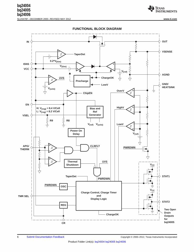
2• Highly Integrated Solution With FET PassThe bq2400x series ICs are advanced Li-Ion linearTransistor and Reverse-Blocking Schottky andcharge management devices for highly integrated andThermal Protectionspace-limited applications. They combine high-
• Integrated Voltage and Current Regulation accuracy current and voltage regulation; FET pass-With Programmable Charge Current transistor and reverse-blocking Schottky; battery
conditioning, temperature, or input-power monitoring;• High-Accuracy Voltage Regulation (±1%)charge termination; charge-status indication; and• Ideal for Low-Dropout Linear Charger Designscharge timer in a small package.for Two-Cell Li-Ion Packs With Coke or
Graphite Anodes The bq2400x measures battery temperature using anexternal thermistor. For safety, the bq2400x inhibits• Up to 1.2-A Continuous Charge Currentcharge until the battery temperature is within the
• Safety-Charge Timer During Preconditioning user-defined thresholds. Alternatively, the user canand Fast Charge monitor the input voltage to qualify charge. The
bq2400x series then charge the battery in three• Integrated Cell Conditioning for Revivingphases: preconditioning, constant current, andDeeply Discharged Cells and Minimizing Heatconstant voltage. If the battery voltage is below theDissipation During Initial Stage of Chargeinternal low-voltage threshold, the bq2400x uses low-• Optional Temperature or Input-Power current precharge to condition the battery. A
Monitoring Before and During Charge preconditioning timer provides additional safety.• Various Charge-Status Output Options for Following pre- conditioning, the bq2400x applies a
Driving Single, Double, or Bicolor LEDs or constant-charge current to the battery. An externalsense-resistor sets the magnitude of the current. TheHost-Processor Interfaceconstant-current phase is maintained until the battery• Charge Termination by Minimum Current andreaches the charge-regulation voltage. The bq2400xTime then transitions to the constant voltage phase. The
• Low-Power Sleep Mode user can configure the device for cells with eithercoke or graphite anodes. The accuracy of the voltage• Packaging: 20-Lead TSSOP PowerPAD™regulation is better than ±1% over the operatingjunction temperature and supply voltage range.APPLICATIONSCharge is terminated by maximum time or minimum• PDAstaper current detection• Internet AppliancesThe bq2400x automatically restarts the charge if the• MP3 Playersbattery voltage falls below an internal recharge
• Digital Cameras threshold.
1
Please be aware that an important notice concerning availability, standard warranty, and use in critical applications ofTexas Instruments semiconductor products and disclaimers thereto appears at the end of this data sheet.
2PowerPAD is a trademark of Texas Instruments.
PRODUCTION DATA information is current as of publication date. Copyright © 2000–2012, Texas Instruments IncorporatedProducts conform to specifications per the terms of the TexasInstruments standard warranty. Production processing does notnecessarily include testing of all parameters.
bq24004bq24005bq24006SLUS476F –DECEMBER 2000–REVISED MAY 2012 www.ti.com
These devices have limited built-in ESD protection. The leads should be shorted together or the device placed in conductive foamduring storage or handling to prevent electrostatic damage to the MOS gates.
ORDERING INFORMATIONPACKAGE
CHARGE STATUSTJ 20-LEAD HTTSOP PowerPAD™ CONFIGURATION(PWP) (1) (2)
bq24004PWP Single LED
–40°C to 125°C bq24005PWP 2 LEDs
bq24006PWP Single bicolor LED
(1) The PWP package is available taped and reeled. Add R suffix to device type (e.g., bq24005PWPR) to order. Quantities 2500 devicesper reel.
(2) For the most current package and ordering information, see the Package Option Addendum at the end of this document, or see the TIWeb site at www.ti.com.
PACKAGE DISSIPATION RATINGSTA ≤ 25°C DERATING FACTORPACKAGE ΘJA ΘJC POWER RATING ABOVE TA = 25°C
PWP (1) 30.88°C/W 1.19°C/W 3.238 W 0.0324 W/°C
(1) This data is based on using the JEDEC high-K board and topside traces, top and bottom thermal pad (6,5 × 3,4 mm), internal 1-oz.power and ground planes, 8 thermal via underneath the die connecting to ground plane.
ABSOLUTE MAXIMUM RATINGSover operating free-air temperature range unless otherwise noted (1)
bq24004bq24005bq24006
Supply voltage (VCC with respect to GND) 13.5 V
Input voltage (IN, ISNS, EN, APG/THERM/CR/STAT1/STAT2, VSENSE, TMR SEL, VSEL) (all with 13.5 Vrespect to GND)
Output current (OUT pins) 2 A
Output sink/source current (STAT1 and STAT2) 10 mA
TA Operating free-air temperature range –40°C to 70°C
Tstg Storage temperature range –65°C to 150°C
TJ Junction temperature range –40°C to 125°C
Lead temperature (Soldering, 10 s) 300°C
(1) Stresses beyond those listed under absolute maximum ratings may cause permanent damage to the device. These are stress ratingsonly, and functional operation of the device at these or any other conditions beyond those indicated under recommended operatingconditions is not implied. Exposure to absolute-maximum-rated conditions for extended periods may affect device reliability.
RECOMMENDED OPERATING CONDITIONSMIN MAX UNIT
VCC Supply voltage 8.4 10 V
VIN Input voltage 8.4 10 V
Continuous output current 1.2 A
TJ Operating junction temperature range –40 125 °C
2 Submit Documentation Feedback Copyright © 2000–2012, Texas Instruments Incorporated
Product Folder Link(s): bq24004 bq24005 bq24006
bq24004bq24005bq24006
www.ti.com SLUS476F –DECEMBER 2000–REVISED MAY 2012
ELECTRICAL CHARACTERISTICSover recommended operating junction temperature supply and input voltages, and VI (VCC) ≥ VI (IN) ( unless otherwise noted)
PARAMETER TEST CONDITIONS MIN TYP MAX UNIT
VCC current VCC > VCC_UVLO, EN ≤ V(IHEN) 1 mA
VCC current, standby mode EN ≤ V(ILEN) 1 µA
IN current, standby mode EN ≤ V(ILEN) 10 µA
VCC < VCC_UVLO, VO(OUT) = 8.6 V, VSENSE = 8.6 V 2 8Standby current (sum of currents µAinto OUT and VSENSE pins) EN ≤ V(ILEN), VO(OUT) = 8.6 V, VSENSE = 8.6 V 2 8
VOLTAGE REGULATION, 0°C ≤ TJ ≤ 125°C
VSEL = VSS, 0 < IO ≤ 1.2 A 8.118 8.20 8.282Output voltage V
VSEL = VCC, 0 < IO ≤ 1.2 A 8.316 8.40 8.484
Load regulation 1 mA ≤ IO≤ 1.2 A,VCC = 10 V, VI(IN)= 5 V,TJ = 25°C 1 mV
Line regulation VO(OUT) + VDO + V(ilim)MAX < VI(VCC) < 10 V, TJ = 25°C 0.01 %/V
Dropout voltage = VI(IN)-Vout IO = 1.2 A, VO(OUT) + V(DO) + V(ilim)MAX < VI(VCC) < 10 V 0.5 V
CURRENT REGULATION, 0°C ≤ TJ ≤ 125°C
Current regulation threshold, VSENSE < VO(VSEL-LOW/HIGH) 0.093 0.1 0.107 VVI(limit)
VSENSE pulsed above V(LOWV) to IO = 10% of regulatedDelay time 1 msvalue (1)
IO increasing from 10% to 90% of regulated value,Rise time 0.1 1 msR(SNS) ≥ 0.2 Ω (1)
CURRENT SENSE RESISTOR, 0°C ≤ TJ ≤ 125°C
External current sense resistor 100 mA ≤ (ilim) ≤ 1.2 0.083 1 Ωrange R(SNS) A
PRECHARGE CURRENT REGULATION, 0°C ≤ TJ ≤ 125°C
Precharge current regulation VSENSE<V(LOWV), 0.083 ≤ R(SNS)≤ 1.0 Ω 40 60 80 mA
VCC UVLO COMPARATOR, 0°C ≤ TJ ≤ 125°C
Start threshold 8.75 8.9 9.0 V
Stop threshold 8.50 8.66 8.8 V
Hysteresis 50 mV
APG/THERM COMPARATOR, 0°C ≤ TJ ≤ 125°C
Upper trip threshold 1.480 1.498 1.515 V
Lower trip threshold 0.545 0.558 0.570 V
Input bias current 1 µA
LOWV COMPARATOR, 0°C ≤ TJ ≤ 125°C
Start threshold 5.60 5.75 5.90 V
Stop threshold 6.10 6.25 6.40 V
Hysteresis 100 mV
HIGHV (RECHARGE) COMPARATOR, 0°C ≤ TJ ≤ 125°C
Start threshold 7.70 7.85 8.00 V
OVERV COMPARATOR, 0°C ≤ TJ ≤ 125°C
Start threshold 8.85 9.00 9.15 V
Stop threshold 8.45 8.60 8.75 V
Hysteresis 50 mV
TAPERDET COMPARATOR, 0°C ≤ TJ ≤ 125°C
Trip threshold 12 18.5 25 mV
EN LOGIC INPUT, 0°C ≤ TJ ≤ 125°C
High-level input voltage 2.25 V
Low-level input voltage 0.8 V
Input pulldown resistance 100 200 kΩ
(1) Specified by design, not production tested.
Copyright © 2000–2012, Texas Instruments Incorporated Submit Documentation Feedback 3
Product Folder Link(s): bq24004 bq24005 bq24006

bq24004bq24005bq24006SLUS476F –DECEMBER 2000–REVISED MAY 2012 www.ti.com
ELECTRICAL CHARACTERISTICS (continued)over recommended operating junction temperature supply and input voltages, and VI (VCC) ≥ VI (IN) ( unless otherwise noted)
PARAMETER TEST CONDITIONS MIN TYP MAX UNIT
VSEL LOGIC INPUT, 0°C ≤ TJ ≤ 125°C
High-level input voltage 2.25 V
Low-level input voltage 0.8 V
Input pulldown resistance 100 200 kΩTMR SEL INPUT 0°C ≤ TJ ≤ 125°C
High-level input voltage 2.7 V
Low-level input voltage 0.6 V
Input bias current VI(TMR SEL) ≤ 5 V 15 µA
STAT1, STAT2 (bq24004, bq24006), 0°C ≤ TJ ≤ 125°C
IO = 10 mA 1.5Output (low) saturation voltage V
IO = 4 mA 0.6
IO = –10 mA VCC–1.5Output (high) saturation voltage V
IO = –4 mA VCC–0.5
Output turn on/off time IO = ± 10 mA, C = 100 pF (2) 100 µs
POWER-ON RESET (POR), 0°C ≤ TJ ≤ 125°C
POR delay See (2) 1.2 3 ms
POR falling-edge deglitch See (2) 25 75 µs
APG/THERM DELAY, 0°C ≤ TJ ≤ 125°C
APG/THERM falling-edge See (2) 25 75 µsdeglitch
TIMERS, 0°C ≤ TJ ≤ 125°C
TA = 25°C 15% 15%User-selectable timer accuracy
20% 20%
Precharge and taper timer 22.5 minute
THERMAL SHUTDOWN, 0°C ≤ TJ ≤ 125°C
Thermal trip See (2) 165 °C
Thermal hysteresis See (2) 10 °C
CR PIN, 0°C ≤ TJ ≤ 125°C
Output voltage 0 < IO(CR) < 100 µA 2.816 2.85 2.88 V
(2) Specified by design, not production tested.
4 Submit Documentation Feedback Copyright © 2000–2012, Texas Instruments Incorporated
Product Folder Link(s): bq24004 bq24005 bq24006

123
4 56789
10
201918
171615141312
11
N/CININ
VCCISNS
N/CAPG/THERM
ENVSEL
GND/HEATSINK
N/COUTOUTVSENSEAGNDN/CSTAT1TMR SELCRN/C
bq24004PWP PACKAGE
(TOP VIEW)
123
4 56789
10
201918
171615141312
11
N/CININ
VCCISNS
N/CAPG/THERM
ENVSEL
GND/HEATSINK
N/COUTOUTVSENSEAGNDSTAT2STAT1TMR SELCRN/C
bq24005, bq24006PWP PACKAGE
(TOP VIEW)
N/C - Do not connect
bq24004bq24005bq24006
www.ti.com SLUS476F –DECEMBER 2000–REVISED MAY 2012
PIN ASSIGNMENTS
TERMINAL FUNCTIONSTERMINAL
I/O DESCRIPTIONNAME NO.
AGND 16 Ground pin; connect close to the negative battery terminal.
APG/THERM 7 I Adapter power good input/thermistor sense input
CR 12 I Internal regulator bypass capacitor
EN 8 I Charge-enable input. Active-high enable input with internal pull down. Low-current stand-by modeactive when EN is low.
GND/HEATSIN 10 Ground pin; connect to PowerPAD heat-sink layout pattern.K
IN 2, 3 I Input voltage. This input provides the charging voltage for the battery.
ISNS 5 I Current sense input
N/C 1, 6, 11, No connect. These pins must be left floating. Pin 15 is N/C on bq24004PWP only.15, 20
OUT 18, 19 O Charge current output
STAT1 14 O Status display output 1
STAT2 15 O Status display output 2 (for bq24005 and bq24006 only)
TMR SEL 13 I Charge timer selection input
VCC 4 I Supply voltage
VSEL 9 I 8.2-V or 8.4-V charge regulation selection input
VSENSE 17 I Battery voltage sense input
Copyright © 2000–2012, Texas Instruments Incorporated Submit Documentation Feedback 5
Product Folder Link(s): bq24004 bq24005 bq24006
-
+
Charge Control, Charge Timerand
Display Logic
OSCVCC
VCC
STAT1
STAT2
TaperDet
REG
PWRDWN
CR
ChargeOK
PWRDWN
UVSThermalShutdown
TMR SEL
-
+
-
+
Power OnDelay
CLRFLTAPG/THERM
R9
Precharge
Bias andRef
Generator
V(ref) V(uvlo)
H: V(reg) = 8.4 V/CellL: V(reg) = 8.2 V/Cell
VSEL
EN
R8
ChipEN
UVS
V(uvlo)
+
-
ChargeOK
LowV
+
-
V(ilim)VCC
ISNS
-
+TaperDet
IN
V(ref)AGND
VSENSE
OUT
GND/HEATSINK
+
-
OverV
+
-
HighV
-
+LowV
V(ref)
PWRDWN
Two OpenDrainOutputsforbq24005
0.2*V(ilim)
bq24004bq24005bq24006SLUS476F –DECEMBER 2000–REVISED MAY 2012 www.ti.com
FUNCTIONAL BLOCK DIAGRAM
6 Submit Documentation Feedback Copyright © 2000–2012, Texas Instruments Incorporated
Product Folder Link(s): bq24004 bq24005 bq24006
T = 25 C
I = 100 mAO
A
o
T = 25 C
I = 100 mAO
A
o
T - Junction Temperature - CJo
V = 10 V
T = 25 C(IN)
Ao
bq24004bq24005bq24006
www.ti.com SLUS476F –DECEMBER 2000–REVISED MAY 2012
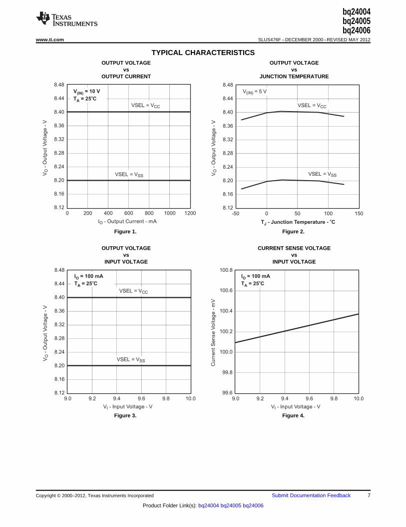
TYPICAL CHARACTERISTICSOUTPUT VOLTAGE OUTPUT VOLTAGE
vs vsOUTPUT CURRENT JUNCTION TEMPERATURE
Figure 1. Figure 2.
OUTPUT VOLTAGE CURRENT SENSE VOLTAGEvs vs
INPUT VOLTAGE INPUT VOLTAGE
Figure 3. Figure 4.
Copyright © 2000–2012, Texas Instruments Incorporated Submit Documentation Feedback 7
Product Folder Link(s): bq24004 bq24005 bq24006

T = 25 CA
o
T = 25 CA
o
V = 10 V
T = 25 C
CC
Ao
I = 100 mAO
T - Junction Temperature - CJo
T = 25 CA
o
bq24004bq24005bq24006SLUS476F –DECEMBER 2000–REVISED MAY 2012 www.ti.com
TYPICAL CHARACTERISTICS (continued)CURRENT SENSE VOLTAGE QUIESCENT CURRENT
vs vsJUNCTION TEMPERATURE INPUT VOLTAGE
Figure 5. Figure 6.
QUIESCENT CURRENT (POWER DOWN) DROPOUT VOLTAGEvs vs
INPUT VOLTAGE INPUT VOLTAGE
Figure 7. Figure 8.
8 Submit Documentation Feedback Copyright © 2000–2012, Texas Instruments Incorporated
Product Folder Link(s): bq24004 bq24005 bq24006

I-
Re
ve
rse
Cu
rre
nt
-A
Rm
T - Junction Temperature - CJo
T = 25 CAo
I-
Re
ve
rse
Cu
rre
nt
Le
ak
ag
e -
AR
m
T - Junction Temperature - CJo
V = 10 V
T = 25 C
CC
A
o
bq24004bq24005bq24006
www.ti.com SLUS476F –DECEMBER 2000–REVISED MAY 2012
TYPICAL CHARACTERISTICS (continued)DROPOUT VOLTAGE DROPOUT VOLTAGE
vs vsOUTPUT CURRENT JUNCTION TEMPERATURE
Figure 9. Figure 10.
REVERSE CURRENT REVERSE CURRENT LEAKAGEvs vs
JUNCTION TEMPERATURE VOLTAGE ON OUT PIN
Figure 11. Figure 12.
Copyright © 2000–2012, Texas Instruments Incorporated Submit Documentation Feedback 9
Product Folder Link(s): bq24004 bq24005 bq24006

U1
N/C N/C1 20
IN OUT2 19
IN OUT3 18
VCC VSENSE4 17
ISNS AGND5 16
N/C STAT26 15
APG/THM STAT17 14
VSEL CR9 12
EN TMR SEL8 13
GND N/C10 11
VCC
C20.1 µF
R10.1 Ω
C110 µF +
DC-
DC+
VCC
bq24005PWP
TEMP
PACK+
PACK-
R218.7 kΩ
C30.22 µF
+
-
C41 µF
BatteryPack
R4500 Ω
D1
VCC
R5500 Ω
D2
R395.3 kΩ
bq24004bq24005bq24006SLUS476F –DECEMBER 2000–REVISED MAY 2012 www.ti.com
APPLICATION INFORMATION
Figure 13. Li-ION/Li-POL Charger
• If the TMR SEL pin is left floating (3 HR time), a 10-pF capacitor should be installed between TMR SEL andCR.
• If a micro process is monitoring the STAT pins, it may be necessary to add some hysteresis into the feedbackto prevent the STAT pins from cycling while crossing the taper detect threshold (usually less than one halfsecond). See SLUU083 EVM or SLUU113 EVM for additional resistors used for the STAT pins.
FUNCTIONAL DESCRIPTION
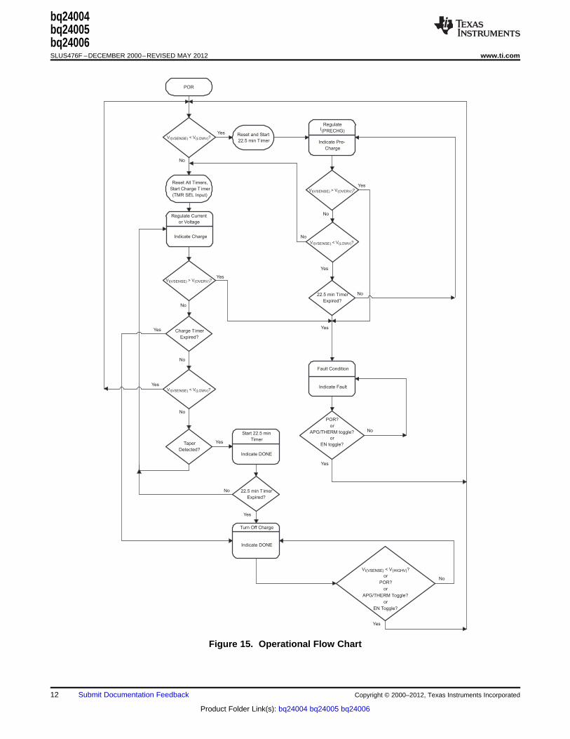
The bq2400x supports a precision current- and voltage-regulated Li-Ion charging system suitable for cells witheither coke or graphite anodes. See Figure 14 for a typical charge profile and Figure 15 for an operationalflowchart.
10 Submit Documentation Feedback Copyright © 2000–2012, Texas Instruments Incorporated
Product Folder Link(s): bq24004 bq24005 bq24006

PreconditioningPhase
Regulation VoltageV(OUT)
Current RegulationPhase
Voltage Regulation andCharge Termination Phase
Regulation CurrentI(lim)
Minimum ChargeVoltage V(LOWV)
PreconditioningCurrent I(PRECHG)
Charge Voltage
Charge Current
22.5 Minutes 22.5 Minutes
Charge Timer (3, 4.5 or 6 Hours)
Taper Detect
bq24004bq24005bq24006
www.ti.com SLUS476F –DECEMBER 2000–REVISED MAY 2012
Figure 14. Typical Charge Profile
Copyright © 2000–2012, Texas Instruments Incorporated Submit Documentation Feedback 11
Product Folder Link(s): bq24004 bq24005 bq24006
Yes
No
22.5 min Timer
Expired?
No
Yes
Indicate Fault
POR?
or
APG/THERM toggle?
or
EN toggle?
Yes
No
Yes
Charge Timer
Expired?
No
Indicate Pre-
Charge
RegulateI(PRECHG)
Indicate Charge
Regulate Current
or Voltage
Reset and Start
22.5 min Timer
POR
Reset All Timers,
Start Charge T imer
(TMR SEL Input)
No
Fault Condition
No
Yes
Indicate DONE
Turn Off Charge
Taper
Detected?
No
No
Yes
Yes
No
Yes
No
Yes
22.5 min Timer
Expired?
Yes
Yes
Indicate DONE
Start 22.5 min
Timer
VI(VSENSE) < V(HIGHV)?
or
POR?
or
APG/THERM Toggle?
or
EN Toggle?
VI(VSENSE) < V(LOWV)?
VI(VSENSE) > V(OVERV)?
VI(VSENSE) > V(OVERV)?
VI(VSENSE) < V(LOWV)?
VI(VSENSE) < V(LOWV)?
bq24004bq24005bq24006SLUS476F –DECEMBER 2000–REVISED MAY 2012 www.ti.com
Figure 15. Operational Flow Chart
12 Submit Documentation Feedback Copyright © 2000–2012, Texas Instruments Incorporated
Product Folder Link(s): bq24004 bq24005 bq24006

U1
N/C N/C1 20
IN OUT2 19
IN OUT3 18
VCC VSENSE4 17
ISNS AGND5 16
N/C STAT26 15
APG/THM STAT17 14
VSEL CR9 12
EN TMR SEL8 13
GND N/C10 11
bq24005PWP
TEMP
PACK+
PACK-
RT1
C30.22 µF
+
-
Battery Pack
RT2
NTC Thermistor
bq24004bq24005bq24006
www.ti.com SLUS476F –DECEMBER 2000–REVISED MAY 2012
Charge Qualification and Preconditioning The APG/THERM input can also be configured tomonitor either the adapter power or the batteryThe bq2400x starts a charge cycle when power istemperature using a thermistor. The bq2400xapplied while a battery is present. Chargesuspends charge if this input is outside the limits setqualification is based on battery voltage and theby the user. Refer to the APG/THERM input sectionAPG/THERM input.for additional details.
As shown in the block diagram, the internal LowVcomparator output prevents fast-charging a deeply APG/THERM Inputdepleted battery. When set, charging current is
The bq2400x continuously monitors temperature orprovided by a dedicated precharge current source.system input voltage by measuring the voltageThe precharge timer limits the precharge duration.between the APG/THERM (adapter powerThe precharge current also minimizes heatgood/thermistor) and GND. For temperature, adissipation in the pass element during the initial stagenegative- or a positive-temperature coefficientof charge.thermistor (NTC, PTC) and an external voltagedivider typically develop this voltage (see Figure 16).The bq2400x compares this voltage against itsinternal V(TP1) and V(TP2) thresholds to determine ifcharging is allowed. (See Figure 17.)
Figure 16. Temperature Sensing Circuit
Copyright © 2000–2012, Texas Instruments Incorporated Submit Documentation Feedback 13
Product Folder Link(s): bq24004 bq24005 bq24006

V(APG) VCCR2
(R1 R2)
where V(APG) is the voltage at the APG/THM pin.
bq24005PWP
RT1
VBVC 1
1RT2
1RC
RT2
VB RH RC 1VC
1VH
RH VBVH
1 RC VBVC
1
bq24004bq24005bq24006SLUS476F –DECEMBER 2000–REVISED MAY 2012 www.ti.com
If the charger designs incorporate a thermistor, theresistor divider RT1 and RT2 is calculated by usingthe following two equations.
First, calculate RT2.
then use the resistor value to find RT1.
Where:VB = VCR (bias voltage)RH = Resistance of the thermistor at the desiredhot trip thresholdRC = Resistance of the thermistor at the desired
Figure 18. APG Sensing Circuitcold trip thresholdVH = VP2 or the lower APG trip threshold
Values of resistors R1 and R2 can be calculatedVC = VP2 or the upper APG trip thresholdusing the following equation:
RT1 = Top resistor in the divider stringRT2 = Bottom resistor in the divider string
Current Regulation
The bq2400x provides current regulation while thebattery-pack voltage is less than the regulationvoltage. The current regulation loop effectivelyamplifies the error between a reference signal, Vilim,and the drop across the external sense resistor,RSNS.
Figure 17. Temperature Threshold
14 Submit Documentation Feedback Copyright © 2000–2012, Texas Instruments Incorporated
Product Folder Link(s): bq24004 bq24005 bq24006

R(SNS)V(ilim)I(REG)
where I(REG) is the desired charging current.
U1
N/C N/C1 20
IN OUT2 19
IN OUT3 18
VCC VSENSE4 17
ISNS AGND5 16
N/C STAT26 15
APG/THM STAT17 14
VSEL CR9 12
EN TMR SEL8 13
GND N/C10 11
VCC
C20.1 µF
R(SNS)
C110 µF +
DC-
DC+
VCC
bq24005PWP
bq24004bq24005bq24006
www.ti.com SLUS476F –DECEMBER 2000–REVISED MAY 2012
Figure 19. Current Sensing Circuit
Charge current feedback, applied through pin ISNS, phase of the charge and is reset at the beginning of amaintains regulation around a threshold of Vilim. The new charge cycle. Note that in the case of a faultfollowing formula calculates the value of the sense condition, such as an out-of-range signal on theresistor: APG/THERM input or a thermal shutdown, the
bq2400x suspends the timer.
TMRSEL STATE CHARGE TIME
Floating(1) 3 hours
Low 6 hours
High 4.5 hoursVoltage Monitoring and Regulation (1)To improve noise immunity, it is recommended that a minimum
of 10 pF capacitor be tied to Vss on a floating pin.Voltage regulation feedback is through pin VSENSE.This input is tied directly to the positive side of the
Minimum Current: The bq2400x monitors thebattery pack. The bq2400x supports cells with eithercharging current during the voltage regulation phase.coke (8.2 V) or graphite (8.4 V) anode. Pin VSELThe bq2400x initiates a 22-minute timer once theselects the charge regulation voltage.current falls below the taperdet trip threshold. Fastcharge is terminated once the 22-minute timerVSEL STATE CHARGE REGULATIONexpires.(see Note) VOLTAGE
Low 8.2 VCharge Status Display
High 8.4 V
The three available options allow the user toNOTE: VSEL should not be left floating.configure the charge status display for single LED(bq24004), two individual LEDs (bq24005) or aCharge Terminationbicolor LED (bq24006). The output stage is totem
The bq2400x continues with the charge cycle until pole for the bq24004 and bq24006 and open-drain fortermination by one of the two possible termination the bq24005. The following tables summarize theconditions: operation of the three options:
Maximum Charge Time: The bq2400x sets the Table 1. bq24004 (Single LED)maximum charge time through pin TMRSEL. The
CHARGE STATE STAT1TMR SEL pin allows the user to select between threedifferent total charge-time timers (3, 4, 5, or 6 hours). Precharge ON (LOW)The charge timer is initiated after the preconditioning Fast charge ON (LOW)
FAULT Flashing (1 Hz, 50% duty cycle)
Copyright © 2000–2012, Texas Instruments Incorporated Submit Documentation Feedback 15
Product Folder Link(s): bq24004 bq24005 bq24006
bq24004bq24005bq24006SLUS476F –DECEMBER 2000–REVISED MAY 2012 www.ti.com
Table 1. bq24004 (Single LED) (continued) Table 2. bq24005 (2 Individual LEDs) (continued)
CHARGE STATE STAT1 STAT2CHARGE STATE STAT1 (RED) (GREEN)Done (>90%) OFF (HIGH)Battery absent OFF OFF(1)
Sleep-mode OFF (HIGH)(1)If thermistor is used, then the Green LED is off.APG/Therm invalid OFF (HIGH)
Thermal shutdown OFF (HIGH)Table 3. bq24006 (Single Bicolor LED)
Battery absent OFF (HIGH)LED2 APPARENTCHARGE STATE LED1 (RED) (GREEN) COLOR
Table 2. bq24005 (2 Individual LEDs)Precharge ON (LOW) OFF (HIGH) RED
STAT2CHARGE STATE STAT1 (RED) Fast charge ON (LOW) OFF (HIGH) RED(GREEN)FAULT ON (LOW) ON (LOW) YELLOWPrecharge ON (LOW) OFFDone (>90%) OFF (HIGH) ON (LOW) GREENFast charge ON (LOW) OFFSleep-mode OFF (HIGH) OFF (HIGH) OFFFlashing (1 Hz,50% dutyFAULT OFFcycle) APG/Therminvalid OFF (HIGH) OFF (HIGH) OFF
Done (>90%) OFF ON (LOW) Thermal shutdown OFF (HIGH) OFF (HIGH) OFF
Sleep-mode OFF OFF Battery absent OFF (HIGH) OFF (HIGH)(1) OFF(1)
APG/Therm invalid OFF OFF (1)If thermistor is used, then the Green LED is off.
Thermal shutdown OFF OFF
Thermal Shutdown
The bq2400x monitors the junction temperature TJ of the DIE and suspends charging if TJ exceeds 165°C.Charging resumes when TJ falls below 155°C.
DETAILED DESCRIPTION
POWER FET VOLTAGE SENSE
The integrated transistor is a P-channel MOSFET. To achieve maximum voltage regulation accuracy,The power FET features a reverse-blocking Schottky the bq2400x uses the feedback on the VSENSE pin.diode, which prevents current flow from OUT to IN. Externally, this pin should be connected as close to
the battery cell terminals as possible. For additionalAn internal thermal-sense circuit shuts off the power safety, a 10-kΩ internal pullup resistor is connectedFET when the junction temperature rises to between the VSENSE and OUT pins.approximately 165°C. Hysteresis is built into thethermal sense circuit. After the device has cooled ENABLE (EN)approximately 10°C, the power FET turns back on.The power FET continues to cycle off and on until the The logic EN input is used to enable or disable thefault is removed. IC. A high-level signal on this pin enables the
bq2400x. A low-level signal disables the IC andCURRENT SENSE places the device in a low-power standby mode.
The bq2400x regulates current by sensing, on theISNS pin, the voltage drop developed across anexternal sense resistor. The sense resistor must beplaced between the supply voltage (Vcc) and theinput of the IC (IN pins).
16 Submit Documentation Feedback Copyright © 2000–2012, Texas Instruments Incorporated
Product Folder Link(s): bq24004 bq24005 bq24006

DIE
Side View (a)
End View (b)
Bottom View (c)
DIE
Thermal
Pad
bq24004bq24005bq24006
www.ti.com SLUS476F –DECEMBER 2000–REVISED MAY 2012
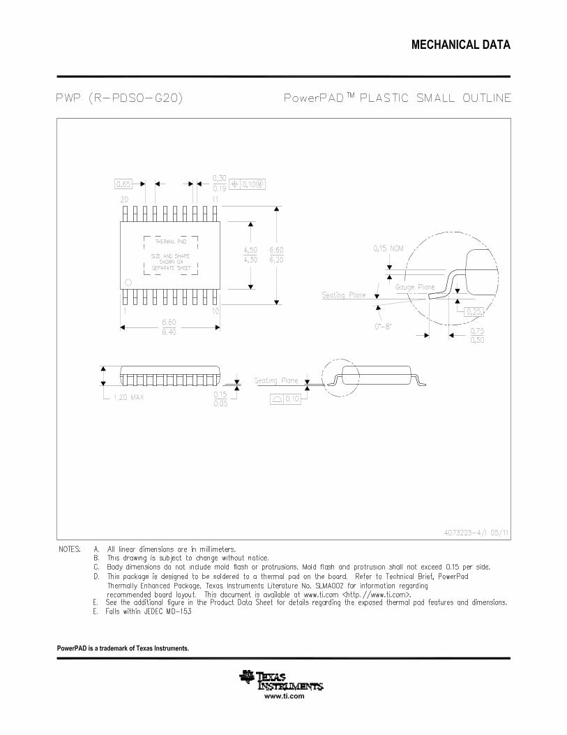
THERMAL INFORMATION
THERMALLY ENHANCED TSSOP-20
The thermally enhanced PWP package is based onthe 20-pin TSSOP, but includes a thermal pad(seeFigure 20) to provide an effective thermal contactbetween the IC and the PWB.
Traditionally, surface mount and power have beenmutually exclusive terms. A variety of scaled-downTO220-type packages have leads formed as gullwings to make them applicable for surface-mountapplications. These packages, however, suffer fromseveral shortcomings: they do not address the verylow profile requirements (<2 mm) of many of today'sadvanced systems, and they do not offer a pin-counthigh enough to accommodate increasing integration.On the other hand, traditional low-power surface-mount packages require power-dissipation deratingthat severely limits the usable range of many high-performance analog circuits.
The PWP package (thermally enhanced TSSOP)combines fine-pitch surface-mount technology withthermal performance comparable to much largerpower packages.
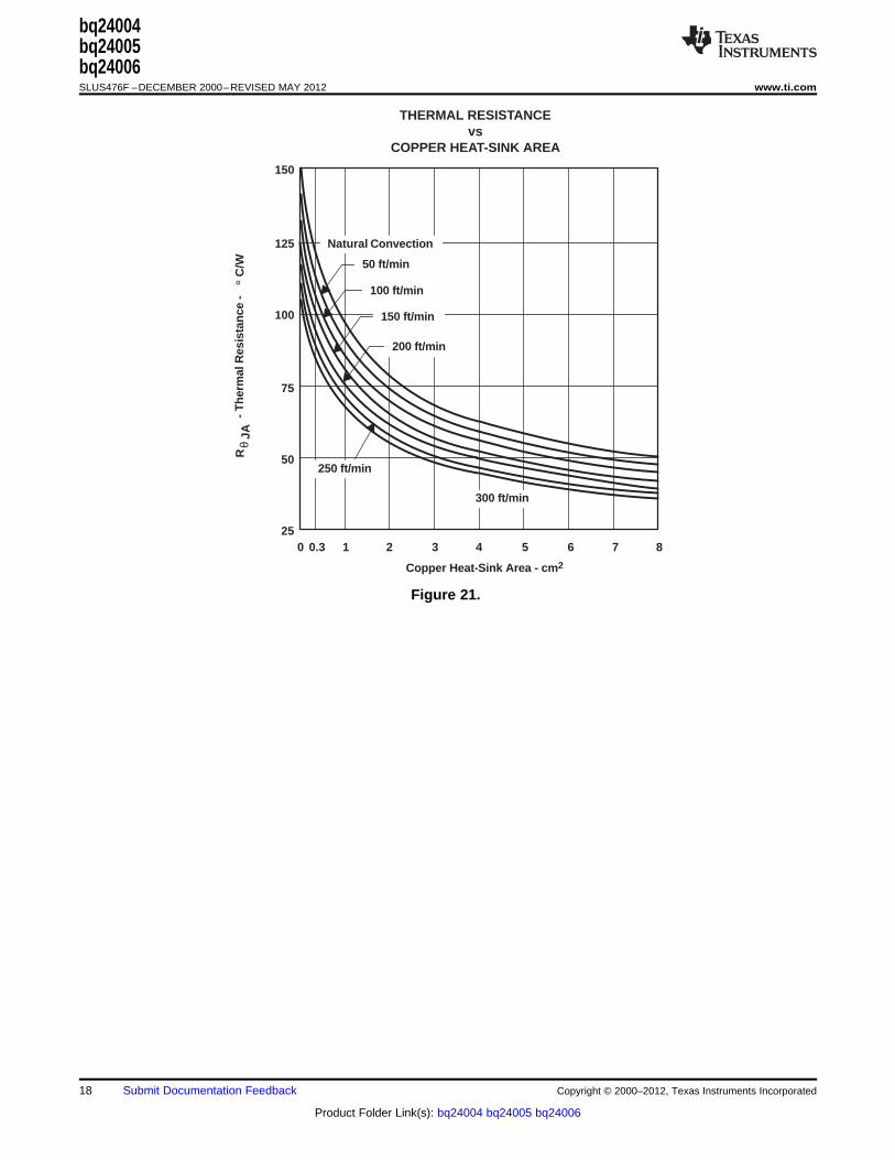
The PWP package is designed to optimize the heattransfer to the PWB. Because of the very small size Figure 20. Views of Thermally Enhancedand limited mass of a TSSOP package, thermal PWP Packageenhancement is achieved by improving the thermalconduction paths that remove heat from the Because the conduction path has been enhanced,component. The thermal pad is formed using a lead- power-dissipation capability is determined by theframe design (patent pending) and manufacturing thermal considerations in the PWB design. Fortechnique to provide the user with direct connection example, simply adding a localized copper planeto the heat-generating IC. When this pad is soldered (heat-sink surface), which is coupled to the thermalor otherwise coupled to an external heat dissipator, pad, enables the PWP package to dissipate 2.5 W inhigh power dissipation in the ultrathin, fine-pitch, free air. (Reference Figure 22(a),8 cm2 of coppersurface-mount package can be reliably achieved. heat sink and natural convection.) Increasing the
heat-sink size increases the power dissipation rangefor the component. The power dissipation limit can befurther improved by adding airflow to a PWB/ICassembly. (See Figure 22(b) and Figure 22(c).) Theline drawn at 0.3 cm2 in Figure 21 and Figure 22indicates performance at the minimum recommendedheat-sink size.
Copyright © 2000–2012, Texas Instruments Incorporated Submit Documentation Feedback 17
Product Folder Link(s): bq24004 bq24005 bq24006
100
75
50
250 2 3 5
- Th
erm
al R
esis
tan
ce -
125
THERMAL RESISTANCEvs
COPPER HEAT-SINK AREA
150
7 81 4 60.3
Natural Convection
50 ft/min
250 ft/min
300 ft/min
C/W
°
Copper Heat-Sink Area - cm2
100 ft/min
150 ft/min
200 ft/min
RJA
θ
bq24004bq24005bq24006SLUS476F –DECEMBER 2000–REVISED MAY 2012 www.ti.com
Figure 21.
18 Submit Documentation Feedback Copyright © 2000–2012, Texas Instruments Incorporated
Product Folder Link(s): bq24004 bq24005 bq24006

1
0.5
3
00 2 4 6
2
1.5
2.5
3.5
80.3
300 ft/min
150 ft/min
Natural Convection
Copper Heat-Sink Size - cm2
TA = 55°C
(b)
1
0.5
3
00 2 4 6
2
1.5
2.5
3.5
80.3
300 ft/min150 ft/min
Natural Convection
Copper Heat-Sink Size - cm2
TA = 105°C
(c)
1
0.5
3
00 2 4 6
- Po
wer
Dis
sip
atio
n L
imit
- W
2
1.5
2.5
3.5
80.3
300 ft/min
150 ft/min
Natural Convection
PD
Copper Heat-Sink Size - cm2
TA = 25°C
(a)
- Po
wer
Dis
sip
atio
n L
imit
- W
PD
- Po
wer
Dis
sip
atio
n L
imit
- W
PD
bq24004bq24005bq24006
www.ti.com SLUS476F –DECEMBER 2000–REVISED MAY 2012
Figure 22. Power Ratings of the PWP Package at Ambient Temperatures of 25°C, 55°C, and 105°C
Copyright © 2000–2012, Texas Instruments Incorporated Submit Documentation Feedback 19
Product Folder Link(s): bq24004 bq24005 bq24006
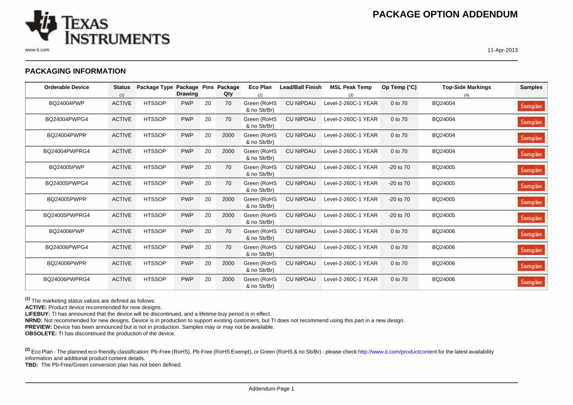
PACKAGE OPTION ADDENDUM
www.ti.com 11-Apr-2013
Addendum-Page 1
PACKAGING INFORMATION
Orderable Device Status(1)
Package Type PackageDrawing
Pins PackageQty
Eco Plan(2)
Lead/Ball Finish MSL Peak Temp(3)
Op Temp (°C) Top-Side Markings(4)
Samples
BQ24004PWP ACTIVE HTSSOP PWP 20 70 Green (RoHS& no Sb/Br)
CU NIPDAU Level-2-260C-1 YEAR 0 to 70 BQ24004
BQ24004PWPG4 ACTIVE HTSSOP PWP 20 70 Green (RoHS& no Sb/Br)
CU NIPDAU Level-2-260C-1 YEAR 0 to 70 BQ24004
BQ24004PWPR ACTIVE HTSSOP PWP 20 2000 Green (RoHS& no Sb/Br)
CU NIPDAU Level-2-260C-1 YEAR 0 to 70 BQ24004
BQ24004PWPRG4 ACTIVE HTSSOP PWP 20 2000 Green (RoHS& no Sb/Br)
CU NIPDAU Level-2-260C-1 YEAR 0 to 70 BQ24004
BQ24005PWP ACTIVE HTSSOP PWP 20 70 Green (RoHS& no Sb/Br)
CU NIPDAU Level-2-260C-1 YEAR -20 to 70 BQ24005
BQ24005PWPG4 ACTIVE HTSSOP PWP 20 70 Green (RoHS& no Sb/Br)
CU NIPDAU Level-2-260C-1 YEAR -20 to 70 BQ24005
BQ24005PWPR ACTIVE HTSSOP PWP 20 2000 Green (RoHS& no Sb/Br)
CU NIPDAU Level-2-260C-1 YEAR -20 to 70 BQ24005
BQ24005PWPRG4 ACTIVE HTSSOP PWP 20 2000 Green (RoHS& no Sb/Br)
CU NIPDAU Level-2-260C-1 YEAR -20 to 70 BQ24005
BQ24006PWP ACTIVE HTSSOP PWP 20 70 Green (RoHS& no Sb/Br)
CU NIPDAU Level-2-260C-1 YEAR 0 to 70 BQ24006
BQ24006PWPG4 ACTIVE HTSSOP PWP 20 70 Green (RoHS& no Sb/Br)
CU NIPDAU Level-2-260C-1 YEAR 0 to 70 BQ24006
BQ24006PWPR ACTIVE HTSSOP PWP 20 2000 Green (RoHS& no Sb/Br)
CU NIPDAU Level-2-260C-1 YEAR 0 to 70 BQ24006
BQ24006PWPRG4 ACTIVE HTSSOP PWP 20 2000 Green (RoHS& no Sb/Br)
CU NIPDAU Level-2-260C-1 YEAR 0 to 70 BQ24006
(1) The marketing status values are defined as follows:ACTIVE: Product device recommended for new designs.LIFEBUY: TI has announced that the device will be discontinued, and a lifetime-buy period is in effect.NRND: Not recommended for new designs. Device is in production to support existing customers, but TI does not recommend using this part in a new design.PREVIEW: Device has been announced but is not in production. Samples may or may not be available.OBSOLETE: TI has discontinued the production of the device.
(2) Eco Plan - The planned eco-friendly classification: Pb-Free (RoHS), Pb-Free (RoHS Exempt), or Green (RoHS & no Sb/Br) - please check http://www.ti.com/productcontent for the latest availabilityinformation and additional product content details.TBD: The Pb-Free/Green conversion plan has not been defined.

PACKAGE OPTION ADDENDUM
www.ti.com 11-Apr-2013
Addendum-Page 2
Pb-Free (RoHS): TI's terms "Lead-Free" or "Pb-Free" mean semiconductor products that are compatible with the current RoHS requirements for all 6 substances, including the requirement thatlead not exceed 0.1% by weight in homogeneous materials. Where designed to be soldered at high temperatures, TI Pb-Free products are suitable for use in specified lead-free processes.Pb-Free (RoHS Exempt): This component has a RoHS exemption for either 1) lead-based flip-chip solder bumps used between the die and package, or 2) lead-based die adhesive used betweenthe die and leadframe. The component is otherwise considered Pb-Free (RoHS compatible) as defined above.Green (RoHS & no Sb/Br): TI defines "Green" to mean Pb-Free (RoHS compatible), and free of Bromine (Br) and Antimony (Sb) based flame retardants (Br or Sb do not exceed 0.1% by weightin homogeneous material)
(3) MSL, Peak Temp. -- The Moisture Sensitivity Level rating according to the JEDEC industry standard classifications, and peak solder temperature.
(4) Multiple Top-Side Markings will be inside parentheses. Only one Top-Side Marking contained in parentheses and separated by a "~" will appear on a device. If a line is indented then it is acontinuation of the previous line and the two combined represent the entire Top-Side Marking for that device.
Important Information and Disclaimer:The information provided on this page represents TI's knowledge and belief as of the date that it is provided. TI bases its knowledge and belief on informationprovided by third parties, and makes no representation or warranty as to the accuracy of such information. Efforts are underway to better integrate information from third parties. TI has taken andcontinues to take reasonable steps to provide representative and accurate information but may not have conducted destructive testing or chemical analysis on incoming materials and chemicals.TI and TI suppliers consider certain information to be proprietary, and thus CAS numbers and other limited information may not be available for release.
In no event shall TI's liability arising out of such information exceed the total purchase price of the TI part(s) at issue in this document sold by TI to Customer on an annual basis.

TAPE AND REEL INFORMATION
*All dimensions are nominal
Device PackageType
PackageDrawing
Pins SPQ ReelDiameter
(mm)
ReelWidth
W1 (mm)
A0(mm)
B0(mm)
K0(mm)
P1(mm)
W(mm)
Pin1Quadrant
BQ24004PWPR HTSSOP PWP 20 2000 330.0 16.4 6.95 7.1 1.6 8.0 16.0 Q1
BQ24005PWPR HTSSOP PWP 20 2000 330.0 16.4 6.95 7.1 1.6 8.0 16.0 Q1
BQ24006PWPR HTSSOP PWP 20 2000 330.0 16.4 6.95 7.1 1.6 8.0 16.0 Q1
PACKAGE MATERIALS INFORMATION
www.ti.com 14-Jul-2012
Pack Materials-Page 1

*All dimensions are nominal
Device Package Type Package Drawing Pins SPQ Length (mm) Width (mm) Height (mm)
BQ24004PWPR HTSSOP PWP 20 2000 367.0 367.0 38.0
BQ24005PWPR HTSSOP PWP 20 2000 367.0 367.0 38.0
BQ24006PWPR HTSSOP PWP 20 2000 367.0 367.0 38.0
PACKAGE MATERIALS INFORMATION
www.ti.com 14-Jul-2012
Pack Materials-Page 2


IMPORTANT NOTICE
Texas Instruments Incorporated and its subsidiaries (TI) reserve the right to make corrections, enhancements, improvements and otherchanges to its semiconductor products and services per JESD46, latest issue, and to discontinue any product or service per JESD48, latestissue. Buyers should obtain the latest relevant information before placing orders and should verify that such information is current andcomplete. All semiconductor products (also referred to herein as “components”) are sold subject to TI’s terms and conditions of salesupplied at the time of order acknowledgment.TI warrants performance of its components to the specifications applicable at the time of sale, in accordance with the warranty in TI’s termsand conditions of sale of semiconductor products. Testing and other quality control techniques are used to the extent TI deems necessaryto support this warranty. Except where mandated by applicable law, testing of all parameters of each component is not necessarilyperformed.TI assumes no liability for applications assistance or the design of Buyers’ products. Buyers are responsible for their products andapplications using TI components. To minimize the risks associated with Buyers’ products and applications, Buyers should provideadequate design and operating safeguards.TI does not warrant or represent that any license, either express or implied, is granted under any patent right, copyright, mask work right, orother intellectual property right relating to any combination, machine, or process in which TI components or services are used. Informationpublished by TI regarding third-party products or services does not constitute a license to use such products or services or a warranty orendorsement thereof. Use of such information may require a license from a third party under the patents or other intellectual property of thethird party, or a license from TI under the patents or other intellectual property of TI.Reproduction of significant portions of TI information in TI data books or data sheets is permissible only if reproduction is without alterationand is accompanied by all associated warranties, conditions, limitations, and notices. TI is not responsible or liable for such altereddocumentation. Information of third parties may be subject to additional restrictions.Resale of TI components or services with statements different from or beyond the parameters stated by TI for that component or servicevoids all express and any implied warranties for the associated TI component or service and is an unfair and deceptive business practice.TI is not responsible or liable for any such statements.Buyer acknowledges and agrees that it is solely responsible for compliance with all legal, regulatory and safety-related requirementsconcerning its products, and any use of TI components in its applications, notwithstanding any applications-related information or supportthat may be provided by TI. Buyer represents and agrees that it has all the necessary expertise to create and implement safeguards whichanticipate dangerous consequences of failures, monitor failures and their consequences, lessen the likelihood of failures that might causeharm and take appropriate remedial actions. Buyer will fully indemnify TI and its representatives against any damages arising out of the useof any TI components in safety-critical applications.In some cases, TI components may be promoted specifically to facilitate safety-related applications. With such components, TI’s goal is tohelp enable customers to design and create their own end-product solutions that meet applicable functional safety standards andrequirements. Nonetheless, such components are subject to these terms.No TI components are authorized for use in FDA Class III (or similar life-critical medical equipment) unless authorized officers of the partieshave executed a special agreement specifically governing such use.Only those TI components which TI has specifically designated as military grade or “enhanced plastic” are designed and intended for use inmilitary/aerospace applications or environments. Buyer acknowledges and agrees that any military or aerospace use of TI componentswhich have not been so designated is solely at the Buyer's risk, and that Buyer is solely responsible for compliance with all legal andregulatory requirements in connection with such use.TI has specifically designated certain components as meeting ISO/TS16949 requirements, mainly for automotive use. In any case of use ofnon-designated products, TI will not be responsible for any failure to meet ISO/TS16949.
Products ApplicationsAudio www.ti.com/audio Automotive and Transportation www.ti.com/automotiveAmplifiers amplifier.ti.com Communications and Telecom www.ti.com/communicationsData Converters dataconverter.ti.com Computers and Peripherals www.ti.com/computersDLP® Products www.dlp.com Consumer Electronics www.ti.com/consumer-appsDSP dsp.ti.com Energy and Lighting www.ti.com/energyClocks and Timers www.ti.com/clocks Industrial www.ti.com/industrialInterface interface.ti.com Medical www.ti.com/medicalLogic logic.ti.com Security www.ti.com/securityPower Mgmt power.ti.com Space, Avionics and Defense www.ti.com/space-avionics-defenseMicrocontrollers microcontroller.ti.com Video and Imaging www.ti.com/videoRFID www.ti-rfid.comOMAP Applications Processors www.ti.com/omap TI E2E Community e2e.ti.comWireless Connectivity www.ti.com/wirelessconnectivity
Mailing Address: Texas Instruments, Post Office Box 655303, Dallas, Texas 75265Copyright © 2016, Texas Instruments Incorporated