small diameter tio2 nanotubes with enhanced photoresponsivity
TRANSCRIPT
Electrochemistry Communications 28 (2013) 107–110
Contents lists available at SciVerse ScienceDirect
Electrochemistry Communications
j ourna l homepage: www.e lsev ie r .com/ locate /e lecom
Small diameter TiO2 nanotubes with enhanced photoresponsivity
Guohua Liu, Nils Hoivik, Kaiying Wang ⁎Department of Micro and Nano Systems Technology, Vestfold University College, Horten, 3184, Norway
⁎ Corresponding author. Tel.: +47 3303 7721; fax: +E-mail address: [email protected] (K. Wang).
1388-2481/$ – see front matter © 2012 Elsevier B.V. Allhttp://dx.doi.org/10.1016/j.elecom.2012.12.020
a b s t r a c t
a r t i c l e i n f oArticle history:Received 19 October 2012Received in revised form 16 December 2012Accepted 19 December 2012Available online 29 December 2012
Keywords:TiO2 nanotubeDiameterInternal gainPhotoresponsivity
We report ultraviolet (UV) light detection of thin wall TiO2 nanotubes (TNTs) with open diameter ~20 nmobtained by a two anodization procedure. This small diameter nanotubular geometry shows significant en-hancement of the photoresponsivity and results in a large increase of photocurrent. The photocurrent isone order higher than that of classical nanotubes with diameter of 140 nm at −1.0 V bias. We attributethis improvement to the modulation of hole carrier density as a result of field effects from thediameter-dependent population of the surface-trapped electrons. This finding demonstrates inherent size ef-fects of internal gain in semiconductor nanotubes.
© 2012 Elsevier B.V. All rights reserved.
1. Introduction
Nanostructured materials are attractive for photon detectionbecause of their large active surface area and potential integrationwith conventional electronics [1,2]. TiO2 nanostructures such asnanotubes, nanowires/rods are one of the main groups for the funda-mental research and development of real-world nanoelectronics[3–6]. The distinctive UV absorption ability makes TiO2 suitable forUV detection against the background of infrared and visible light[5]. The anisotropic geometry of the one-dimensional (1D) structurefacilitates rapid transport of carrier, which is crucial for optimizingthe carrier collection efficiency [5,6].
Various aspects of TiO2 photodetectors have been addressed bydownsizing from bulk to nanometer in the literature. Earlier studiesare devoted to understand the dynamics of the transport, trappingand recombination of charge carriers generated in TiO2 nanoparticlefilms [7,8]. However, it is a challenge to extract the intrinsic transportproperties from the size effects in dense nanoparticle films. Subse-quent in situ observations of photoconduction properties over the1D TiO2 nanostructures provide a means of exploring the surfaceand size effects on the electrical transport phenomena [5,9–11].Nevertheless, their manufacturing is complicated and not suitablefor large-scale applications. Recent studies are focused on device per-formances by using TiO2 rods/tubes as building block that leads to afilling/decoration of nanostructures [6,12–16]. For such composites,it is difficult to extract details on rod/tube-induced transport proper-ties as that represents a mixture of material behavior. Despite theprogress, fundamental questions about the internal electronic
47 3303 1103.
rights reserved.
structure, the effect of the large surface or small size in comparisonto its bulk, and size dependent transport phenomena in 1D TiO2
nanomaterials remain scarcely answered up to now.In this paper, we propose a facile procedure to synthesize crystal-
line, small diameter ~20 nm TiO2 nanotubes (TNTs) on Ti foils for un-derstanding size dependent transport in 1D TiO2 nanomaterials. Weuse such small diameter TNTs in UV detection and compare theirbehavior with the performance of the nanotube diameter~140 nm.The highlights of this work are (i) photoconductive study of smalldiameter TNTs with thin wall prepared by a two anodization step,(ii) demonstrating inherent size effects of internal gain in semicon-ductor nanotubes.
2. Experimental details
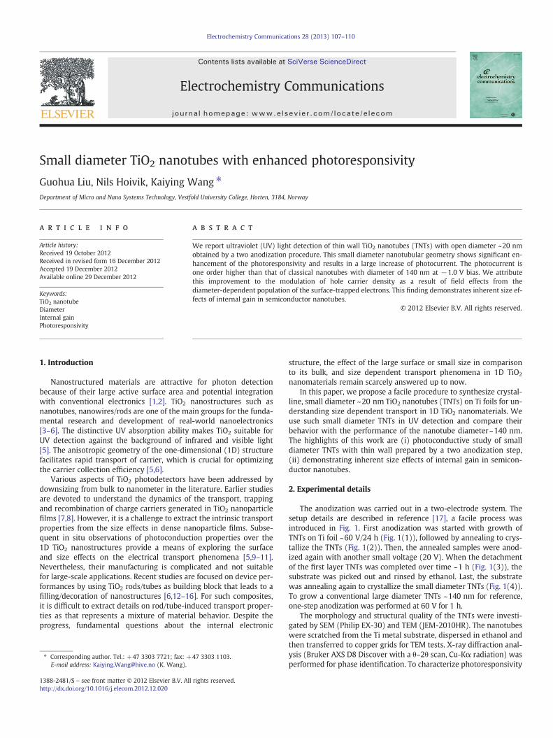
The anodization was carried out in a two-electrode system. Thesetup details are described in reference [17], a facile process wasintroduced in Fig. 1. First anodization was started with growth ofTNTs on Ti foil ~60 V/24 h (Fig. 1(1)), followed by annealing to crys-tallize the TNTs (Fig. 1(2)). Then, the annealed samples were anod-ized again with another small voltage (20 V). When the detachmentof the first layer TNTs was completed over time ~1 h (Fig. 1(3)), thesubstrate was picked out and rinsed by ethanol. Last, the substratewas annealing again to crystallize the small diameter TNTs (Fig. 1(4)).To grow a conventional large diameter TNTs ~140 nm for reference,one-step anodization was performed at 60 V for 1 h.
The morphology and structural quality of the TNTs were investi-gated by SEM (Philip EX-30) and TEM (JEM-2010HR). The nanotubeswere scratched from the Ti metal substrate, dispersed in ethanol andthen transferred to copper grids for TEM tests. X-ray diffraction anal-ysis (Bruker AXS D8 Discover with a θ–2θ scan, Cu-Kα radiation) wasperformed for phase identification. To characterize photoresponsivity
108 G. Liu et al. / Electrochemistry Communications 28 (2013) 107–110
of the crystallized TNTs, FTO glass was integrated on the surface ofTNT films to form photoconductive devices. Current–voltage (I–V)curves and time responses of the devices to light irradiation wererecorded with a Keithley 6430 source meter. A UV lamp (Tiede-50 W,λ=320 nm switchable) with tunable light intensity was selected aslight source. The light intensity was measured with an OAI-306power meter.
3. Results and discussion
Fig. 1A shows a top-view SEM image of the large diameter TNTsgrown at 60 V for 1 h. It is evident that the ordered nanotube arrayconsists of well-aligned nanotubes with an average inner diameterof 140 nm and wall thickness ~15 nm. The image of small diameterTNTs fabricated by the two anodization step, as shown Fig. 1B, indi-cates that the TNTs remain compact and no destructive changesafter detaching the first crystalline layer. The constituted TNTs areof an average diameter of 20 nm with a thin wall ~5 nm. Duringsecond anodic step, the first crystalline TNT layer serves as a bufferfor reducing the strength of electrical field and to protect the newformed nanotubes from chemical dissolution. Thus, uniform andsmall diameter nanotubes are realized after the second anodizationat 20 V for 1 h [18]. Minor amount of bottom parts of the first tubelayer left on the small diameter tubes, which serves as the electrontransporter for effective charge separation and rapid transport ofthe photogenerated electrons [19].
As the annealing temperature increases from room temperature to800 °C, the phase of as-prepared TNTs is changed as amorphous→anatase→rutile. The TNT morphology is collapsed at temperatureabove 600 °C. To form anatase TNT with preferred morphology andhigher photoelectric activity, annealing at 350–500 °C for 2–3 h inoxygen ambient is a reasonable temperature process [14,17,20]. The
(1) 1st anodization
(2) Annealing
(3) 2nd anodization
(4) Annealing
Detachment
(a)
Large diameter TNTs
(b)
Small diameter TNTs
Ti
Ti
Anatase TNTs
Small anatase TNTs
Ti
Fig. 1. The fabrication procedure (A) large dia
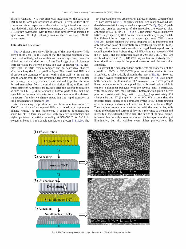
TEM image and selected-area electron diffraction (SAED) pattern of theTNTs are shown in Fig. 2. The high resolution TEM image shows a disor-dered characteristic for as-prepared amorphous TNTs (Fig. 2(a)). Crystal-lized and ordered structures of the nanotubes are observed afterannealing at 500 °C for 3 h (Fig. 2(b)). The image reveals distinctivelattice fringes spaced by 0.23 nm and exhibits anatase-type polycrystal-line Debye–Scherrer rings in the upper-right inset. XRD pattern(Fig. 2(c)) further confirms that the as-prepared TNT is amorphous andonly diffraction peaks of Ti substrate are detected (JCPDS file 44–1294).The crystallized counterpart shows three strong diffraction peaks corre-sponding to the three isolated rings. All diffractions are indexed (JCPDSfile 84–1286), and the diffraction peaks at 2θ=25.5°, 38.1°, 48.3° areidentified to be the (101), (004), (200) crystal faces respectively. Thereis no significant change in the pore diameter or wall thickness afterannealing.
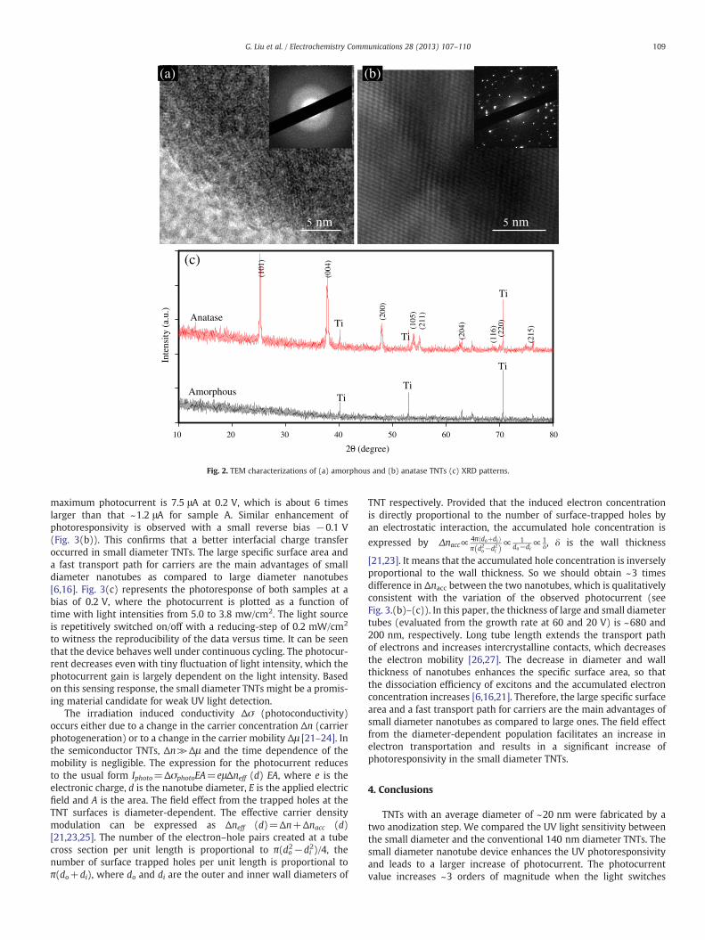
To extract the size-dependent photoelectrical properties of thecrystallized TNTs, a FTO/TNT/Ti photoconductive device is thenassembled, as schematically shown in the inset of Fig. 3(a). Two setsof linear sweep voltammograms are recorded in Fig. 3(a) underboth dark and UV illumination of 5 mW/cm2. I–V curves presentlinear dependence with the applied bias at forward region while itexhibits a nonlinear behavior with the reverse bias. In particular,with the reverse bias, the FTO/TNT/Ti heterojunction gives a betterphotoresponsivity with large ratios (Iphoto/Idark) approximately 735(Sample B) and 27 (Sample A) at −1.0 V. We assume that thephotoresponse is likely to be dominated by the Ti/TiO2 heterojunctionarea. Both samples show small dark current on the order of ~10 μA.The sample A keeps a larger dark current with the reverse bias, indi-cating the background current of devices is relevance to the sign andintensity of the external electric field. The device of the small diame-ter nanotubes not only shows pronounced photoresponse under lightillumination, but also exhibits even higher photocurrent. The
meter and (B) small diameter nanotubes.
20 (degree)
10 20 30 40 50 60 70 80
Inte
nsity
(a.
u.)
(101
)
(204
)
(211
)(1
05)
(200
)
(004
)
(215
)
(220
)(1
16)
Ti
Anatase
Amorphous Ti
Ti
TiTi
Ti
(c)
(a) (b)
5 nm 5 nm
Fig. 2. TEM characterizations of (a) amorphous and (b) anatase TNTs (c) XRD patterns.
109G. Liu et al. / Electrochemistry Communications 28 (2013) 107–110
maximum photocurrent is 7.5 μA at 0.2 V, which is about 6 timeslarger than that ~1.2 μA for sample A. Similar enhancement ofphotoresponsivity is observed with a small reverse bias −0.1 V(Fig. 3(b)). This confirms that a better interfacial charge transferoccurred in small diameter TNTs. The large specific surface area anda fast transport path for carriers are the main advantages of smalldiameter nanotubes as compared to large diameter nanotubes[6,16]. Fig. 3(c) represents the photoresponse of both samples at abias of 0.2 V, where the photocurrent is plotted as a function oftime with light intensities from 5.0 to 3.8 mw/cm2. The light sourceis repetitively switched on/off with a reducing-step of 0.2 mW/cm2
to witness the reproducibility of the data versus time. It can be seenthat the device behaves well under continuous cycling. The photocur-rent decreases even with tiny fluctuation of light intensity, which thephotocurrent gain is largely dependent on the light intensity. Basedon this sensing response, the small diameter TNTs might be a promis-ing material candidate for weak UV light detection.
The irradiation induced conductivity Δσ (photoconductivity)occurs either due to a change in the carrier concentration Δn (carrierphotogeneration) or to a change in the carrier mobility Δμ [21–24]. Inthe semiconductor TNTs, Δn≫Δμ and the time dependence of themobility is negligible. The expression for the photocurrent reducesto the usual form Iphoto=ΔσphotoEA=eμΔneff (d) EA, where e is theelectronic charge, d is the nanotube diameter, E is the applied electricfield and A is the area. The field effect from the trapped holes at theTNT surfaces is diameter-dependent. The effective carrier densitymodulation can be expressed as Δneff (d)=Δn+Δnacc (d)[21,23,25]. The number of the electron–hole pairs created at a tubecross section per unit length is proportional to π(do2−di
2)/4, thenumber of surface trapped holes per unit length is proportional toπ(do+di), where do and di are the outer and inner wall diameters of
TNT respectively. Provided that the induced electron concentrationis directly proportional to the number of surface-trapped holes byan electrostatic interaction, the accumulated hole concentration is
expressed by Δnacc∝ 4π doþdið Þπ d2o−d2ið Þ∝
1do−di
∝ 1δ, δ is the wall thickness
[21,23]. It means that the accumulated hole concentration is inverselyproportional to the wall thickness. So we should obtain ~3 timesdifference in Δnacc between the two nanotubes, which is qualitativelyconsistent with the variation of the observed photocurrent (seeFig. 3.(b)–(c)). In this paper, the thickness of large and small diametertubes (evaluated from the growth rate at 60 and 20 V) is ~680 and200 nm, respectively. Long tube length extends the transport pathof electrons and increases intercrystalline contacts, which decreasesthe electron mobility [26,27]. The decrease in diameter and wallthickness of nanotubes enhances the specific surface area, so thatthe dissociation efficiency of excitons and the accumulated electronconcentration increases [6,16,21]. Therefore, the large specific surfacearea and a fast transport path for carriers are the main advantages ofsmall diameter nanotubes as compared to large ones. The field effectfrom the diameter-dependent population facilitates an increase inelectron transportation and results in a significant increase ofphotoresponsivity in the small diameter TNTs.
4. Conclusions
TNTs with an average diameter of ~20 nm were fabricated by atwo anodization step. We compared the UV light sensitivity betweenthe small diameter and the conventional 140 nm diameter TNTs. Thesmall diameter nanotube device enhances the UV photoresponsivityand leads to a larger increase of photocurrent. The photocurrentvalue increases ~3 orders of magnitude when the light switches

t (s)0 50 100 150 200 250 300 350
I (µ
A)
-9
-6
-3
0
3
6
9
Voltage (V)-1.0 -0.5 0.0 0.5 1.0
I (µ
A)
-250
-225
-200
-175
-150
-125
-100
-75
-50
-25
0
25
BA
0.2 V
-0.1 V
(a)
(b)
t (s) 200 400 600 800 1000 1200
I (µ
A)
0
1
2
3
4
5
6
7(c)
Dark
Light on
Fig. 3. (a) I–V curves in dark and illumination, (b) photoresponses with differentbiases, and (c) time-dependent photoresponses.
110 G. Liu et al. / Electrochemistry Communications 28 (2013) 107–110
from off to on status. These observations are associated with themodulation of hole carrier density, which comes from field effects ofthe diameter-dependent population of the electrons. The understand-ing of this surface-induced size effect on electron transport is benefi-cial to the future design of optoelectronic devices.
References
[1] G. Konstantatos, E.H. Sargent, Nature Nanotechnology 5 (2010) 391–400.[2] L. Cao, J.S. White, J. Park, J.A. Schuller, B.M. Clemens, M.L. Brongersma, Nature Ma-
terials 8 (2009) 643–647.[3] O.K. Varghese, M. Paulose, C.A. Grimes, Nature Nanotechnology 4 (2009) 592–597.[4] G. Liu, K. Wang, N. Hoivik, H. Jakobsen, Solar Energy Materials and Solar Cells 98
(2012) 24–38.[5] R.S. Chen, C.A. Chen, H.Y. Tsai, W.C. Wang, Y.S. Huang, Journal of Physical Chem-
istry C 116 (2012) 4267–4272.[6] M. Ouyang, R. Bai, L. Yang, Q. Chen, Y. Han, M. Wang, Y. Yang, H. Chen, Journal of
Physical Chemistry C 112 (2008) 2343–2348.[7] H. Xue, X. Kong, Z. Liu, C. Liu, J. Zhou, W. Chen, Applied Physics Letters 90 (2007)
201118.[8] X. Kong, C. Liu, W. Dong, X. Zhang, C. Tao, L. Shen, J. Zhou, Y. Fei, S. Ruan, Applied
Physics Letters 94 (2009) 123502.[9] T. Tachikawa, T. Majima, Journal of the American Chemical Society 131 (2009)
8485–8495.[10] C. Fabrega, F. Hernandez-Ramırez, J.D. Prades, R. Jimenez-Dıaz, T. Andreu, J.R.
Morante, Nanotechnology 21 (2010) 445703.[11] R.S. Chen, C.A. Chen, H.Y. Tsai, W.C. Wang, Y.S. Huang, Applied Physics Letters 100
(2012) 123108.[12] Y. Chang, C. Liu, Y. Tseng, C. Chen, C. Chen, H. Cheng, Nanotechnology 21 (2010)
225602.[13] Y. Han, C. Fan, G. Wu, H. Chen, M. Wang, Journal of Physical Chemistry C 115
(2011) 13438–13445.[14] J. Zou, Q. Zhang, K. Huang, N. Marzari, Journal of Physical Chemistry C 114 (2010)
10725–10729.[15] M. Yang, J. Zhu, W. Liu, J. Sun, Nano Research 4 (2011) 901–907.[16] N. Liu, K. Lee, P. Schmuki, Electrochemistry Communications 15 (2012) 1–4.[17] G. Liu, N. Hoivik, K. Wang, H. Jakobsen, Journal of Materials Science 46 (2011)
7931–7935.[18] Z. Lockman, S. Sreekantan, S. Ismail, L. Schmidt-Mende, J.L. MacManus-Driscoll,
Journal of Alloys and Compounds 503 (2010) 359–364.[19] F. Wang, Y. Liu, W. Dong, M. Shen, Z. Kang, Journal of Physical Chemistry C 115
(2011) 14635–14640.[20] S. Bauer, A. Pittrof, H. Tsuchiya, P. Schmuki, Electrochemistry Communications 13
(2011) 538–541.[21] C.J. Kim, H.S. Lee, Y.J. Cho, K. Kang, M.H. Jo, Nano Letters 10 (2010) 2043–2048.[22] R. Calarco, M. Marso, T. Richter, A. Aykanat, R. Meijers, A. Hart, T. Stoica, H. Luth,
Nano Letters 5 (2005) 981–984.[23] Q. Zhang, J. Qi, X. Li, Y. Zhang, Nanoscale 3 (2011) 3060–3063.[24] H. Chen, R. Chen, F. Chang, L. Chen, K. Chen, Y. Yang, Applied Physics Letters 95
(2009) 143123.[25] C. Richter, C.A. Schmuttenmaer, Nature Nanotechnology 5 (2010) 769–772.[26] P. Roy, D. Kim, K. Lee, E. Spiecker, P. Schmuki, Nanoscale 2 (2010) 45–59.[27] K. Zhu, T.B. Vinzant, N.R. Neale, A.J. Frank, Nano Letters 7 (2007) 69–74.