solar cell nanotechnology (tiwari/solar) || efficient organic photovoltaic cells: current global...
TRANSCRIPT

447
Atul Tiwari, Rabah Boukherroub, and Maheshwar Sharon (eds.) Solar Cell Nanotechnology, (447–474) 2014 © Scrivener Publishing LLC
16
Effi cient Organic Photovoltaic Cells: Current Global Scenario
Sandeep Rai1,* and Atul Tiwari2
1Department of Chemical Technology, Shroff S.R. Rotary Institute of Chemical Technology, At-Vataria, Ankleshwar, India
2Department of Mechanical Engineering, University of Hawaii at Manoa, Honolulu, Hawaii, USA
AbstractOrganic photovoltaic, comprising conjugated polymers blended with a fullerene derivative, have recently attracted intense interest. These pho-tovoltaic (PV) energy technologies can contribute to the development of environmentally friendly, renewable energy production, and the signifi -cant reduction of the carbon dioxide emission associated with fossil fuels and biomass. Such a combination of conjugated polymers and fullerene has emerged as a promising alternative for the production of inexpensive and fl exible photovoltaic cells. Due to the solubility of polymers, these can be economically printed for larger scale production when compared to inorganic solar cells. The development of new materials with low opti-cal gaps such as the combination of polymer-fullerene has incrementally resulted in a gradual but signifi cant increase in solar cell effi ciency. In this chapter, we briefl y review some of the developments in photovoltaics, especially in polymers and fullerenes with a focus on the economics of solar energy across the globe.
Keywords: Solar cells, organic photovoltaic, solar energy, fullerene, poly-mer, economics of solar energy
*Corresponding author: [email protected]

448 Solar Cell Nanotechnology
16.1 Introduction
Projected global energy demand will double within the next 50 years. Fossil fuels are running out at an extremely fast rate and are the main source for the increased concentration of carbon dioxide in the earth’s atmosphere. Solar cell manufacturing based on the technology of crystalline silicon devices has grown by approxi-mately 40% per year, and this growth rate is further accelerating. Inorganic materials such as gallium-arsenide (GaAs), cadmium-telluride (CdTe), silicon (Si), and cadmium-indium-selenide (CIS) are the active materials that are used for the current commercial fabrication of solar cells which have power conversion effi ciency varying from 8 to 29% (Table 16.1) [1]. There are two types of tech-nologies used for these solar cells. The silicon solar cells or crystal-line solar cells are made of either mono- or polycrystalline silicon or GaAs. About 85% of the current PV market is shared by these crys-talline solar cells. Improvised thin-fi lm technologies were based on amorphous silicon, CdTe, and CI(G)S.
However, the prevailing status of PV based on inorganic mate-rials is not in good shape as it hardly contributes to the energy market, being too expensive. The large production costs of the sili-con solar cells are one of the major hurdles for commercialization.
Table 16 .1 Status of the power conversion effi ciencies as reached for inorganic solar cells and the technology used to prepare these solar cells. Source: Photovoltaic Network for the Development of a Roadmap for PV (PV-NET).
Semiconductor materialPower conversion
effi ciency [%]Technology
Mono-crystalline silicon 20-24 Crystalline
Poly-crystalline silicon 13-18 Thick and thin-fi lm
Gallium-arsenide 20-29 Crystalline
Amorphous silicon 8-13 Thin-fi lm
Cadmium telluride 10-17 Thin-fi lm
Cadmium indium selenide 10-19 Thin-fi lm

Efficient Organic Photovoltaic Cells 449
Even with the reduced production costs, large-scale production of the current silicon solar cells would be limited by the inadequacy of some elements required, e.g., solar-grade silicon. Although the price of silicon solar cells has dropped lately, the costs are still too high to economically cope with other sources of power generation. Therefore, efforts are under way in the fi eld of inorganic thin fi lms to develop technologies based on cheaper production processes.
Conjugated polymers and novel molecules have been part of the new approach for solar cell development. Conjugated materials are fundamentally the organic molecules consisting of alternate dou-ble bonds. The development based on conjugated materials-based electronics was triggered in 1977 when Heeger, MacDiarmid, and Shirakawa [2–4] discovered that the conductivity of the conjugated polymer polyacetylene (PA) (Figure 16.1) could be increased by several orders of magnitude upon oxidation with iodine [5]. The PA was followed by the discovery of electroluminescence in a poly(p-phenylene vinylene) (PPV) (Figure 16.1) by Burroughes et al. in 1990 [6]. In the year 2002, Phillips Corporation released their fi rst light-emitting product based on the electroluminescence in conju-gated polymers. The light-emitting product made of conjugated molecules was later introduced by a joint venture of the Kodak and Sanyo companies in Japan.
The properties of the conjugated macromolecules could be tuned to meet the requirement of a low bandgap material. Moreover, con-jugated polymers (Figure 16.1) display electronic properties similar to those of traditional semiconductors and conductors with facile processing and mechanical fl exibility available in plastics. This new class of materials has, therefore, attracted considerable attention because of the huge potential of providing environmentally safe, fl exible, lightweight and inexpensive electronics.
PA PPV MDMO-PPV
n nO
O
n
Figure 16.1 Molecular structures of the conjugated polymers trans-polyacetylene (PA), poly(p-phenylene vinylene) (PPV), and a substituted PPV (MDMO-PPV).

450 Solar Cell Nanotechnology
The cost reduction mainly resulted in facile solution-based pro-cessing that needs solubilized polymers. PPV is hardly soluble, but the side groups attached to the backbone increase the solubility of the polymer to a signifi cant amount. Additionally, the nanoscale morphology that affects the optoelectronic properties of these poly-mer fi lms can be controlled by selecting suitable side groups.
The recent developments in inkjet printing, micro-contact print-ing, and other soft lithography techniques has further improved the opportunity of conjugated polymers for low-cost fabrication of large-area integrated devices on both rigid and fl exible substrates. Further, architectures to overcome expected electronic scale-up problems related to thin-fi lm organics are being developed.
Unlike conjugated polymers, conjugated molecules can be ther-mally evaporated under high vacuum. This deposition technique is quite expensive compared to solution processing and, therefore, less attractive for commercialization. The improvements and devel-opments in photovoltaic technologies and the role of plastic elec-tronics have drawn considerable attention towards the adoption of plastics in solar cell manufacturing. It is expected that plastic solar cells will create an entirely new and large market in the fi eld of cheap electronics.
Organic semiconductors are generally carbon-based molecular materials, including both low molecular weight monomers and high molecular weight polymers pivoted around sp2 hybridized carbon atoms. The electrons interacting within pz orbitals on neigh-boring carbon atoms constitute a π electronic system. It is worth not-ing that the energy gap between the highest of the fi lled π orbitals (also known as the highest occupied molecular orbital, or HOMO) and the lowest unoccupied molecular orbital, or LUMO, ranges between 1–3 eV. This gap is shorter compared to the gap between fi lled and unfi lled levels of π conjugated carbon molecule that can be easily accessed by the visible light. The weakly bound delocal-ized π orbitals are free to hop between the molecules and gener-ate charges either electrically or optically. Moreover, the molecular packing disorder suggests that the energies of electronic states on different molecules could be different. This results in the distribu-tion of the HOMO and LUMO energies. The LUMO and HOMO energy states could act as charge traps. In such case, due to weak electronic interaction between the charge traps and conjugated seg-ments, the resulting charge mobilities could be much lower than those in crystalline inorganic semiconductors.
Efficient Organic Photovoltaic Cells 451
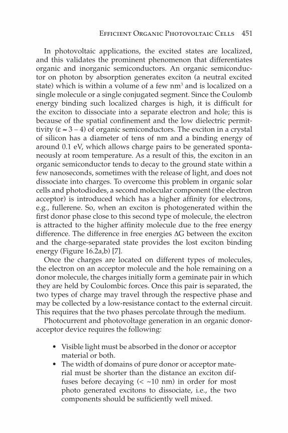
In photovoltaic applications, the excited states are localized, and this validates the prominent phenomenon that differentiates organic and inorganic semiconductors. An organic semiconduc-tor on photon by absorption generates exciton (a neutral excited state) which is within a volume of a few nm3 and is localized on a single molecule or a single conjugated segment. Since the Coulomb energy binding such localized charges is high, it is diffi cult for the exciton to dissociate into a separate electron and hole; this is because of the spatial confi nement and the low dielectric permit-tivity (ε ≈ 3 – 4) of organic semiconductors. The exciton in a crystal of silicon has a diameter of tens of nm and a binding energy of around 0.1 eV, which allows charge pairs to be generated sponta-neously at room temperature. As a result of this, the exciton in an organic semiconductor tends to decay to the ground state within a few nanoseconds, sometimes with the release of light, and does not dissociate into charges. To overcome this problem in organic solar cells and photodiodes, a second molecular component (the electron acceptor) is introduced which has a higher affi nity for electrons, e.g., fullerene. So, when an exciton is photogenerated within the fi rst donor phase close to this second type of molecule, the electron is attracted to the higher affi nity molecule due to the free energy difference. The difference in free energies ΔG between the exciton and the charge-separated state provides the lost exciton binding energy (Figure 16.2a,b) [7].
Once the charges are located on different types of molecules, the electron on an acceptor molecule and the hole remaining on a donor molecule, the charges initially form a geminate pair in which they are held by Coulombic forces. Once this pair is separated, the two types of charge may travel through the respective phase and may be collected by a low-resistance contact to the external circuit. This requires that the two phases percolate through the medium.
Photocurrent and photovoltage generation in an organic donor-acceptor device requires the following:
• Visible light must be absorbed in the donor or acceptor material or both.
• The width of domains of pure donor or acceptor mate-rial must be shorter than the distance an exciton dif-fuses before decaying (< ~10 nm) in order for most photo generated excitons to dissociate, i.e., the two components should be suffi ciently well mixed.
452 Solar Cell Nanotechnology
• Both phases should form continuous percolating net-works that connect the bulk of the fi lm to the electrodes. The electrodes should be electronically different, such that electrons are preferentially collected at one and holes at the other, in order to provide a direction for the photocurrent. Such selectivity can be achieved using one high and one low work function electrode.
Becquerel [8] discovered the photovoltaic effect, i.e., light-induced voltage in 1839 when he shed light onto an AgCl electrode in an electrolyte solution. The fi rst solid-state solar cell was demonstrated
(Donar)
LUMO
LUMO
HOMO
(a)
(b)
HOMO
DECS
DECS
DG
DEe
Eg
(Acceptor)
1D*1A*
3A*
[D+–A–] D+, A–
3D*
Exc
ited
stat
e de
cay
Gem
inat
ere
com
bina
tion
Non
-gem
inat
ere
com
bina
tion
Figure 16.2 a) Schematic diagram showing an organic solar cell based on heterojunction between the electron donor and electron acceptor. b) State diagram of the total energy of the states involved in charge pair generation.
Efficient Organic Photovoltaic Cells 453
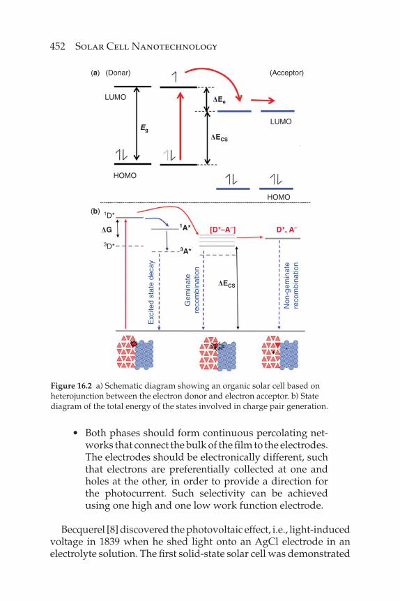
by Fritts in 1883 by depositing a thin layer of Au on Se semicon-ductor, which served as the light absorber to convert photons into electron-hole pairs. The photo-excited charge carriers separated the internal electric fi eld in the Au/Se Schottky junction. Inorganic solar cells even today have light absorption and charge separation as two fundamental processes. Ohl [9] patented modern solar cells in 1946 which were subsequently demonstrated by Chapin, Fuller, and Pearson in 1954 at Bell Laboratories. Figure 16.3 [10] illustrates the principle of their cell which employed a single-crystal Si (sc-Si) wafer for light absorption and a p-n junction for charge separation and had an effi ciency of ~5%. Absorption of photon is through-out the wafer and extends outside the depletion region. So, charge separation makes diffusion of photo-excited charge carried toward the depletion region. As a result of this, the quality of the entire wafer becomes critical in terms of minority carrier lifetime and car-rier mobility for high effi ciency. Contradictory to this, in most of the CMOS devices it is the quality of the surface region that matters most since the operation takes place within a thin layer (<100 nm) of the wafer surface. In spite of the steady improvement in the effi -ciency of solar cells since 1954, the majority of today’s commercial solar cells are very much similar to the Bell Laboratories’ cell, uti-lizing a Si wafer in either single-crystal or polycrystalline form for light absorption and a p-n junction for charge separation.
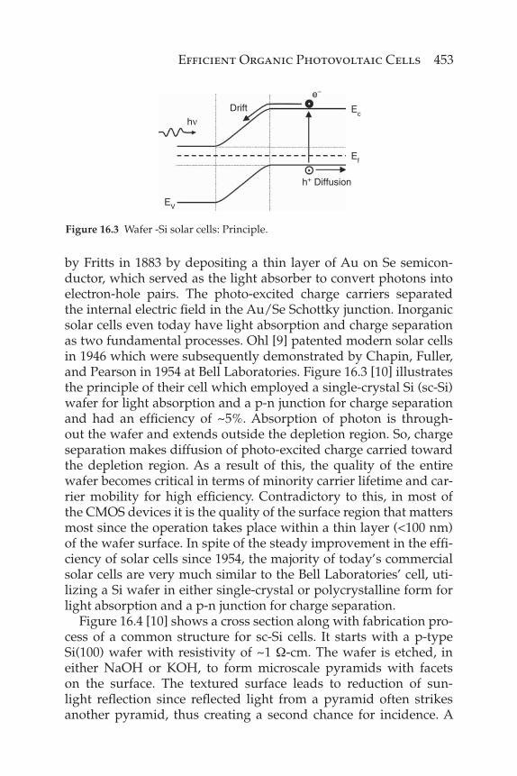
Figure 16.4 [10] shows a cross section along with fabrication pro-cess of a common structure for sc-Si cells. It starts with a p-type Si(100) wafer with resistivity of ~1 Ω-cm. The wafer is etched, in either NaOH or KOH, to form microscale pyramids with facets on the surface. The textured surface leads to reduction of sun-light refl ection since refl ected light from a pyramid often strikes another pyramid, thus creating a second chance for incidence. A
EV
Ef
Echν
Drifte–
h+ Diffusion
Figure 16.3 Wafer -Si solar cells: Principle.

454 Solar Cell Nanotechnology
p-n junction is formed by diffusing n-type dopants, often P, into the front side of the wafer for a typical depth of ~0.5 μm. The back-side electrical contact is formed by reacting a screen-printed Al fi lm and the wafer to form an AlSi compound.
In this cell, the front fi nger contact is also screen printed with an Ag paste. The typical width of the contact fi ngers is ~200 μm, and the separation between two fi ngers is ~3 mm, to maintain a bal-ance between minimum resistance and minimum light shadowing. The fi nal step involves deposition of a transparent material, often SiNx, on the wafer as an antirefl ection coating by plasma-enhanced chemical vapor deposition (PECVD).
Figure 16.5 [10] shows the continual improvement in the effi ciency for various solar cell technologies over the last three decades. As of now, the reported effi ciency of sc-Si cells has reached 24.7%, while that of polycrystalline Si (poly-Si) cells is at 20.3%. The maximum recorded effi ciency for all solar cell technologies is held at 40.8%, obtained with a so-called tandem cell. This cell involves stacking of three p-n junc-tions made of GaxIn1-xAs or GayIn1-yP with different compositions. Each junction has a different bandgap and absorbs light in a certain portion of the solar spectrum. The effi ciency of this cell was measured with a concentrator under 326 Suns. Under one Sun, the reported effi ciency of this triple junction cell is 33.8%. In addition to wafer Si, several thin-fi lm solar cell technologies have also been commercial-ized, including Si in either amorphous (a-Si) or microcrystalline (μc-Si) form and metal chalcogenides (CdTe and CuInxGa1- xSe2(CIGS)). Their record effi ciencies were obtained in the range between 12% and 20%. Though the progress in effi ciencies of these laboratory-size solar cells has been remarkable, the commercial-size cells and modules
AR coating Ag
P-base
(a)
(b)
(c)
(d)
Al
N-emitter
Figure 16.4 Cross-sectional view and fabrication process of single-crystal Si solar cells: (a) Charge separation. Figure shows different processes, i.e., (b) n-emitter diffusion, (c) metallization, and (d) antirefl ection coating.

Efficient Organic Photovoltaic Cells 455
could typically achieve only one-half to two-thirds of these recorded effi ciencies. Eliminating the effi ciency gap is one of the subjects of ongoing research, especially by the solar cell industry.
Figure 16.6 [10] shows the market share of different solar cell technologies in 2007. Poly-Si with 53% has the largest, followed by sc-Si at 33% and all the thin-fi lm technologies at 11% of the market.
16.2 Current Developments in OPVs
The signifi cant advances achieved for Organic Photo Voltaic (OPV) technology are the results of exhaustive development work on four major fronts: (i) clarity in understanding the photon-to-electron
Ribbon-Si 3%CIGS 1%CdTe 6%
a-Si 4%
sc-Si 33%Poly-Si 53%
Figure 16.6 Solar Cell Technologies – Market Scenario in 2007.
Figure 16.5 Current best research-cell effi ciencies versus time for various technologies. (Source: National Renewable Energy Laboratory, 2012, www.nrel.gov)

456 Solar Cell Nanotechnology
conversion mechanism; (ii) development of new materials having tailored energy levels and solubility as required for the end appli-cation; (iii) optimal microstructures in the active layer achieved by new processing techniques; and (iv) new improved devices with novel interfacial layers. In this section, we briefl y review the recent developments pertaining to materials, specially poly-mers, fullerenes and nanomaterials. The main objectives in the fi eld of OPV are achieving high effi ciency, long-term stability and low cost. Low cost can be achieved by combining a low bill of raw materials with high productivity roll-to-roll (R2R) man-ufacturing techniques. It is essential that compared to Si-based solar cells, organic solar cells should be less expensive and eas-ier to manufacture due to lower energy consumption, free from vacuum process, and the possibility of direct patterning during coating. Applications based on organic semiconductors, such as light-emitting diodes and photovoltaic devices, have strict and precise requirements of the layer properties, such as thickness, uniformity and over-layer accuracy. Various printing and coating techniques are applied and developed for the deposition of thin layers of organic semiconductors. Galagan et al. [11] reported a technology for the roll-to-roll production of OPV and also pro-posed further improvements in this technology.
Bulk heterojunction solar cells based on a series of variable alkyl chain length substituted donor–acceptor (D–A) conjugated polymers with thiophene ring and benzenetriazole moiety as the donor and the acceptor, respectively, have been investigated [12]. Evaluation of the optical and electrochemical properties showed that the absorption onsets and the energy levels of the copoly-mers were not dependent of alkyl substitution. D–A copolymers PTBT-DA6, PTBT-DA10 and PTBTDA12 have been successfully investigated in terms of their photovoltaic performances. Among all polymers PTBT-DA10 showed the best performance with a Power Conversion Effi ciency (PCE) of 1.23%. Further optimizations such as using additives and different alkyl-alkoxy chains on the poly-mer backbone can lead to higher PCEs and readily synthesizable PTBT-DA polymers which are exceptional candidates for organic photovoltaics.
A paper presents [13] results for photovoltaic performance obtained from the application of different bulk heterojunction blends onto fl exible polypropylene (PP) substrates for textile applications. A new device which employed a transparent metal

Efficient Organic Photovoltaic Cells 457
cathode (ca. 10 nm LiF/Al) and highly conductive PEDOT:PSS- and Ag-based anode was achieved in this study. These results show that polymer-based solar cell materials and manufacturing techniques are suitable and applicable for fl exible and non-transparent textiles, especially tapes and fi bers, with transparent outer electrodes.
Blankenburg and coworkers [14] reported for the fi rst time extremely promising results in up-scaling coating processes for thin fl exible polymer solar cell (PSC) application. Two func-tional layers for PSC devices, the conducting poly(3,4-ethylene-dioxythiophene):polystyrene sulfonate and the photoactive one (poly-3-hexylthiophene/ [6,6]-phenyl-C61-butyric acid methyl ester), could be successfully prepared by continuous R2R wet coat-ing of low-viscosity solutions and dispersions on ITO-coated PET substrate. It was concluded that BHJ-PSC can be produced with adjustable coating thicknesses on plastic foil using a R2R slot die coating process for the preparation of transparent conducting and photoactive layers.
Two main research and technological areas of development in both organic and inorganic solar cells are the inclusion of plasmonic metal nanoparticles to boost the effi ciency of thin-fi lm solar cells by increasing light absorption, and the incorporation of graphene as transparent conductive electrode to replace indium tin oxide (ITO) fi lms. It was demonstrated that both the plasmon resonance of gold nanoparticles and graphene are valuable approaches to improve performance of both silicon and organic solar cells.
The incorporation of photovoltaics (PVs) into clothing opens up the possibility of having a truly mobile and handy source of energy that can be used for charging batteries for communications equip-ment, monitoring and lighting.
Krebs et al. [15] presented two strategies for incorporation of polymer PVs into clothing. The fi rst strategy involved the simple incorporation of a polymer PV on a polyethyleneterphthalate (PET) substrate directly into the clothing as a structural element. The sec-ond strategy was more elaborate and involved the lamination of a thin layer of polyethylene (PE) onto a textile material followed by plasma treatment and application of a PEDOT electrode onto the textile material. Subsequent screen printing of the active material and evaporation of the fi nal electrode completed the device as a polymer PV that is fully integrated into the textile material. These strategies of the incorporation of polymer PVs into garments and textiles may fi nd the application in “intelligent clothing.”

458 Solar Cell Nanotechnology
A roll-to-roll process enabling fabrication of polymer solar cells comprising fi ve layers on fl exible substrates is presented by Krebs [16]. While the process effi ciently met all the objectives set out and solves many of the problems currently encountered in attempts to upscale and transfer the polymer solar cell technology to industry, there is a sacrifi ce in performance due to poor light transmission of the PEDOT:PSS-silver grid composite electrode.
Commercially available semiconductor quantum dots have been encapsulated [17] within a poly(methyl, methacrylate) polymer matrix to form a luminescent downshifting layer. It was shown that core/shell semiconductor quantum dots are a strong contender for use in luminescent downshifting on CdTe photovoltaic devices.
Hoth et al. [18] showed that with spray coating technology it is possible to deposit all solution processable layers of organic solar cells. With this technology, the hole transporting layer poly(3,4-ethylene dioxythiophene) doped with polystyrene sulphonic acid (PEDOT:PSS) can also be deposited. It was demonstrated that a fully-sprayed coated device with 2.7% PCE can be developed.
A series of ester functionalized [19] polythieno[3,4-b] thiophene derivatives (P1–P3) were prepared by Stille cross-coupling polym-erization. From P1 to P3, the bandgap becomes wider and the HOMO energy level becomes lower with increasing the content of the thiophene-3,4-dicarboxylate moiety in the polymer backbone. Though the fi nal PCE of the prepared OPV devices based on the three copolymers is not high (the best is 1.02%), a high Voc up to 0.71 V can be achieved, suggesting that incorporation of thiophene-3,4-dicarboxylate moiety into the polythieno[3,4 b] thiophene back-bone is a feasible way to gain high voltage OPVs.
Kroon et al. [20] reported a new class of quinoxaline- and pyridopyr-azine-based polymers for solution-processable photovoltaics. Three new TQ1 (this polymer, known as poly[2,3-bis(3-(octyloxy)phenyl)qui- noxaline-alt-thiophene]) derivatives were developed in which the acceptor structure has been modifi ed. It was demonstrated that small structural alterations on the original TQ1 structure results in sig-nifi cantly different electronic properties. The synthesis route is robust towards changes in side-chain chemistry, other heteroatoms, as well as partial fl uorination. Thus, in principle, a vast library of polymers such as TQ1 can readily be generated that will all have different prop-erties. The polymers synthesized resulted in moderate to substantial photovoltaic performance. In this study, devices based on TQ-8A dis-played an improved fi ll factor when compared to TQ1-based devices.

Efficient Organic Photovoltaic Cells 459
Two semiconducting copolymers [21] based on porphyrin compounds, poly[9,9-dioctylfl uorene-co-5,15-bis(hexoxybenzyl)-10,20-bis(benzo-4-yl)porphyrin] (PFPor) and poly[9-(heptadecan-9-yl)carbazole-co-5,15-bis(hexoxybenzyl)-10,20-bis(benzo-4-yl)porphyrin] (PCPor), were used as organic photovoltaic materials. The two polymers did not exhibit exceptionally high PCEs if absorp-tion properties of these materials were reinforced by enlarging a con-jugation length. However, by improving charge transferred property through adopting effi cient spacer materials in polymer backbones, it is expected that new high-performance organic photovoltaic materials could be developed. Materials based on phthalimide were successfully synthesized through the Suzuki coupling reaction for the OPVs. Although, the two polymers did not exhibit unusually high PCEs if phthalimide derivatives with reinforced electron affi n-ity due to introducing electron withdrawing functional groups, are adopted in polymer backbones, and expected that new high perfor-mance organic photovoltaic materials could be developed.
A donor-acceptor type low bandgap [22] conjugated polymer that was composed of carbazole and 4,7-dithiazolylbenzothiadiazole (DTzBT), i.e., Poly [N-9′-heptadecanyl-2,7-carbazole-alt-5,5-(4′,7′-di-2-thiazol-2′,1′,3′-benzothiadiazole)](PCDTzBT)] (PCDTzBT), was synthesized through the Suzuki coupling polymerization for organic photovoltaics. These copolymers exhibited low bandgaps of 1.85 eV and well-balanced HOMO and LUMO energy levels of −5.54 and −3.65 eV, respectively. Although the low molecular weight prohib-ited PCDTzBT from having as high a PCE value as PCDTBT, it is expected that PCDTzBT will improve the photovoltaic properties of devices by optimizing polymerization conditions and with the intro-duction of alkyl chains.
A solution-processable [23], low-cost, and environmentally-friendly bulk heterojunction photovoltaic device based on ZnO nanoparticles/P3HT hybrid material was developed by Li and coworkers. The performance of the solar cells can be signifi cantly improved through interfacial modifi cation with the semiconduct-ing liquid crystal ligands.
In their work, Li and coworkers [24] intramolecularly incorporated the mesogenic cyanobiphenyl to photo-cross-linkable polythiophenes for the purpose of highly stable and ordered liquid-crystalline conju-gated materials. A clear advantage of the photo-crosslinking strategy is that crosslinking can be decoupled from thermal annealing. This valuable feature for BHJ solar cells require some annealing to achieve

460 Solar Cell Nanotechnology
optimum nanomorphology before crosslinking, and freeze the opti-mum morphology to preserve long-term performance.
A series of soluble poly(perylene diimide)s [25] were synthesized and evaluated in organic photovoltaic cells. These polymers were synthesized through the polycondensation of perylene-3,4,9,10-tet-racarboxylic dianhydride (PTCDA) with a number of poly(ethylene glycol) (PEG)- or poly(propylene glycol) (PPG)-based diamine comonomers. These new polymers exhibit good performance in solution processable applications as stable electron-conductive lay-ers with large light absorbtivities.
Synthesis of conjugated polymers [26] bearing indacenodithio-phene and cyclometalated platinum (II) units and their application in organic photovoltaics was reported by Liao et al. The absorption bands of the metal-based polymers were signifi cantly red-shifted relative to those of the metal-free polymers. Notably, the higher performance of Pt-containing polymers device is not attributed to the triplet contribution, but the signifi cant red–shifted (80–90 nm) absorption bands of the Pt-containing polymers, resulting in supe-rior overlap with the solar spectrum which was consistent with the current. When designing such conjugated polymers, one should take into consideration the negative effects of large dihedral angles, which disrupt intermolecular interactions and charge mobility.
A novel copolymer [27] system was developed with high crystal-linity and photocrosslinkable building blocks for p–p intermolecular interactions that has, an alternating copolymer of liquid-crystalline nature and heat/solvent resistance characteristics. By copolymeriza-tion of 2,5-bis(3- bromododecylthiophen-2-yl)thieno[3,2-b]thiophene (BbTTT) monomer with thiophene and thieno[3,2-b]thiophene via Stille reaction, two novel copolymers, PBbTTT-T and PBbTTT-TT, were synthesized.
You and coworkers [28] reported the development of a high-performance low bandgap polymer (bandgap of 1.4 eV), poly[2,7-(5,5-bis-(3,7-dimethyloctyl)-5H-dithieno[3,2-b:20,30-d]pyran)-alt-4,7-(5,6-difl uoro-2,1,3-benzothia diazole)] with a bandgap of 1.38 eV, high mobility and deep HOMO. As a result, a single-junction device shows high external quantum effi ciency of more than 60% and spectral response that extends to 900 nm, with power conversion effi ciency of 7.9%. The polymer can be used to process tandem solar cell from solu-tion with certifi ed 10.6% power conversion effi ciency under standard reporting conditions. This is the fi rst certifi ed polymer solar cell effi -ciency reported beyond 10%.

Efficient Organic Photovoltaic Cells 461
16.2.1 Development of Low Optical Gap Materials
Number of strategies have been pursued to extend the absorp-tion range of donor polymers for OPV. It includes extension of the conjugation length of π-conjugated segments, i.e. replacing phenyl rings with thiophene rings which facilitate to planarize the poly-mer backbone through a reduced steric effect or by using a bridging atom to planarize neighboring monomers [29]. It reduces optical gap further by enabling the formation of π-stacked aggregates [30]. Another approach deals with varying heteroatoms in the conju-gated backbone, for e.g., replacing the sulphur atom in polythio-phene with selenium, which leads to a lowered LUMO energy but unchanged HOMO, due to the infl uence of the heteroatom on the LUMO in this molecule [31]. The recently used route involves com-bining electron rich (e.g., thiophene,pyridine,pyrrole containing) and electron poor (e.g., benzothiadiazole [BT]) units in the poly-mer backbone in a ‘push-pull’ structure. The HOMO of this copoly-mer is dominated by the HOMO of the electron defi cient unit and the LUMO by that of the electron rich unit. This strategy is widely adopted because of large range of ‘push’ and ‘pull’ units that can be used and the ability to control copolymer HOMO and LUMO ener-gies independently. Remarkable advances in OPV effi ciency were made using push-pull copolymers based on dithiophene - BT struc-tures [32], carbazole – BT structures [33], dithienobenzene - modi-fi ed BT structures [34] diketopyrrolopyrrole - thiophene structures [35] (Fig. 16.7) [7].
In the case of fullerenes there is weak optical absorption in the visible area on account of the high symmetry of the C60 cage and resulting symmetry forbidden optical transitions. This defect in can be enhanced by replacing the symmetric C60 cage with one of lower symmetry such as C70which leads to strong blue-green absorp-tion by C70 fullerenes and for this reason they are now widely used in combination of low gap polymers to complement the polymer absorption and span the visible spectrum.
16.2.2 Designing of Higher IP Polymers and Lower EA Acceptors
The push-pull copolymer approach is useful in designing poly-mers with lowered HOMO energy (Voc) since it allows control of the polymer HOMO and LUMO separately. It is also reported that

462 Solar Cell Nanotechnology
push-pull polymers may allow charge pair separation at a lower value of ΔG than other classes of polymers [36].
Other approaches to push down the polymer HOMO include sub-stitution of bridging carbon atoms by the more electronegative silicon [34] and building torsion into the polymer backbone. However, the latter approach has the negative effect of increasing the optical gap.
Another successful route to higher Voc is achieved by reduc-ing the fullerene electron affi nity with the addition of more side chains to derivatives such as PCBM [35], the indene-fullerene [36], and also to metal hydride occupied endohedral fullerenes [37]. This approach has produced excellent results with the crystalline polymer P3HT but has not yet succeeded with any amorphous polymer. The possible reasons are thought to be the inferior microstructure, and consequently transport, formed by the amorphous fullerene adduct and a possible effect on charge generation due to the reduced ΔG [38].
P3HT
PCPDTBT
PCDTBT
PTB7
DPPTT
ICBA
tris-PCBM
bis-PCBM
PCBM
(a) (b)
Figure 16.7 Chemical structures of the polymers, P3HT, PCPDTBT, PCDTBT, PTB7 and a DPP-co-thienothiophene polymer (without side chains for clarity). (b) Chemical structures of the fullerenes, adducts of PCBM and indene fullerene (ICBA).
Efficient Organic Photovoltaic Cells 463
16.2.3 Control of Blend Microstructure
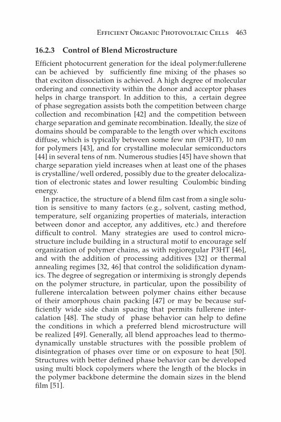
Effi cient photocurrent generation for the ideal polymer:fullerene can be achieved by suffi ciently fi ne mixing of the phases so that exciton dissociation is achieved. A high degree of molecular ordering and connectivity within the donor and acceptor phases helps in charge transport. In addition to this, a certain degree of phase segregation assists both the competition between charge collection and recombination [42] and the competition between charge separation and geminate recombination. Ideally, the size of domains should be comparable to the length over which excitons diffuse, which is typically between some few nm (P3HT), 10 nm for polymers [43], and for crystalline molecular semiconductors [44] in several tens of nm. Numerous studies [45] have shown that charge separation yield increases when at least one of the phases is crystalline/well ordered, possibly due to the greater delocaliza-tion of electronic states and lower resulting Coulombic binding energy.
In practice, the structure of a blend fi lm cast from a single solu-tion is sensitive to many factors (e.g., solvent, casting method, temperature, self organizing properties of materials, interaction between donor and acceptor, any additives, etc.) and therefore diffi cult to control. Many strategies are used to control micro-structure include building in a structural motif to encourage self organization of polymer chains, as with regioregular P3HT [46], and with the addition of processing additives [32] or thermal annealing regimes [32, 46] that control the solidifi cation dynam-ics. The degree of segregation or intermixing is strongly depends on the polymer structure, in particular, upon the possibility of fullerene intercalation between polymer chains either because of their amorphous chain packing [47] or may be because suf-fi ciently wide side chain spacing that permits fullerene inter-calation [48]. The study of phase behavior can help to defi ne the conditions in which a preferred blend microstructure will be realized [49]. Generally, all blend approaches lead to thermo-dynamically unstable structures with the possible problem of disintegration of phases over time or on exposure to heat [50]. Structures with better defi ned phase behavior can be developed using multi block copolymers where the length of the blocks in the polymer backbone determine the domain sizes in the blend fi lm [51].

464 Solar Cell Nanotechnology
Organic/inorganic hybrid structures seem to be a most effi cient route to the control of microstructure, since a rigid and stable inor-ganic framework can be built [52]. For the control of three-dimensional phase structure, the vertical segregation of phases within the blend fi lm should be desirably controlled since this may assist in electrode selectivity and in directing the photocurrent. Other approaches include the choice of electrodes combined with post deposition processing [53] and methods to apply different successive layers from solution [54].
A huge amount of research has been conducted into microscopic and combined microscopic/spectroscopic structural probes includ-ing AFM, TEM, XRD, SE, Raman, and PET due to the complexity of blend fi lm microstructure and the diffi culty of determining structure at nm length scales.
The new photoactive materials are the need of the hour for PV devices with longer service lifespan. The main objectives to be achieved are the design and development of organic semiconduc-tors with improved photochemical stability and blend formulations with greater robustness under heating.
16.3 Economics of Solar Energy
Figure 16.8 [55] depicts PV production from 1990–2010, showing the distribution by geographical area (based on reports from PV News,
Estimatedproduction
2009
0
10
20
30
40
50
60
70
Estimatedproduction
2009
An
nu
al p
rod
uct
ion
/pro
du
ctio
n c
apac
ity
(GW
)
Plannedcapacity
2009
Plannedcapacity
2010
Plannedcapacity
2012
Plannedcapacity
2015
Rest ofworld
Taiwan
China
Europe
Japan
United states
Figure 16.8 Current and planned production and capacity of photovoltaic cells.

Efficient Organic Photovoltaic Cells 465
1980–2011, GTM Research, San Francisco). This signifi cant and excep-tional growth of the technology despite the sluggish world economy bolsters the fact that PV is truly a “real” business now, proving itself as a competitor in the electricity sector, and is expected to exhibit substantial annual growth in capacity, production, and installations in coming years.
Interest in rooftop application (Figure 16.9) [56] started in the USA in the late 1970s. Japan took over the running in the mid-1980s with the construction of a test bed for over 200 residential systems on Rokko Island in 1986. After several years of evaluating techni-cal issues related to their grid connection, a subsidised installa-tion program was launched by the Japanese government in 1993. By the end of 1999, over 20,000 rooftop photovoltaic systems had been installed in urban areas of Japan, with a massive 1.5 million installed during 2010.
It is a well known fact that the ultimate photovoltaic technol-ogy needs to be highly effi cient, low cost, and environmentally friendly. It is also expected that depending upon applications, technology should meet additional requirements such as fl exibil-ity, portability, etc. It can now be concluded that nanomaterials-based photovoltaics have the potency to address these needs, and with the enormous efforts being made across the globe, signifi cant progress is expected in the future. Lee in his review on the current status and projected advancement of concentrated photovoltaics (CPV) concluded that utilizing larger cells at higher concentrations
Solar panelroof top
Figure 16.9 One of the houses of Europe showing PVs installed on its roof.

466 Solar Cell Nanotechnology
would provide greater opportunities for reducing the net cost of ownership while increasing the production of electricity. The ther-mal management in CPV lowers the cost of ownership per watt of electricity generated, mainly through improving two param-eters: 1) effi ciency and 2) reliability. As per the detailed analysis of the future of photovoltaics using the learning curve, electricity from PV can become competitive between 2015 and 2040. It can also be highlighted that not investing in PV is much riskier than promoting the diffusion of PV. In Europe, solar energy is the fast-est growing energy technology and PV farms are integrated in housing. As a matter of fact, the production of solar cells and PV systems have doubled every two years since 2002, yet solar elec-tricity covered only 0.26% of EU electricity consumption in 2008. Southern EU countries have enormous potential for solar energy due to increased sunshine. Solar energy may potentially cover up to 12% of EU’s energy demand by 2020.
The turnover of PV energy was estimated at EUR 10 billion in 2007. Assuming an average PV system cost of 2.5 €/W, the global annual revenue can be estimated at €44 billion in 2010. The European Photovoltaic Industry Association projected this revenue to increase to €200 billion for an annual market size of around 135 GWs, provided that some cost reduction targets are achieved.
The cost per kW is still considered high (around 2.5 €/W), and higher than the conventional energy production in the EU. However the downward trend in cost observed in the last few years is mainly due to increasing effi ciency. As per the forecast of the European Photovoltaic Energy Platform, PV energy may become competitive in a limited and selected group of markets by 2013 and across the entire EU by 2020.
16.3.1 Scenario in US
As per the report of Solar Energy Industries Association, USA, the US now has over 6,400 MWs of installed solar electric capacity, enough to power more than 1 million average American house-holds. The average cost of a completed PV system has dropped by 33 percent in the third quarter of 2012 compared to the beginning of 2011. The average price of a solar panel has declined by 58 per-cent since the fi rst quarter of 2011. As the solar industry grows, its impact on the economy in the US will be apparent. The increase in value of solar installations has positively impacted the US economy.

Efficient Organic Photovoltaic Cells 467
In 2011, solar installations were valued at $8.4 billion, compared to $6 billion in 2010.
16.3.2 Solar Potential in India
India is blessed with rich solar energy resource. The average inten-sity of solar radiation received on India is 20 MW/km square (megawatt per kilometer square). With a geographical area of 3.287 million km square, this is estimated to 657.4 million MW. However, theoretically, a mere 12.5% of the total land area amounting to 0.413 million km square can be used for solar energy installations. As per the estimation, 10% use of this area can result in the avail-able solar energy to 8 million MW per year. However, in India the effi ciency of conversion of solar energy to useful energy is low. As per the order of the Central Electricity Regulatory Commission, the life of a solar PV plant has been accounted for 25 years, and accordingly the tariff has been calculated for 1MW solar PV power projects over a period of 25 years. The cost of one unit of solar elec-tricity has been calculated based on this assumption. Accordingly, the tariff leveled on solar energy has been decided as INR 15.39 by the regulatory commission [57]. Similarly, the cost of electricity over a period of 25 years generated by solar thermal power projects has been calculated. The tariff leveled on solar energy by the Solar Thermal Power Project, therefore, has been decided as INR 15.04 by the regulatory commission based on that assumption [57]. As of now, photovoltaic effi ciency and manufacturing costs have not reached the point where photovoltaic power generation can com-pete with conventional coal-, gas-, and nuclear-powered facilities. As per the current estimates, the cost of solar power is approxi-mately four times that of conventionally (coal-based thermal power station) produced power. There are various factors that are affecting the cost of production and distribution of conventional electrical power. Due to the wide range of these variables, some applications of photovoltaic power are becoming economically superior to con-ventional systems.
16.3.3 Global Solar Cell Demand
Figure 16.10 [58] presents data about when certain countries have reached and will reach grid parity. It shows, for example, that coun-tries with higher electricity prices, such as Germany, Denmark, Italy,

468 Solar Cell Nanotechnology
Spain and parts of Australia have already reached socket parity, (defi ned here as the point where a household can make 5% or more return on investment in a PV system just by using the energy gener-ated to replace household energy consumption) while countries like Japan, France, Brazil and Turkey are expected to reach it by 2015.
16.4 Conclusions and Future Trends in Photovoltaic
Conjugated polymers offers unique opportunity to combine the opto-electronic properties of semiconductors along with the mechanical properties and have processing advantages of polymers. As discussed throughout this chapter in detail that the optical and electronic char-acteristics of conjugated polymers are primarily dependent on the nature of the molecular conjugation which may be easily designed or tailored via organic synthesis. Currently, the main efforts in the fi eld are focused on the development of conjugated polymers with lower optical bandgap that are solvent-processable and are also reasonably stable at ambient conditions.
The new materials under development are used in conjunction with electron acceptors, such as fullerenes and CNTs, for prepara-tion of functional hybrids which are active layer in BHJ POPV. The
8000.00
0.05
0.10
0.15
0.20
0.25
0.30
0.35
0.40
1000
$/kW
h
1200
125GW 2 3EMEAPotential
residentialPV market
ASOC AMER
1400 1600 1800
kWh/kW/year
2000
2012LCOE
2015LCOE
3 Hawaii
Denmark More sun
Germany1
1
1
1
1
1 1
13
22
2
2
2
2 2
2
3
3
33
1
31
3
JapanUnited Kingdom
South Korea
France
ItalySpain
Brazil Australia
California
Israel
Turkey
North IndiaNew Jersey
Canada
Russia
Argentina
North China
Indonesia
SouthChina South India
Saudi Arabia
MexicoTexas
Figure 16.10 Depiction of residential PV price parity-size; bubbles indicate market size.

Efficient Organic Photovoltaic Cells 469
performance of the active layer depends not only on the structure of the different components but also on their spatial organization at the nano- to mesoscales. The morphology determined by interfa-cial and intermolecular interactions between the components may or may not promote the desired performance of the active layer. While morphology performance relations have been thoroughly investigated in fullerene-based hybrids, the effect of CNTs on the polymer-fullerene system is relatively less studied. The inherent structural and morphological heterogeneity of as-produced CNT powders, and the sensitivity of the polymer- CNT system to pro-cessing conditions, contribute to the wide variations in the reported observations and sometimes lead to misleading and controversial conclusions. Furthermore, the fundamental physics of charge trans-fer and charge transport between conjugated polymers and CNT as well as the self-assembly and phase morphology of conjugated polymers-CNT hybrids is still not understood thoroughly. More precisely, it is not yet clear which type of CNT, under which condi-tions, can be used as an interface under what conditions for excition dissociation, charge transporters (holes or electrons), or contribute indirectly to the self-organization of the conjugated polymer layer. The progress and research that has been accomplished over the last decade in regulating the structure and properties of CNT will become the basic guidelines for researchers to further design and carry out well-focused experiments towards signifi cant progress in understanding the fundamentals of optoelectronic behavior in polymer-CNT hybrids. The development of particular processing pathways each adequate for a different end product, coupled with progress in characterization techniques of the resulting hybrids, is expected to signifi cantly improve the properties and the conse-quential performance of CNT-based POPV. The future of conju-gated polymers CNT hybrids as active materials in POPV seems to be exceptionally bright but will certainly depend on the pace of progress in parallel areas of fundamental research and design of technologically feasible solutions for structural engineering at the nano- to the mesoscale of CNT-conjugated polymers hybrids.
PV systems are expensive and still need market support to compete with low-cost conventional electricity supply. The main research challenge and focus are therefore associated with sig-nifi cantly reducing costs, for the modules themselves but also for balance-of-system (BOS) costs, including in particular the invert-ers used for grid connection. Increase in conversion effi ciency of

470 Solar Cell Nanotechnology
these modules is another priority. Array mounting costs refl ects the total module area of the system and thus BOS costs can be rela-tively reduced if effi ciencies are increased. For novel but potentially extremely low-cost dye and plastic cells, there is a need to increase effi ciency and develop designs with long-term stability. The big-gest challenges to both dye and polymer cells are there tendency to degrade on exposure to ultraviolet radiation, atmospheric humid-ity and oxygen. Thin-fi lm cell designs as discussed above are well developed; now the primary research challenge for these designs is to develop better and lower cost production technologies. The large area uniformity of deposition in this type of cell is particularly noteworthy because nonuniformity results in losses due to cell mis-match which can signifi cantly degrade their performance.
There is an increasing need for accurate yield prediction tools with the growth of PV market as potential purchasers of such sys-tems would be extremely interested in understanding more pre-cisely the economics of technology. In the early stages of the growth of grid-connected PV, purchasers might not be concerned with the fi nancial aspects, but later on as the market matures this trend will certainly change. In fact, accurate and easy-to-use yield estimation tools are required, and research is underway in many laboratories to address this issue. It is predicted that PV will make a signifi cant contribution to the electricity supply in the long term. In a country like the UK which has a modest solar resource, estimations show that widescale deployment of PV on existing roofs could generate a substantial proportion of electricity needs.
Researchers have shown that very high performance, space-type cells could be combined with solar concentrators to produce cost-effective electricity. There are also designs available in which fl uo-rescence is being used to capture and concentrate the light falling on a window to its edge, where it can be converted effi ciently, in part because of its narrowband spectrum.
Internal energy storage may also be envisioned in future solar cell materials, e.g., analogous to a photoelectrochemical solar cell (PEC) with internal storage. Various battery technologies, e.g., metal hydrides, and nanotechnologies could represent some of many possible ways of increasing the energy storage density. Future solar cell materials may also be envisioned as thin laminate or paint layers suitable for application by paint brush or spray. However, there is still a need for “intelligent design.” To attain dream of low cost, highly effi cient and robust PVs technology, dedicated efforts

Efficient Organic Photovoltaic Cells 471
are required to provide the technical expertise, resources, creativ-ity and innovation. Current trends indicate that photovoltaic-based electricity will defi nitely prosper and lead to the Age of Neoteric Energy and beyond.
References
1. A. Jäger-Waldau, PV Status Report 2003, European Commission, EUR 20850 EN, 2003.
2. A.J. Heeger, Angewandte Chemie International Edition, Vol. 40, 2591–2611, 2001. 3. A.G. MacDiarmid, Angewandte Chemie International Edition, Vol. 40, 2581–2590,
2001. 4. H. Shirakawa, Angewandte Chemie International Edition, Vol. 40, 2574–2580,
2001. 5. C.K. Chiang, C.R. Fincher, Jr., Y.W. Park, A.J. Heeger, H. Shirakawa, E.J. Louis,
S.C. Gau, and A.G. MacDiarmid, Physical Review Letters, Vol. 39, 1098–1101, 1977.
6. J.H. Burroughes, D.D.C. Bradley, A.R. Brown, R.N. Marks, K. Mackay, R.H. Friend, P.L. Burns, and A.B. Holmes, Nature, Vol. 347, 539–541, 1990.
7. J. Nelson, Materials Today, Vol. 14, 10, 462-470, 2011. 8. E. Becquerel, Comptes Rendus, Vol. 9, 561–567, 1839. 9. R.S. Ohl, and L. Silver, Light-Senstive Electric Device, USPTO, 2,402,662. 10. M. Tao, The Electrochemical Society Interface, Vol. 17, 4, 30-35, 2008.11. Y. Galagan, I.G. de Vries, A.P. Langen, R. Andriessen, W.J.H. Verhees,
S.C. Veenstra, and J.M. Kroon, Chemical Engineering and Processing: Process Intensifi cation, Vol. 50, 454–461, 2011.
12. D. Baran, A. Balan, T. Stubhan, T. Ameri, L. Toppare, and C.J. Brabec, Synthetic Metals, Vol. 162, 2047–2051, 2012.
13. A. Bedeloglu, A. Demir, Y. Bozkurt, and N.S. Sariciftci, Synthetic Metals, Vol. 159, 2043–2048, 2009.
14. L. Blankenburg, K. Schultheis, H. Schache, S. Sensfuss, and M. Schrödner, Solar Energy Materials and Solar Cells, Vol. 93, 476–483, 2009.
15. F.C. Krebs, M. Biancardo, B. Winther-Jensen, H. Spanggard, and J. Alstrup, Solar Energy Materials and Solar Cells, Vol. 90, 1058–1067, 2006.
16. F.C. Krebs, Organic Electronics, Vol. 10, 761–768, 2009.17. S.D. Hodgson, W.S.M. Brooks, A.J. Clayton, G. Kartopu, V. Barrioz, and S.J.C.
Irvine, Nano Energy, Vol. 2, 21–27, 2013.18. C.N. Hoth, R. Steim, P. Schilinsky, S.A. Choulis, S.F. Tedde, O. Hayden, and
C.J. Brabec, Organic Electronics, Vol. 10, 587–593, 2009.19. X.-L. Hu, L.-J. Zuo, Y.-X. Nan, M. Helgesen, O. Hagemann, E. Bundgaard,
M.-M. Shi, F.C. Krebs, and H.-Z. Chen, Synthetic Metals, Vol. 162, 2005–2009, 2012.
20. R. Kroon, R. Gehlhaar, T.T. Steckler, P. Henriksson, C. Müller, J. Bergqvist, A. Hadipour, P. Heremans, and M.R. Andersson, Solar Energy Materials and Solar Cells, Vol. 105, 280–286, 2012.

472 Solar Cell Nanotechnology
21. J.Y. Lee, H.J. Song, S.M. Lee, J.H. Lee, and D.K. Moon, European Polymer Journal, Vol. 47, 1686–1693, 2011.
22. J.Y. Lee, K.W. Song, H.J. Song, and D.K. Moon, Synthetic Metals, Vol. 161, 2434–2440, 2011.
23. F. Li, W. Chen, K. Yuan, and Y. Chen, Organic Electronics, Vol. 13, 2757–2762, 2012.
24. X. Li, L. Chen, Y. Chen, F. Li, and K. Yao, Organic Electronics, Vol. 13, 104–113, 2012.
25. Z. Liang, R.A. Cormier, A.M. Nardes, and B.A. Gregg, Synthetic Metals, Vol. 161, 1014–1021, 2011.
26. C.-Y. Liao, C.-P. Chen, C.-C. Chang, G.-W. Hwang, H.-H. Chou, and C.-H. Cheng, Solar Energy Materials and Solar Cells, Vol. 109, 111–119, 2013.
27. S.Y. Nam, E.Y. Park, T.-D. Kim, S. Cho, J.-G. Park, and K.-S. Lee, Current Applied Physics, Vol. 11, e44-e48, 2011.
28. J. You, L. Dou, K. Yoshimura, T. Kato, K. Ohya, T. Moriarty, K. Emery, C.-C. Chen, J. Gao, G. Li, and Y. Yang, Nature Communication, Vol. 4, 1446, 2013.
29. D. Mühlbacher, M. Scharber, M. Morana, Z. Zhu, D. Waller, R. Gaudiana, and C. Brabec, Advanced Materials, Vol. 18, 2884–2889, 2006.
30. C.J. Brabec, M. Heeney, I. McCulloch, and J. Nelson, Chemical Society Reviews, Vol. 40, 1185–1199, 2011.
31. M. Heeney, W. Zhang, D.J. Crouch, M.L. Chabinyc, S. Gordeyev, R. Hamilton, S.J. Higgins, I. McCulloch, P.J. Skabara, D. Sparrowe, and S. Tierney, Chemical Communications, Vol. 0, 5061–5063, 2007.
32. J. Peet, J.Y. Kim, N.E. Coates, W.L. Ma, D. Moses, A.J. Heeger, and G.C. Bazan, Nat Mater, Vol. 6, 497–500, 2007.
33. S.H. Park, A. Roy, S. Beaupre, S. Cho, N. Coates, J.S. Moon, D. Moses, M. Leclerc, K. Lee, and A.J. Heeger, Nat Photon, Vol. 3, 297–302, 2009.
34. Y. Liang, Z. Xu, J. Xia, S.-T. Tsai, Y. Wu, G. Li, C. Ray, and L. Yu, Advanced Materials, Vol. 22, E135-E138, 2010.
35. H. Bronstein, Z. Chen, R.S. Ashraf, W. Zhang, J. Du, J.R. Durrant, P. Shakya Tuladhar, K. Song, S.E. Watkins, Y. Geerts, M.M. Wienk, R.A.J. Janssen, T. Anthopoulos, H. Sirringhaus, M. Heeney, and I. McCulloch, Journal of the American Chemical Society, Vol. 133, 3272–3275, 2011.
36. T. Clarke, A. Ballantyne, F. Jamieson, C. Brabec, J. Nelson, and J. Durrant, Chemical Communications, Vol. 0, 89–91, 2009.
37. E. Wang, L. Wang, L. Lan, C. Luo, W. Zhuang, J. Peng, and Y. Cao, Applied Physics Letters, Vol. 92, 033307–033303, 2008.
38. M. Lenes, M. Morana, C.J. Brabec, and P.W.M. Blom, Advanced Functional Materials, Vol. 19, 1106–1111, 2009.
39. Y. He, H.-Y. Chen, J. Hou, and Y. Li, Journal of the American Chemical Society, Vol. 132, 5532–5532, 2010.
40. R.B. Ross, C.M. Cardona, D.M. Guldi, S.G. Sankaranarayanan, M.O. Reese, N. Kopidakis, J. Peet, B. Walker, G.C. Bazan, E. Van Keuren, B.C. Holloway, and M. Drees, Nat Mater, Vol. 8, 208–212, 2009.
41. M.A. Faist, P.E. Keivanidis, S. Foster, P.H. Wöbkenberg, T.D. Anthopoulos, D.D.C. Bradley, J.R. Durrant, and J. Nelson, Journal of Polymer Science Part B: Polymer Physics, Vol. 49, 45–51, 2011.
Efficient Organic Photovoltaic Cells 473
42. J.M. Frost, F. Cheynis, S.M. Tuladhar, and J. Nelson, Nano Letters, Vol. 6, 1674–1681, 2006.
43. J.J.M. Halls, K. Pichler, R.H. Friend, S.C. Moratti, and A.B. Holmes, Applied Physics Letters, Vol. 68, 3120–3122, 1996.
44. R.R. Lunt, J.B. Benziger, and S.R. Forrest, Advanced Materials, Vol. 22, 1233–1236, 2010.
45. D. Veldman, O.z. Îpek, S.C.J. Meskers, J.r. Sweelssen, M.M. Koetse, S.C. Veenstra, J.M. Kroon, S.S.v. Bavel, J. Loos, and R.A.J. Janssen, Journal of the American Chemical Society, Vol. 130, 7721–7735, 2008.
46. Y. Kim, S. Cook, S.M. Tuladhar, S.A. Choulis, J. Nelson, J.R. Durrant, D.D.C. Bradley, M. Giles, I. McCulloch, C.-S. Ha, and M. Ree, Nat Mater, Vol. 5, 197–203, 2006.
47. N.C. Cates, R. Gysel, J.E.P. Dahl, A. Sellinger, and M.D. McGehee, Chemistry of Materials, Vol. 22, 3543–3548, 2010.
48. N.C. Cates, R. Gysel, Z. Beiley, C.E. Miller, M.F. Toney, M. Heeney, I. McCulloch, and M.D. McGehee, Nano Letters, Vol. 9, 4153–4157, 2009.
49. C. Müller, T.A.M. Ferenczi, M. Campoy-Quiles, J.M. Frost, D.D.C. Bradley, P. Smith, N. Stingelin-Stutzmann, and J. Nelson, Advanced Materials, Vol. 20, 3510–3515, 2008.
50. S. Bertho, G. Janssen, T.J. Cleij, B. Conings, W. Moons, A. Gadisa, J. D’Haen, E. Goovaerts, L. Lutsen, J. Manca, and D. Vanderzande, Solar Energy Materials and Solar Cells, Vol. 92, 753–760, 2008.
51. R.C. Hiorns, E. Cloutet, E. Ibarboure, A. Khoukh, H. Bejbouji, L. Vignau, and H. Cramail, Macromolecules, Vol. 43, 6033–6044, 2010.
52. J. Boucle, P. Ravirajan, and J. Nelson, Journal of Materials Chemistry, Vol. 17, 3141–3153, 2007.
53. M. Campoy-Quiles, T. Ferenczi, T. Agostinelli, P.G. Etchegoin, Y. Kim, T.D. Anthopoulos, P.N. Stavrinou, D.D.C. Bradley, and J. Nelson, Nat Mater, Vol. 7, 158–164, 2008.
54. T.A.M. Ferenczi, N. Jenny, B. Colin, M.B. Amy, C.-Q. Mariano, M.B. Felix, and D.C.B. Donal, Journal of Physics: Condensed Matter, Vol. 20, 475203, 2008.
55. L.L. Kazmerski, Solar Photovoltaics Technology: No Longer an Outliner, in A. Sayigh Ed., Comprehensive Renewal Energy, Vol. 1, 13-30, 2008.
56. Solar cell- Supplier and Manufacturers A-Z, www.speedace.info/solar_cells.htm (accessed on March, 01, 2013).
57. Renewable Energy Tariff for Financial Year 2011–12, Order-256–2010, Central Electricity Regulatory Commission, India, 2012.
58. A. Jäger-Waldau, “Status and perspectives of thin fi lm photovoltaics,” in A. Bosio and A. Romeo, eds., Thin Film Solar Cells: Current Status and Future Trends, Nova Publisher, New York, ch. 1, pp. 1–24, 2010.