solar cell nanotechnology (tiwari/solar) || two dimensional layered semiconductors: emerging...
TRANSCRIPT
117
Atul Tiwari, Rabah Boukherroub, and Maheshwar Sharon (eds.) Solar Cell Nanotechnology, (117–134) 2014 © Scrivener Publishing LLC
4
Two Dimensional Layered Semiconductors: Emerging Materials
for Solar Photovoltaics
Mariyappan Shanmugam and Bin Yu*
College of Nanoscale Science and Engineering, State University of New York, Albany, New York, USA
Abstract Graphene-like, two-dimensional (2D), lattice-structured transition metal dichalcogenides are layered semiconductors consisting of covalent bonded atomic planes coordinated by van der Waals forces. This chapter presents two important layered semiconductors, molybdenum disulfi de (MoS2) and tungsten disulfi de (WS2), as photoactive material candidates for bulk heterojunction (BHJ) and Schottky barrier solar cells. Development of functional materials by chemical exfoliation and chemical vapor deposi-tion are presented with experimental processing steps. Microstructural and Raman spectroscopic studies were performed on the developed MoS2 and WS2 semiconductors. Fabrication and characterization of functional photovoltaic devices, performance evaluation, electronic transport and interfacial recombination mechanisms in BHJ and Schottky barrier solar cells are presented. Nanofl akes and nanofi lms of 2D-layered semiconduc-tors employed in BHJ and Schottky barrier solar cells emphasize that the absorption limit can be tuned by controlling thickness of the material con-fi rmed by solar cell performance.
Keywords: Layered semiconductors, chemical vapor deposition, solar cell, bulk heterojunction, Schottky barrier, electronic transport, interfacial recombination
*Corresponding author: [email protected]
118 Solar Cell Nanotechnology
4.1 Introduction
Bulk heterojunction (BHJ) solar cells, employing both organic and inorganic semiconductors, show promise in emerging photovol-taic technology due to their improved stability and performance. Titanium dioxide (TiO2) has been widely used as an electron acceptor in bulk BHJ solar cells and has shown promising photoconversion effi ciencies [1–5]. A porous TiO2 nanoparticle-based electron acceptor is preferred for BHJ solar cell application due to the fact that a large amount of surface is required to load a hole-conducting polymer. The porous TiO2 offers a potential opportunity to form heterojunc-tion with polymer hole conductors in a large area to enhance exciton generation and separation. Various nanostructures of TiO2 such as nanoparticles, nanorods and nanotubes have been employed in BHJ solar cells [6–8]. Poly(3-hexylthiophene) (P3HT) is widely used as a hole conductor with TiO2 as an electron acceptor in BHJ solar cell technology. The blend morphology between electron acceptor and hole conductor is an essential factor in determining the charge trans-port, recombination and performance of the BHJ solar cells [9, 10].
Shottky barrier solar cells are relatively simple structures com-pared to heterojunction and multi-junction solar cells and exhibit promising photovoltaic performance. Both p-type and n-type doped semiconductors can be used in Schottky barrier solar cells with a metal of appropriate work function. Bulk and thin fi lms of various semiconductor materials have been employed in Schottky barrier solar cells, and the results have shown the possible potential opportunities of Schottky barrier solar cells in renewable energy technology [11–15]. Allotropes of carbon, a low cost material candi-date compared to expensive bulk and thin-fi lm semiconductors and metals, have recently been employed in Schottky barrier solar cells as metal contact [16–20]. Major disadvantage with conventional semiconductors such as Si, Ge and GaAs are the surface states due to the unsaturated dangling bonds which play a role of recombination centers in solar cells [21–23]. Surface states adversely affect electron lifetime in solar cells by increasing the surface recombination veloc-ity [24]. Semiconductor surface is a critical part in Schottky barrier solar cells at which the barrier for electrons and holes is formed due to the work function difference between semiconductors and metal. Surface states on the semiconductor surface deteriorate the formation of Schottky barrier height, and thus affect the built-in potential at the metal/semiconductor interface. Surface states on a
Two Dimensional Layered Semiconductors 119
semiconductor can be passivated by high-k dielectric materials to enhance the solar cell performance [25, 26]. The surface states on the active semiconductors employed in Schottky barrier solar cell become interfacial states while the metal contact is deposited on the semiconductor. Metal/semiconductor junction with interfacial defect states experience Fermi level pinning which lowers the bar-rier height and hence lowers solar cell performance.
Graphite-like layered semiconductors with two-dimensional (2D) lattice structure belong to transition metal dichalcogenides (TMDs), and have been employed as active semiconductor layers in nano/opto-electronics. Optical properties of the 2D layered semiconduc-tors such as molybdenum disulfi de (MoS2) and tungsten disulfi de (WS2) can be tuned from 1.2 eV to 1.8 eV by changing layer thick-ness. Both direct and indirect bandgap nature can be achieved in 2D layered semiconductors by controlling the number of layers in a stack. Such fl exibility in tuning optical bandgap of the active layer semiconductors offers unique opportunities in opto-electronics and photovoltaic technology. MoS2 and WS2 have recently been studied for nanoelectronics applications [27–30]. Dependency of electrical conductivity, optical bandgap and carrier mobility of 2D layered semiconductors are the major key factors infl uencing them in opto-electronic device applications [31–36].
In this chapter, we present functional 2D layered semiconductor material development and characterization for BHJ and Schottky barrier solar cells. Chemically exfoliated 2D layered semiconductor nanofl akes-based BHJ solar cells and CVD-synthesized, 2D layered semiconductors-based Schottky barrier solar cells are presented. Photovoltaic performance, electron transport and recombina-tion processes at interfaces are studied to demonstrate 2D layered semiconductors as potential candidates for emerging photovoltaic technology.
4.2 Material Synthesis
4.2.1 Chemical Exfoliation
Bulk crystals of 2D layered semiconductors MoS2 and WS2 were used to exfoliate nanofl akes by ultra-sonication using 2-propanol as a solvent. The 2D layered semiconductor crystals were used as purchased from US Research Nanomaterials, Inc. The bulk crystals
120 Solar Cell Nanotechnology
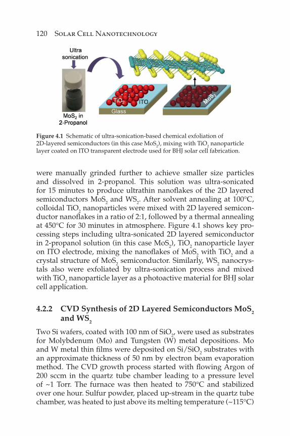
were manually grinded further to achieve smaller size particles and dissolved in 2-propanol. This solution was ultra-sonicated for 15 minutes to produce ultrathin nanofl akes of the 2D layered semiconductors MoS2 and WS2. After solvent annealing at 100°C, colloidal TiO2 nanoparticles were mixed with 2D layered semicon-ductor nanofl akes in a ratio of 2:1, followed by a thermal annealing at 450°C for 30 minutes in atmosphere. Figure 4.1 shows key pro-cessing steps including ultra-sonicated 2D layered semiconductor in 2-propanol solution (in this case MoS2), TiO2 nanoparticle layer on ITO electrode, mixing the nanofl akes of MoS2 with TiO2 and a crystal structure of MoS2 semiconductor. Similarly, WS2 nanocrys-tals also were exfoliated by ultra-sonication process and mixed with TiO2 nanoparticle layer as a photoactive material for BHJ solar cell application.
4.2.2 CVD Synthesis of 2D Layered Semiconductors MoS2 and WS2
Two Si wafers, coated with 100 nm of SiO2, were used as substrates for Molybdenum (Mo) and Tungsten (W) metal depositions. Mo and W metal thin fi lms were deposited on Si/SiO2 substrates with an approximate thickness of 50 nm by electron beam evaporation method. The CVD growth process started with fl owing Argon of 200 sccm in the quartz tube chamber leading to a pressure level of ~1 Torr. The furnace was then heated to 750°C and stabilized over one hour. Sulfur powder, placed up-stream in the quartz tube chamber, was heated to just above its melting temperature (~115°C)
Figure 4.1 Schematic of ultra-sonication-based chemical exfoliation of 2D-layered semiconductors (in this case MoS2), mixing with TiO2 nanoparticle layer coated on ITO transparent electrode used for BHJ solar cell fabrication.
Two Dimensional Layered Semiconductors 121
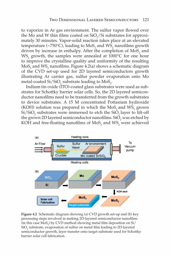
to vaporize in Ar gas environment. The sulfur vapor fl owed over the Mo and W thin fi lms coated on SiO2/Si substrates for approxi-mately 30 minutes. Vapor-solid reaction takes place at an elevated temperature (~750°C), leading to MoS2 and WS2 nanofi lms growth driven by increase in enthalpy. After the completion of MoS2 and WS2 growth, the samples were annealed at 1000°C for one hour to improve the crystalline quality and uniformity of the resulting MoS2 and WS2 nanofi lms. Figure 4.2(a) shows a schematic diagram of the CVD set-up used for 2D layered semiconductors growth illustrating Ar carrier gas, sulfur powder evaporation onto Mo metal-coated Si/SiO2 substrate leading to MoS2.
Indium tin oxide (ITO)-coated glass substrates were used as sub-strates for Schottky barrier solar cells. So, the 2D layered semicon-ductor nanofi lms need to be transferred from the growth substrates to device substrates. A 15 M concentrated Pottasium hydroxide (KOH) solution was prepared in which the MoS2 and WS2 grown Si/SiO2 substrates were immersed to etch the SiO2 layer to lift-off the grown 2D layered semiconductor nanofi lms. SiO2 was etched by KOH and free-fl oating nanofi lms of MoS2 and WS2 were achieved
(a)
(b)
Figure 4.2 Schematic diagram showing (a) CVD growth set-up and (b) key processing steps involved in making 2D-layered semiconductor nanofi lms (in this case MoS2) by CVD method showing metal fi lm deposition on Si/SiO2 substrate, evaporation of sulfur on metal fi lm leading to 2D-layered semiconductor growth, layer transfer onto target substrate used for Schottky barrier solar cell fabrication.
122 Solar Cell Nanotechnology
in KOH solution. Figure 4.2(b) shows key process steps involved in CVD synthesis of 2D layered semiconductor growth and transfer (in this case MoS2 nanofi lm) from SiO2-coated Si substrate and layer transfer after the KOH etch to the target substrate used for Schottky barrier solar cell fabrication. The process steps are the same for WS2 nanofi lm growth and transfer.
4.2.3 Material Characterization
A HORIBA Scientifi c Raman spectrometer with a laser of 514.5 nm excitation wavelength was used to study the MoS2 and WS2 nano-fl akes-coated TiO2 electron acceptor used for the BHJ solar cell fab-rication, as reported in this chapter. A LEO 1550 scanning electron microscope was used to study the thickness and surface morphol-ogy of the 2D layered semiconductor nanofl akes-coated TiO2.
4.3 Photovoltaic Device Fabrication
4.3.1 Bulk Heterojunction Solar Cells
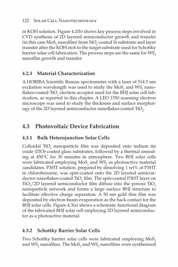
Colloidal TiO2 nanoparticle fi lm was deposited onto indium tin oxide (ITO)-coated glass substrates, followed by a thermal anneal-ing at 450°C for 30 minutes in atmosphere. Two BHJ solar cells were fabricated employing MoS2 and WS2 as photoactive material candidates. P3HT solution, prepared by dissolving 1 wt% of P3HT in chlorobenzene, was spin-coated onto the 2D layered semicon-ductor nanofl akes-coated TiO2 fi lm. The spin-coated P3HT layer on TiO2/2D layered semiconductor fi lm diffuse into the porous TiO2 nanoparticle network and forms a large surface BHJ structure to facilitate effective charge separation. A 50 nm gold thin fi lm was deposited by electron-beam evaporation as the back contact for the BHJ solar cells. Figure 4.3(a) shows a schematic functional diagram of the fabricated BHJ solar cell employing 2D layered semiconduc-tor as a photoactive material.
4.3.2 Schottky Barrier Solar Cells
Two Schottky barrier solar cells were fabricated employing MoS2 and WS2 nanofi lms. The MoS2 and WS2 nanofi lms were synthesized
Two Dimensional Layered Semiconductors 123
by CVD method as explained in Section 4.2.2. The nanofi lms of 2D layered semiconductor MoS2 and WS2 were transferred onto the ITO-coated substrate as the photoactive material for the Schottky barrier solar cell. A 50 nm of Au metal fi lm was deposited by elec-tron-beam evaporation on the 2D layered semiconductor nanofi lms, forming Schottky junction with the nanofi lms. The transparent ITO electrode was used as the front contact of the Schottky barrier solar cell through which the photons incident on the 2D layered semi-conductors. Multiple transfers of nanofi lms were made onto ITO to yield the total active layer thickness of ~200 nm. Figure 4.3(b) shows a schematic diagram of the fabricated Schottky barrier solar cells employing CVD-synthesized 2D layered semiconductor nano-fi lms of MoS2 and WS2.
4.3.3 Device Characterization
The current density-voltage (J-V) characteristics of the fabricated BHJ and Schottky barrier solar cells were measured under both dark and standard AM 1.5 illumination conditions calibrated using a standard silicon solar cell by Agilent B1500A semicon-ductor device analyzer. A Xe arc lamp was used to simulate the AM 1.5 photon fl ux for the J-V characteristic measurements. The external quantum effi ciency (EQE) spectra of the BHJ and Schottky barrier solar cells were measured in the wavelength range of 350 nm ~ 900 nm using a Newport monochromator
Figure 4.3 Schematic of cross sectional views of the fabricated (a) BHJ solar cell employing 2D-layered semiconductor nanofl akes as photoactive materials (in this case MoS2) and (b) Schottky barrier solar cell with layer transferred 2D-layered semiconductor nanofi lm stack (in this case MoS2).
124 Solar Cell Nanotechnology
equipped with the same Xe arc lamp that was used to measure the J-V characteristics of the BHJ solar cells. Capacitance-voltage (C-V) characteristics of the Schottky barrier solar cells were mea-sured by C-V module assembled with Agilent B1500 semicon-ductor device analyzer.
4.4 Microstructural and Raman Spectroscopic Studies of MoS2 and WS2
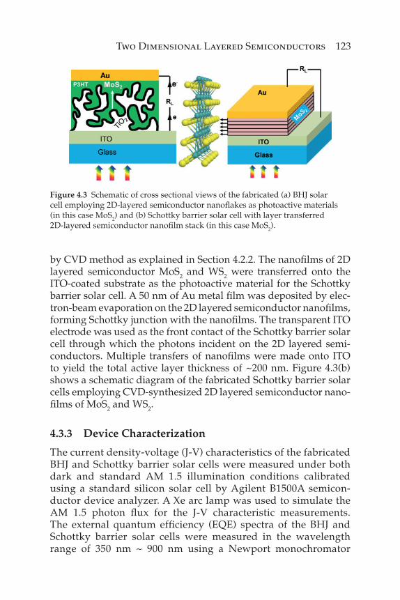
Figure 4.4 shows the scanning electron microscopic (SEM) images of the 2D layered semiconductor nanofl akes (in this case WS2 nanofl akes) coated TiO2 nanoparticle fi lm on glass substrate (a) cross sectional view and (b) surface morphology. The cross- sectional SEM image shows the thicknesses of the 2D layered semiconductor WS2-coated TiO2 was about 12.7 μm as shown. A clear difference between the WS2-coated porous TiO2 fi lms and the glass substrate is observed. Surface morphology of the WS2-coated porous TiO2 fi lm is shown in Figure 4.4(b). It is observed that ran-domly oriented TiO2 nanoparticles with an average size of ~20 nm are well interconnected to each other which facilitate effective electron transport in BHJ solar cells as an electron acceptor. The fi lm is highly porous and clusters of TiO2 nanoparticles are formed as can be seen in the surface morphology. Since the nanofl akes of WS2 obtained by the ultrasonication process are a combination of monolayer and a few layer stacks, it is diffi cult to visualize them separately by SEM.
(a) (b)
30 nm
Figure 4.4 SEM images of 2D-layered semiconductor nanofl akes coated TiO2 electron acceptor used for BHJ solar cell fabrication showing (a) cross sectional view of 12.7 μm thick layer and (b) surface morphology of highly porous TiO2 network coated by 2D-layered semiconductor nanofl akes.
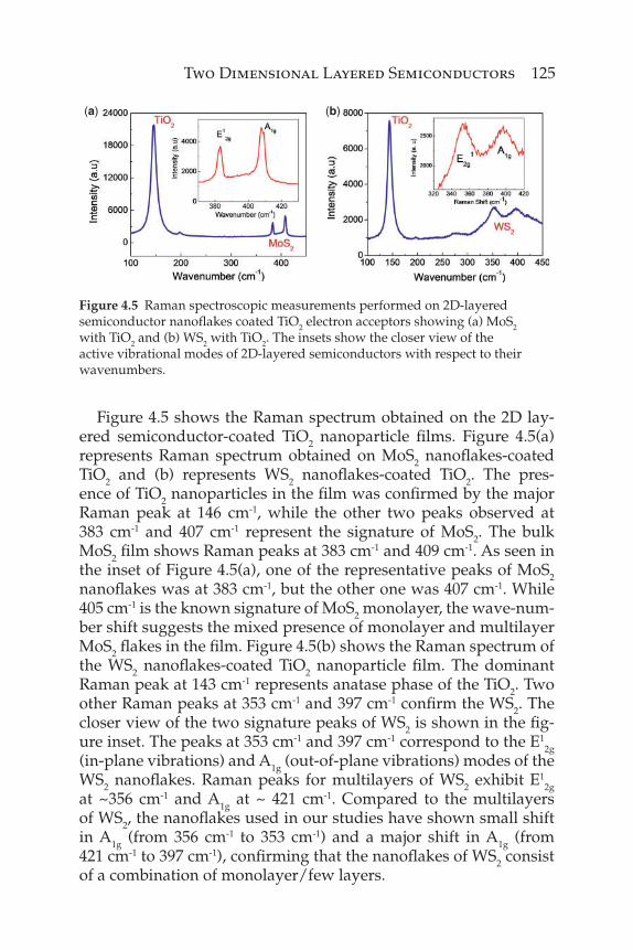
Two Dimensional Layered Semiconductors 125
Figure 4.5 shows the Raman spectrum obtained on the 2D lay-ered semiconductor-coated TiO2 nanoparticle fi lms. Figure 4.5(a) represents Raman spectrum obtained on MoS2 nanofl akes-coated TiO2 and (b) represents WS2 nanofl akes-coated TiO2. The pres-ence of TiO2 nanoparticles in the fi lm was confi rmed by the major Raman peak at 146 cm-1, while the other two peaks observed at 383 cm-1 and 407 cm-1 represent the signature of MoS2. The bulk MoS2 fi lm shows Raman peaks at 383 cm-1 and 409 cm-1. As seen in the inset of Figure 4.5(a), one of the representative peaks of MoS2 nanofl akes was at 383 cm-1, but the other one was 407 cm-1. While 405 cm-1 is the known signature of MoS2 monolayer, the wave-num-ber shift suggests the mixed presence of monolayer and multilayer MoS2 fl akes in the fi lm. Figure 4.5(b) shows the Raman spectrum of the WS2 nanofl akes-coated TiO2 nanoparticle fi lm. The dominant Raman peak at 143 cm-1 represents anatase phase of the TiO2. Two other Raman peaks at 353 cm-1 and 397 cm-1 confi rm the WS2. The closer view of the two signature peaks of WS2 is shown in the fi g-ure inset. The peaks at 353 cm-1 and 397 cm-1 correspond to the E1
2g (in-plane vibrations) and A1g (out-of-plane vibrations) modes of the WS2 nanofl akes. Raman peaks for multilayers of WS2 exhibit E1
2g at ~356 cm-1 and A1g at ~ 421 cm-1. Compared to the multilayers of WS2, the nanofl akes used in our studies have shown small shift in A1g (from 356 cm-1 to 353 cm-1) and a major shift in A1g (from 421 cm-1 to 397 cm-1), confi rming that the nanofl akes of WS2 consist of a combination of monolayer/few layers.
(a) (b)
Figure 4.5 Raman spectroscopic measurements performed on 2D-layered semiconductor nanofl akes coated TiO2 electron acceptors showing (a) MoS2 with TiO2 and (b) WS2 with TiO2. The insets show the closer view of the active vibrational modes of 2D-layered semiconductors with respect to their wavenumbers.
126 Solar Cell Nanotechnology
4.5 Photovoltaic Performance Evaluation
4.5.1 BHJ Solar Cells
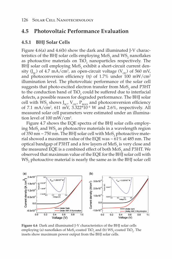
Figure 4.6(a) and 4.6(b) show the dark and illuminated J-V charac-teristics of the BHJ solar cells employing MoS2 and WS2 nanofl akes as photoactive materials on TiO2 nanoparticles respectively. The BHJ solar cell employing MoS2 exhibit a short-circuit current den-sity (JSC) of 4.7 mA/cm2, an open-circuit voltage (VOC) of 560 mV, and photoconversion effi ciency (η) of 1.7% under 100 mW/cm2 illumination level. The photovoltaic performance of the solar cell suggests that photo-excited electron transfer from MoS2 and P3HT to the conduction band of TiO2 could be suffered due to interfacial defects, a possible reason for degraded performance. The BHJ solar cell with WS2 shows JSC, VOC, PMAX and photoconversion effi ciency of 7.1 mA/cm2, 611 mV, 3.322*10–4 W and 2.6%, respectively. All measured solar cell parameters were estimated under an illumina-tion level of 100 mW/cm2.
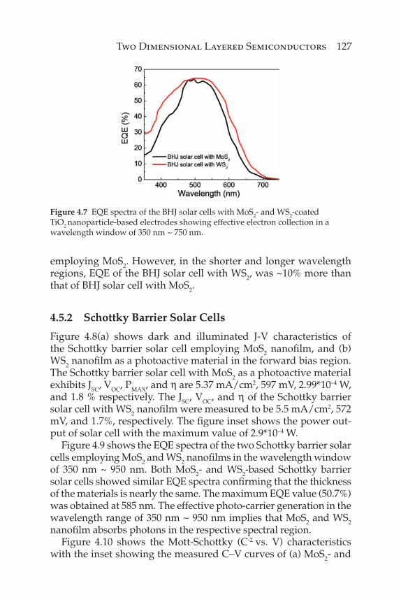
Figure 4.7 shows the EQE spectra of the BHJ solar cells employ-ing MoS2 and WS2 as photoactive materials in a wavelength region of 350 nm ~ 750 nm. The BHJ solar cell with MoS2 photoactive mate-rial showed a maximum value of the EQE was ~ 61% at 485 nm. The optical bandgap of P3HT and a few layers of MoS2 is very close and the measured EQE is a combined effect of both MoS2 and P3HT. We observed that maximum value of the EQE for the BHJ solar cell with WS2 photoactive material is nearly the same as in the BHJ solar cell
(a) (b)
Figure 4.6 Dark and illuminated J-V characteristics of the BHJ solar cells employing (a) nanofl akes of MoS2-coated TiO2 and (b) WS2-coated TiO2. The insets show maximum power output from the BHJ solar cells.
Two Dimensional Layered Semiconductors 127
employing MoS2. However, in the shorter and longer wavelength regions, EQE of the BHJ solar cell with WS2, was ~10% more than that of BHJ solar cell with MoS2.
4.5.2 Schottky Barrier Solar Cells
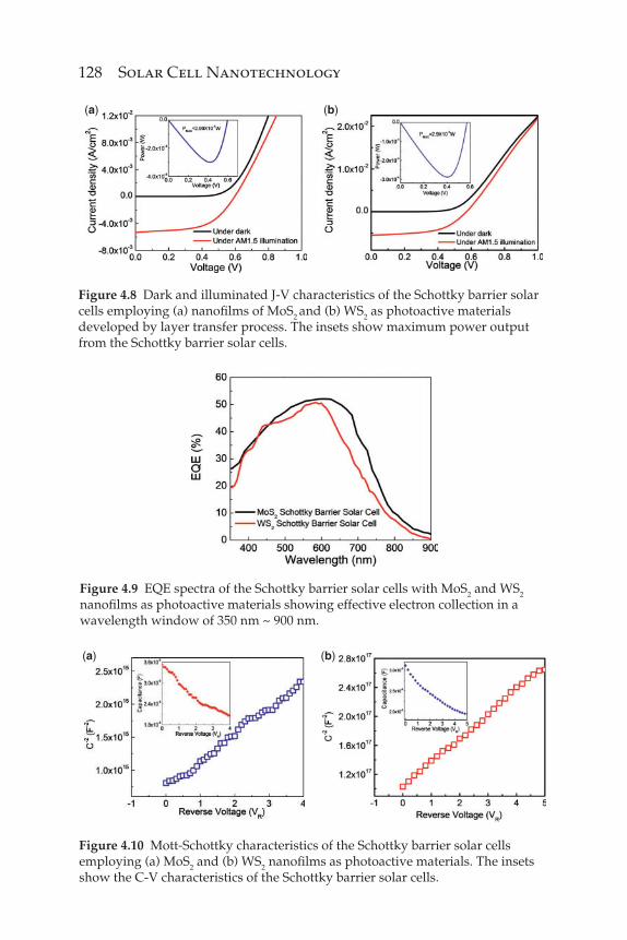
Figure 4.8(a) shows dark and illuminated J-V characteristics of the Schottky barrier solar cell employing MoS2 nanofi lm, and (b) WS2 nanofi lm as a photoactive material in the forward bias region. The Schottky barrier solar cell with MoS2 as a photoactive material exhibits JSC, VOC, PMAX, and η are 5.37 mA/cm2, 597 mV, 2.99*10–4 W, and 1.8 % respectively. The JSC, VOC, and η of the Schottky barrier solar cell with WS2 nanofi lm were measured to be 5.5 mA/cm2, 572 mV, and 1.7%, respectively. The fi gure inset shows the power out-put of solar cell with the maximum value of 2.9*10–4 W.
Figure 4.9 shows the EQE spectra of the two Schottky barrier solar cells employing MoS2 and WS2 nanofi lms in the wavelength window of 350 nm ~ 950 nm. Both MoS2- and WS2-based Schottky barrier solar cells showed similar EQE spectra confi rming that the thickness of the materials is nearly the same. The maximum EQE value (50.7%) was obtained at 585 nm. The effective photo-carrier generation in the wavelength range of 350 nm ~ 950 nm implies that MoS2 and WS2 nanofi lm absorbs photons in the respective spectral region.
Figure 4.10 shows the Mott-Schottky (C-2 vs. V) characteristics with the inset showing the measured C–V curves of (a) MoS2- and
Figure 4.7 EQE spectra of the BHJ solar cells with MoS2- and WS2-coated TiO2 nanoparticle-based electrodes showing effective electron collection in a wavelength window of 350 nm ~ 750 nm.
128 Solar Cell Nanotechnology
(a) (b)
Figure 4.8 Dark and illuminated J-V characteristics of the Schottky barrier solar cells employing (a) nanofi lms of MoS2 and (b) WS2 as photoactive materials developed by layer transfer process. The insets show maximum power output from the Schottky barrier solar cells.
Figure 4.9 EQE spectra of the Schottky barrier solar cells with MoS2 and WS2 nanofi lms as photoactive materials showing effective electron collection in a wavelength window of 350 nm ~ 900 nm.
(a) (b)
Figure 4.10 Mott-Schottky characteristics of the Schottky barrier solar cells
employing (a) MoS2 and (b) WS
2 nanofi lms as photoactive materials. The insets
show the C-V characteristics of the Schottky barrier solar cells.
Two Dimensional Layered Semiconductors 129
(b) WS2-based Schottky barrier solar cells. Linear dependency of C-2 on V behavior was observed in the reverse voltage bias region con-fi rming that the CVD-grown MoS2 and WS2 nanofi lms are n-type doped. The C-V characteristic of the Schottky barrier solar cell is given by Eq. 4.1,
( )2 2
21 R bi
s D
V V
C q N Ae+
=
(4.1)
where VR is reverse voltage bias, Vbi is built-in-potential, q is elec-tronic charge, εs is permittivity, ND is doping density in the MoS2 and WS2 nanofi lms, and A is the junction area. The value of Schottky barrier height was acquired by extrapolating the linear C-2 region to the abscissa, yielding about ~0.5 eV in both MoS2- and WS2-based Schottky barrier solar cells. Under forward applied bias, Fermi levels of 2D layered semiconductors and Au metal contact shift upward and downward, respectively, with respect to the value at equilibrium condition (zero applied bias). Under reverse applied bias, Fermi levels shift in the opposite direction, forming maximum Schottky barrier height. The layer-structured MoS2 and WS2 nano-fi lms possess dangling-bond-free surface on which the recombina-tion velocity of photogenerated carriers would be much lower than that of conventional semiconductors. However, since each MoS2 and WS2 nanofi lm in the active layer stack of the Schottky barrier solar cell was manually transferred, we expect that microstructural deformation might have been introduced into the stack. This could be a major factor that deteriorates the Schottky barrier height in both solar cells.
4.6 Electronic Transport and Interfacial Recombination
4.6.1 BHJ Solar Cells
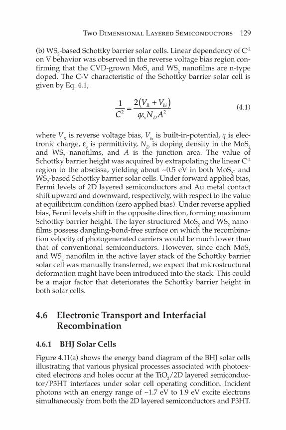
Figure 4.11(a) shows the energy band diagram of the BHJ solar cells illustrating that various physical processes associated with photoex-cited electrons and holes occur at the TiO2/2D layered semiconduc-tor/P3HT interfaces under solar cell operating condition. Incident photons with an energy range of ~1.7 eV to 1.9 eV excite electrons simultaneously from both the 2D layered semiconductors and P3HT.
130 Solar Cell Nanotechnology
The photogenerated electrons are injected into the conduction band of the TiO2 in which electrons diffuse to reach the ITO electrode. Processes (1) and (2) in Figure 4.11(a) represent electron injection from the lowest unoccupied molecular orbital (LUMO) of P3HT to the con-duction band of 2D layered semiconductor (in this case MoS2). Process (3) represents hole transport from the valence band of the MoS2 to the highest occupied molecular orbital (HOMO) of the P3HT and then to the Au back contact. These three processes (1 to 3) are favorable to enhance the solar cell performance. However, due to the large surface area of TiO2, surface states (recombination centers) exist in the band-gap of TiO2 in which photoinjected electrons can be trapped from the conduction band and recombine with holes present at the valence band of MoS2. Process (4) represents electron capture by TiO2 surface state followed by hole capture (process (5)) from the valence band of
(b)
(a)
Figure 4.11 Energy level alignment in the (a) BHJ solar cells showing major electron transport and recombination processes occuring at TiO2/2D-layered semiconductor/P3HT interfaces (b) Schottky barrier solar cell with ITO/2D-layered semiconductor/metal interfaces.
Two Dimensional Layered Semiconductors 131
MoS2-coated on TiO2. We propose that it is these two interfacial pro-cesses (electron and hole capture) which eventually lead to recombi-nation and deteriorate the solar cell performance signifi cantly.
The Shockley-Read-Hall (SRH) recombination model [37] can explain the major interfacial recombination processes and gives electron lifetime (Eq. 4.2),
( ) ( )0 1 0 1
0 0
p n n p
SRHn
n n p p
p n
t tt
+ + Δ + + + Δ=
+ + Δ
(4.2)
where τp and τn are lifetimes of hole and electron, respectively. The n0 and p0 are electron and hole densities at thermal equilibrium con-dition (no excess electron-hole pair generation). The Δn and Δp are the excess electrons and holes generated by the BHJ solar cell under illumination condition. Further, the electron and hole lifetimes can be defi ned by 1
nn Th TV N
ts
= and 1p
p Th TV Nt
s= where σn and σp are cap-
ture cross-sections for electrons and holes, respectively. The quanti-ties VTh and NT represent thermal velocity and density of TiO2 surface states often called as trap states. As the density of TiO2 surface states increases in the large surface area TiO2 nanoparticle layer, electron lifetime decreases signifi cantly due to an increase in the probability of recombination via TiO2 surface states. In Eq. 4.2 the quantities n1 and p1 are electrons and holes that participate in the transport and recombination process at TiO2/2D layered semiconductors interfaces under illumination condition. The electrons and holes take part in the transport process caused by the presence of TiO2 surface states that are distributed all over the bandgap. However, only those sur-face states close to valence band of the 2D layered semiconductors would actively participate in the capture and recombination process due to the presence of free holes at valence band. The same analysis for electronic transport and recombination processes is valid in the case of BHJ solar cell with WS2 as a photoactive material candidate. Both MoS2 and WS2 behave very similarly in photonic absorption as they possess very similar optical bandgap values.
4.6.2 Schottky Barrier Solar Cells
Figure 4.11(b) shows the energy band diagram of the fabricated Schottky barrier solar cells having a stacked structure of ITO/2D
132 Solar Cell Nanotechnology
layered semiconductors/Au. If the metal work function is higher than that of n-type semiconductor, then an ideal Schottky barrier could be formed. Au metal fi lm with a work function: ~5.1 eV forms a Schottky barrier on 2D layered semiconductors MoS2 and WS2 (work function: ~4.6 eV). Work function of ITO is ~4.5 eV which is suitable to form a good Ohmic contact with n-type doped MoS2 and WS2 nanofi lms. Since the ITO is heavily doped material, its Fermi level enters into the conduction band as shown in Figure 4.11(b). Optical bandgap of the 2D layered semiconductors changes from monolayer to six layers (in the case of MoS2) and becomes constant. Therefore layer dependency of optical bandgap becomes negligible while bulk material is employed in the solar cells. The MoS2- and WS2-stacked nanofi lms used for Schottky barrier solar cells with an optical bandgap of ~1.3 eV effectively absorb photons in the wavelength region of 350 nm ~ 950 nm. ITO does not absorb solar photons in visible spectral window due to the wide bandgap through which the solar cells were illuminated. Incident photons generate electron-hole pairs in the 2D layered semiconductors, and electrons are subsequently excited to the conduction band of 2D layered semiconductors. As the work function difference between Au metal contact and n-type 2D layered semiconductors results in a Schottky barrier, the photoexcited electrons move from the conduc-tion band of 2D layered semiconductors towards the Fermi level of ITO where they can be collected to the external load. A larger work function difference between Au and n-type 2D layered semicon-ductors would generate higher electric fi eld in the depletion region. The photogenerated electron-hole pairs are separated and driven by the built-in electric fi eld developed at the 2D layered semicon-ductor/Au interface. The processes of optical excitation in the 2D layered semiconductor (in this case MoS2) and electron transport from MoS2 to ITO electrode are illustrated in Figure 4.11(b). The same analysis and band energy level alignment can be generalized to the Schottky barrier solar cell employing WS2 as active semicon-ductor material candidate.
4.7 Conclusion and Outlook
While electronic transport in conventional bulk and thin-fi lm semiconductors-based solar cells is limited by electroni-cally active interfacial defects, 2D layered semiconductors offer

Two Dimensional Layered Semiconductors 133
self-terminated, dangling, bond-free surfaces to form interfaces with other active layers in solar cells to achieve effective electronic transport with better control on interfacial recombination. Large area 2D layered semiconductor material development is viable by the CVD method and hence useful for large area solar cell applica-tions. Thickness-dependent physical properties are attractive for photovoltaic technology through which material parameters can be tuned in a simple way. The demonstrated BHJ and Schottky barrier solar cells elucidated 2D layered semiconductors can be considered as potential material candidates for emerging photo-voltaic technology.
References
1. Y. Li, C.-Wei Wang, Y. Zhao, J. Wang, F. Zhou, Journal of Solid State Chemistry, Vol. 196, P. 349, 2012.
2. S. Lu, L. Zeng, T. Wu, B. Ren, J. Niu, H. Liu, X. Zhao, J. Mao, Solar Energy, Vol. 85, p,1967, 2011.
3. M. Wang, X. Wang, Solar Energy Materials and Solar Cells, Vol. 91, p.178223, 2007.
4. J. A. Mikroyannidis, M. M. Stylianakis, P. Suresh, G.D. Sharma, Solar Energy Materials and Solar Cells, Vol. 93, p. 1792,2009.
5. Y. Wang, W. Wei, X. Liu, Y. Gu, Solar Energy Materials and Solar Cells, Vol.98, p. 129, 2012.
6. J. Lee, J. Y. Jho, Solar Energy Materials and Solar Cells, Vol. 95, p. 3152, 2011. 7. J. Bouclé, S. Chyla, M. S.P. Shaffer, J. R. Durrant, D. D.C. Bradley, J. Nelson,
Comptes Rendus Physique, Vol.9, p.110, 2008. 8. Z.J. Wang, S.C. Qu, X.B. Zeng, J.P. Liu, C.S. Zhang, F.R. Tan, L. Jin, Z.G. Wang,
Applied Surface Science, Vol. 255, p.1916, 2008. 9. Y.Y. Yu, W.C. Chien, Y.H. Ko, Y.C. Chan, S. C. Liao, Current Applied Physics,
Vol.12, p.S7, 2012.10. H. Flügge, M. Pfannmöller, G. Benner, I. Wacker, H. Schmidt, T. Rabe,
R. R. Schröder, W. Kowalsky, Energy Procedia, Vol. 31, p.46, 2012.11. M. Bhushan, Appl. Phys. Lett., Vol. 40, p. 51,1982.12. M. Vanecek, A. Abrahám, O. Štika, J. Stuchlík, J. Koka, phys. stat. sol. (a), Vol.83,
p.617,1984.13. Z. B. Zhou, R. Q. Cui, Q. J. Pang, G. M. Hadi, Z. M. Ding, W. Y. Li, Sol. Energy
Mater. Sol. Cells, Vol. 70, p. 487, 2002. 14. B. Ghosh, M. Das, P. Banerjee, S. Das, Solid State Sci. Vol. 11, p. 461, 2009.15. M. Soylu, F. Yakuphanoglu, Thin Solid Films Vol. 519, p. 1950, 2011.16. J. Wei, Y. Jia, Q. Shu, Z. Gu, K. Wang, D. Zhuang, G. Zhang, Z. Wang, J. Luo,
A. Cao, and D. Wu, Nano Lett., Vol. 7, p. 2317, 2007. 17. C. Xie, P. Lv, B. Nie, J. Jie, X. Zhang, Z. Wang, P. Jiang, Z. Hu, L. Luo, Z. Zhu,
L. Wang, and C. Wu, Appl. Phys. Lett., Vol. 99, p. 133113, 2011.
134 Solar Cell Nanotechnology
18. Y. Ye, Y. Dai, L. Dai, Z. Shi, N. Liu, F. Wang, L. Fu, R. Peng, X. Wen, Z. Chen, Z. Liu, and G, Qin, Appl. Mater. Interfaces, Vol. 2, p. 3406, 2010.
19. L. Zhang, Y. Jia, S. Wang, Z. Li, C. Ji, J. Wei, H. Zhu, K. Wang, D. Wu, E. Shi, Y. Fang,and A. Cao, Nano Lett., Vol. 10, p. 3583, 2010.
20. C. C. Chen, M. Aykol, C. C. Chang, A. F. J. Levi, and S. B. Cronin, Nano Lett., Vol. 11, p. 1863, 2011.
21. P. Broqvist, A. Alkauskas, and A. Pasquarello, Phys. Rev. B, Vol. 78, p. 075203, 2008.
22. R. Brüggemann, G.H Bauer, J. Non-Cryst. Solids, Vol. 227, p.197, 1998.23. E. Kamiyama, K. Sueoka, Appl. Surf. Sci., Vol. 258, p. 5265, 2012.24. C. Boehme, K. Lips, J. Non-Cryst. Solids, Vol. 338, p. 434, 2004.25. R. Barrio, J. J. Gandía, J. Cárabe, N. González, I. Torres, D. Muñoz, C. Voz, Sol.
Energy Mater. Sol. Cells, Vol. 94, p. 282, 2010.26. P. Repo, H. Talvitie, S.Li, J. Skarp, H. Savin, Energy Procedia, Vol. 8, p. 681, 2011.27. A. Splendiani, L. Sun, Y. Zhang, T. Li, J. Kim, C. Y. Chim, G. Galli, and F. Wang,
Nano Lett., Vol. 10 (4), p. 1271, 2010.28. K. K. Liu, W. Zhang, Y. H. Lee, Y. C. Lin, M. T. Chang, C. Y. Su, C. S. Chang,
H. Li, Y. Shi, H. Zhang, C. S. Lai, and L. J. Li, Nano Lett., Vol. 12 (3), p.1538, 2012.
29. K. F. Mak, C. Lee, J. Hone, J. Shan, T. F. Heinz, Phys. Rev. Lett., Vol. 105, p. 136805, 2010.
30. S. Najmaei, Z. Liu, P. M. Ajayan, and J. Lou, Appl. Phys. Lett. Vol.100, p.013106, 2010.
31. B. Radisavljevic, A. Radenovic, J. Brivio, V. Giacometti, and A. Kis, Nature Nanotechnol. Vol. 6, p.147, 2011.
32. Y. Yoon, K .Ganapathi, and S. Salahuddin, Nano Lett. Vol. 11, p.3768, 2011.33. Y. Zhang, J. Ye, Y. Matsuhashi, and Y. Iwasa, Nano Lett. Vol. 12, p. 1136, 2012.34. H. Qiu, L. Pan, Z. Yao, J. Li, Y. Shi, and X. Wang, Appl. Phys. Lett. Vol. 100,
123104, 2012.35. H. Hwang, H. Kim, and J. Cho, Nano Lett. Vol. 11, p. 4826, 2011.36. M. Shanmugam, T. Bansal, C. A. Durcan, B. Yu, Appl. Phys. Lett. Vol. 100,
p. 153901, 2012.37. W. Shockley, W.T. Read, Phys. Rev., Vol. 87, p. 835, 1952.