solar cells - engineering school class web sites · cell is the spectrum of the solar energy...
TRANSCRIPT
SOLAR CELLS A. PREPARATION
1. History of Silicon Solar Cells
2. Parameters of Solar Radiation
3. Solid State Principles
i Band Theory of Solids
ii. Optical Characteristics
4. Silicon Solar Cell Characteristics
5. Theoretical and Practical Efficiencies
6. Effects of Temperature and Internal Resistances on Cell Efficiency
7. Practical Realizations
i. Applications
ii. Concentrators
iii. Lifetime and Maintenance
8. Cost and Future Prospects
9. References B. EXPERIMENT
1. Equipment List
2. Preliminary Set-up and Calibration
3. Incident IR Energy
3. Photovoltaic VI Characteristics
4. Temperature Effects on Cell Characteristics
5. Solar Cell Sensitivity
6. Temperature Effects on Solar Cells
7. Report
Solar Cells -- I
A. PREPARATION
1. History of Silicon Solar Cells
In 1839, French physicist Alexandre Edmond Becquerel discovered that when light shone on one
of a pair of metal plates immersed in a dilute acid solution, the amount of electric energy moving
through the circuit increased. This was the first glimpse of the "Photoelectric Effect," the ability of
light to generate a flow of electricity. Becquerel's discovery, however, elicited no practical application
until 1954, when after considerable theoretical and experimental work from the date 1930's through the
1940's, researchers at the Bell Telephone Laboratories in New Jersey produced the first practical solar
cell, a planar junction single crystal silicon cell.
The early cells produced soon after were usually circular in shape with a diameter of
approximately 3 cm. They were of the p- or n-, wrap-around contact type with a high internal
resistance (5-10 ohms) and excessive material defects thereby resulting in a relatively low conversion
efficiency (less than 6%). Since the costs of producing these cells was approximately $2000/watt of
power, they were far too expensive for any use known to man until the advent of the space program. In
1958, Vanguard, the first U.S. satellite, went into space carrying six rectangular 0.5 x 2 cm cells. Not
realizing the implications of the long life of the silicon cells, Vanguard continued to send radio signals
back to Earth for 6 years due to the omission of an "off" switch by scientists.
Although the space program provided the incentive to develop more efficient solar cells, it was
not until 1972 that a 30% increase in energy conversion efficiency was obtained for space application
cells. This was achieved by decreasing the internal resistance of the cell to about 0.05 ohms, improving
the charge carrier collection process, and increasing the cells "blue" response. The resulting solar cell
was best known as the
Solar Cells-- 2

"Violet" cell.
Another noteworthy development in 1972 was the Vertical Multijunction (VMJ) solar cell,
also known as the edge-illuminated multijunction cell. This device was unusual in that it was
constructed by stacking alternate layers of n- and p-type silicon into a stack very similar to that
of a "layer cake." This stack then stood vertical with the illumination entering on the sides of the
layers. A pair of ohmic contacts on each end of the stack allowed for the extraction of usable
power. The characteristics of this device included a low internal resistance coupled with a high
device voltage at a very low current.
From 1972 to 1976, a variety of cells were designed for space applications while research
on terrestial solar cell uses continued to crag due to the high commercial production costs of
silicon cells. These new designs were developed by improving on such cell characteristics as
solar energy spectrum sensitivities (resulting in "ultra-blue,""blue-shifted", and "superblue"
cells), carrier collection processes ("drift-field" and "p+ " cells), and light reflection processes
on the cells exposed surfaces ("non-reflecting", "black", and "textured" cells). Perhaps the most
notable improvement in space application solar cells during this time period was the
development of the ultra-thin single crystal silicon solar cell. These 0.05 mm cells were tested
in 1978 and were found to exhibit efficiencies that reached 12.5% as well as having a high
radiation resistance (important for space applications), and a low weight.
Toward the end of the 1970's, it became obvious that in order to make silicon solar cells
feasible for terrestrial applications, high efficiency cells would have to be made available at a
much lower cost. However, since efficiencies were already in the 10-13% range, the major
emphasis was placed on lowering the cell fabrication costs instead of on improving the
efficiencies.
Solar Cells--3

This effort was rewarded when it became possible to grow larger, purer, and more stress-free
silicon crystals employing new cutting techniques that reduced work damage suffered by the
silicon. Due to this major improvement as well as other smaller advances, what once cost
$2000 per watt now only cost about $8 per watt. Although this is still too expensive for most
terrestial applications, with all the research being performed today on solar energy converters,
as well as on other materials such as GaAs, CdS, CdTe, and InP, it is worthwhile to note that
while the cost of most electricity generating processes continues to rise, the cost of solar energy
keeps falling. Therefore, it is not unreasonable to assume that one day, solar cells may be
producing a substantial portion of our electrical needs.
2. Parameters of Solar Radiation
The maximum usable power that can be delivered to a load by a solar cell is Proportional
to the amount of solar energy incident upon the cell. Therefore, it is obvious that the output
can be seriously affected by changes in both climatic and weather conditions. In addition, the
cell output will also be determined by such solar intensity variations as those that occur
seasonally, diurnally, and with geographical location as well as the spectral content of the
solar illumination itself.
The total energy received from the sun on a unit area perpendicular to the sun's rays at
the mean earth-sun distance (1.496 x 10¹¹m = 1.00 Astronomical Unit = 1.00 AU) is called the
Solar Constant. Originally thought to be 140.0 mW/cm2, it was revised in 1971 to the present
value of 135.3 mW/cm2. Because the solar constant refers to the total radiant energy received
at 1 AU, when referring to the total radiant energy received at a given distance other than 1
AU, it is best to use the term "solar irradiance" (sometimes called the solar intensity, a term
that will appear throughout
Solar Cells -- 4

the remainder of this report) .
Throughout the year, the distance between the earth and the sun
varies due to the fact that the earth revolves around the sun in a
slightly elliptic path. This variation in the earth-sun distance in
turn gives rise to annual deviations in the solar intensity falling
on the earth's surface. Presented in Table 1 are values of the total
solar intensity as a function of the earth-sun distance. Note that
the peak values occur ding the winter months of December, January,
and February.
DATE SOLAR INTENSITY
(mW per cm2)
January 3 139.9
February 1 139.3
March 1 137.8
April 1 135.5
May 1 133.2
June 1 131.6
July 4 130.9
August 1 131.3
September 1 132.9
October 1 135.0
November 1 137.4
December 1 139.2
Table 1
In addition to the seasonal variations, the amount of sunlight
falling on a specific geographic location, known as the solar
insolence, is dependent upon such factors as the locations latitude,
the prevailing local climate, and even the local air pollution
levels. Shown in Figure 1 are the seasonal variations in incident
solar energy for two major U.S. cities geographically separated by a
large distance, Alburquerque, N.M. (Lat. 35.05 N), and Cleveland, OH
(Lat. 41.40 N). These measurements were both taken utilizing an
aperture in a plane surface tilted down from a horizontal position
toward the South by an angle equal to the local latitude and fixed in
position, thus allowing readings of both diffuse sky and direct solar
radiation, but
Solar Cells -- 5
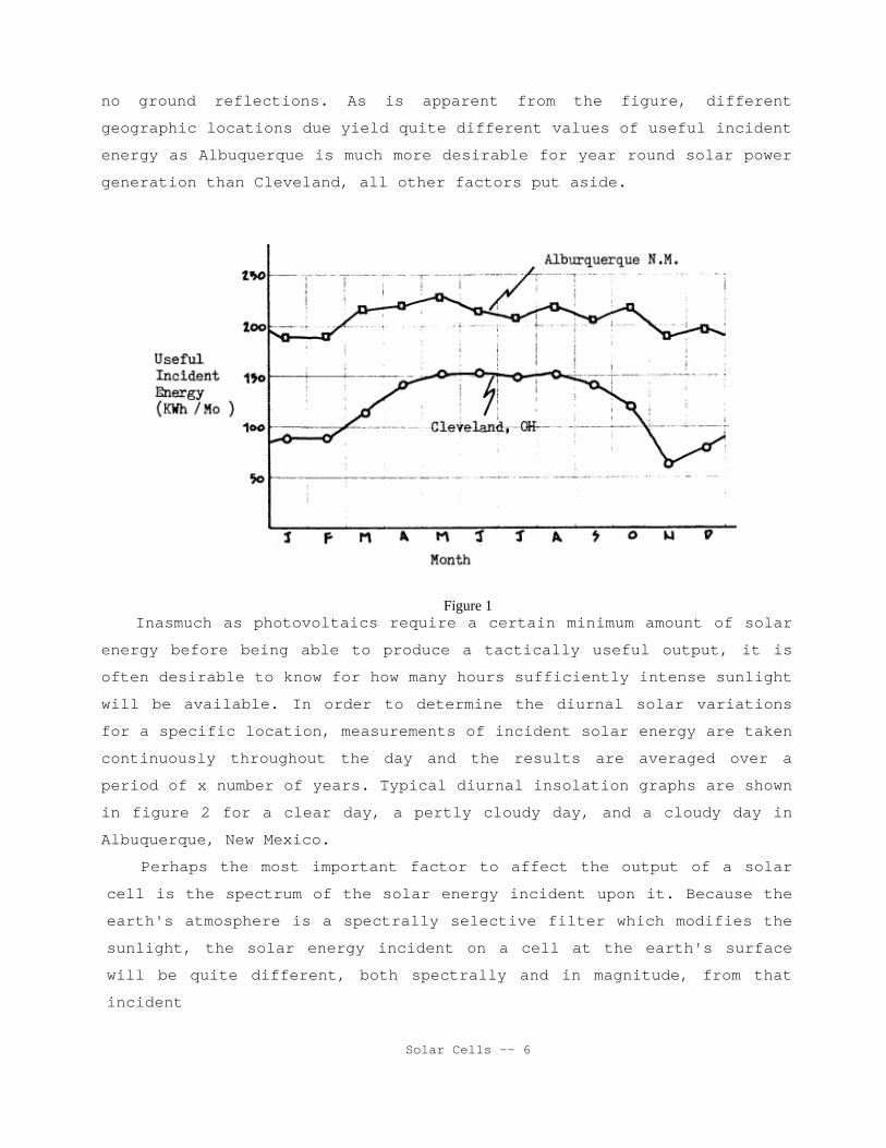
no ground reflections. As is apparent from the figure, different
geographic locations due yield quite different values of useful incident
energy as Albuquerque is much more desirable for year round solar power
generation than Cleveland, all other factors put aside.
Figure 1 Inasmuch as photovoltaics require a certain minimum amount of solar
energy before being able to produce a tactically useful output, it is
often desirable to know for how many hours sufficiently intense sunlight
will be available. In order to determine the diurnal solar variations
for a specific location, measurements of incident solar energy are taken
continuously throughout the day and the results are averaged over a
period of x number of years. Typical diurnal insolation graphs are shown
in figure 2 for a clear day, a pertly cloudy day, and a cloudy day in
Albuquerque, New Mexico.
Perhaps the most important factor to affect the output of a solar
cell is the spectrum of the solar energy incident upon it. Because the
earth's atmosphere is a spectrally selective filter which modifies the
sunlight, the solar energy incident on a cell at the earth's surface
will be quite different, both spectrally and in magnitude, from that
incident
Solar Cells -- 6
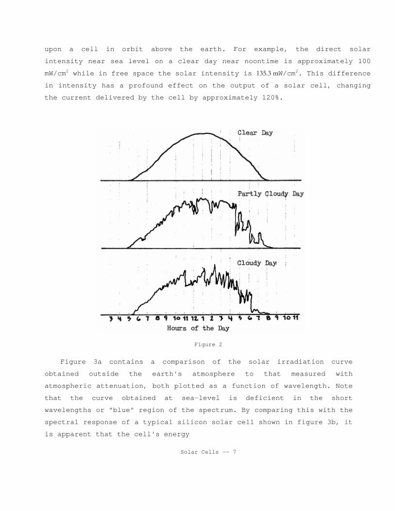
upon a cell in orbit above the earth. For example, the direct solar
intensity near sea level on a clear day near noontime is approximately 100
mW/cm2 while in free space the solar intensity is 135.3 mW/cm2. This difference
in intensity has a profound effect on the output of a solar cell, changing
the current delivered by the cell by approximately 120%.
Figure 2
Figure 3a contains a comparison of the solar irradiation curve
obtained outside the earth's atmosphere to that measured with
atmospheric attenuation, both plotted as a function of wavelength. Note
that the curve obtained at sea-level is deficient in the short
wavelengths or "blue" region of the spectrum. By comparing this with the
spectral response of a typical silicon solar cell shown in figure 3b, it
is apparent that the cell's energy
Solar Cells -- 7

conversion efficiency will be higher for sea-level spectral conditions than for free space conditions. The
reason is that, because of the deficiency in the shorter wavelengths, a relatively greater percentage of the
total incident solar energy is then in the larger wavelength region of the spectrum, a region where the cell
is spectrally more sensitive. Therefore, in the design of photovoltaics for either space or terrestial
applications, the spectral response of the cell should be designed such that it is more sensitive to the solar
spectrum available in the environment in which it will be utilized.
Figure 3
3, Solid State Principles
Solid materials can be basically categorized into three major
groups: insulators, conductors, and semiconductors. When considering
the conductivities of solid materials, we note that the range of
values from conductive materials to materials considered insulators is
quite enormous. Representative values are from 6 x 10? S /m for silver,
a good conductor, to less than 2 x 10-17 S /m for fused quartz, a good
insulator. However, it is the
Solar Cells -- 8

materials with the intermediate conductivity values, the
semiconductors, which we are most interested in. The basic reason is
that all of the practical solar cells developed to date are made with
semiconductors. Therefore, this report continues with a discussion on
the basic principles of semiconductor materials.
i. Band Theory of Solids
When isolated atoms are brought together to form a solid, various
interactions occur between the neighboring atoms, particularly those
arising from the bonding activities of these atoms and their electrons.
In the process, important changes occur in. the electron energy level
configurations which result in the varied electrical properties of
different solids.
If anything, from freshman chemistry, you should recall that
electrons in isolated atoms can exist only at discrete or quantized
energy levels. Furthermore, it is known that the Pauli exclusion
principle limits the number of electrons that can exist at any of the
allowed energy levels. As atoms are brought closer together, as in a
crystal, so that their electron wave functions begin to overlap, the
exclusion principle dictates that no two electrons in a given
interacting system may have the same quantum state, therefore, the
discrete energy levels of the isolated atoms must split into new levels
belonging to the pair rather than the individual atoms. Because of the
large number of atoms brought together in a solid (crystal); there may
be 1022 atoms in a crystal, the split energy levels will essentially
form continuous bands of energies. These electron energy levels in the
material can be represented by the energy diagrams shown in figure 4,
depicting both the allowed energy levels and the ranges of energies in
between the allowed bands where electrons are forbidden to exist. This
gap is oftentimes referred to as the "forbidden band" since in a perfect
crystal it contains no electron energy states. Because every solid has
its own characteristic energy band structure,
Solar Cells --9

Figure 4
it is the variations in the band structure and the distribution of
electrons in the outermost or highest energy bands which are responsible
for the wide range of electrical characteristics observed in various
materials.
In order to understand why a solid is a good conductor or a good
insulator, it is necessary to study the fundamentals of electron
movement within the solid, in other words, the mechanisms of current
flow. The number of electrons in a solid is usually a small percentage
of the total allowed energy locations available with the electrons
constantly seeking lower energy levels. However, due to either thermal
or optical excitation, the electrons are constantly being excited to
higher energy states. The distribution of the electrons in the allowed
levels can be described by the
Fermi function:
1]/)exp[(1)(
+−=
kTEEEF
f
where E is the energy of the allowed state, Ef is the Fermi energy, k is
Boltzmann's constant, and T is the absolute temperature. Of particular
interest is the Fermi energy (also called the Fermi level), Ef, defined
as the energy at which the probability of a state being filled is
approximately 1/2; or in other words, the highest energy state an
electron can have at 0ºK. The Fermi level is a very important concept
and plays an enormous

Solar Cells -- 10

role in electron movement.
In order for electrons to experience acceleration from either
thermal or optical excitation, they must be able to move into new
energy states. This implies that there must be allowed energy states
not yet occupied by electrons (empty states) available to the excited
electrons. Returning to figure 4, the highest occupied band in this
diagram corresponds to the ground state of the outermost or valence
electrons of the atom, the electrons responsible far current flow.
Therefore, as one would expect, this band is cal-led the valence band
while the upper band is termed the conduction band and the distance
between these bands is defined as the energy gap, Eg. As is apparent
from figure 4a, b, insulators are very similar to semiconductors at
0°K. For both types of materials the valence bend is full and the
conduction band is empty. As a result, there can be no charge
transport in the conduction band since there are no electrons present
and because there are no empty states available in the valence band
into which electrons can move, no charge transport can occur here
either. However, there is a difference between the insulator and the
semiconductor which accounts for their dissimilarity in conductivity.
This is due to the fact that the band gap fox insulating materials is
much larger than that for semiconductors. For example, silicon, a
semiconductor, has a band gap of 1.1 eV as compared to 10 eV for
Alumina (A1203). The relatively small band gap for semiconductors thus
allows for excitation of electrons from the valence band to the
conduction band by reasonable quantities of thermal or optical energy.
Therefore, at room temperature, a semiconductor with a 1.1 eV band gap
will have a significant number of electrons excited across the energy
gap into the conduction band whereas an insulator with a 10 eV energy
gap will have a negligible number of electron excitations.
Finally, in figure 4c is the band gap diagram for a metal in which
the
Solar Cells -- 11

bands either overlap or are only partially filled. Thus electrons and
empty energy states are intermixed within the bands so that electrons
can move freely under the influence of any type of excitation. This
accounts for the fact that metals have a high electrical conductivity.
The type of semiconductor discussed above is an intrinsic
semiconductor in which the conduction of current is due only to those
electrons excited up from the valence band to the conduction band.
This material is usually produced with ultra-high purity materials and
by slowly growing large single gain crystals, very low defect
semiconductors can be made. However, by adding small amounts of
impurities called dopants at carefully controlled levels to the
semiconductor crystals, it is possible to dictate the dominant type of
conduction; either electrons or holes*. This type of material is
called an extrinsic semiconductor because the conduction is due to the
impurities added. Consider figure 5a., which shows the two dimensional
diamond structure of a pure silicon crystal with its normal covalent
bonds that exist by the sharing of electrons. This is an intrinsic
semiconductor and its band structure is shown below it (note the Fermi
level is roughly in the center of the energy gap). In figure 5b, one
of the silicon atoms has been replaced by doping with a phosphorus
atom which supplies an extra electron. Since this extra electron is
held in place only by the coulomb attraction to the phosphorus
nucleus, it can be removed and excited to the conduction band with
much less energy than is required to move a valence electron across
the band gap. On the corresponding band diagram, this has the effect
of shifting the Fermi level toward the conduction band plus providing
a donor level that donates extra electrons to the conduction band
thereby making the electrons
"holes" are empty states in the valence band into which electrons can
move; current can also be pictured as positively charged holes
moving in the opposite direction of electrons.
Solar Cells --12

the majority charge carriers. This is an example of an "n-type"
extrinsic semiconductor.
Figure 5
Figure 5c contains an example when the material is doped by
aluminum, which has a deficiency of one electron thereby contributing
an extra hole to the lattice structure. This allows far a valence
electron to jump into this hole with far less energy than that required
to excite it across the energy gap, thus creating another hole in its
vacated spot and the result is positive charge conduction. The addition
of these extra holes into the crystal lattice thus provides an acceptor
energy level, Ea, in the band gap which accepts electrons from the
valence band easily. Therefore, in this case, the holes are the
majority charge carrier and the resulting material is an example of a
"p-type" extrinsic semiconductor.
ii. Optical Characteristics
By definition, the photovoltaic effect is the generation of a
potential when radiation (photons) ionizes the region in or near the
built-in potentia1
Solar Cells --13

barrier of a semiconductor. However, in order to obtain useful power
from the photon interactions in the material, three essential processes
must occur:
1. A photon has to be absorbed and result in electrons being
excited to a higher potential.
2. The electron-hole charge carriers created by the absorption must
be separated and moved to the edge to be collected.
3. The charge carriers must be removed to a useful load before they
recombine with each other and lose their added potential energy.
For an incoming photon to be completely absorbed by an electron, it
must possess an energy greater than the forbidden band energy, Eg,
thereby allowing the electron to jump the gap into the conduction band.
Any excess energy above the minimum energy required is usually given up
to the lattice as thermal energy. If, however, the photon has an energy
less than Eg, the material will essentially appear transparent as there
is no mechanism with which the electron could interact.
Once the photons have been absorbed and the electron-hole pairs
(EHP's) generated, the charges must then be separated. This is typically
accomplished by means of a potential barrier formed when a p-type
material is brought into contact with an n-type material thus creating a
p-n junction semiconductor." The energy level diagram for a typical p-n
silicon solar cell is shown in figure 6.
Figure 6
Solar Cells -- 14
Notice the Fermi level of the n-type material is near the top of the energy gap
and thus there are many electrons in the conduction band and only a few holes
in the valence band. However, for the p-type material, the opposite is true.
This leads to the concept of minority and majority carriers. Since at a given
temperature the product of the number of holes and the number of electrons is
essentially constant (1021 for silicon @ 27ºC), for n-type silicon, n could be
1017/cm3 while p is 104/cm3. When a solar cell (p-n junction) is exposed to
light, all incident photons with energy greater than Eg create an EHP. For a
very intense light source where a large number of EHP's are generated, the
result is that the minority carrier concentration will increase many orders of
magnitude while the majority carrier concentration will essentially remain the
same. Therefore, an excess of minority carriers will occur and they will
diffuse throughout the material until recombination occurs, usually within a
few tenths of a microsecond.
However, if the excess carriers are generated within a diffusion length*
of the p-n potential barrier, the electric field induced by the junction will
sweep the excess carriers across the junction in an attempt to reduce their
energy. As depicted in figure 6, the excess electrons will flow to the left and
the excess holes to the right. This creates an electric current moving from
the p-type to the n-type material which can be funneled to deliver power to a
load if the proper connections are made as in figure 7. The current generated
will be proportional to the number of photons absorbed and the voltage
produced will depend on the height of the barrier which in turn depends on how
heavily the n and p regions are doped.
* The diffusion length is the average distance a carrier diffuses before
recombination.
** A typical silicon solar cell (like the one used in this experiment) is
:jade by first slicing a .015 inch thin wafer from an ingot of silicon
that contains traces of boron, which makes the wafer receptive to
electrons. Then it is heated to remove stresses and put into a furnace
containing phosphorus vapor. The phosphorus then works its way into both
sides c= the wafer, forming a thin layer of n-type silicon. One of these
sides is chemically removed and the wafer is
Solar Cells -15

Figure 7
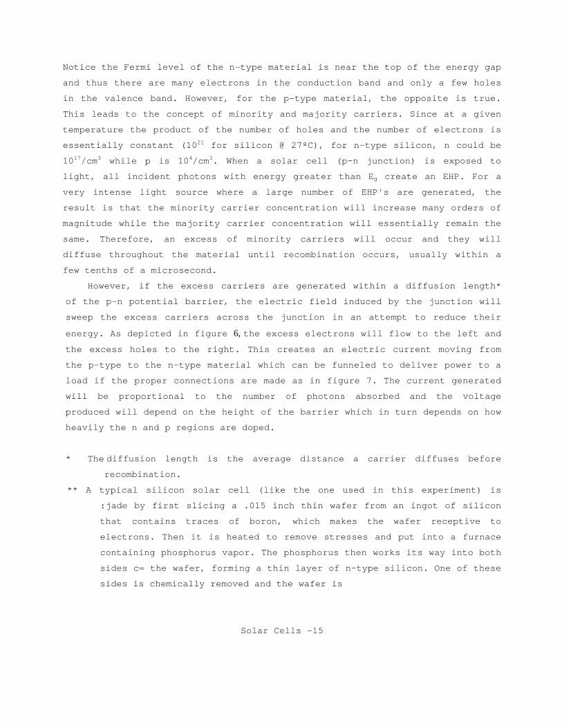
4. Silicon Solar Cell Characteristics
The silicon Solar cell used in this experiment can essentially be
represented by the simplified equivalent circuit shown in figure 8, which
consists of a constant current generator in parallel with a nonlinear junction
impedance (Zj) and a resistive load (Rl). When light strikes the cell, a
current Is (short-circuit current) is generated which is equal to the sum of
the current through the load, IL, and the current flowing in the nonlinear
junction, Ij.
Therefore: jIIIWith
where q is the electron charge, V is the applied junction voltage, k is the
Boltzmann constant, T is the absolute temperature, and Io is the dark (reverse)
saturation current. Hence, the current through the load is given
by: (03) )1( /0 −−= kTqV
sL eIII
and the maximum voltage obtained from the cell, Vmax; occuring when IL=0,
is:
where kTq /=λ
Shown in figure 9 is a general solar cell VI characteristic with both Io
and Is Plotted. Note that the curves appear in the fourth quadrant, there
Solar Cells--16
(01) Ls +=(02) )1/(0 −= kTeI qV
/(04) )1)/ln(()//(1
0
0max
=
I j
(05) )1)/ln((1 +=
IIIkTqV
s
s
Iλ+
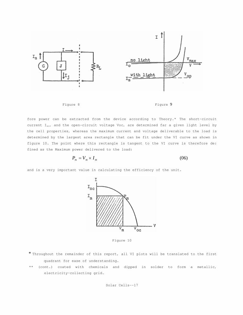
Figure 8 Figure 9
fore power can be extracted from the device according to Theory.* The short-circuit
current Isc, and the open-circuit voltage Voc, are determined far a given light level by
the cell properties, whereas the maximum current and voltage deliverable to the load is
determined by the largest area rectangle that can be fit under the VI curve as shown in
figure 10. The point where this rectangle is tangent to the VI curve is therefore de:
fined as the Maximum power delivered to the load:
(06) mmm IVP ×=
and is a very important value in calculating the efficiency of the unit.
Figure 10
* Throughout the remainder of this report, all VI plots will be translated to the first quadrant for ease of understanding.
** (cont.) coated with chemicals and dipped in solder to form a metallic,
electricity-collecting grid.
Solar Cells--17

Another important value very useful in evaluating the overall efficiency of a
solar cell is the "fill factor", defined as the ratio:
(07) //.. OCSCmOCSCmm VIPVIVIFF ==
The fill factor, which is always less than unity, is typically used to
describe quantitatively the "squareness" or "sharpness" of the VI curve. This
is very informative in that the squarer such a curve is, the greater the
maximum power output, Pm. Typical fill factors of contemporary silicon solar
cells range from 0.75 to 0.80.
Plotted in figure 11 are the VI characteristics for four different silicon
solar cells tested within the last eight years with the most recent being the
largest curve. For one of these curves the power rectangle is also shown. As
mentioned above, as the VI curve becomes "squarer" in shape, the greater the
maximum power output obtained from the cell. However, since all of these curves
were determined with the same light intensity of 135.3 mW/cm2 at a temperature of
28°C, as the curves become "squarer" and larger, the efficiencies also
increase. It is left to the reader as an exercise to compare the efficiencies
of these various solar cells#
Changing the illumination intensity incident on the solar cell has a great
effect on the cell's output characteristic, most notably Isc and Voc, shifting
the VI curve but generally not changing its shape. Figure 12 illustrates how
the voltage and current vary as functions of the sunlight intensity,
technically known as the radiant solar energy flux density. As is obvious from
the figure, the short-circuit current is directly proportional to the flux
while the open-circuit voltage varies as the log of the flux. Note that at high
flux densities, the voltage exhibits a saturation level. Therefore, even with
fluctuations in the intensity in this saturation range, the voltage will
essentially be insensitive to the changes. This is
# Active area of cells: 3.8cm2
Solar Cells--18
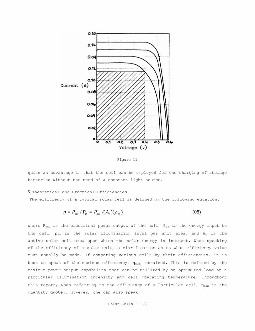
Figure 11
quite an advantage in that the cell can be employed for the charging of storage
batteries without the need of a constant light source.
5. Theoretical and Practical Efficiencies
The efficiency of a typical solar cell is defined by the following equation:
(08) ))(/(/ incoutinout APPP ρη ==
where Pout is the electrical power output of the cell, Pin is the energy input to
the cell, ρin is the solar illumination level per unit area, and Ac is the
active solar cell area upon which the solar energy is incident. When speaking
of the efficiency of a solar unit, a clarification as to what efficiency value
must usually be made. If comparing various cells by their efficiencies, it is
best to speak of the maximum efficiency, ηmax, obtained. This is defined by the
maximum power output capability that can be utilized by an optimized load at a
particular illumination intensity and cell operating temperature. Throughout
this report, when referring to the efficiency of a Particular cell, ηmax is the
quantity quoted. However, one can also speak
Solar Cells -- 19

of the operating efficiency, eL op; the efficiency at which the solar cell or array is
actually being utilized. This quantity is useful when comparing units operating at a
less than maximum output.
Figure 12
Equation 8 is very useful in calculating the practical efficiencies of various
types of solar cells. Although 20% efficiencies have been achieved in the laboratory
under strictly controlled optimum conditions, under normal operating conditions, the
cell efficiencies vary from 10% for an OCLI Conventional silicon solar cell to 15% for a Comsat non-reflecting, p+ , textured silicon solar cell. Thus far, it seems the most
efficient per unit cost solar cell available today is that produced with silicon even
though other cells made with different materials have comparable efficiencies. However,
these cells on the whole, are more costly to produce commercia11y .
According to theory, the maximum theoretical efficiency obtainable from silicon
solar cell is approximately 22%. This value results from an analysis of the equation
for the maximum solar conversion efficiency;
avph
mpGph
mp
mp
ENVEn
VV
k)(
)1
(max ⋅+
=λ
λη
where k is a constant depending on the reflection and transmission coefficients
Solar Cells--20

and the collection efficiency, Vmp is the voltage delivered at maximum power,
nph(Eg) is the number of photons that generate EHP's in a semiconductor of
energy gap Eg, and NphEav is the input power where Nph is the number of incident
photons and Eav is their average energy in electron volts. Assuming λVmp» 1 and
k ≅ 1, this equation reduces to :
(10) )(
maxavph
mpgph
ENVEn
≅η
By further assuming that for silicon, nph ≅ (2/3) Nph and Vmp ≅ (1/3)Eav, the
equation yields:
(11) %2292)3/1()3/2(
max ==≅avph
avph
ENEN
η
In a report written by M.B. Prince and published in 1955, this value was
determined to be approximately 21.7%. This is considered the ultimate maximum
theoretical efficiency obtainable for a silicon solar energy converter. An
interesting note here is that if mono-chromatic light is used with an energy
equal to the band gap, nph will be equal to Nph and Vmp = .75 Eav, therefore, the
maximum theoretical efficiency could be approximately 75%. As is evident from
the equation for ηmax, the theoretical maximum efficiency is a function of the
semiconductor energy gap. Although for increasing values of the energy gap, the
number of photons absorbed decreases, because Io is also reduced, the cell
voltage is thus increased. Shown in figure 13 is a graph illustrating the
relation between ηmax and Eg for several solar cell materials.
In terms of efficiency versus band gap, cadmium telluride (CdTe) appears
to be the best suited material for producing photovoltaic devices. However,
due to a combination of low electron mobilities (thus resulting in poor
collection efficiencies) coupled with a high internal resistance, the prac-
tical efficiencies obtained to date for this material have been less than 8%
under ordinary operating conditions. When comparing the efficiency per
Solar Cells -- 21

unit cost of CdTe cells to that of silicon, silicon cells hold a distinct
advantage over CdTe.
On the other hand, InP has high electron mobilities and laboratory
efficiencies have been achieved that are competitive with silicon ( = 12%).
However, here too, silicon possesses a much greater efficiency when
considering cost aspects as InP solar cells axe still quite expensive to
produce commercially.
Figure 13
Perhaps the most promising material other than silicon for producing solar
cells is Gallium Arsenide (GaAs). Possessing an energy gap close to the peak of
the curve in figure 13, and an electron mobility higher than that of silicon,
this material has the potential for replacing silicon as the most common
photovoltaic material. Even though this type of material has its drawbacks,
such as a minority carrier lifetimes and an absorption coefficient much lower
than for silicon, practical efficiencies of 14% have been reported (very
comparable to Si). Although at present, GaAs is a very
Lifetime: the average time between EHP creation and recombination.
Solar Cells -- 22
expensive material; Ga and As material costs have been decreasing steadily and
it is predicted that by 1990, the material costs of Si and GaAs will probably
be equal thus making GaAs solar cells extremely competitive with Si cells.
Although as of late, higher maximum solar energy conversion efficiencies
have been obtained, the percentage increase has not been substantial due to the
many factors on which the efficiency depends. Since not all of the desired
specifications can be met in the design of a solar cell, trade-offs must be
made in order to yield the highest efficiency unit at a reasonable cost. In
general, the maximum solar efficiency depends upon the following
factors: -the solar cell internal construction,
-dimension,
-active area,
-specific material properties,
-photovoltaic junction characteristics,
-the anti-reflective coating,
-surface texture,
-contact and grid configuration,
-the illumination', level,
-cell operating temperature,
-and various environmental factors.
6. Effects of Temperature and Internal Resistances on Cell Efficiency
One should expect any device utilizing semiconductors to be quite sensitive
to temperature deviations from normal operating temperatures, and solar cells
are no exception. An increase in the operating temperature of a solar cell
typically has the effect of slightly increasing the cell's short-circuit
current and significantly decreasing the cell voltage. Therefore, as the
temperature of the solar cell rises, the result is that the maximum efficiency
decreases. (the area of the power rectangle under the VI curve decreases). In a
silicon solar cell, the short-circuit current is relatively independent of
temperature, being only a function of the illumination level. Thus, the
increase in ISC, typically less than 0.1%/°C, depends only
Solar Cells--23

upon the spectral distribution of the illuminating light and the spectral
response of the solar cell. The cell voltage, however, decreases substantially
for increasing cell temperatures due to changes in the diode conduction
characteristics; in other words, V is a function of Io, a quantity quite
sensitive to temperature changes. Typically, the voltage usually decreases at a
rate of approximately 2.0 - 2.3 mV/°C.
For the silicon solar cell used in this experiment, the temperature
coefficients are as follows:
Temperature Range: -65°C to +125°C
Voltage: increases by 2mV/°C below 25°C
decreases by above
Current: increases by 25 A/cm2/°C above 25°C
decreases by below Power: decreases by 0.3%/°C above 25°C
increases by below
Because a typical solar cell contains internal resistances that can reduce
the cell's maximum efficiency dramatically, the simplified circuit in figure 8
can be modified as illustrated in figure 14 to show these internal resistances.
Figure 14
In the above figure, RS is the cell's series resistance and Rsh is the shunt
resistance. The solar cell's series resistance represents in lumped fashion all
distributed resistance elements in the device, its ohmic contacts, and the
semiconductor/contact interfaces. Because RS is a lumped quantity, it varies
with practically every cell parameter, such as the VI characteristic,
Solar Cells--24

illumination level, and temperature. The solar cell's shunt resistance, on the
other hand, represents the portion of the generated electrical energy lost
through the cell's internal leakage paths such as that through the p-n junction
(recombination current), and along the outer cell edges (surface leakage).
Both of the solar cell internal resistances effect the output of the solar
unit, however, for operation with illumination near one solar constant, the
effect of the shunt resistance is negligible. The series resistance, though,
has a dramatic effect on the output and thus the energy conversion efficiency
of the solar cell. Ideally, it is desired that the series resistance approach
zero while the shunt resistance approaches infinity. As an example, a shunt
resistance as low as 100 ohms does not appreciably change the shape of the VI
curve (and thus the power output) of a cell whereas a series resistance of only
5 ohms reduces the available load power to less than 3096 of the optimum power
with Rs = 0 ohms. The effect of both Rs and Rsh on the VI characteristic curve
for a 2 x 2 cm solar cell is shown in figure 15 .
Figure 15
Solar Cells --25

7. Practical Realizations
It can hardly be said of photovoltaics that their day has arrived. However,
in the comparison of solar cells versus conventional means of generating
electricity, it is obvious that solar energy converters are gaining ground
rapidly ( as natural resources dwindle and costs soar) and in the long run will
most likely either come out on top or at least be a competitive energy source
in the future. As with all new technologies, it takes time and effort before
any practical applications can be realized. Throughout the world, this effort
is being put forth in the form of advanced research on photovoltaic systems and
hence it is only a matter of time before the day of the solar cell is upon us.
i. Applications
Although the cost of solar energy is still too expensive, yielding power
ten times more costlier than that generated by oil, there are still
applications for which solar power is economically feasible. It is particularly
suited for remote applications where there is no direct tie-in to an electric
utility feeder, or where the transportation of fuel to the generator site is
impractical. In conjunction with an electrochemical storage battery and
suitable charge control electronics, solar cell arrays can be designed to
provide practically continuous power. Some examples of this type of application
include:
1. electronic and optical beacons and warning devices such as
channel buoys and shoreline barkers.
2. remote television and radio receiver stations.
3. radio transmitters and transponders, microwave repeater
stations.
4. weather and earthquake monitoring stations.
5. electronic (galvanic) corrosion protection of metal structures
such as bridges and towers.
With the assistance of federally funded programs, numerous other practical
Solar Cells--26

applications are then made economically feasible. Some of these applications
include:
1. solar panels installed on the rooftops of homes can provide
either heating and hot water or a percentage of the total
electricity consumed.
2. solar panels installed on the rooftops of commercial and public
buildings can provide can provide a portion of the total
electricity consumed; some examples where implementation has
already occurred include a national park headquarters, some
schools, and a daytime country music station in Ohio.
3. irrigation projects.
4. use of solar cells for hydrolysis and other electrochemical
processes.
5. emergency, surveillance, and security systems.
Although the applications noted above can be termed small scale, large
scale solar generating stations have been proposed but due to the efficiency
limitations 2nd the high per watt cost of these pmts, it does not appear that
these proposals will be economically feasible and therefore, not realized for
quite awhile. However, it is worthwhile to examine a typical solar energy
generating scheme in order to get an idea of how to power from large solar
arrays will interface with the conventional power grid. The basic block
diagram far a typical solar power generating system is shown in figure 16 .
The basic operation is quite simple, beginning with the power generation
by the solar array. By employing an array orientation system, the array output
capability is maximized by having this subsystem orient t-a solar cells at the
right angle to the sun during all operating periods. The generated power is
then gathered by a power collection system which then routes a portion of the
power to an energy storage system and the rest to the conversion/regulation
system. The energy storage is necessary to provide electricity dozing periods
when the soles array is not sufficiently illuminated to generate a, usable
output. The power proceeding to the c/r subsystem
Solar Cells--27

is then "smoothed" and fed into a distribution center which reroutes a portion of
this usable back into the system for control purposes, The remainder is then fed
into the main power grid via an interfacing system and distributed to the various
user loads.
Figure 16
Even though at this time, this type of large scale solar energy generation
is not economically feasible, the prospects far a system of this type in the
future are excellent and should not be ignored.
Because solar cells consume no fuel, do not emit harmful exhaust products or
radiation, and operates with little or no maintenance for a long period of time, they are
especially well suited for applications in the space industry. This is apparent in that
most of the satellites and space
Solar Cells --28

vehicles launched to date have utilized power from on-board solar cell arrays
to operate the internal equipment as well as the communication equipment. In
addition, recently a new area under investigation is that of solar-electric
propulsion for space vehicles. The basic concept is that high voltage electric
energy produced by a solar cell array is utilized by an ion drive to ionize a
substance and to eject a stream of ionized particles which propels the
spacecraft in a manner similar to a rocket engine. Although still in the
planning stages, it nonetheless conveys the idea that in the future, solar
cells will be doing more than just providing electricity for our homes.
ii. Concentrators
For many photovoltaic applications, it may be desirable to improve the
output of the solar cell by the use of solar concentrators. The purpose of the
concentrator is to increase the intensity of the sunlight incident on the cell
over its naturally occurring value thus increasing the cell output by a
proportional amount. Solar concentrators can be described on the basis of their
"geometric concentration ratio,"
tag AAC /=
where Aa is the entrance aperture area and At is the smaller target area or exit
aperture area. However, because of optical imperfections in most concentrators,
it is best to relate the performance of a concentrator by its "actual
concentration ratio,"
gita CSSC 0/ η==
where St is the solar intensity incident on the target plane, Si is the solar
intensity incident on the entrance aperture, and η0 is the concentrators
optical efficiency. Because solar intensity measurements are very time
consuming and difficult to obtain accurately, it is preferable to utilize an
equation relating the overall concentrator/ array system efficiency.
Solar Cells--29

This is given by:
(14) / aaouts ASP=η
where Pout is the cell output power in watts, Sa is the solar intensity
incident on the entrance aperture of the concentrator, and Aa is the entrance
aperture area in square meters. This is experimentally obtainable although
care must be taken to assure accurate measurements of Sa.
Basically, there are five methods in which sunlight can be concentrated:
refraction, reflection, wavelength conversion , diffraction, and laser action;
with the first two cases being the most popular methods. Reflection is usually
accomplished by the use of mirrors whereas refraction is done with lenses. In
this experiment, Fresnel concentrator lenses will be used to refract the light
although other types of lenses such as planoconvex, and bioconvex can also be
used.
iii. Lifetime and Maintenance
In essence, solar cells have unlimited life and are practically
maintenance free. However, since the cells are usually subject to various
environmental effects, both fair and adverse, photovoltaic systems do require
some periodic maintenance (especially for terrestial applications) so that
negligible cell or system degradation occurs.
Humidity is perhaps the major cause of most maintenance problems for solar
arrays, causing the growth of fungus and the formation of a "sticky" surface
film that tends to catch dust and dirt particles. This in turn leads to
reduced cell output and lower efficiencies. Humidity, coupled with high
temperatures is also very detrimental in that corrosion occurs.
In addition to humidity problems, other environmental effects on arrays
that may require some preventive maintenance is that occuring by various forms
of precipitation (especially hail, snow, and ice; rain has a beneficial
effect), by wind damage, earthquakes, and unfortunately, vandalism.
Solar Cells--30
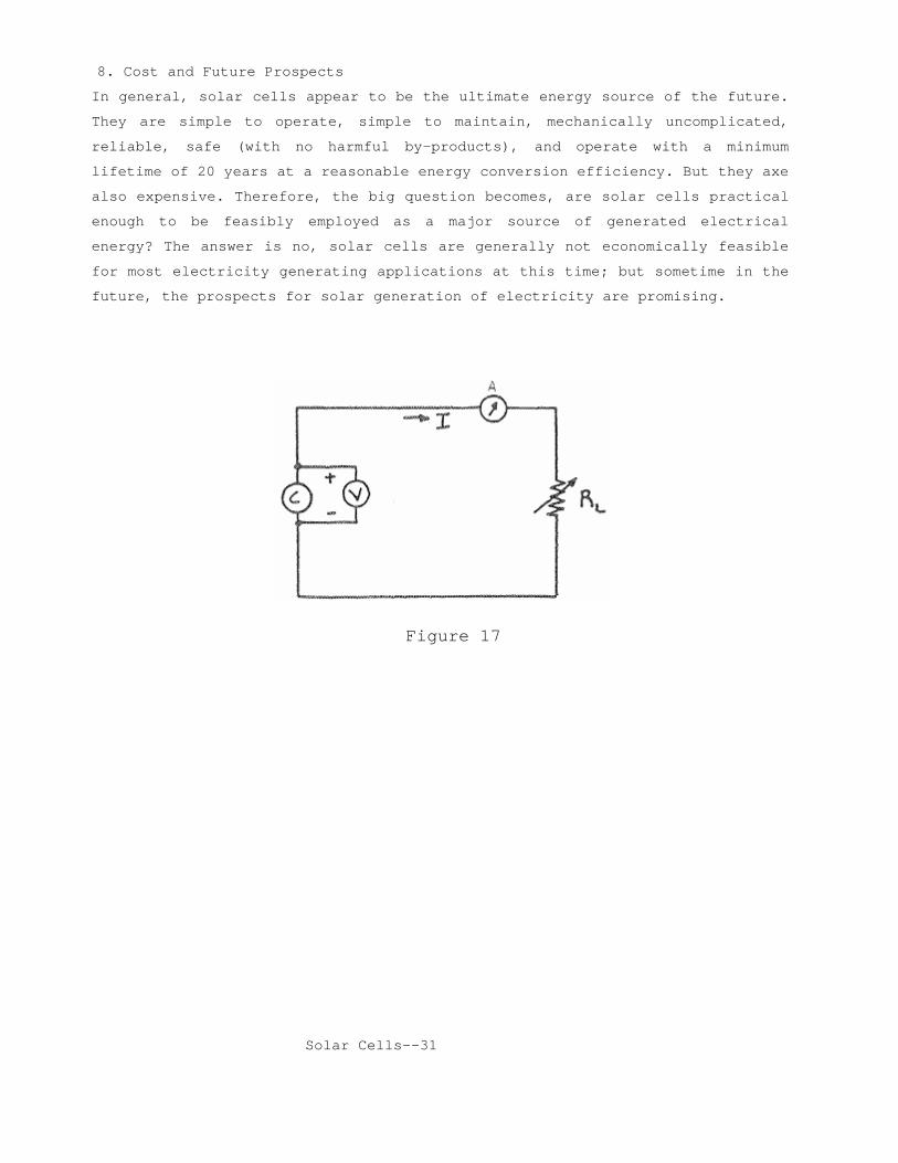
8. Cost and Future Prospects
In general, solar cells appear to be the ultimate energy source of the future.
They are simple to operate, simple to maintain, mechanically uncomplicated,
reliable, safe (with no harmful by-products), and operate with a minimum
lifetime of 20 years at a reasonable energy conversion efficiency. But they axe
also expensive. Therefore, the big question becomes, are solar cells practical
enough to be feasibly employed as a major source of generated electrical
energy? The answer is no, solar cells are generally not economically feasible
for most electricity generating applications at this time; but sometime in the
future, the prospects for solar generation of electricity are promising.
Figure 17
Solar Cells--31

9. References
1. Magid, Dr. L. MI., Dr. P. Rappaport, Prospects and Opportunities in
Photovoltaics, 2nd E.C. Photovoltaic Solar Energy Conference, D.
Reidel Publishing Co., Boston, 1979
2.Prince, M.B „ Silicon Solar Energy Converters, Solar Cells, (Journal of
Applied Physics), IEEE Press, New York, 197
3.Rappaport, P., The Photovoltaic Effect and Its Utilization, Solar Cells,
(RCA Review, Sept. 1959), IEEE Press, New York, 1976
4. Rapport, P., Single-Crystal Silicon, Solar Cells, (Proceedings of the
Workshop on Photovoltaic Conversion of Solar Energy for Terres trial
Applications, Volume I, Working Group and Panel Reports, Oct. 1973), IEEE
Press, New York, 1976
5. Rauschenbach, H.S., Solar Cell Array Design Handbook, Van Nostrand
Reinhold Co., New York, 1980
6.Rauschenbach, H., M. Wolf, Series Resistance Effects on Solar Cell
Measurements, Solar Cells, (Advanced Energy Conversion, April-June 1963),
IEEE Press, New York, 1976
7. Solomon, B., Will Solar Cell?, Science 82, American Association for the
Advancement of Science, April 1982
8. Streetman, B.G., Solid State Electronic Devices, second edition, Prentice-Hall, Inc., Englewood Cliffs, New Jersey, 1980
Solar Cells -- 32

B. EXPERIMENT 1. Equipment List
1 Instrument rack with the usual test equipment
1 Mounted silicon solar cell (Solarex #42,270)
1 Radiometer
1 G.E. Quartzline Halogen lamp (Par Flood Lamp, Q150Par 38FL)
1 Mounted outdoor lamp fixture (Sarama 2953 - 15)
1 Variable autotransformer
1 Temperature probe
1 Roll masking tape
1 Meter stick
? such other equipment as may be needed
2. Preliminary Setup and Calibration
To assist the student in his endeavors, the solar cell has been mounted in a convenient box and
suitable resistors permanently connected as shown in Fig. 18. Pay special attention to the two
potentiometers which (a) increase resistance when their knobs are rotated in a clockwise direction
and (b) together with the shunt constitute the load resistance RL. Note that the contact resistance
in each should be on the order of 10 mΩ. Electrical connections to the solar cell must be made as
illustrated in Fig. 18; this is known as a 'four-wire connection' and minimizes the effects of lead
and contact resistance in the measurements.
Figure 18 Solar Cells -- 33

Use masking tape to mark a zero position for the front face of the solar cell box
close to the equipment chassis and perpendicular to the edge of the bench. Lay down
strips of masking tape from the zero position to the far end of the bench; these tape strips
should be parallel to the edge of the bench. Calibrate the tape strips at 0, 100, 250, 500,
750, 1000, 1250, and 1500 mm. Note that the optical axis of the solar cell lies 90 ± 5 mm
above the bench top.
Connect the infrared (IR) sensor to the light meter to form a radiometer. Calibrate
the radiometer in units of W/m2 per the calibration procedure using the coefficient shown
on the IR sensor tab. Now tape the IR sensor to the back of the solar cell box, centered
left to right, 90 ± 5 mm above the bench top. Position the solar cell box with the IR sensor
facing the flood lamp such that the IR sensor face is on the marked zero position
3. Incident IR Energy Connect the flood lamp to a variable autotransformer and adjust the lamp voltage
to the maximum that allows incident power readings to be taken at 100 mm without
saturating the radiometer. Be sure that ambient IR energy is minimized by turning off all
bench lights and closing all blinds. With the flood lamp off, record the ambient IR reading.
Now turn the flood lamp back on and measure incident power density at the solar cell box
position in kW/m2 as a function of radiometer to lamp spacing at each calibrated distance.
4. Solar Cell VI Characteristics
With the incident illumination set to a nominal# 1 kW/m2 through adjustment of the lamp spacing
only, face the solar cell box toward the flood lamp with its front at the zero position. Vary RL and
measure v(i) all the way♥ from near-open-circuit to near-short-circuit conditions. 5. Solar Cell Sensitivity
Adjust RL to yield three-quarter maximum current at the illumination of 1 kW/m2 ; call this value
RL*. Then determine v and i at RL
*, at RL = near-open-circuit, and at RL = near-short-circuit
for a number of different illuminations at the calibrated distances as the flood lamp position is
varied all the way from 100 mm to 1500 mm. # "nominal" is a superb weasel-word which should be mastered by all practicing engineers and scientists. What it means is that the quantity in question has been measured to the best of our ability but that we aren't prepared to say just how great our ability is. Presumably, (i) a sequence of nominal values will correlate well with the corresponding sequence of actual values. (ii) the absolute error of any measurement is within bounds considered tolerable by an experienced investigator in the area, and (iii) any given setting or measurement is repeatable. ♥ In varying Ri, proceed with delicacy. You'll have a devilish time finding the power maximum unless you employ sharp ears and sensitive Fingertips to discern the winding-to-winding progress of the wiper over the coils of the rheostat..
Solar Cells -- 34
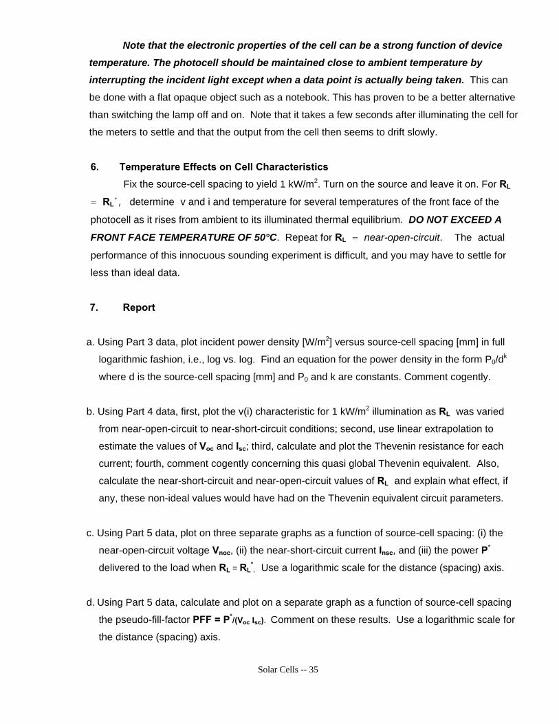
Note that the electronic properties of the cell can be a strong function of device
temperature. The photocell should be maintained close to ambient temperature by
interrupting the incident light except when a data point is actually being taken. This can
be done with a flat opaque object such as a notebook. This has proven to be a better alternative
than switching the lamp off and on. Note that it takes a few seconds after illuminating the cell for
the meters to settle and that the output from the cell then seems to drift slowly.
6. Temperature Effects on Cell Characteristics Fix the source-cell spacing to yield 1 kW/m2. Turn on the source and leave it on. For RL
= RL*, determine v and i and temperature for several temperatures of the front face of the
photocell as it rises from ambient to its illuminated thermal equilibrium. DO NOT EXCEED A
FRONT FACE TEMPERATURE OF 50°C. Repeat for RL = near-open-circuit. The actual
performance of this innocuous sounding experiment is difficult, and you may have to settle for
less than ideal data.
7. Report
a. Using Part 3 data, plot incident power density [W/m2] versus source-cell spacing [mm] in full
logarithmic fashion, i.e., log vs. log. Find an equation for the power density in the form P0/dk
where d is the source-cell spacing [mm] and P0 and k are constants. Comment cogently.
b. Using Part 4 data, first, plot the v(i) characteristic for 1 kW/m2 illumination as RL was varied
from near-open-circuit to near-short-circuit conditions; second, use linear extrapolation to
estimate the values of Voc and Isc; third, calculate and plot the Thevenin resistance for each
current; fourth, comment cogently concerning this quasi global Thevenin equivalent. Also,
calculate the near-short-circuit and near-open-circuit values of RL and explain what effect, if
any, these non-ideal values would have had on the Thevenin equivalent circuit parameters.
c. Using Part 5 data, plot on three separate graphs as a function of source-cell spacing: (i) the
near-open-circuit voltage Vnoc, (ii) the near-short-circuit current Insc, and (iii) the power PP
*
delivered to the load when R = RL L*.
Use a logarithmic scale for the distance (spacing) axis.
d. Using Part 5 data, calculate and plot on a separate graph as a function of source-cell spacing
the pseudo-fill-factor PFF = P*/(Voc Isc). Comment on these results. Use a logarithmic scale for
the distance (spacing) axis.
Solar Cells -- 35

e. Determine the efficiency of the solar cell at 200 mm source-cell spacing based on the measured
IR energy from Part 3 and the v and i data at RL* from Part 5. Assume the diameter of the solar
cell is 2.75 inches. Comment on this value of efficiency.
f. Using Part 6 data, reduce your results to produce curves of near open circuit voltage Vnoc and
Thevenin resistance versus temperature. Comment cogently and concisely.
g. Consider the simplified equivalent circuit shown in Fig. 19 for a solar cell under test. Presume that the
current generator represents the solar current IS [A] and that the diode current is given by
]1[0 −= κeIiD
where IO is a constant scale current and, as might be expected, K = eVD/kT. Show that the short
circuit current is the solar current, i.e., Isc = IS, and that the open circuit voltage VOC is given by
]1ln[0
+=II
ekTV S
oc
h. Next prove (or disprove) the assertion that the power to the load PL is given by
]}1[{ 0 −−= κeIIVP SDL
IL
i. Derive a formula for the fill factor as a function of VD and then differentiate it to find the value of VD
for which the fill factor is a maximum for a particular IS .
Solar Cells -- 36
Figure 19.
VDIIS iD VD