solar cells, modules, arrays, and...
TRANSCRIPT

.... energizing Ohio for the 21st Century
April 17, 2014
The University of Toledo, Department of Physics and Astronomy
SSARE, PVIC
Principles and Varieties of Solar Energy (PHYS 4400)
Solar Cells, Modules, Arrays, and
Characterization

.... energizing Ohio for the 21st Century
Solar Cells – current and voltage
Wiring up a c-Si solar module – typical current and voltage
Wiring up a CdTe module
An example of a PV Array – 6 kW system
Techniques for characterizing photovoltaic materials, cells, and modules
Topics

.... energizing Ohio for the 21st Century
Getting everything right…
~ 33%

.... energizing Ohio for the 21st Century
monocrystalline Si solar cell

.... energizing Ohio for the 21st Century
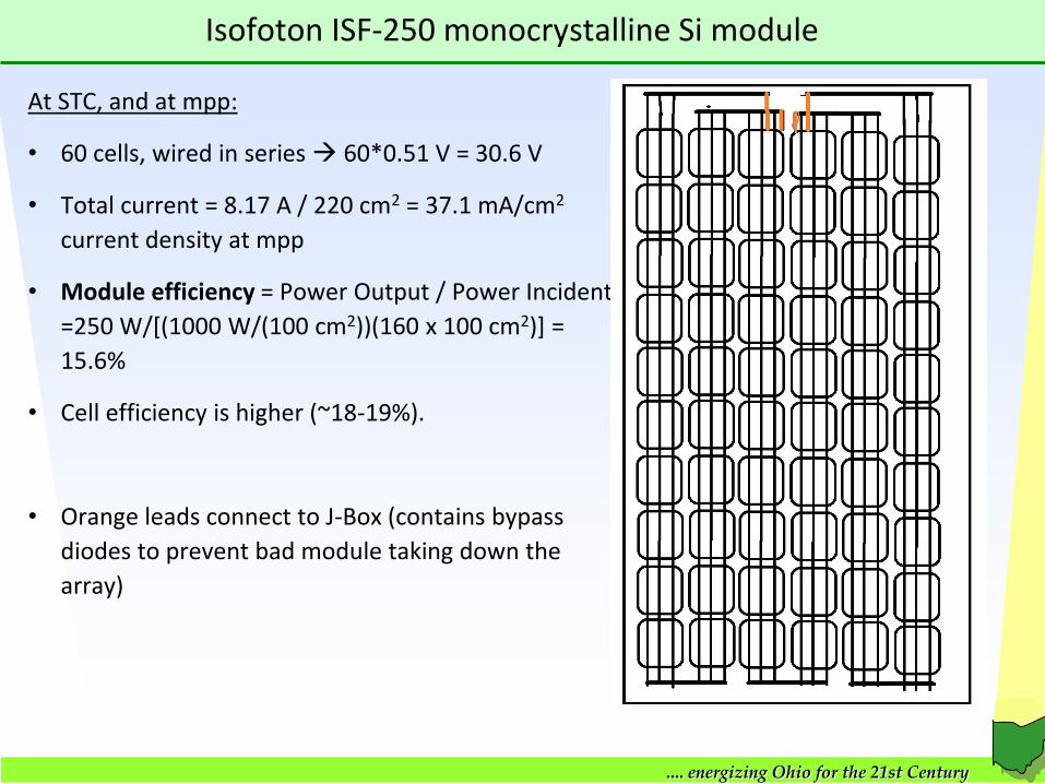
Isofoton ISF-250 monocrystalline Si module
.... energizing Ohio for the 21st Century
Isofoton ISF-250 monocrystalline Si module
At STC, and at mpp:
• 60 cells, wired in series 60*0.51 V = 30.6 V
• Total current = 8.17 A / 220 cm2 = 37.1 mA/cm2
current density at mpp
• Module efficiency = Power Output / Power Incident
=250 W/[(1000 W/(100 cm2))(160 x 100 cm2)] =
15.6%
• Cell efficiency is higher (~18-19%).
• Orange leads connect to J-Box (contains bypass
diodes to prevent bad module taking down the
array)

.... energizing Ohio for the 21st Century
CdTe Solar Cell
At STC, and at mpp:
• For record device, JSC is higher, 28 mA cm-2
• VOC also higher, 0.880 V
• With FF = 0.77, 19%

.... energizing Ohio for the 21st Century
CdTe Module (First Solar FS-390)

Photoluminescence Lifetime System Specifications
Free Space Beam Height: AOTF: 26 mm (may need a periscope) iHR320: 98mm (from bottom of instrument) Temporal Pulse Width of the Fianium: ~5 ps Excitation Wavelength Range: <420 nm to >2 μm from the light source, and 400 nm-1100 nm from the Frequency Tuner. Detection Wavelength Range: Hamamatsu H10330A-45 NIR PMT: 950 - 1400 nm Hamamatsu R10467U-50 Hybrid PD: 380 - 890 nm Transit Time Spread: H10330A-45 NIR PMT: 400 ps, Rise/Fall: 900 ps/1.7 ns, R10467U-50 Hybrid PD: 90 ps, Rise/Fall: 400/400 ps, Width: 600 ps Pulse Repetition Rate: 20 MHz, 10 MHz, 5 MHz, 2 MHz, and 1 MHz Pulse Energy: ~0.25 nJ/(5 nm Channel) @ 20 MHz, or 2 nJ with all 8 channels.

Fianium Super-
Continuum Light Source
AOTF NIR Vis
iHR320
TCSPC
Electronics
Laser Sync
Laptop
Photon Counts
Sample holder and/or cryostat
Sample
300ps Laser Pulse
T=0
Voltage
T=0 Sample
PL Emission Pulse τ > 300ps
T=0
Voltage
T>0
To iHR320
T=0 : The sync from the laser is registered in
the Time to Amplitude Converter.
T>0 : Photons emitted from the sample reach
the detector and are counted. Their count
time is found from the voltage of the count.
T>>0 : This is repeated millions of times per
second and a histogram depicts the photons
collected as a function of time from the sync.
Time Correlated Single Photon Counting
Laser Pulse

Sample PL Lifetime Data
CdTe solar cells are understood to benefit from crystal quality correlated with increased minority carrier lifetime. The minority carrier lifetime can be measured using time-resolved PL, since the PL intensity depends on the product of the free electron and free hole concentrations:
),(),(, tEptEnEtIPL
TRPL measurements from untreated (as-deposited) CdTe are a good test of a PL lifetime system’s sensitivity because emission intensity is quite low at room temperature. The above graph shows the PL lifetime data for treated vs. untreated CdTe at a fixed excitation pulse energy. The activated CdTe film shows an increase in the peak PL intensity of ~10x, and an increase in the lifetime by ~10x. Together these factors yield a strong increase in the time-integrated PL inetnsity (not shown).

.... energizing Ohio for the 21st Century
Measuring bandgap (PL)
Photoluminescence (occurs at the bandgap for direct gap semiconductors)
Bandgap can also be measured with: • SPS – surface photovoltage spectroscopy • Spectroscopic ellipsometry (?)
Pushing the Band Gap Envelope: Mid-Infrared Emitting Colloidal PbSe Quantum Dots, J. AM. CHEM. SOC. 2004, 126, 11752-11753, Hollingsworth et al.

X-Ray Diffraction Structural properties

X-rays are electromagnetic radiation with wavelength ~1 Å = 10-10 m (visible light ~5.5x10⁻⁷ m)
X-Ray Generation
X-ray generation: electrons are emitted from the cathode and accelerated toward the anode. Here, Bremsstralung radiation occurs as a result of the “braking” process – X-ray photons are emitted.
X-ray wavelengths too short to be resolved by a standard optical grating
1 11 0.1 nm
sin sin 0.00193000 nm
m
d

The most common metal used is copper, which can be kept cool easily, due to its high thermal conductivity, and which produces strong Kα and Kβ lines. The Kβ line is sometimes suppressed with a thin (~10 µm) nickel foil.
X-Ray Generation
Atomic levels involved in copper Kα and Kβ emission.
• K-alpha (K) emission lines result when an electron transitions to the innermost "K" shell (principal quantum number 1) from a 2p orbital of the second or "L" shell (with principal quantum number 2). • The K line is actually a doublet, with slightly different energies depending on spin-orbit interaction energy between the electron spin and the orbital momentum of the 2p orbital.
from http://en.wikipedia.org/wiki/K-alpha
(K) = 0.154 nm
(K) = 0.139 nm


Diffraction of x-rays by crystal: spacing d of adjacent crystal planes on the order of 0.1 nm
→ three-dimensional diffraction grating with diffraction maxima along angles where reflections from different planes interfere constructively
X-Ray Diffraction -- Bragg’s Law
2d sin = m for m = 0, 1, 2, …
Bragg’s Law
Note that your measured XRD spectra will most likely reveal only 1st order diffracted lines (i.e., those for which m = 1).

Interplanar spacing d is related to the unit cell dimension a0
X-Ray Diffraction, cont’d
2 050 04
5 or 0.223620
ad a d a
Not only can crystals be used to separate different x-ray wavelengths, but x-rays in turn can be used to study crystals, for example determine the type of crystal ordering and a0.

X-Ray diffraction (XRD) pattern (diffractogram) from NaCl
222
0
lkh
adhkl
http://web.pdx.edu/~pmoeck/phy381/Topic5a-XRD.pdf

Raw Data
Peaks were considered if they were known CdTe peaks. Peaks from other layers (ex. CdS) were not included.

J-V and Spectra Response Characterization

p-type emitter (window) n-type base (absorber)
n-type emitter (window) p-type base (absorber)
Vbi
+ - + -
+J under forward bias
Homojunction solar cell (e.g., Silicon)
+J under forward bias
+ -
J/V?
+
-
J/V?
Before contact
At equilibrium
+J
+V
hν JL JL
JL
JL
Light Generated Current is Opposite Direction of Forward Dark Current
Typical Si device configuration

Solar cell efficiency
The efficiency of a solar cell (sometimes known as the power conversion efficiency, or PCE, and also often abbreviated η) represents the ratio where the output electrical power at the maximum power point on the IV curve is divided by the incident light power – typically using a standard AM1.5G simulated solar spectrum.
The efficiency of a solar cell is determined as the fraction of incident power which is converted to electricity and is defined as:
FFIVP SCOCmax
where Voc is the open-circuit voltage; where Isc is the short-circuit current; and where FF is the fill factor where η is the efficiency. Power in AM1.5G spectrum is 1kW/m2 , or 100 mW/cm2
For a 10 x 10 cm2 cell, the input power (AM1.5G) is 100 mW/cm2 x 100 cm2 = 10 W.
inc
SCOC
P
FFIV

Impact of Electrical Loss Due to High Series Resistance (RS) PV cells
Cu
rren
t d
en
sity
(m
A/c
m2)
Volts (V)
Diode equation with RS and RSH:
RSH = 10,000

Solar cell series and shunt resistance
From http://www.pveducation.org/pvcdrom/solar-cell-operation/series-resistance
Series resistance (RS) in a solar cell has three causes: (1) the movement of current through the front contact
and the semiconductor absorber region of the solar cell; (2) contact resistance between the metal contact and
the silicon; and (3) resistance of the top and rear metal contacts. A high series resistance reduces the fill factor,
and excessively high values may also reduce the short-circuit current.
Significant power losses caused by the presence of a shunt resistance (Rsh) are typically due to
manufacturing defects, rather than poor solar cell design. Low shunt resistance causes power losses in solar
cells by providing an alternate current path for the light-generated current.
We have measured I vs. V,
so that for I in Amps and V
in Volts, the apparent
resistance () at any point
on the curve is given by:
(-1)/slope. The shunt
resistance is defined at V =
0 V, and the series
resistance is defined at V =
VOC. For optimal power
generation, solar cells
should have a large Rsh
and a small RS.
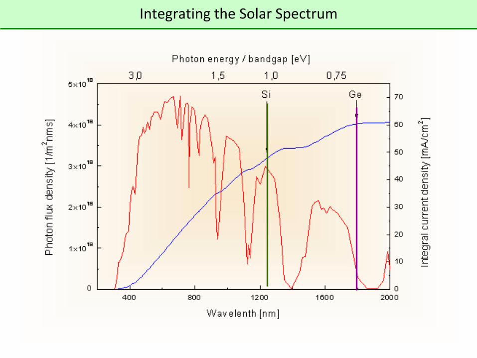
Integrating the Solar Spectrum

Spectral Response of a typical c-Si solar cell
http://en.wikipedia.org/wiki/File:Solarcellige-en.svg

.... energizing Ohio for the 21st Century
UT’s Laser Scriber System
• 3 wavelengths (1064 nm, 532 nm, 355 nm) for addressing specific materials based on absorption spectrum.
• 60 cm x 60 cm flat field based on z-focus.

.... energizing Ohio for the 21st Century
UT’s Laser Scriber System
• Sample mounts; Motion control
• Exhaust handling (HEPA)

.... energizing Ohio for the 21st Century
LBIC, LBIV
• Laser Beam Induced Current
• Laser bean induced Voltage
• Reveals cell layout for CdTe PV modules

.... energizing Ohio for the 21st Century
• CdTe mini-module, illuminated with 532 nm laser spot (~40 m diameter)
• Lateral resistance across the back contact
• Scratch on cell #7
LBIC of CdTe mini-module

.... energizing Ohio for the 21st Century
Achieve charge separation
Achieve charge separation, directing electron and holes to different contacts (e.g., use doped materials for p-n junction)… Prepare your materials and junctions to establish a built-in electric field. How?
Homojunction: (junction between two layers of the same material, which can differ by doping, structure, etc. but show the same dominant elemental makeup) -- must vary the chemical potential of the material (Fermi level) across the interface between n-type and p-type.

.... energizing Ohio for the 21st Century
Achieve charge separation
Achieve charge separation, directing electron and holes to different contacts (e.g., use doped materials for p-n junction)… Prepare your materials and junctions to establish a built-in electric field. How?
Heterojunction: (junction between two different semiconductor materials) -- must create an energy band structure that promotes charge separation – a combination of energy band offsets and doping.
How do we measure the dopant type and density?

.... energizing Ohio for the 21st Century
Measuring dopant type and density
Hall Effect: The Lorentz force, F = -qv x B, deflects carriers to the left and right as they pass through a material under the influence of a magnetic field. The induced voltage lateral to the current flow direction provides information about the Hall coefficient, which can then be related to the carrier density and mobility:
Preston and Dietz, (Expt. 17; pp 303-315)
HeRn
1
HR
zx
y
HBJ
ER

.... energizing Ohio for the 21st Century
Measuring dopant type and density (Mott Schottky)
Mott-Schottky: measuring in depletion, not in accumulation. Changing the depletion width by applied voltage; when the capacitance reaches a maximum flat band potential.
dW
A
V
QC
Sign of slope determined by free carrier type; slope related to free carrier density
http://www.currentseparations.com/issues/17-3/cs-17-3d.pdf

.... energizing Ohio for the 21st Century
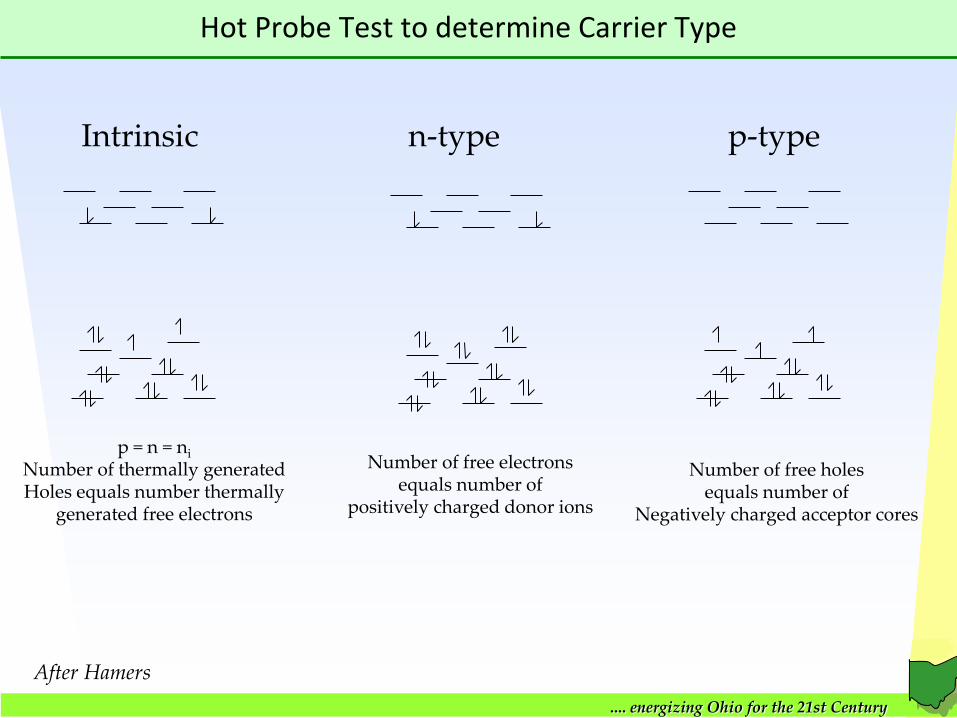
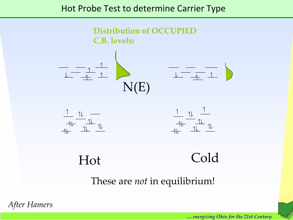
Hot Probe Test to determine Carrier Type
Seebeck Effect • In 1821, Thomas Seebeck discovered that an electric current
would flow continuously in a closed circuit made up of two dissimilar metals if the junctions of the metals were maintained at two different temperatures.
• When a metal wire is connected between two different temperatures, an additional number of electrons are excited at the hot end versus the cold end.
• Electrons drift from the hot end to the cold, and • A thermal emf develops to oppose the drift • If the material is uniform, the magnitude of the voltage
developed depends only on the temperature difference. • The Hot Probe is the trivial case……i.e., no junctions.

.... energizing Ohio for the 21st Century
Hot Probe Test to determine Carrier Type
All you need is a soldering iron, and an ammeter!
http://ecee.colorado.edu/~bart/book/hotprobe.htm
.... energizing Ohio for the 21st Century
Hot Probe Test to determine Carrier Type
p = n = ni Number of thermally generated Holes equals number thermally
generated free electrons
Number of free electrons equals number of
positively charged donor ions
n-type
p-type
Intrinsic
Number of free holes equals number of
Negatively charged acceptor cores
After Hamers
.... energizing Ohio for the 21st Century
Hot Probe Test to determine Carrier Type
Hot Cold
N(E)
Distribution of OCCUPIED C.B. levels:
These are not in equilibrium!
After Hamers

.... energizing Ohio for the 21st Century
Hot Probe Test to determine Carrier Type
Hot Cold
N(E)
Hot Cold
N(E)
Fick’s Law of Diffusion:
x
cDJ
Electrons diffuse from region of high Concentration to region of lower concentration
“Cold” side becomes slightly negatively charged Hot side becomes positively charged
Seebeck effect, n-type semiconductor
After Hamers
.... energizing Ohio for the 21st Century
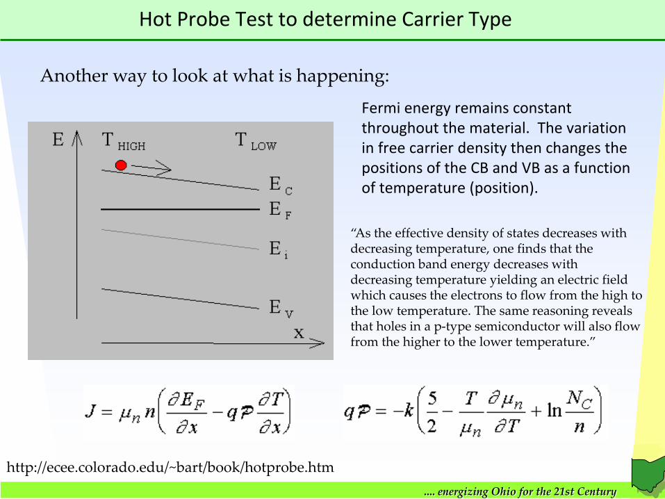
Hot Probe Test to determine Carrier Type
Another way to look at what is happening:
http://ecee.colorado.edu/~bart/book/hotprobe.htm
Fermi energy remains constant throughout the material. The variation in free carrier density then changes the positions of the CB and VB as a function of temperature (position).
“As the effective density of states decreases with decreasing temperature, one finds that the conduction band energy decreases with decreasing temperature yielding an electric field which causes the electrons to flow from the high to the low temperature. The same reasoning reveals that holes in a p-type semiconductor will also flow from the higher to the lower temperature.”

.... energizing Ohio for the 21st Century
Rectifying behavior
I–V characteristics of a P-N junction diode (not to scale). From http://en.wikipedia.org/wiki/Diode