solar explorer kit hardware and control reference guide
TRANSCRIPT
Solar Explorer Reference
Version 1.0 – January 31, 2012
1. Introduction
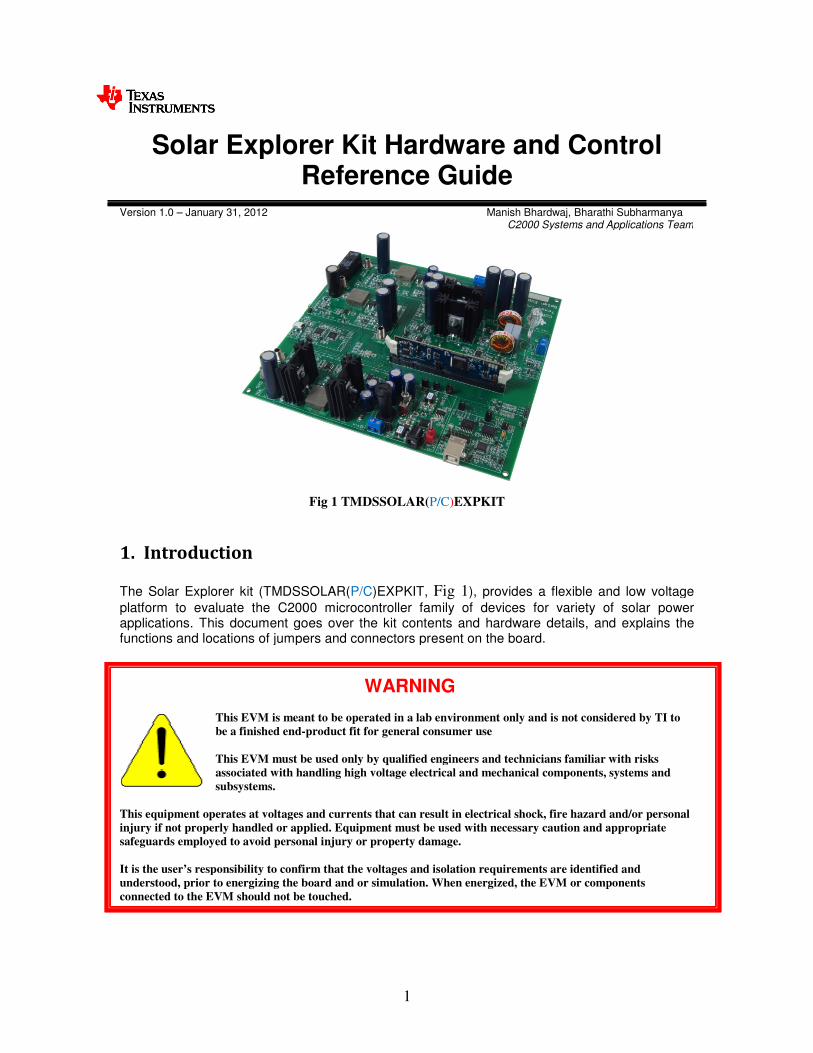
The Solar Explorer kit (TMDSSOLAR
platform to evaluate the C2000 microcontroller family of devices for applications. This document goes over functions and locations of jumpers and connectors present on the board.
This EVM is meant to be operated in a lab
be a finished end-
This EVM must be used only by
associated with handling high voltage electrical and mechanical
subsystems.
This equipment operates at voltages and currents that can result in electrical shock, fire hazard and/or
injury if not properly handled or applied.
safeguards employed to avoid personal
It is the user’s responsibility to confirm
understood, prior to energizing the board
connected to the EVM should not be touched.
1
Solar Explorer Kit Hardware and Control
Reference Guide Manish Bhardwaj, Bharathi Subharmanya
C2000 Systems and Applications Team
Fig 1 TMDSSOLAR(P/C)EXPKIT
SOLAR(P/C)EXPKIT, Fig 1), provides a flexible and low voltage
C2000 microcontroller family of devices for variety of solar power This document goes over the kit contents and hardware details, and explains the
functions and locations of jumpers and connectors present on the board.
WARNING
This EVM is meant to be operated in a lab environment only and is not considered by TI to
-product fit for general consumer use
be used only by qualified engineers and technicians familiar with risk
associated with handling high voltage electrical and mechanical components, systems and
voltages and currents that can result in electrical shock, fire hazard and/or
injury if not properly handled or applied. Equipment must be used with necessary caution and appropriate
personal injury or property damage.
’s responsibility to confirm that the voltages and isolation requirements are identified and
prior to energizing the board and or simulation. When energized, the EVM or compon
not be touched.
and Control
Manish Bhardwaj, Bharathi Subharmanya C2000 Systems and Applications Team
le and low voltage
variety of solar power and explains the
and is not considered by TI to
ngineers and technicians familiar with risks
mponents, systems and
voltages and currents that can result in electrical shock, fire hazard and/or personal
appropriate
identified and
the EVM or components

2
Contents 1. Introduction ................................................................................................................. 1
2. Getting Familiar with the Kit ...................................................................................... 3
2.1 Kit Contents.......................................................................................................... 3
2.2 Kit Overview ........................................................................................................ 3
3. Power Stages on the Kit .............................................................................................. 4
3.1 Macros Location & Nomenclature ....................................................................... 4
3.1 Boost DC-DC Single Phase with MPPT .............................................................. 6
Power Stage Parameters .............................................................................................. 6
Control Description ..................................................................................................... 6
3.2 DC-DC Battery Charging, Sepic .......................................................................... 7
Power Stage Parameters .............................................................................................. 8
Control Description ..................................................................................................... 8
3.3 Single Phase Inverter ......................................................................................... 10
Power Stage Parameters ............................................................................................ 10
Control Structure ....................................................................................................... 10
3.4 PV Emulator ....................................................................................................... 13
Power Stage Parameters ............................................................................................ 13
Control Description ................................................................................................... 14
3.5 DC Link Capacitor Requirement........................................................................ 18
4 PV Systems using Solar Explorer Kit ....................................................................... 20
4.1 PV DC-DC Systems ........................................................................................... 20
4.2 PV Grid Tied Inverter ........................................................................................ 22
4.3 PV Off Grid Inverter .......................................................................................... 24
5 Hardware Details ...................................................................................................... 26
5.1 Resource Allocation ........................................................................................... 26
5.2 Jumpers and Connectors..................................................................................... 29
5.3 GUI Connection ................................................................................................. 30

3
2. Getting Familiar with the Kit
2.1 Kit Contents
The kit follows the control card concept and hence any device from the C2000 family with DIMM100 control card can be used with the kit. The kit is available with two part numbers, TMDSSOLARPEXPKIT and TMDSSOLARCEXPKIT. The TMDSSOLARPEXPKIT ships with F28035 MCU control card, which is part of the Piccolo family in the C2000 MCU product line and highlights the control of the solar power stage. The TMDSSOLARCEXPKIT ships with the F28M35x control card, which is part of the Concerto family and has heterogeneous dual cores, where one handles the control of the power stage and the other handles the communication such as USB, Ethernet etc. highlighting control and communication using a single MCU. The kit consists of
• F28M3H52C controlCARD (TMDSSOLARCEXPKIT)
• F28035 controlCARD (TMDSSOLARPEXPKIT)
• Solar Explorer Base Board
• 20V 2 Amps Power Supply
• Banana Plug Cords (installed on the board)
• 50W 24Vac Light Bulb
• USB-B to A Cable
• USB mini to A Cable The control cards are pre-flashed to run with the respective GUI for a quick demo. All the software projects are available for the kit through controlSUITE.
2.2 Kit Overview
The Solar Panel or PhotoVoltaic (PV) panel, as it’s more commonly called, is a DC source with a non linear V vs I characteristics. The key challenges in PV system design are to extract maximum power from the panel by operating at the maximum power point (MPP) of this non linear V vs I curve of the panel, and to convert the power such that it can be used to charge batteries, run DC loads, run AC loads, or feed power into the electrical grid. A variety of power topologies are used for different PV based systems depending on system requirements. The Texas Instruments C2000 microcontroller family, with its enhanced peripheral set and optimized CPU core for control tasks, is ideal for these solar power control applications.
Fig 2 gives a block diagram of different stages present on the Solar Explorer kit to process power
from the solar panel. The input to the solar explorer kit is a 20V DC power supply which powers the controller and the supporting circuitry. A 50W solar panel can be connected to the board (Typical values Vmpp 17V, Pmax 50W). However for quick demonstration of the power processing from the solar panel, a PV emulator power stage is integrated on the board along with other stages that are needed to process power from the panel. The control of the PV panel is kept separate from the control of the other stages. Thus, the board uses two C2000 controllers, a dedicated Piccolo-A device is present on the base board and is used to control the PV emulator stage. The other stages such as, DC-DC Boost and DC-AC and DC-DC Sepic are controlled by a single C2000 device using a control –card that can

4
be placed in the DIMM100 control card slot on the EVM board. Any of C2000 device with a compatible control card can be used for this operation.
Fig 2 Solar Explorer Kit Overview
PV is a light dependent source, therefore a light sensor is integrated on the board which can be used to change behavior of the panel under different lighting conditions. The various stages on the board are rated to interface with a typical 50W solar panel (refer to the detailed hardware specification of each stage for details)
3. Power Stages on the Kit
3.1 Macros Location & Nomenclature
Fig 3, shows the location of the different power stage blocks / macros present on the board.
� TMDSSOLAREXPL Kit Main Board [Main] – Consists of controlCARD socket, light sensor,
relay, communications, instrumentation (DAC’s) and routing of signals in between the macros and to the control card.
� Boost DC-DC Single Phase with MPPT [M1] – DC-DC Macro accepts DC input, which can be from the PV panel or a battery output (depending on system configuration), and boosts it. This block has the necessary input sensing to implement MPPT.
� Inverter Single Phase [M2] – DC-AC Macro accepts a DC voltage and uses a full bridge single phase inverter to generate a sine wave. The output filter, filters high frequencies, thus generating a smooth sine wave at the output.
� Sepic DC-DC with MPPT Battery Charging [M3] – DC-DC Macro accepts DC input from the PV panel and is used to charge a battery. The sepic stage provides both buck and boost capabilities that are necessary while charging the battery.

5
� Sync Buck Boost DC-DC Panel EMU [M4] – DC-DC Macro accepts DC input from the DC Power Entry Macro (20V typical) and uses it to generate the PV panel emulator output. The module senses the output voltage and current, which makes emulation of the panel’s V vs I characteristics possible.
� Pic-A USB-mini EMU [M5] – This is a macro with the TMS320F28027 microcontroller and the JTAG emulator present to control and debug the M4 stage.
� DC-PwrEntry VinSw 12V 5V 3V3 [M6] - DC Power Entry, used to generate the 12V, 5V and 3.3V for the board from 20V DC power supply supplied with the kit. This macro also supplies power for the on-board panel emulator, M4.
� ISO USB to JTAG [M7] – JTAG connection to the main board. Nomenclature: Components are referenced with the macro number in brackets, followed by the component label designator. For example, [M3]-J1 would refer to the jumper J1 located in the macro M3. Likewise, [Main]-J1 would refer to the jumper J1 located on the main board outside of any defined macro blocks.
Fig 3 Macro Block on Solar Explorer Kit

6
To enable easy debug of individual power stages input and output of the power stages are kept as terminal blocks or banana jacks. With help of a macro approach in hardware it is possible to realize different PV systems using the solar explorer kit.
3.1 Boost DC-DC Single Phase with MPPT
iC oC
Fig 4 Boost DC-DC Single Phase with MPPT Power Stage
Power Stage Parameters
Input Voltage : 0 -30V (Panel Input)
Input Current : 0- 3.5 Amps (Panel Input)
Output Voltage : 30V DC Nominal
Output Current: 0-2 Amps
Power Rating: 50W
fsw = 100Khz
Control Description
A single phase boost stage is used to boost the voltage from the panel and track the MPP
of the panel. The input current pvI is sensed before the input capacitance iC along with
the panel voltage pvV . These two values are then used by the MPPT algorithm.
The MPPT is realized using an outer voltage loop that regulates the input voltage i.e.
panel voltage by modulating the current reference for the inner current loop of the boost
stage. Increasing the current reference of the boost, i.e. current drawn through the boost,
loads the panel and hence results in the panel output voltage drop. Therefore the sign for

7
the outer voltage compensator reference and feedback are reversed. It is noted that the
output of the boost is not regulated. However to prevent the output voltage from rising
higher than rating of the components, the voltage feedback is mapped to the internal
comparators which can do a cycle by cycle trip of the PWM in case of over voltage.
Fig 5 Boost with MPPT Control Diagram
3.2 DC-DC Battery Charging, Sepic
Fig 6 DC-DC Battery Charging Sepic Power Stage

8
Power Stage Parameters
Input Voltage : 0 -30V (Panel Input)
Input Current : 0- 3.5 Amps (Panel Input)
Output Voltage : 10V-16V DC max
Output Current: 0-3.5 Amps
Power Rating: 50W Max
fsw = 200Khz
Control Description
This stage is responsible for charging a typical 12V battery from the solar panel, and
therefore has panel current pvI and panel voltage pvV sensing to track MPP of the panel.
A sepic stage was chosen to realize this function, as both buck and boost are possible
using the sepic stage. A typical lead acid battery charging can be divided into four stages,
stage determination and transition is done as:
1. Trickle Charging State: When the battery voltage is below a discharge threshold
chgenbV , the battery has been deeply discharged or has shorted cells. In this case the
charging begins with a very low trickle current tcI . If the battery cells are shorted
then the battery voltage would remain below the chgenbV , thus preventing the
charging state from going to the bulk charging stage. Otherwise the battery
voltage would slowly build up and would come within a nominal range i.e. above
chgenbV . At this stage the state would move to Bulk charging. While in Trickle
charging mode MPPT may not be needed.
2. Bulk Charging State: In this stage the charger acts like a current source for the
battery providing a constant current bulkI . As the PV may not be able to supply the
ideal bulkI to charge the battery, however it tries its best by operating at MPP. As
the battery voltage exceeds 0.95 ocV , the charger enters the Over Charger Mode.
3. Over Charging State: The role of this state is to restore the full capacity in
minimum amount of time at the same time avoiding over charging. All the battery
voltage and current loop are enabled while MPPT is disabled. fBattV Re now equals
ocV . Initially overcharge current equals bulk charge current, but as over charge
voltage is approached, the charge current diminishes. IBref is determined by the
voltage loop.
4. Float Charge State: During this state the battery voltage is maintained at floatV to
maintain battery capacity against self discharge. The charger would deliver as
much current is needed for sustaining the float voltage.

9
The battery would remain in the float state until the battery voltage drops below 90%
of the float voltage due to discharging at which point operation is reverted to bulk
charging.
Typical values for 12V battery are
Overcharge Voltage, ocV =15V
Floating Voltage, floatV = 13.5V
Discharge Threshold, chgenbV = 10.5V
Load disconnect voltage, ldvV = 11.4
Load reconnect voltage, rvV = 12.6V
The following block diagram illustrates the control proposed for this stage when doing
MPPT. The control when doing MPPT is similar to the boost stage however when the
battery is not in the bulk charging stage the MPP cannot be maintained as the battery
cannot absorb the max power from the panel.
Hence the control of the stage changes from input voltage of the stage/ output of the
panel regulation to the output voltage of the stage regulation. The instance when the
control is switched is dependent on the battery type and charging algorithm.
Fig 7 Battery Charging with MPPT Control Diagram

10
3.3 Single Phase Inverter
Signal I/F Conditioning
Drivers
Fig 8 Single Phase Full Bridge Inverter Power Stage
Power Stage Parameters
Input Voltage : 30V DC Nominal
Input Current : 0- 2 Amps
Output Voltage : 20-24Vrms Max
Output Current: 0-2 Amps
Power Rating: 50W
fsw = 10Khz-20Khz
Control Structure
To appreciate the control of a full bridge inverter, first the mechanism how the High
Frequency Full Bridge Inverter feeds current into the grid/line needs to be understood.
Several modulation schemes exist for achieving this, the following derivations uses the
Unipolar Modulation to scheme to analyze the current fed form the converter.
Current Control

11
In a unipolar modulation scheme, alternate legs are switched depending on which half of
the sine of the AC signal is being generated.
Positive Half: SW1 and SW2 are modulated & SW4 is always ON, SW3 is always OFF
Negative Half: SW3 and SW4 are modulated & SW2 is always ON, SW1 is always OFF
This modulation scheme is highlighted in the following figure.
LCL filter at the output of the inverter filters this waveform. Now the voltage across the
LCL filter can be written as
griddconLCL vVV −=, , when SW1 and SW4 are conducting,
griddconLCL vVV −−=, , when SW3 and SW4 are conducting,

12
gridoffLCL vV −=, , when SW2 and SW4 are conducting,
Thus the change in grid current per switching cycle is computed as:
)(
*
)(
)1)(0(
)(
).(
swLCL
griddc
swLCL
grid
swLCL
griddc
gridFZ
vDV
FZ
Dv
FZ
DvVi
−=
−−+
−=∆
From this equation it is noted that the current can be controlled by varying the Duty
Cycle. Typically a current transformer is used to measure the gird current. However on
the Explorer kit as this is a learning platform shunt current measurement is used.
Two shunt current measurement resistors are placed, the grid current (i.e. the current fed
into the grid from the inverter) is estimated by subtracting the two leg currents).
12 legleggrid iii −=∆
Let’s assume positive half of the sine wave i.e. we should feed current into the grid
Vdc
Q2
C1
Cac
Q1
Q4
Ileg2Ileg1
Q3
Grid
L1
L2
Vline
Vneutral
Primary Current fed into the grid during the positive half is 2legi , 1legi will measure zero.
However when the current reference for the inverter is very low i.e. Q1 is open most of
the times, this can result in shorting the grid across SW2 and SW4. When shorted a high
current flows through both Leg1 and Leg2. This is why the Leg1 current is subtracted
from the Leg1 current at all times to get the change in the grid current.
13
Vdc
Q2
C1
Cac
Q1
Q4
Ileg2Ileg1
Q3
Grid
L1
L2
Vline
Vneutral
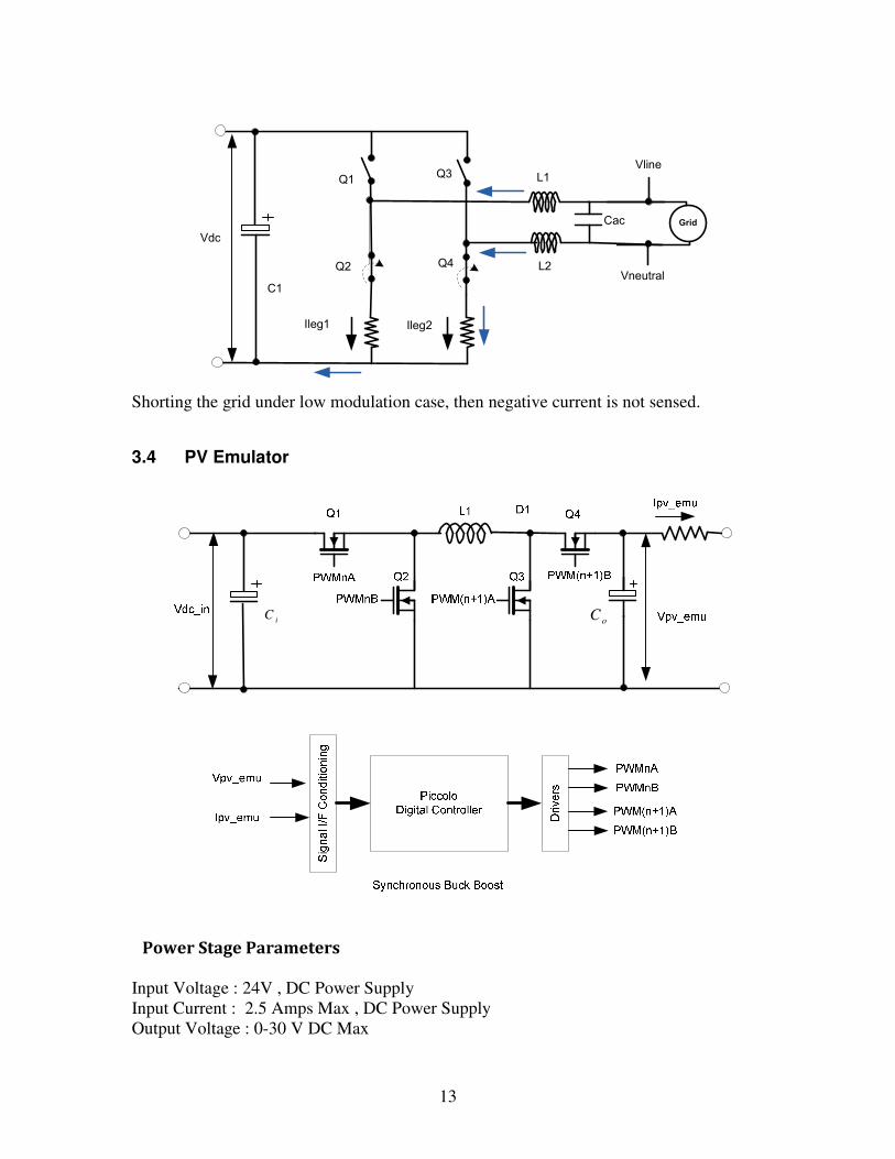
Shorting the grid under low modulation case, then negative current is not sensed.
3.4 PV Emulator
iCoC
Power Stage Parameters
Input Voltage : 24V , DC Power Supply
Input Current : 2.5 Amps Max , DC Power Supply
Output Voltage : 0-30 V DC Max
14
Output Current: 0-2.5 Amps
Power Rating: 50W Max
fsw = 200Khz
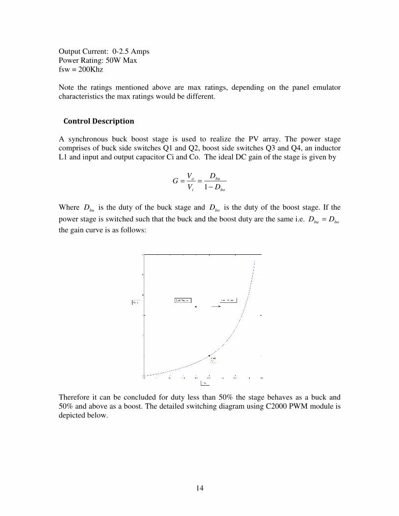
Note the ratings mentioned above are max ratings, depending on the panel emulator
characteristics the max ratings would be different.
Control Description
A synchronous buck boost stage is used to realize the PV array. The power stage
comprises of buck side switches Q1 and Q2, boost side switches Q3 and Q4, an inductor
L1 and input and output capacitor Ci and Co. The ideal DC gain of the stage is given by
bo
bu
i
o
D
D
V
VG
−==
1
Where buD is the duty of the buck stage and boD is the duty of the boost stage. If the
power stage is switched such that the buck and the boost duty are the same i.e. bobu DD =
the gain curve is as follows:
Therefore it can be concluded for duty less than 50% the stage behaves as a buck and
50% and above as a boost. The detailed switching diagram using C2000 PWM module is
depicted below.

15
This stage is controlled using Piccolo-A (F28027) which is present on the EVM base
board. This controller is separate from the controller that does the DC-DC boost, battery
charging and the DC-AC conversion present on the board.
The input voltage to the buck boost stage is from the DC Power entry block. This voltage
is 20V, as the power adapter shipped with the kit is 20V. However the user can use
another voltage input by connecting it to the Terminal Block present on the board.
To emulate the panel characteristics the stage needs to operate as a current controlled
voltage source i.e. depending on the load current demand the output voltage will change.
This is achieved by changing the voltage reference of the stage based on look up table
value.
The current being drawn by the panel pvI is used as the index for the look up table that is
stored on the controller. The look up table is then used to provide the voltage reference
refpvV _ for the panel corresponding to the pvI . A light sensor is placed on the board to
control the irradiance level and produce a corresponding V-I curve. For getting curves

16
between different luminance levels the values from the stored curve are interpolated
using the following equation.
refpvGrefpv VG
GV _2__ *
1
2=
Where G2 is the new luminance value and G1 is the old luminance value. (Note this is
just an approximation of the PV characteristics, the real panel characteristics may differ)
Following are the curves of the PV emulator table that is stored for the PV emulation on
the controller.

17
Luminance Ratio
(w.r.t 1000W/m^2)
Pmpp
=(Pmax * Luminance Ratio)
Watts
Vmpp
(Volts)
1.0 = 1000 W/m^2 36.02 18.46
0.9 = 900W/m^2 32.42 16.42
0.8 = 800W/m^2 28.82 14.68
0.7 = 700W/m^2 25.22 12.77
0.6= 600W/m^2 21.61 10.98
0.5=500W/^2 18.01 9.093
0.4=400W/m^2 14.41 7.363
0.3=300W/m^2 10.81 5.473
0.2=200W/m^2 7.205 3.67
Note in a PV inverter system the DC-DC Boost stage feeds the input to the inverter stage.
As the inverter provides an AC load which causes a 100-120Hz ripple (depending on the
frequency of the AC load) on the DC bus of the inverter. A DC Link capacitor is typically
used to compensate for this power ripple.

18
3.5 DC Link Capacitor Requirement
Note in a PV inverter system the DC-DC Boost stage feeds the input to the inverter stage.
As the inverter provides an AC load which causes a 100-120Hz ripple (depending on the
frequency of the AC load) on the DC bus of the inverter. A DC Link capacitor is typically
used to compensate for this power ripple. The following derivation shows the relation
between this DC Link capacitor and ripple on the DC Bus.
)sin( wtii pkac =
)sin( wtvv pkac =
))2cos(1(2
1. wtviivp pkpkacacac −==
dcdcdc IVp .=
acv
aci
acp
dcP
dcV
Let the AC current being fed to the grid/ load and the AC voltage be:
)sin(
)sin(
wtVv
wtIi
pkac
pkac
=
=
Which implies the power supplied by the inverter is:
)]2cos(1[2
1* wtIVivp pkpkacacac −==

19
In the equation the power injected into a single-phase grid follows a sinusoidal waveform
with twice the frequency of the grid. The PV module cannot be operated at the MPP if
this alternating power is not decoupled by means of an energy buffer. Therefore a
capacitor bank is typically used for buffering this energy.
To estimate the amount of capacitance needed to buffer this energy, let the magnitude of
the ripple induced on the DC bus due to the alternating nature of the power being drawn
be V∆ . Now Looking at a quarter of the sinusoidal power waveform the equation for the
power being drawn for 1/8th
of the grid cycle can be written as follows:
))((***4
)*8(
1
)(2
1
2
1
8
22
22
VVVCf
f
VVCCV
T
EP ac
ac
ac ∆−−=
∆−−
=∆
=
Now assuming the inverter can deal with a 10% voltage ripple on the input DC bus we
get the Capacitance required for this stage.
))((**422
VVVf
PC
ac
ac
∆−−=
As is clear from the equation the minimum capacitance required is a function of the value
of voltage this energy buffer is kept at and the AC power delivered.
20
4 PV Systems using Solar Explorer Kit
PV energy can be utilized in a wide variety of fashion, from powering street light,
feeding current into the grid, powering remote base stations etc. The solar explorer kit
can be used to experiment with a variety of these applications.
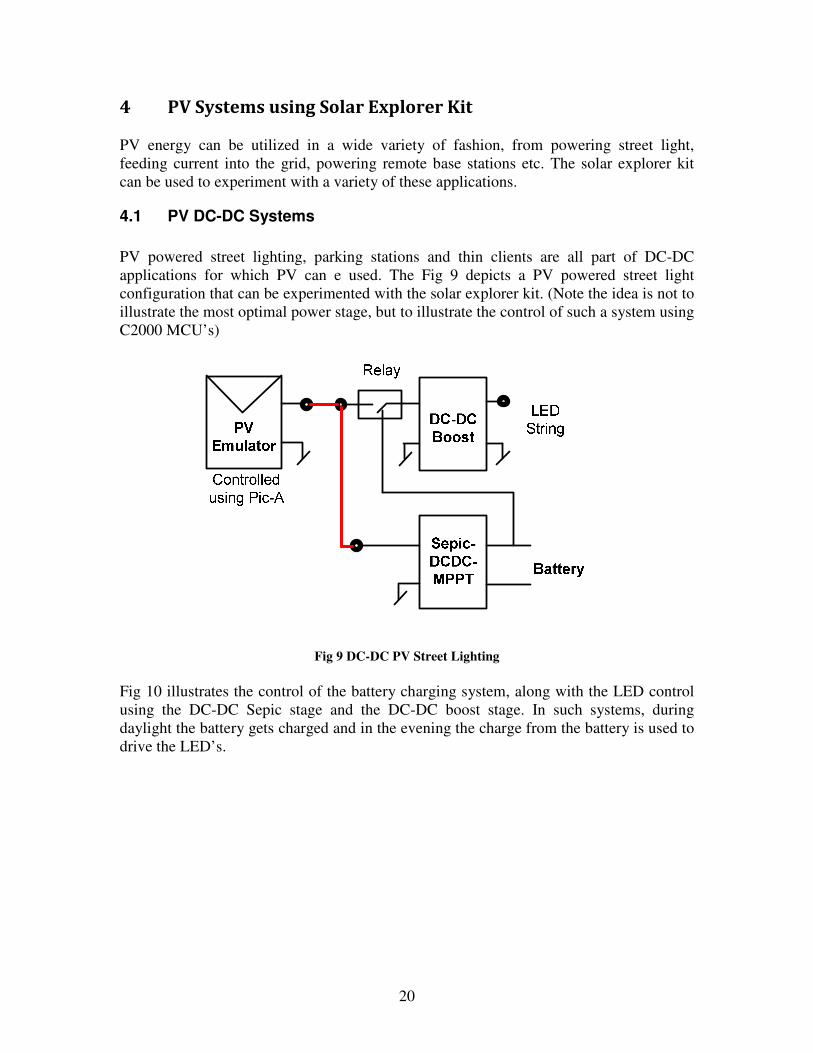
4.1 PV DC-DC Systems
PV powered street lighting, parking stations and thin clients are all part of DC-DC
applications for which PV can e used. The Fig 9 depicts a PV powered street light
configuration that can be experimented with the solar explorer kit. (Note the idea is not to
illustrate the most optimal power stage, but to illustrate the control of such a system using
C2000 MCU’s)
Fig 9 DC-DC PV Street Lighting
Fig 10 illustrates the control of the battery charging system, along with the LED control
using the DC-DC Sepic stage and the DC-DC boost stage. In such systems, during
daylight the battery gets charged and in the evening the charge from the battery is used to
drive the LED’s.
21
Fig 10 Control of PV Street Light with Battery Charging

22
4.2 PV Grid Tied Inverter
PV energy can be fed into the grid using a current control inverter. A typical PV Grid tied
inverter uses a boost stage to boost the voltage from the PV panel such that the inverter
can feed current into the grid. (The DC Bus of the inverter needs to be higher than the
maximum Grid Voltage) Fig 11 illustrates a typical grid tied PV inverter using the
macros present on the solar explorer kit.
Fig 11 PV Grid Tied Inverter
The DC-DC stage is responsible to maintain MPPT of the panel and the inverter is
responsible for the synchronization with the grid and feeding current into the grid. Fig 12
shows the control of a PV inverter stage.

23
Fig 12 Control of PV Grid Tied Inverter
24
4.3 PV Off Grid Inverter
PV energy is not a steady source of energy, in daytime the PV generates power whereas
at night time it does not generate any power. For PV to supply power to a standalone
installation a power storage element is needed, this is done with help of a battery
charging stage. Such a system can be realized using the solar explorer kit as shown in the
Fig 13. The controls of such a system are described in the Fig 14.
Fig 13 PV Off Grid Inverter System

25
Fig 14 PV Off Grid Inverter Control

26
5 Hardware Details
5.1 Resource Allocation
The Fig 15 shows the various stages of the board in a block diagram format and illustrates the
major connections and feedback values that are being mapped to the C2000 MCU. Table 1,
below lists these resources. The table below only lists the resources used for power stages that convert power from the panel and that are mapped to the DIMM100 connector on the board, and not of the panel emulation stage.
Table 1 Resource Mapping: PWM, ADC, GPIO, Comms
Macro Name Signal Name
PWM Channel/
ADC Channel No/ Resource Mapping
F2803x
PWM Channel/
ADC Channel No/ Resource Mapping
F28M35x
Function
Single Phase Inverter
PWM-1L PWM-1A PWM-1A Inverter drive PWM
PWM-1H PWM-1B PWM-1B Inverter drive PWM
PWM-2L PWM-2A PWM-2A Inverter drive PWM
PWM-2H PWM-2B PWM-2B Inverter drive PWM
Ileg1-fb ADC-A4 ADC1-A4 Leg1 Current
Ileg2-fb ADC-A6 ADC1-A6 Leg2 Current
VL-fb ADC-B1 ADC2-B0 Line Voltage Feedback
VN-fb ADC-A5 ADC1-B4 Neutral Voltage Feedback
Vac-fb ADC-A7 ADC1-A7 AC Voltage Feedback
VdcBus-fb ADC-A3 ADC1-A3 DC Bus Voltage Feedback
ZCD ECAP1 ECAP1 ZCD Capture
DC-DC Single Phase Boost with MPPT
PWM PWM-3A PWM-3A Boost PWM
Vpv-fb ADC-A1 ADC1-B0 Panel Voltage Feedback
Ipv-fb ADC-A0 ADC1-A0 Panel Current Feedback
Iboostsw-fb ADC-B6 ADC2-A6 Boost Switched Current
Vboost-fb ADC-A2 ADC1-A2 Boost Voltage Feedback
DC-DC Sepic with MPPT
PWM PWM-4A PWM-4A Sepic PWM
Vpnl-fb ADC-B2 ADC2-A2 Panel Voltage Feedback
Ipnl-fb ADC-B3 ADC2-A3 Panel Current Feedback
Ibattsw-fb ADC-B7 ADC2-A7 Battery Switched Current
Vbatt-fb ADC-B4 ADC2-A4 Battery Voltage
Main –Board RLY-en GPIO-12 GPIO-12 Relay Switch
Light-fb ADC-B0 ADC2-A0 Light Sensor Feedback
PWM PWM-5A PWM-5A DAC-1
PWM PWM-6A PWM-6A DAC-2
PWM PWM-7A Not Available DAC-3
PWM PWM-7B Not Available DAC-4
SPISOMI-B SPISOMI-B SSI Comm. to PV Emu
SPISIMO-B SPISIMO-B SSI Comm. to PV Emu
SPISTE-B SPISTE-B SSI Comm. to PV Emu
SPICLK-B SPICLK-B SSI Comm. to PV Emu
Tx-slave SCITX-A Not used Comm. to SCI GUI
Rx-slave SCIRX-A Not used Comm. to SCI GUI

27
Fig 15 Solar Explorer Kit Block Diagram with C2000 MCU
(Connectivity Peripherals may differ from one device to the other inlcuding Ethernet, USB, CAN, SPI etc)

28
Fig 16 Solar Explorer Jumpers & Connectors
[M7] JP1 - USB Connection for
onboard emulation
[M7] J5 – On-board emulation disable
jumper
[M7] J2 – External JTAG emulator
interface
[Main] BS7 Banana
Connector jack for Panel Input
(750W Max Input)
[M6] J1 – Source power from DC Jack Jumper
[Main] BS3 Banana
Connector jack for Panel Input
[Main] BS2 Banana
Connector Jack for GND
Connection
[Main] J5 – DAC outputs
[Main] J4 – FTDI UART Jumper
[M7] J1 & J2– Boot Option Jumper
[M5] J1 – PV Emulator Reset
jumper
[M6] SW2 – 12, 5 , 3.3VDC
power switch
[Main] BS5 – Banana Connector
Jack for GND Connection
[Main] J1-J3 – jumper to enable
controller power (12, 5 and 3.3VDC) from the 20V DC power
supply
[M7] J4– JTAG TRSTn Jumper
JupjumperOption
[M6] JP1 – DC Jack for 20V DC
power supply
[Main] BS4 Banana
Connector jack for Boost Output
Voltage
[Main] BS1 Banana
Connector for Panel Emulator
Output
[Main] TB2 – Terminal Connector
for Battery Pack Connection
[Main] U1 Light Sensor
[Main] BS5 – Banana Connector
Jack for Inverter Input
[M6] TB1 – External Power Supply Connection
terminal Block
[M5] JP1 – miniUSB
Connection for emulation of PV
Panel
[M6] SW1 – Panel Emulator Power
Rail On/Off
[Main] TB1 – Inverter Output

29
5.2 Jumpers and Connectors
Table 2 below shows the various connections available on the board, and is split up by the
macro each connection is included in. Fig 16 above, illustrates the location of these connections
on the board with help of a board image:
Table 2 Jumpers & Connectors on Solar Explorer Board
[Main]-BS1 Banana Jack for Panel Emulator Output Connection [Main]-BS2, BS6 Banana Jack for GND Connection [Main]-BS3, BS7 Banana Jack for Panel Input Connection [Main]-BS4 Banana Jack for Boost Voltage Connection [Main]-BS5 Banana Jack for connecting the input to the DC-AC inverter, typically
this is the Boost Output an input voltage [Main] J1, J2, J3 Jumpers J1,J2 and J3 are used for sourcing 12V, 5V and 3.3V power
respectively for the board from the DC Power Entry block [M6] on the board
[Main] J4 JTAG TRSTn disconnect jumper, populating the jumper enables JTAG connection to the microcontroller. The jumpers needs to be unpopulated when no JTAG connection is required such as when booting from FLASH
[Main] J5 DAC outputs: Gives voltage outputs that result from a PWM being attached to a first-order low-pass filter. Pins 1,2,3 and 4 are attached to low pass filtered PWM-5A, PWM-6A, PWM-7A and PWM-7B respectively. These are used in conjunction with the PWMDAC DMC library components to observe system variables on an oscilloscope
[Main]-H1 DIMM100 Connector, used to insert the C2000 MCU control card [Main]-TB2 Terminal Block for output of Sepic stage[M3], used to connect to
battery pack [M2]-TB1 Inverter Output Voltage Connection Terminal Block [M6]-JP1 DC Power Jack, Input Connection from the DC Power Supply [M6]-SW1 Switch to enable/disable power to the PV Emulator stage, When in
ON position 20V from the DC Power entry macro goes to the Panel Emulator stage
[M6]-SW2 Switch to enable/disable power to the board. When in On position the input voltage is used to generate 12V, 3.3V and 5V rail on the board. Also if the [M6]-J1 jumper is populated the power from the DC Jack is also used for the power rail of the Panel Emulator Stage
[M6]-J1 When jumper is populated the power for the PV emulator stage is the input of the DC Power Jack [M6]-JP1. When unpopulated a separate external power supply can be connected to [M6]-TB1 to source power for the Panel Emulator Stage.
[M6]-TB1 External Power supply connection for the PV emulator, the PV emulator can source power from the 20V power supply that feeds into [M6]-JP1, however if it is desired an external power supply can be connected to [M6]-TB1 which will separate the DC Link from the controller power. When using external power supply [M6]-J1 needs to be depopulated.
[M7]-JP1 USB connection for on-board emulation [M7]-J1&J3 Boot Option Jumpers, not used for F2802x, F2803x or F2833x
devices. [M7]-J2 External JTAG interface: this connector gives access to the JTAG
emulation pins. If external emulation is desired, place a jumper across [M3] J5 and connect the emulator to the board. To power the

30
emulation logic a USB connector will still need to be connected to [M7] JP1.
[M7]-J4 Populate when using FTDI chip as a UART i.e. when using a GUI to interact with the MCU.
[M7]-J5 On-board emulation disable jumper: Place a jumper here to disable the on-board emulator and give access to the external interface.
5.3 GUI Connection
The FTDI chip present on the board can be used as an isolated SCI for communicating with a HOST i.e. PC. The following jumper settings must be done to enable this connection. As the GUI software with SCI is provided for F28035 control card only, F28035 settings are discussed below, 1. Populate the jumper [M7]-J4 2. Remove the jumper [Main]-J4, this disables JTAG connection. 3. For F28035, put SW3 on the F28035 Control Card to OFF position 4. Connect a USB cable from [M7]-JP1 to host PC.
Note: If you are going to boot from Flash & connecting using the GUI, you would need to do the Boot from Flash settings as described in the Table Boot Options.

31
SCHEMATIC DISCLAIMER AND WARNINGS
TI provides the High Voltage DMC and PFC kit schematic drawings to help users
develop C2000 based reference design products. Application safety, safety of the
High Voltage DMC and PFC kit and design integrity of such reference designs are
solely responsibility of the user. Any reference designs generated off these
schematics must take into account necessary product safety design requirements,
including interface components and load motors in order to avoid user risks including
potential for fire hazard, electrical shock hazard and personal injury, including
considerations for anticipated agency certification compliance requirements.
Such product safety design criteria shall include but not be limited to critical circuit
creepages and clearances, component selection, ratings compatibility of controlled
motor loads, and required protective means (ie output fusing) depending on the
specific loads being controlled.
TI accepts no responsibility for design integrity of any reference designs based on
supplied schematic drawings and the schematics are strictly for development
purposes.
EVALUATION BOARD/KIT IMPORTANT NOTICE
Texas Instruments (TI) provides the enclosed product(s) under the following
conditions:
This evaluation board/kit is intended for use for ENGINEERING DEVELOPMENT,
DEMONSTRATION, OR EVALUATION PURPOSES ONLY and is not considered by
TI to be a finished end-product fit for general consumer use. Persons handling the
product(s) must have electronics training and observe good engineering practice
standards. As such, the goods being provided are not intended to be complete in
terms of required design-, marketing-, and/or manufacturing-related protective
considerations, including product safety and environmental measures typically found
in end products that incorporate such semiconductor components or circuit boards.
This evaluation board/kit does not fall within the scope of the European Union
directives regarding electromagnetic compatibility, restricted substances (RoHS),
recycling (WEEE), FCC, CE or UL, and therefore may not meet the technical
requirements of these directives or other related directives.
Should this evaluation board/kit not meet the specifications indicated in the User’s
Guide, the board/kit may be returned within 30 days from the date of delivery for a
full refund. THE FOREGOING WARRANTY IS THE EXCLUSIVE WARRANTY MADE BY
SELLER TO BUYER AND IS IN LIEU OF ALL OTHER WARRANTIES, EXPRESSED,
IMPLIED, OR STATUTORY, INCLUDING ANY WARRANTY OF MERCHANTABILITY OR
FITNESS FOR ANY PARTICULAR PURPOSE.
The user assumes all responsibility and liability for proper and safe handling of the
goods. Further, the user indemnifies TI from all claims arising from the handling or
use of the goods. Due to the open construction of the product, it is the user’s
responsibility to take any and all appropriate precautions with regard to electrostatic
discharge.
EXCEPT TO THE EXTENT OF THE INDEMNITY SET FORTH ABOVE, NEITHER PARTY
SHALL BE LIABLE TO THE OTHER FOR ANY INDIRECT, SPECIAL, INCIDENTAL, OR
CONSEQUENTIAL DAMAGES.
TI currently deals with a variety of customers for products, and therefore our
arrangement with the user is not exclusive.

32
TI assumes no liability for applications assistance, customer product design,
software performance, or infringement of patents or services described
herein.
Please read the User’s Guide and, specifically, the Warnings and Restrictions notice
in the User’s Guide prior to handling the product. This notice contains important
safety information about temperatures and voltages. For additional information on
TI’s environmental and/or safety programs, please contact the TI application
engineer or visit www.ti.com/esh.
No license is granted under any patent right or other intellectual property right of TI
covering or relating to any machine, process, or combination in which such TI
products or services might be or are used.
Mailing Address:
Texas Instruments
Post Office Box 655303
Dallas, Texas 75265
Copyright © 2010, Texas Instruments Incorporated
FCC Warning
This evaluation board/kit is intended for use for ENGINEERING DEVELOPMENT,
DEMONSTRATION, OR EVALUATION PURPOSES ONLY and is not considered by
TI to be a finished end-product fit for general consumer use. It generates, uses, and
can radiate radio frequency energy and has not been tested for compliance with the
limits of computing devices pursuant to part 15 of FCC rules, which are designed to
provide reasonable protection against radio frequency interference. Operation of this
equipment in other environments may cause interference with radio
communications, in which case the user at his own expense will be required to take
whatever measures may be required to correct this interference.